u blox 2AGQN4NNN Cellular Module User Manual SARA R4 series
u-blox AG Cellular Module SARA R4 series
UserManual.wiki
>
u blox
>
2AGQN4NNN User Manual
>
User Manual 2
Contents
1.
User Manual
2.
Users Manual
3.
User Manual 1
4.
User Manual 2
5.
AdhereTech User Manual
User Manual 2
Navigation menu
Upload a User Manual
Namespaces
Wiki Guide
HTML
PDF
Info
Views
User Manual
Discussion / Help
Navigation
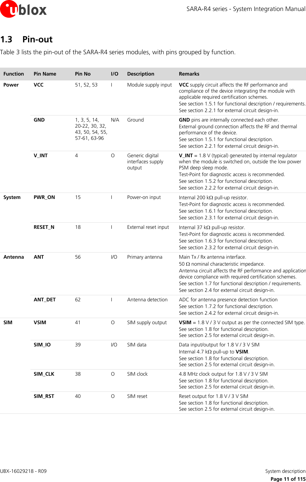
![SARA-R4 series - System Integration Manual UBX-16029218 - R09 System description Page 12 of 115 Function Pin Name Pin No I/O Description Remarks UART RXD 13 O UART data output 1.8 V output, Circuit 104 (RXD) in ITU-T V.24, for AT commands, data communication, FOAT. See section 1.9.1 for functional description. See section 2.6.1 for external circuit design-in. TXD 12 I UART data input 1.8 V input, Circuit 103 (TXD) in ITU-T V.24, for AT commands, data communication, FOAT. Internal active pull-down to GND on “00”, “02” versions Internal active pull-up to V_INT on “01” versions See section 1.9.1 for functional description. See section 2.6.1 for external circuit design-in. CTS 11 O UART clear to send output 1.8 V output, Circuit 106 (CTS) in ITU-T V.24. Not supported by ‘00’, ‘01’ and R410M-02B product versions See section 1.9.1 for functional description. See section 2.6.1 for external circuit design-in. RTS 10 I UART ready to send input 1.8 V input, Circuit 105 (RTS) in ITU-T V.24. Internal active pull-up to V_INT. Not supported by ‘00’, ‘01’ and R410M-02B product versions See section 1.9.1 for functional description. See section 2.6.1 for external circuit design-in. DSR 6 O UART data set ready output 1.8 V, Circuit 107 in ITU-T V.24. See section 1.9.1 for functional description. See section 2.6.1 for external circuit design-in. RI 7 O UART ring indicator output 1.8 V, Circuit 125 in ITU-T V.24. See section 1.9.1 for functional description. See section 2.6.1 for external circuit design-in. DTR 9 I UART data terminal ready input 1.8 V, Circuit 108/2 in ITU-T V.24. Internal active pull-up to V_INT. See section 1.9.1 for functional description. See section 2.6.1 for external circuit design-in. DCD 8 O UART data carrier detect output 1.8 V, Circuit 109 in ITU-T V.24. See section 1.9.1 for functional description. See section 2.6.1 for external circuit design-in. USB VUSB_DET 17 I USB detect input VBUS (5 V typical) USB supply generated by the host must be connected to this input pin to enable the USB interface. Test-Point for diagnostic / FW update strongly recommended. See section 1.9.2 for functional description. See section 2.6.2 for external circuit design-in. USB_D- 28 I/O USB Data Line D- USB interface for AT commands, data communication, FOAT, FW update by u-blox dedicated tool and diagnostics. 90 nominal differential impedance (Z0) 30 nominal common mode impedance (ZCM) Pull-up or pull-down resistors and external series resistors as required by the USB 2.0 specifications [4] are part of the USB pin driver and need not be provided externally. Test-Point for diagnostic / FW update strongly recommended. See section 1.9.2 for functional description. See section 2.6.2 for external circuit design-in. USB_D+ 29 I/O USB Data Line D+ USB interface for AT commands, data communication, FOAT, FW update by u-blox dedicated tool and diagnostics. 90 nominal differential impedance (Z0) 30 nominal common mode impedance (ZCM) Pull-up or pull-down resistors and external series resistors as required by the USB 2.0 specifications [4] are part of the USB pin driver and need not be provided externally. Test-Point for diagnostic / FW update strongly recommended. See section 1.9.2 for functional description. See section 2.6.2 for external circuit design-in.](https://usermanual.wiki/u-blox/2AGQN4NNN.User-Manual-2/User-Guide-3940431-Page-12.png)
![SARA-R4 series - System Integration Manual UBX-16029218 - R09 System description Page 13 of 115 Function Pin Name Pin No I/O Description Remarks SPI I2S_WA / SPI_MOSI 34 O SPI MOSI SPI Master Output Slave Input, alternatively configurable as I2S word alignment Not supported by “00”, “01” and “02” product versions. See section 1.9.3 for functional description. See section 2.6.3 for external circuit design-in. I2S_RXD / SPI_MISO 37 I SPI MISO SPI Master Input Slave Output, alternatively configurable as I2S receive data Not supported by “00”, “01” and “02” product versions. See section 1.9.3 for functional description. See section 2.6.3 for external circuit design-in. I2S_CLK / SPI_CLK 36 O SPI clock SPI clock, alternatively configurable as I2S clock Not supported by “00”, “01” and “02” product versions. See section 1.9.3 for functional description. See section 2.6.3 for external circuit design-in. I2S_TXD / SPI_CS 35 O SPI Chip Select SPI Chip Select, alternatively configurable as I2S transmit data Not supported by “00”, “01” and “02” product versions. See section 1.9.3 for functional description. See section 2.6.3 for external circuit design-in. SDIO SDIO_D0 47 I/O SDIO serial data [0] Not supported by “00”, “01” and “02” product versions. See section 1.9.4 for functional description. See section 2.6.4 for external circuit design-in. SDIO_D1 49 I/O SDIO serial data [1] Not supported by “00”, “01” and “02” product versions. See section 1.9.4 for functional description. See section 2.6.4 for external circuit design-in. SDIO_D2 44 I/O SDIO serial data [2] Not supported by “00”, “01” and “02” product versions. See section 1.9.4 for functional description. See section 2.6.4 for external circuit design-in. SDIO_D3 48 I/O SDIO serial data [3] Not supported by “00”, “01” and “02” product versions. See section 1.9.4 for functional description. See section 2.6.4 for external circuit design-in. SDIO_CLK 45 O SDIO serial clock Not supported by “00”, “01” and “02” product versions. See section 1.9.4 for functional description. See section 2.6.4 for external circuit design-in. SDIO_CMD 46 I/O SDIO command Not supported by “00”, “01” and “02” product versions. See section 1.9.4 for functional description. See section 2.6.4 for external circuit design-in. DDC SCL 27 O I2C bus clock line 1.8 V open drain, for communication with I2C-slave devices. Internal pull-up to V_INT: external pull-up is not required. Not supported by “00” and “01” product versions. See section 1.9.5 for functional description. See section 2.6.5 for external circuit design-in. SDA 26 I/O I2C bus data line 1.8 V open drain, for communication with I2C-slave devices. Internal pull-up to V_INT: external pull-up is not required. Not supported by “00” and “01” product versions. See section 1.9.5 for functional description. See section 2.6.5 for external circuit design-in.](https://usermanual.wiki/u-blox/2AGQN4NNN.User-Manual-2/User-Guide-3940431-Page-13.png)
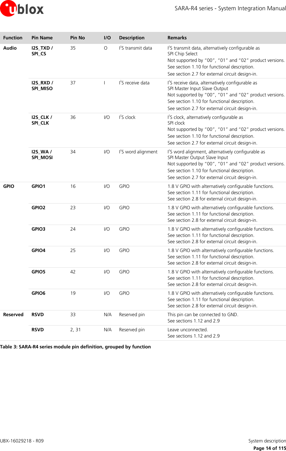
![SARA-R4 series - System Integration Manual UBX-16029218 - R09 System description Page 15 of 115 1.4 Operating modes SARA-R4 series modules have several operating modes. The operating modes are defined in Table 4 and described in detail in Table 5, providing general guidelines for operation. General Status Operating Mode Definition Power-down Not-Powered Mode VCC supply not present or below operating range: module is switched off. Power-Off Mode VCC supply within operating range and module is switched off. Normal Operation Deep-Sleep Mode RTC runs with 32 kHz reference internally generated. Active Mode Module processor core runs with 19.2 MHz reference generated by the internal oscillator Connected Mode RF Tx/Rx data connection enabled and processor core runs with 19.2 MHz reference. Table 4: SARA-R4 series modules operating modes definition Mode Description Transition between operating modes Not-Powered Module is switched off. Application interfaces are not accessible. When VCC supply is removed, the modules enter not-powered mode. When in not-powered mode, the module can enter power-off mode applying VCC supply (see 1.6.1). Power-Off Module is switched off: normal shutdown by an appropriate power-off event (see 1.6.2). Application interfaces are not accessible. The modules enter power-off mode from active mode when the host processor implements a clean switch-off procedure, by sending the AT+CPWROFF command or by using the PWR_ON pin (see 1.6.2). When in power-off mode, the modules can be switched on by the host processor using the PWR_ON input pin (see 1.6.1). When in power-off mode, the modules enter not-powered mode by removing VCC supply. Deep-Sleep Only the internal 32 kHz reference is active. The RF section and the application interfaces are temporarily disabled and switched off: the module is temporarily not ready to communicate with an external device by means of the application interfaces as configured to reduce the current consumption. The module enters the low power deep sleep mode (entering the Power Saving Mode defined in 3GPP Rel.13) whenever possible, if power saving configuration is enabled by AT+CPSMS command (see the SARA-R4 series AT Commands Manual [2]), reducing current consumption (see 1.13.9). Power saving configuration is not enabled by default; it can be enabled by AT+CPSMS (see the SARA-R4 series AT Commands Manual [2]). The modules automatically switch from the active mode to low power deep sleep mode whenever possible, upon expiration of the 6 seconds AT inactivity timer, and upon expiration of “Active Timer”, entering in the Power Saving Mode defined in 3GPP Rel.13, if power saving configuration is enabled (see 1.13.9 and the SARA-R4 series AT Commands Manual [2], AT+CPSMS command). When in low power deep sleep mode, the module switches on to the active mode upon expiration of “Periodic Update Timer” according to the Power Saving Mode defined in 3GPP Rel.13 (see 1.13.9 and the SARA-R4 series AT Commands Manual [2], AT+CPSMS command), or it can be switched on to the active mode by the host processor using the PWR_ON input pin (see section 1.6.1). Active Module is switched on with application interfaces enabled or not suspended: the module is ready to communicate with an external device by means of the application interfaces unless power saving configuration is enabled by AT+CPSMS (see the SARA-R4 series AT Commands Manual [2]). The modules enter active mode from power-off mode when the host processor implements a clean switch-on procedure by using the PWR_ON pin (see 1.6.1). The modules enter active mode from low power deep sleep mode upon expiration of “Periodic Update Timer” (see 1.13.9), or when the host processor implements a clean switch-on procedure by using the PWR_ON pin (see 1.6.1). The modules enter power-off mode from active mode when the host processor implements a clean switch-off procedure (see 1.6.2). The modules automatically switch from active to low power deep sleep mode whenever possible, if power saving is enabled (see 1.13.9). The module switches from active to connected mode when a RF Tx/Rx data connection is initiated or when RF Tx/Rx activity is required due to a connection previously initiated. The module switches from connected to active mode when a RF Tx/Rx data connection is terminated or suspended.](https://usermanual.wiki/u-blox/2AGQN4NNN.User-Manual-2/User-Guide-3940431-Page-15.png)
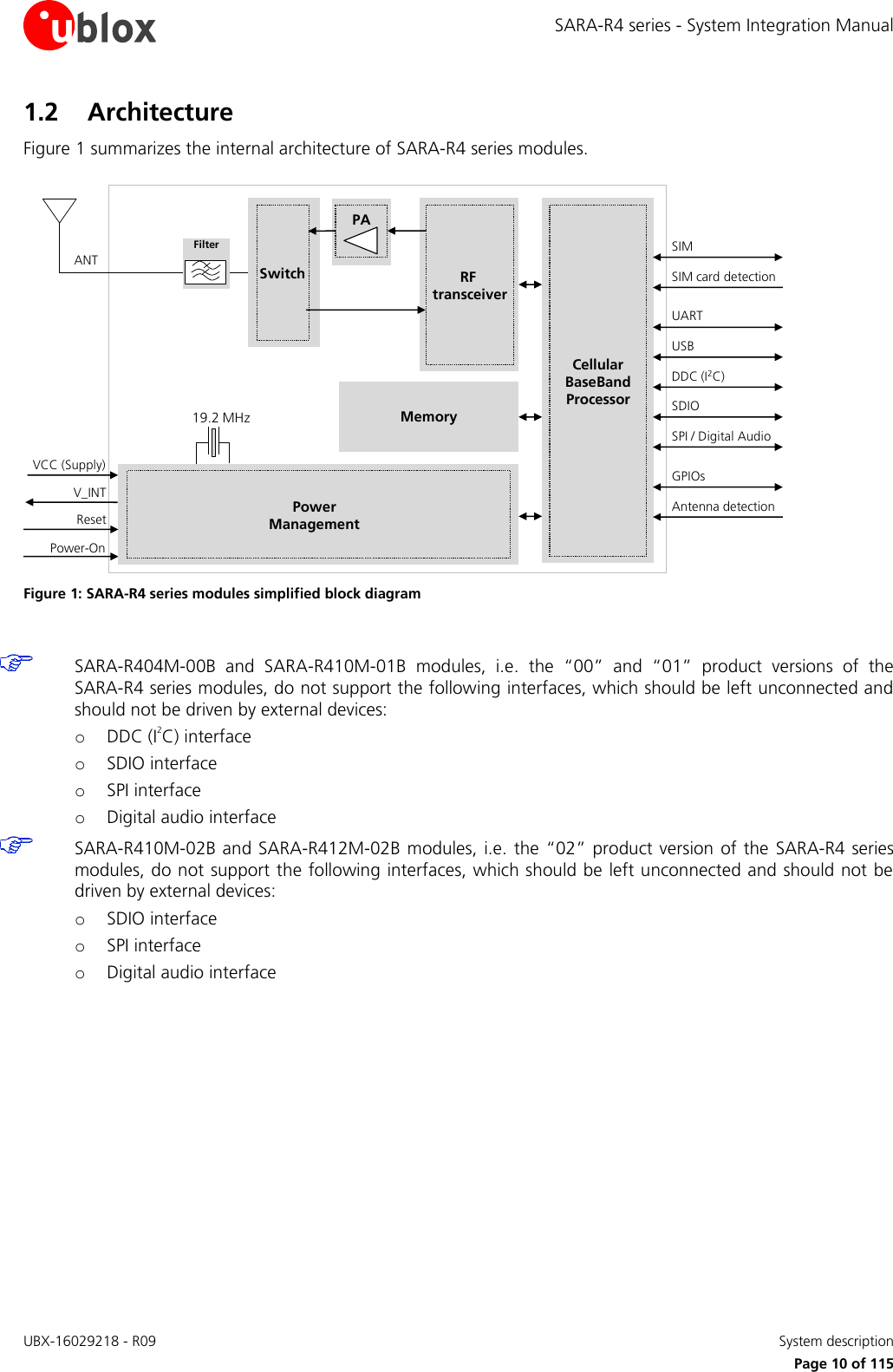
![SARA-R4 series - System Integration Manual UBX-16029218 - R09 System description Page 17 of 115 1.5 Supply interfaces 1.5.1 Module supply input (VCC) The modules must be supplied via the three VCC pins that represent the module power supply input. Voltage must be stable, because during operation, the current drawn by the SARA-R4 series modules through the VCC pins can vary by several orders of magnitude, depending on the operating mode and state (as described in sections 1.5.1.2, 1.5.1.3, 1.5.1.4 and 1.5.1.5). It is important that the supply source is able to withstand both the maximum pulse current occurring during a transmit burst at maximum power level and the average current consumption occurring during Tx / Rx call at maximum RF power level (see the SARA-R4 Data Sheet [1]). SARA-R412M modules provide separate supply inputs over the three VCC pins: VCC pins #52 and #53 represent the supply input for the internal RF power amplifier, demanding most of the total current drawn of the module when RF transmission is enabled during a call VCC pin #51 represents the supply input for the internal baseband Power Management Unit, demanding minor part of the total current drawn of the module when RF transmission is enabled during a call The three VCC pins of SARA-R404M and SARA-R410M modules are internally connected each other to both the internal RF Power Amplifier and the internal baseband Power Management Unit. Figure 3 provide a simplified block diagram of SARA-R4 series modules’ internal VCC supply routing. 53VCC52VCC51VCCSARA-R404M / SARA-R410MPower ManagementUnitMemoryBaseband ProcessorTransceiverPower Amplifier53VCC52VCC51VCCSARA-R412MPower ManagementUnitMemoryBaseband ProcessorTransceiverPower Amplifier Figure 3: Block diagram of SARA-R4 series modules’ internal VCC supply routing](https://usermanual.wiki/u-blox/2AGQN4NNN.User-Manual-2/User-Guide-3940431-Page-17.png)
![SARA-R4 series - System Integration Manual UBX-16029218 - R09 System description Page 18 of 115 1.5.1.1 VCC supply requirements Table 6 summarizes the requirements for the VCC modules supply. See section 2.2.1 for suggestions to correctly design a VCC supply circuit compliant with the requirements listed in Table 6. The supply circuit affects the RF compliance of the device integrating SARA-R4 series modules with applicable required certification schemes as well as antenna circuit design. Compliance is guaranteed if the requirements summarized in the Table 6 are fulfilled. Item Requirement Remark VCC nominal voltage Within VCC normal operating range: SARA-R404M /-R410M: 3.2 V / 4.2 V SARA-R412M: 3.2 V / 4.5 V RF performance is guaranteed when VCC voltage is inside the normal operating range limits. RF performance may be affected when VCC voltage is outside the normal operating range limits, though the module is still fully functional until the VCC voltage is inside the extended operating range limits. VCC voltage during normal operation Within VCC extended operating range: SARA-R404M /-R410M: 3.0 V / 4.2 V SARA-R412M: 3.0 V / 4.5 V VCC voltage must be above the extended operating range minimum limit to switch-on the module. The module may switch-off when the VCC voltage drops below the extended operating range minimum limit. Operation above VCC extended operating range is not recommended and may affect device reliability. VCC average current Support with adequate margin the highest averaged VCC current consumption value in connected mode conditions specified in the SARA-R4 Data Sheet [1] The maximum average current consumption can be greater than the specified value according to the actual antenna mismatching, temperature and supply voltage. Section 1.5.1.2 describes current consumption profiles in connected mode. VCC peak current Support with adequate margin the highest peak VCC current consumption value in Tx connected mode conditions specified in the SARA-R4 Data Sheet [1] The maximum peak Tx current consumption can be greater than the specified value according to the actual antenna mismatching, temperature and supply voltage. Section 1.5.1.2 describes current consumption profiles in connected mode. VCC voltage drop during Tx slots Lower than 400 mV VCC voltage drop directly affects the RF compliance with applicable certification schemes. Figure 6 describes VCC voltage drop during 2G Tx slots. VCC voltage ripple during Tx Noise in the supply pins must be minimized High supply voltage ripple values during RF transmissions in connected mode directly affect the RF compliance with the applicable certification schemes. VCC under/over-shoot at start/end of Tx slots Absent or at least minimized VCC under/over-shoot directly affects the RF compliance with applicable certification schemes. Figure 6 describes VCC voltage under/over-shoot. Table 6: Summary of VCC modules supply requirements](https://usermanual.wiki/u-blox/2AGQN4NNN.User-Manual-2/User-Guide-3940431-Page-18.png)
![SARA-R4 series - System Integration Manual UBX-16029218 - R09 System description Page 19 of 115 1.5.1.2 VCC current consumption in LTE connected mode During an LTE connection, the SARA-R4 series modules transmit and receive in half duplex mode. The current consumption depends on output RF power, which is always regulated by the network (the current base station) sending power control commands to the module. These power control commands are logically divided into a slot of 0.5 ms (time length of one Resource Block), thus the rate of power change can reach a maximum rate of 2 kHz. Figure 4 shows an example of SARA-R4 modules’ current consumption profile versus time in connected mode: transmission is enabled for one sub-frame (1 ms) according to LTE Category M1 half-duplex connected mode. Detailed current consumption values can be found in the SARA-R4 series Data Sheet [1]. Time [ms]Current [mA]0300200100500400Current consumption value depends on TX power and actual antenna load1 Slot1 Resource Block (0.5 ms) 1 LTE Radio Frame (10 ms)1 Slot1 Resource Block (0.5 ms) 1 LTE Radio Frame (10 ms) Figure 4: VCC current consumption profile versus time during LTE Cat M1 half-duplex connection](https://usermanual.wiki/u-blox/2AGQN4NNN.User-Manual-2/User-Guide-3940431-Page-19.png)
![SARA-R4 series - System Integration Manual UBX-16029218 - R09 System description Page 20 of 115 1.5.1.3 VCC current consumption in 2G connected mode When a GSM call is established, the VCC consumption is determined by the current consumption profile typical of the GSM transmitting and receiving bursts. The current consumption peak during a transmission slot is strictly dependent on the transmitted power, which is regulated by the network. The transmitted power in the transmit slot is also the more relevant factor for determining the average current consumption. If the module is transmitting in 2G single-slot mode (as in GSM talk mode) in the 850 or 900 MHz bands at the maximum RF power control level (approximately 2 W or 33 dBm in the Tx slot/burst), then the current consumption can reach a high peak / pulse (see the SARA-R4 series Data Sheet [1]) for 576.9 µs (width of the transmit slot/burst) with a periodicity of 4.615 ms (width of 1 frame = 8 slots/burst), that is, with a 1/8 duty cycle according to GSM TDMA (Time Division Multiple Access). If the module is transmitting in 2G single-slot mode in the 1800 or 1900 MHz bands, the current consumption figures are much lower than during transmission in the low bands, due to the 3GPP transmitter output power specifications. During a GSM call, current consumption is not significantly high while receiving or in monitor bursts, and it is low in the bursts unused to transmit / receive. Figure 5 shows an example of the module current consumption profile versus time in GSM talk mode. Time [ms]RX slotunused slotunused slotTX slotunused slotunused slotMON slotunused slotRX slotunused slotunused slotTX slotunused slotunused slotMON slotunused slotGSM frame 4.615 ms (1 frame = 8 slots)Current [A]200 mA60-120 mA1900 mAPeak current depends on TX power and actual antenna loadGSM frame 4.615 ms (1 frame = 8 slots)1.51.00.50.02.060-120 mA10-40 mA Figure 5: VCC current consumption profile versus time during a GSM call (1 TX slot, 1 RX slot) Figure 6 illustrates the VCC voltage profile versus time during a GSM call, according to the related VCC current consumption profile described in Figure 5 TimeundershootovershootrippledropVoltage3.8 V (typ)RX slotunused slotunused slotTX slotunused slotunused slotMON slotunused slotRX slotunused slotunused slotTX slotunused slotunused slotMON slotunused slotGSM frame 4.615 ms (1 frame = 8 slots)GSM frame 4.615 ms (1 frame = 8 slots) Figure 6: Description of the VCC voltage profile versus time during a GSM call (1 TX slot, 1 RX slot)](https://usermanual.wiki/u-blox/2AGQN4NNN.User-Manual-2/User-Guide-3940431-Page-20.png)
![SARA-R4 series - System Integration Manual UBX-16029218 - R09 System description Page 21 of 115 When a GPRS connection is established, more than one slot can be used to transmit and/or more than one slot can be used to receive. The transmitted power depends on network conditions, which set the peak current consumption. But according to GPRS specifications, the maximum transmitted RF power is reduced if more than one slot is used to transmit, so the maximum peak of current is not as high as it can be in the case of a GSM call. If the module transmits in GPRS multi-slot class 12, in 850 or 900 MHz bands, at maximum RF power level, the consumption can reach a quite a high peak but lower than the one achievable in 2G single-slot mode. This happens for 2.308 ms (width of the 4 Tx slots/bursts) in the case of multi-slot class 12, with a periodicity of 4.615 ms (width of 1 frame = 8 slots/bursts), so with a 1/2 duty cycle, according to GSM TDMA. If the module is in GPRS connected mode in the 1800 or 1900 MHz bands, consumption figures are lower than in the 850 or 900 MHz band because of the 3GPP Tx power specifications. Figure 7 illustrates the current consumption profiles in GPRS connected mode, in the 850 or 900 MHz bands, with 4 slots used to transmit and 1 slot used to receive, as for the GPRS multi-slot class 12. Time [ms]RX slotunused slotTX slotTX slotTX slotTX slotMON slotunused slotRX slotunused slotTX slotTX slotTX slotTX slotMON slotunused slotGSM frame 4.615 ms (1 frame = 8 slots)Current [A]60-120mAGSM frame 4.615 ms (1 frame = 8 slots)1.51.00.50.060-120mA10-40mA200mAPeak current depends on TX power and actual antenna load1600 mA Figure 7: VCC current consumption profile versus time during a GPRS multi-slot class 12 connection (4 TX slots, 1 RX slot) In case of EGPRS (i.e. EDGE) connections, the VCC current consumption profile is very similar to the one during GPRS connections: the current consumption profile in GPRS multi-slot class 12 connected mode illustrated in the Figure 7 is representative for the EDGE multi-slot class 12 connected mode as well. 1.5.1.4 VCC current consumption in low power deep sleep mode (power saving enabled) The power saving configuration is by default disabled, but it can be enabled using the AT+CPSMS command (see the SARA-R4 series AT Commands Manual [2] and section 1.13.9). When power saving is enabled, the module automatically enters the PSM low power deep sleep mode whenever possible, reducing current consumption down to a steady value in the µA range: only the RTC runs with internal 32 kHz reference clock frequency. Detailed current consumption values can be found in the SARA-R4 series Data Sheet [1]. Due to RTC running during PSM mode, the Cal-RC turns on the crystal every ~10 s to calibrate the RC oscillator, as a consequence, a very low spike in current consumption will be observed.](https://usermanual.wiki/u-blox/2AGQN4NNN.User-Manual-2/User-Guide-3940431-Page-21.png)
![SARA-R4 series - System Integration Manual UBX-16029218 - R09 System description Page 22 of 115 1.5.1.5 VCC current consumption in active mode (power saving disabled) The active mode is the state where the module is switched on and ready to communicate with an external device by means of the application interfaces (as the USB or the UART serial interface). The module processor core is active, and the 19.2 MHz reference clock frequency is used. If power saving configuration is disabled, as it is by default (see the SARA-R4 series AT Commands Manual [2], +CPSMS AT command for details), the module does not automatically enter the PSM low power deep sleep mode whenever possible: the module remains in active mode. Otherwise, if the power saving configuration is enabled, the module enters PSM low power deep sleep mode whenever possible (see section 1.13.9). Figure 8 illustrates a typical example of the module current consumption profile when the module is in active mode. In such case, the module is registered with the network and, while active mode is maintained, the receiver is periodically activated to monitor the paging channel for paging block reception. Detailed current consumption values can be found in the SARA-R4 series Data Sheet [1]. ACTIVE MODEPaging periodTime [s]Current [mA]Time [ms]Current [mA]RX Enabled01000100 Figure 8: VCC current consumption profile with power saving disabled and module registered with the network: active mode is always held and the receiver is periodically activated to monitor the paging channel for paging block reception 1.5.2 Generic digital interfaces supply output (V_INT) The V_INT output pin of the SARA-R4 series modules is generated by the module internal power management circuitry when the module is switched on and it is not in the deep sleep power saving mode. The typical operating voltage is 1.8 V, whereas the current capability is specified in the SARA-R4 series Data Sheet [1]. The V_INT voltage domain can be used in place of an external discrete regulator as a reference voltage rail for external components.](https://usermanual.wiki/u-blox/2AGQN4NNN.User-Manual-2/User-Guide-3940431-Page-22.png)
![SARA-R4 series - System Integration Manual UBX-16029218 - R09 System description Page 23 of 115 1.6 System function interfaces 1.6.1 Module power-on When the SARA-R4 series modules are in the not-powered mode (i.e. the VCC module supply is not applied), they can be switched on as follows: Rising edge on the VCC input pins to a valid voltage level, and then a low logic level needs to be set at the PWR_ON input pin for a valid time. When the SARA-R4 series modules are in the power-off mode (i.e. switched off) or in the PSM low power mode, with a valid VCC supply applied, they can be switched on as follows: Low pulse on the PWR_ON pin for a valid time period The PWR_ON input pin is equipped with an internal active pull-up resistor. Detailed electrical characteristics with voltages and timings are described in the SARA-R4 series Data Sheet [1]. Figure 9 shows the module switch-on sequence from the not-powered mode, describing the following phases: The external power supply is applied to the VCC module pins The PWR_ON pin is held low for a valid time All the generic digital pins of the module are tri-stated until the switch-on of their supply source (V_INT). The internal reset signal is held low: the baseband core and all the digital pins are held in the reset state. When the internal reset signal is released, any digital pin is set in the correct sequence from the reset state to the default operational configured state. The duration of this pins’ configuration phase differs within generic digital interfaces and the USB interface due to host / device enumeration timings (see section 1.9.2). The module is fully ready to operate after all interfaces are configured. VCCPWR_ONRESET_NV_INTInternal ResetGPIOSystem StateBB Pads State OperationalOFFONInternal Reset → OperationalTristate / Floating Internal ResetStart of interface configurationModule interfaces are configuredStart-up event~4.5 s0 s Figure 9: SARA-R4 series switch-on sequence description The Internal Reset signal is not available on a module pin, but it is recommended to monitor: the V_INT pin, to sense the start of the SARA-R4 series module switch-on sequence the GPIO pin configured to provide the module operating status indication (see the SARA-R4 series AT Commands Manual [2], AT+UGPIOC command), to sense when the module is ready to operate Before the switch-on of the generic digital interface supply source (V_INT) of the module, no voltage driven by an external application should be applied to any generic digital interface of the module. Before the SARA-R4 series module is fully ready to operate, the host application processor should not send any AT command over the AT communication interfaces (USB, UART) of the module. The duration of the SARA-R4 series modules’ switch-on routine can vary depending on the application / network settings and the concurrent module activities.](https://usermanual.wiki/u-blox/2AGQN4NNN.User-Manual-2/User-Guide-3940431-Page-23.png)
![SARA-R4 series - System Integration Manual UBX-16029218 - R09 System description Page 24 of 115 1.6.2 Module power-off SARA-R4 series can be cleanly switched off by: AT+CPWROFF command (see the SARA-R4 series AT Commands Manual [2]). The current parameter settings are saved in the module’s non-volatile memory and a clean network detach is performed. Low pulse on the PWR_ON pin for a valid time period (see the SARA-R4 series Data Sheet [1]). An abrupt under-voltage shutdown occurs on SARA-R4 series modules when the VCC module supply is removed. If this occurs, it is not possible to perform the storing of the current parameter settings in the module’s non-volatile memory or to perform the clean network detach. It is highly recommended to avoid an abrupt removal of the VCC supply during SARA-R4 series modules normal operations. An abrupt hardware shutdown occurs on SARA-R4 series modules when a low level is applied on RESET_N pin. In this case, the current parameter settings are not saved in the module’s non-volatile memory and a clean network detach is not performed. It is highly recommended to avoid an abrupt hardware shutdown of the module by forcing a low level on the RESET_N input pin during module normal operation: the RESET_N line should be set low only if reset or shutdown via AT commands fails or if the module does not reply to a specific AT command after a time period longer than the one defined in the SARA-R4 series AT Commands Manual [2]. Figure 10 describes the SARA-R4 series modules switch-off sequence started by means of the AT+CPWROFF command, allowing storage of current parameter settings in the module’s non-volatile memory and a clean network detach, with the following phases: When the +CPWROFF AT command is sent, the module starts the switch-off routine. The module replies OK on the AT interface: the switch-off routine is in progress. At the end of the switch-off routine, all the digital pins are tri-stated and all the internal voltage regulators are turned off, including the generic digital interfaces supply (V_INT). Then, the module remains in switch-off mode as long as a switch on event does not occur (e.g. applying a low level to PWR_ON), and enters not-powered mode if the supply is removed from the VCC pins. VCC PWR_ONRESET_N V_INTInternal ResetSystem StateBB Pads State OperationalOFFTristate / FloatingONOperational → TristateAT+CPWROFFsent to the moduleOKreplied by the moduleVCC can be removed Figure 10: SARA-R4 series switch-off sequence by means of AT+CPWROFF command The Internal Reset signal is not available on a module pin, but it is recommended to monitor the V_INT pin to sense the end of the switch-off sequence: VCC supply can be removed only after V_INT goes low. The duration of each phase in the SARA-R4 series modules’ switch-off routines can largely vary depending on the application / network settings and the concurrent module activities.](https://usermanual.wiki/u-blox/2AGQN4NNN.User-Manual-2/User-Guide-3940431-Page-24.png)
![SARA-R4 series - System Integration Manual UBX-16029218 - R09 System description Page 25 of 115 Figure 11 describes the SARA-R4 series modules switch-off sequence started by means of the PWR_ON input pin, allowing storage of current parameter settings in the module’s non-volatile memory and a clean network detach, with the following phases: A low pulse with appropriate time duration (see the SARA-R4 series Data Sheet [1]) is applied at the PWR_ON input pin. At the end of the switch-off routine, all the digital pins are tri-stated and all the internal voltage regulators are turned off, including the generic digital interfaces supply (V_INT). Then, the module remains in power-off mode as long as a switch on event does not occur (e.g. applying an appropriate low level to the PWR_ON input), and enters not-powered mode if the VCC supply is removed. VCC PWR_ONRESET_N V_INTInternal ResetSystem StateBB Pads StateOFFTristate / FloatingONOperational -> TristateOperational0 s~2.5 s~5 sThe module starts the switch-off routineVCC can be removed Figure 11: SARA-R4 series switch-off sequence by means of PWR_ON pin The Internal Reset signal is not available on a module pin, but it is recommended to monitor the V_INT pin to sense the end of the switch-off sequence: VCC supply can be removed only after V_INT goes low. The duration of each phase in the SARA-R4 series modules’ switch-off routines can largely vary depending on the application / network settings and the concurrent module activities. 1.6.3 Module reset SARA-R4 series modules can be cleanly reset (rebooted) by: AT+CFUN command (see the SARA-R4 series AT Commands Manual [2]). In the case listed above an “internal” or “software” reset of the module is executed: the current parameter settings are saved in the module’s non-volatile memory and a clean network detach is performed. An abrupt hardware shutdown occurs on SARA-R4 series modules when a low level is applied on RESET_N input pin for a valid time period. In this case, the current parameter settings are not saved in the module’s non-volatile memory and a clean network detach is not performed. Then, the module remains in power-off mode as long as a switch on event does not occur applying an appropriate low level to the PWR_ON input. It is highly recommended to avoid an abrupt hardware shutdown of the module by forcing a low level on the RESET_N input during modules normal operation: the RESET_N line should be set low only if reset or shutdown via AT commands fails or if the module does not provide a reply to a specific AT command after a time period longer than the one defined in the SARA-R4 series AT Commands Manual [2]. The RESET_N input pin is equipped with an internal pull-up to a 1.8 V supply domain. Detailed electrical characteristics with voltages and timings are described in the SARA-R4 series Data Sheet [1].](https://usermanual.wiki/u-blox/2AGQN4NNN.User-Manual-2/User-Guide-3940431-Page-25.png)
![SARA-R4 series - System Integration Manual UBX-16029218 - R09 System description Page 26 of 115 1.7 Antenna interface 1.7.1 Antenna RF interface (ANT) SARA-R4 series modules provide an RF interface for connecting the external antenna. The ANT pin represents the primary RF input/output for transmission and reception of LTE RF signals. The ANT pin has a nominal characteristic impedance of 50 and must be connected to the primary Tx / Rx antenna through a 50 transmission line to allow clear RF transmission and reception. 1.7.1.1 Antenna RF interfaces requirements Table 7 summarizes the requirements for the antenna RF interface. See section 2.4.1 for suggestions to correctly design antennas circuits compliant with these requirements. The antenna circuits affect the RF compliance of the device integrating SARA-R4 series modules with applicable required certification schemes (for more details see section 4). Compliance is guaranteed if the antenna RF interface requirements summarized in Table 7 are fulfilled. Item Requirements Remarks Impedance 50 nominal characteristic impedance The impedance of the antenna RF connection must match the 50 impedance of the ANT port. Frequency Range See the SARA-R4 series Data Sheet [1] The required frequency range of the antenna connected to ANT port depends on the operating bands of the used cellular module and the used mobile network. Return Loss S11 < -10 dB (VSWR < 2:1) recommended S11 < -6 dB (VSWR < 3:1) acceptable The Return loss or the S11, as the VSWR, refers to the amount of reflected power, measuring how well the antenna RF connection matches the 50 characteristic impedance of the ANT port. The impedance of the antenna termination must match as much as possible the 50 nominal impedance of the ANT port over the operating frequency range, reducing as much as possible the amount of reflected power. Efficiency > -1.5 dB ( > 70% ) recommended > -3.0 dB ( > 50% ) acceptable The radiation efficiency is the ratio of the radiated power to the power delivered to antenna input: the efficiency is a measure of how well an antenna receives or transmits. The radiation efficiency of the antenna connected to the ANT port needs to be enough high over the operating frequency range to comply with the Over-The-Air (OTA) radiated performance requirements, as Total Radiated Power (TRP) and the Total Isotropic Sensitivity (TIS), specified by applicable related certification schemes. Maximum Gain According to radiation exposure limits The power gain of an antenna is the radiation efficiency multiplied by the directivity: the gain describes how much power is transmitted in the direction of peak radiation to that of an isotropic source. The maximum gain of the antenna connected to ANT port must not exceed the herein stated value to comply with regulatory agencies radiation exposure limits. For additional info see sections 4.2.2. Input Power > 24 dBm ( > 0.25 W ) for R404M / R410M > 33 dBm ( > 2.0 W ) for R412M The antenna connected to the ANT port must support with adequate margin the maximum power transmitted by the modules. Table 7: Summary of Tx/Rx antenna RF interface requirements](https://usermanual.wiki/u-blox/2AGQN4NNN.User-Manual-2/User-Guide-3940431-Page-26.png)
![SARA-R4 series - System Integration Manual UBX-16029218 - R09 System description Page 27 of 115 1.7.2 Antenna detection interface (ANT_DET) The antenna detection is based on ADC measurement. The ANT_DET pin is an Analog to Digital Converter (ADC) provided to sense the antenna presence. The antenna detection function provided by ANT_DET pin is an optional feature that can be implemented if the application requires it. The antenna detection is forced by the +UANTR AT command. See the SARA-R4 series AT Commands Manual [2] for more details on this feature. The ANT_DET pin generates a DC current (for detailed characteristics see the SARA-R4 series Data Sheet [1]) and measures the resulting DC voltage, thus determining the resistance from the antenna connector provided on the application board to GND. So, the requirements to achieve antenna detection functionality are the following: an RF antenna assembly with a built-in resistor (diagnostic circuit) must be used an antenna detection circuit must be implemented on the application board See section 2.4.2 for antenna detection circuit on application board and diagnostic circuit on antenna assembly design-in guidelines. 1.8 SIM interface 1.8.1 SIM interface SARA-R4 series modules provide high-speed SIM/ME interface including automatic detection and configuration of the voltage required by the connected SIM card or chip. Both 1.8 V and 3 V SIM types are supported. Activation and deactivation with automatic voltage switch from 1.8 V to 3 V are implemented, according to ISO-IEC 7816-3 specifications. The VSIM supply output provides internal short circuit protection to limit start-up current and protect the SIM to short circuits. The SIM driver supports the PPS (Protocol and Parameter Selection) procedure for baud-rate selection, according to the values determined by the SIM card or chip. 1.8.2 SIM detection interface The GPIO5 pin is configured as an external interrupt to detect the SIM card mechanical / physical presence. The pin is configured as input with an internal active pull-down enabled, and it can sense SIM card presence only if cleanly connected to the mechanical switch of a SIM card holder as described in section 2.5: Low logic level at GPIO5 input pin is recognized as SIM card not present High logic level at GPIO5 input pin is recognized as SIM card present For more details, see the SARA-R4 series AT Commands Manual [2], +UGPIOC, +CIND and +CMER AT commands.](https://usermanual.wiki/u-blox/2AGQN4NNN.User-Manual-2/User-Guide-3940431-Page-27.png)
![SARA-R4 series - System Integration Manual UBX-16029218 - R09 System description Page 28 of 115 1.9 Data communication interfaces SARA-R4 series modules provide the following serial communication interface: UART interface: Universal Asynchronous Receiver/Transmitter serial interface available for the communication with a host application processor (AT commands, data, FW update by means of FOAT). See section 1.9.1. USB interface: Universal Serial Bus 2.0 compliant interface available for the communication with a host application processor (AT commands, data, FW update by means of the FOAT feature), for FW update by means of the u-blox dedicated tool and for diagnostics. See section 1.9.2. SPI interface: Serial Peripheral Interface available for communication with an external compatible device. See section 1.9.3. SDIO interface: Secure Digital Input Output interface available for communication with a compatible device. See section 1.9.4. DDC interface: I2C bus compatible interface available for the communication with u-blox GNSS positioning chips or modules and with external I2C devices. See section 1.9.5. 1.9.1 UART interface 1.9.1.1 UART features The UART interface is a 9-wire 1.8 V unbalanced asynchronous serial interface available on all the SARA-R4 series modules, supporting: AT command mode3 Data mode and Online command mode3 Multiplexer protocol functionality FW upgrades by means of the FOAT feature (see 1.13.7) The UART is available only if the USB is not enabled as AT command / data communication interface: UART and USB cannot be concurrently used for this purpose. UART interface provides RS-232 functionality conforming to the ITU-T V.24 Recommendation [5], with CMOS compatible signal levels: 0 V for low data bit or ON state, and 1.8 V for high data bit or OFF state (for detailed electrical characteristics see the SARA-R4 series Data Sheet [1]), providing: data lines (RXD as output, TXD as input) hardware flow control lines (CTS as output, RTS as input) modem status and control lines (DTR as input, DSR as output, DCD as output, RI as output) SARA-R4 series modules are designed to operate as cellular modems, i.e. as the data circuit-terminating equipment (DCE) according to the ITU-T V.24 Recommendation [5]. A host application processor connected to the module through the UART interface represents the data terminal equipment (DTE). UART signal names of the cellular modules conform to the ITU-T V.24 Recommendation [5]: e.g. TXD line represents data transmitted by the DTE (host processor output) and received by the DCE (module input). Hardware flow control is not supported by the “00”, “01” and SARA-R410M-02B product versions, but the RTS input line of the module must be set low (= ON state) to communicate over UART interface on the “00” and “01” product versions. DTR input of the module must be set low (= ON state) to have URCs presented over UART interface. 3 For the definition of the interface data mode, command mode and online command mode see SARA-R4 series AT Commands Manual [1]](https://usermanual.wiki/u-blox/2AGQN4NNN.User-Manual-2/User-Guide-3940431-Page-28.png)
![SARA-R4 series - System Integration Manual UBX-16029218 - R09 System description Page 29 of 115 SARA-R4 series modules’ UART interface is by default configured in AT command mode, if the USB interface is not enabled as AT command / data communication interface (UART and USB cannot be concurrently used for this purpose): the module waits for AT command instructions and interprets all the characters received as commands to execute. All the functionalities supported by SARA-R4 series modules can be in general set and configured by AT commands: AT commands according to 3GPP TS 27.007 [6], 3GPP TS 27.005 [7], 3GPP TS 27.010 [8] u-blox AT commands (for the complete list and syntax see the SARA-R4 series AT Commands Manual [2]) The default baud rate is 115200 b/s, while the default frame format is 8N1 (8 data bits, No parity, 1 stop bit: see Figure 12). Baud rates can be configured by AT command (see the SARA-R4 series AT Commands Manual [2]). The automatic baud rate detection and the automatic frame format recognition are not supported. D0 D1 D2 D3 D4 D5 D6 D7Start of 1-BytetransferStart Bit(Always 0)Possible Start ofnext transferStop Bit(Always 1)tbit = 1/(Baudrate)Normal Transfer, 8N1 Figure 12: Description of UART 8N1 frame format (8 data bits, no parity, 1 stop bit) 1.9.1.2 UART signals behavior At the end of the module boot sequence (see Figure 9), the module is by default in active mode, and the UART interface is initialized and enabled as AT commands interface only if the USB interface is not enabled as AT command / data communication interface: UART and USB cannot be concurrently used for this purpose. The configuration and the behavior of the UART signals after the boot sequence are described below: The module data output line (RXD) is set by default to the OFF state (high level) at UART initialization. The module holds RXD in the OFF state until the module transmits some data. The module data input line (TXD) is assumed to be controlled by the external host once UART is initialized and if UART is used in the application. The TXD data input line has an internal active pull-down enabled on the “00” and “02” product versions, and an internal active pull-up enabled on the “01” product version. UART multiplexer protocol SARA-R4 series modules include multiplexer functionality as per 3GPP TS 27.010 [8], on the UART physical link. This is a data link protocol which uses HDLC-like framing and operates between the module (DCE) and the application processor (DTE) and allows a number of simultaneous sessions over the used physical link (UART). The following virtual channels are defined: Channel 0: for Multiplexer control Channel 1: for all AT commands, and non-Dial Up Network (non-DUN) data connections. UDP, TCP data socket / data call connections via relevant AT commands. Channel 2: for Dial Up Network (DUN) data connection. It requires the host to have and use its own TCP/IP stack. The DUN can be initiated on the modem side or terminal/host side. Channel 3: for u-blox GNSS data tunneling (not supported by the “00” and “01” product versions).](https://usermanual.wiki/u-blox/2AGQN4NNN.User-Manual-2/User-Guide-3940431-Page-29.png)
![SARA-R4 series - System Integration Manual UBX-16029218 - R09 System description Page 30 of 115 1.9.2 USB interface 1.9.2.1 USB features SARA-R4 series modules include a High-Speed USB 2.0 compliant interface with 480 Mb/s maximum data rate, representing the main interface for transferring high speed data with a host application processor, supporting: AT command mode4 Data mode and Online command mode4 FW upgrades by means of the FOAT feature (see 1.13.7) FW upgrades by means of the u-blox dedicated tool Trace log capture (diagnostic purposes) The module itself acts as a USB device and can be connected to a USB host such as a Personal Computer or an embedded application microprocessor equipped with compatible drivers. The USB_D+/USB_D- lines carry USB serial bus data and signaling according to the Universal Serial Bus Revision 2.0 specification [4], while the VUSB_DET input pin senses the VBUS USB supply presence (nominally 5 V at the source) to detect the host connection and enable the interface. Neither the USB interface, nor the whole module is supplied by the VUSB_DET input, which senses the USB supply voltage and absorbs few microamperes. The USB interface is available as AT command / data communication interface only if an external valid USB VBUS supply voltage (5.0 V typical) is applied at the VUSB_DET input of the module since the switch-on of the module, and then held during normal operations. In this case, the UART will be not available. If the USB interface is enabled, the module does not enter the low power deep sleep mode: the external USB VBUS supply voltage needs to be removed from the VUSB_DET input of the module to let it enter the Power Saving Mode defined in 3GPP Rel.13. The USB interface is controlled and operated with: AT commands according to 3GPP TS 27.007 [6], 3GPP TS 27.005 [7] u-blox AT commands (for the complete list and syntax see the SARA-R4 series AT Commands Manual [2]) The USB interface of SARA-R4 series modules can provide the following USB functions: AT commands and data communication Diagnostic log The USB profile of SARA-R4 series modules identifies itself by the following VID (Vendor ID) and PID (Product ID) combination, included in the USB device descriptor according to the USB 2.0 specifications [4]. VID = 0x05C6 PID = 0x90B2 4 For the definition of the interface data mode, command mode and online command mode see SARA-R4 series AT Commands Manual [2]](https://usermanual.wiki/u-blox/2AGQN4NNN.User-Manual-2/User-Guide-3940431-Page-30.png)
![SARA-R4 series - System Integration Manual UBX-16029218 - R09 System description Page 31 of 115 1.9.3 SPI interface The SPI interface is not supported by “00”, “01” and “02” product versions: the SPI interface pins should not be driven by any external device. SARA-R4 series modules include a Serial Peripheral Interface for communication with compatible external device. The SPI interface can be made available as alternative function, in mutually exclusive way, over the digital audio interface pins (I2S_WA / SPI_MOSI, I2S_RXD / SPI_MISO, I2S_CLK / SPI_CLK, I2S_TXD / SPI_CS). 1.9.4 SDIO interface The SDIO interface is not supported by “00”, “01” and “02” product versions: the SDIO interface pins should not be driven by any external device. SARA-R4 series modules include a 4-bit Secure Digital Input Output interface (SDIO_D0, SDIO_D1, SDIO_D2, SDIO_D3, SDIO_CLK, SDIO_CMD) designed to communicate with external compatible SDIO devices. 1.9.5 DDC (I2C) interface The I2C interface is not supported by “00” and “01” product versions: the I2C interface pins should not be driven by any external device. SARA-R4 series modules include an I2C-bus compatible DDC interface (SDA, SCL) available to communicate with a u-blox GNSS receiver and with external I2C devices as an audio codec: the SARA-R4 module acts as an I2C master which can communicate with I2C slaves in accordance with the I2C bus specifications [9]. The SDA and SCL pins have internal pull-up to V_INT, so there is no need of additional pull-up resistors on the external application board. 1.10 Audio Audio is not supported by “00”, “01” and “02” product versions: the I2S interface pins should not be driven by any external device. SARA-R4 series modules support VoLTE (Voice over LTE Cat M1 radio bearer) for providing audio services. SARA-R4 series modules include an I2S digital audio interface to transfer digital audio data to/from an external compatible audio device. The digital audio interface can be made available as alternative function, in mutually exclusive way, over the SPI interface pins (I2S_WA / SPI_MOSI, I2S_RXD / SPI_MISO, I2S_CLK / SPI_CLK, I2S_TXD / SPI_CS).](https://usermanual.wiki/u-blox/2AGQN4NNN.User-Manual-2/User-Guide-3940431-Page-31.png)
![SARA-R4 series - System Integration Manual UBX-16029218 - R09 System description Page 32 of 115 1.11 General Purpose Input/Output SARA-R4 series modules include six pins (GPIO1-GPIO6) which can be configured as General Purpose Input/Output or to provide custom functions via u-blox AT commands (for more details see the SARA-R4 series AT Commands Manual [2], +UGPIOC, +UGPIOR, +UGPIOW AT commands), as summarized in Table 8. Function Description Default GPIO Configurable GPIOs Network status indication Network status: registered / data transmission, no service -- GPIO1 GNSS supply enable5 Enable/disable the supply of a u-blox GNSS receiver connected to the cellular module by the DDC (I2C) interface -- GPIO2 GNSS data ready5 Sense when a u-blox GNSS receiver connected to the module is ready for sending data by the DDC (I2C) interface -- GPIO3 SIM card detection SIM card physical presence detection -- GPIO5 Module status indication Module switched off or in PSM low power deep sleep mode, versus active or connected mode -- GPIO1, GPIO2, GPIO3, GPIO4, GPIO5, GPIO6 General purpose input Input to sense high or low digital level -- GPIO1, GPIO2, GPIO3, GPIO4, GPIO5, GPIO6 General purpose output Output to set the high or the low digital level -- GPIO1, GPIO2, GPIO3, GPIO4, GPIO6 Pin disabled Tri-state with an internal active pull-down enabled GPIO1, GPIO2, GPIO3, GPIO4, GPIO5, GPIO6 GPIO1, GPIO2, GPIO3, GPIO4, GPIO5, GPIO6 Table 8: SARA-R4 series GPIO custom functions configuration 1.12 Reserved pins (RSVD) SARA-R4 series modules have pins reserved for future use, marked as RSVD. All the RSVD pins are to be left unconnected on the application board, except for the RSVD pin number 33 that can be externally connected to ground. 5 Not supported by “00” and “01” product versions](https://usermanual.wiki/u-blox/2AGQN4NNN.User-Manual-2/User-Guide-3940431-Page-32.png)
![SARA-R4 series - System Integration Manual UBX-16029218 - R09 System description Page 33 of 115 1.13 System features 1.13.1 Network indication GPIOs can be configured by the AT command to indicate network status (for further details see section 1.11 and the SARA-R4 series AT Commands Manual [2]): No service (no network coverage or not registered) Registered / Data call enabled (RF data transmission / reception) 1.13.2 Antenna supervisor The antenna detection function provided by the ANT_DET pin is based on an ADC measurement as optional feature that can be implemented if the application requires it. The antenna supervisor is forced by the +UANTR AT command (see the SARA-R4 series AT Commands Manual [2] for more details). The requirements to achieve antenna detection functionality are the following: an RF antenna assembly with a built-in resistor (diagnostic circuit) must be used an antenna detection circuit must be implemented on the application board See section 1.7.2 for detailed antenna detection interface functional description and see section 2.4.2 for detection circuit on application board and diagnostic circuit on antenna assembly design-in guidelines. 1.13.3 Dual stack IPv4/IPv6 SARA-R4 series support both Internet Protocol version 4 and Internet Protocol version 6 in parallel. For more details about dual stack IPv4/IPv6 see the SARA-R4 series AT Commands Manual [2]. 1.13.4 TCP/IP and UDP/IP SARA-R4 series modules provide embedded TCP/IP and UDP/IP protocol stack: a PDP context can be configured established and handled via the data connection management packet switched data commands. SARA-R4 series modules provide Direct Link mode to establish a transparent end-to-end communication with an already connected TCP or UDP socket via serial interfaces (USB, UART). In Direct Link mode, data sent to the serial interface from an external application processor is forwarded to the network and vice-versa. For more details on embedded TCP/IP and UDP/IP functionalities, see SARA-R4 series AT Commands Manual [2]. 1.13.5 FTP SARA-R4 series provide embedded File Transfer Protocol (FTP) services. Files are read and stored in the local file system of the module. FTP files can also be transferred using FTP Direct Link: FTP download: data coming from the FTP server is forwarded to the host processor via USB / UART serial interfaces (for FTP without Direct Link mode the data is always stored in the module’s flash file system) FTP upload: data coming from the host processor via USB / UART serial interface is forwarded to the FTP server (for FTP without Direct Link mode the data is read from the module’s flash file system) When Direct Link is used for an FTP file transfer, only the file contents passes through USB / UART serial interface, whereas all the FTP command handling is managed internally by the FTP application. For more details about embedded FTP functionalities, see the SARA-R4 series AT Commands Manual [2].](https://usermanual.wiki/u-blox/2AGQN4NNN.User-Manual-2/User-Guide-3940431-Page-33.png)
![SARA-R4 series - System Integration Manual UBX-16029218 - R09 System description Page 34 of 115 1.13.6 HTTP SARA-R4 series modules provide the embedded Hypertext Transfer Protocol (HTTP) services via AT commands for sending requests to a remote HTTP server, receiving the server response and transparently storing it in the module’s flash file system. For more details, see the SARA-R4 series AT Commands Manual [2]. Firmware update Over AT (FOAT) This feature allows upgrading of the module firmware over the AT interface, using AT commands. The +UFWUPD AT command enables a code download to the device from the host via the Xmodem protocol. The +UFWINSTALL AT command then triggers a reboot, and upon reboot initiates a firmware installation on the device via a special boot loader on the module. The bootloader first authenticates the downloaded image, then installs it, and then reboots the module. Firmware authenticity verification is performed via a security signature. The firmware is then installed, overwriting the current version. In case of power loss during this phase, the boot loader detects a fault at the next wake-up, and restarts the firmware installation. After completing the upgrade, the module is reset again and wakes-up in normal boot. For more details about Firmware update Over AT procedure, see the SARA-R4 series AT Commands Manual [2], +UFWUPD AT command. 1.13.8 Firmware update Over The Air (uFOTA) This feature allows upgrading the module firmware over the air interface, based on u-blox client/server solution (uFOTA), using LWM2M. For more details about firmware update over-the-air procedure, see the SARA-R4 series AT Commands Manual [2]. 1.13.9 Power saving 1.13.9.1 Guidelines to optimize power consumption The LTE Cat M1 / NB1 technology is mainly intended for applications that only require a small amount of data exchange per day (i.e. a few bytes in uplink and downlink per day). Depending on the application type, the battery may be required to last for a few years. For these reasons, the whole application board should be optimized in terms of current consumption and should carefully take into account the following aspects: Enable the power saving mode configuration using the AT+CPSMS command (for the complete description of the AT+CPSMS command, see the SARA-R4 series AT Commands Manual [2]). Use the UART interface instead of the USB interface as a serial communication interface, because the current consumption of the module is ~20 mA higher when the USB interface is enabled. Use an application processor with a UART interface working at the same voltage level (1.8 V) as the module. In this way it is possible to avoid voltage translators, which helps to minimize current leakage. If the USB interface is implemented in the design, remove the external USB VBUS voltage from the VUSB_DET input when serial communication is not necessary, letting the module enter the Power Saving Mode defined in 3GPP Rel.13: the module does not enter the deep sleep power saving mode if the USB interface is enabled. Minimize current leakage on the power supply line. Optimize the antenna matching, since a mismatched antenna leads to higher current consumption. Monitor V_INT level to sense when the module enters power-off mode or deep sleep power saving mode. Disconnect the VCC supply source from the module when it is switched off (see 2.2.1.9). Disconnect the VCC supply source from the module during deep sleep power saving mode (see 2.2.1.9): using a host application processor equipped with a RTC, the module can execute a standard PSM procedure and](https://usermanual.wiki/u-blox/2AGQN4NNN.User-Manual-2/User-Guide-3940431-Page-34.png)
![SARA-R4 series - System Integration Manual UBX-16029218 - R09 System description Page 35 of 115 store the NAS protocol context in non-volatile memory, and then rely on the host application processor for running its RTC and triggering wake-up upon need6. 1.13.9.2 Functionality When power saving is enabled using the AT+CPSMS command, the module automatically enters the low power deep sleep mode whenever possible, reducing current consumption (see the section 1.5.1.4 and the SARA-R4 series Data Sheet [1]). For the definition and the description of the SARA-R4 series operating modes, including the events forcing transitions between the different operating modes, see section 1.4. The SARA-R4 series modules achieve the low power deep sleep mode by powering down all the Hardware components with the exception of the 32 kHz reference internally generated. From the host application point of view, the serial port will not be available during low power deep sleep mode, as the SARA-R4 module will act as if the SARA-R4 module is in Power-Off mode. 1.13.9.3 Timers and network interaction The SARA-R4 series modules goes in low power deep sleep mode entering in the Power Saving Mode (PSM) defined in 3GPP Release 13. Two timers have been specified on the PSM Signaling: the “Periodic Update Timer” and “Active Timer”. The “Active Timer” is the time defined by the network where the SARA-R4 series module will keep listening for any active operation, during this time the SARA-R4 series module is in Active mode. The “Periodic Update Timer” is the Extended Tracking Area Update (TAU) used by the SARA-R4 series module to periodically notify the network of its availability. The SARA-R4 series module requests the PSM by including the “Active Timer” with the desired value in the Attach, TAU or Routing Area Update (RAU) messages. The “Active Timer” is the time the module listens to the Paging Channel after having transitioned from connected to active mode. When the “Active Timer” expires, the module enters PSM low power deep sleep mode. SARA-R4 series module can also request an extended “Periodic Update Timer” value to remain in PSM low power deep sleep mode for longer than the original “Periodic Update Timer” broadcasted by the network. The grant of PSM is a negotiation between SARA-R4 series module and the attached network: the network accepts PSM by providing the actual value of the “Active Timer” (and “Periodic Update Timer”) to be used in the Attach/TAU/RAU accept procedure. The maximum duration, including the “Periodic Update Timer”, is about 413 days. The SARA-R4 series module enters PSM low power deep sleep mode only after the “Active Timer” expires. PSM low power deep sleep mode(periodic update timer)Connected mode: Data Tx / RxActive mode(active timer)TimeCurrent Figure 13: Description of the PSM timing 6 The use of an external RTC during deep sleep power saving mode is not supported by the “00”, “01” and “02” product versions](https://usermanual.wiki/u-blox/2AGQN4NNN.User-Manual-2/User-Guide-3940431-Page-35.png)
![SARA-R4 series - System Integration Manual UBX-16029218 - R09 System description Page 36 of 115 1.13.9.4 Timers and AT interaction The SARA-R4 series modules goes in low power deep sleep mode entering in the Power Saving Mode (PSM) only after the 6 s “AT Inactivity Timer” expires: If the UART interface is used, the host application has to stop sending AT commands for 6 s, consisting in the “AT Inactivity Timer” expiration, therefore allowing the module enter deep sleep power saving mode according to “Active Timer” expiration If the USB interface is enabled, the module does not enter the deep sleep power saving mode 1.13.9.5 AT commands The module uses the +CPSMS AT command with its defined parameters to request PSM timers to the network. See the SARA-R4 series AT Commands Manual [2] for details of the +CPSMS operation and features. 1.13.9.6 Host application The PSM low power deep sleep mode implementation allows the SARA-R4 series module to help extend the battery life of the application. The Host Application should be aware that the SARA-R4 series module is PSM-capable. The host application needs to sense the V_INT supply output of the module to get the notification when the module has entered into PSM low power deep sleep mode. If the host application receives an event that needs to be reported by the SARA-R4 series module interrupting the PSM low power deep sleep mode, it can be done so by setting the module into Active mode using the appropriate power-on event (see 1.6.1). From the host application point of view, the SARA-R4 module will look as it is in Power-Off mode. 1.13.9.7 Normal operation The Host Application can force the SARA-R4 series module to transition from PSM low power deep sleep mode to Active mode by using the Power-Up procedure specified in section 1.6.1. Be aware that when the host application transitions from low power deep sleep mode to active mode, it will cause the SARA-R4 series module to consume the same amount of power as in active mode, thereby shortening the battery life of the host application.](https://usermanual.wiki/u-blox/2AGQN4NNN.User-Manual-2/User-Guide-3940431-Page-36.png)
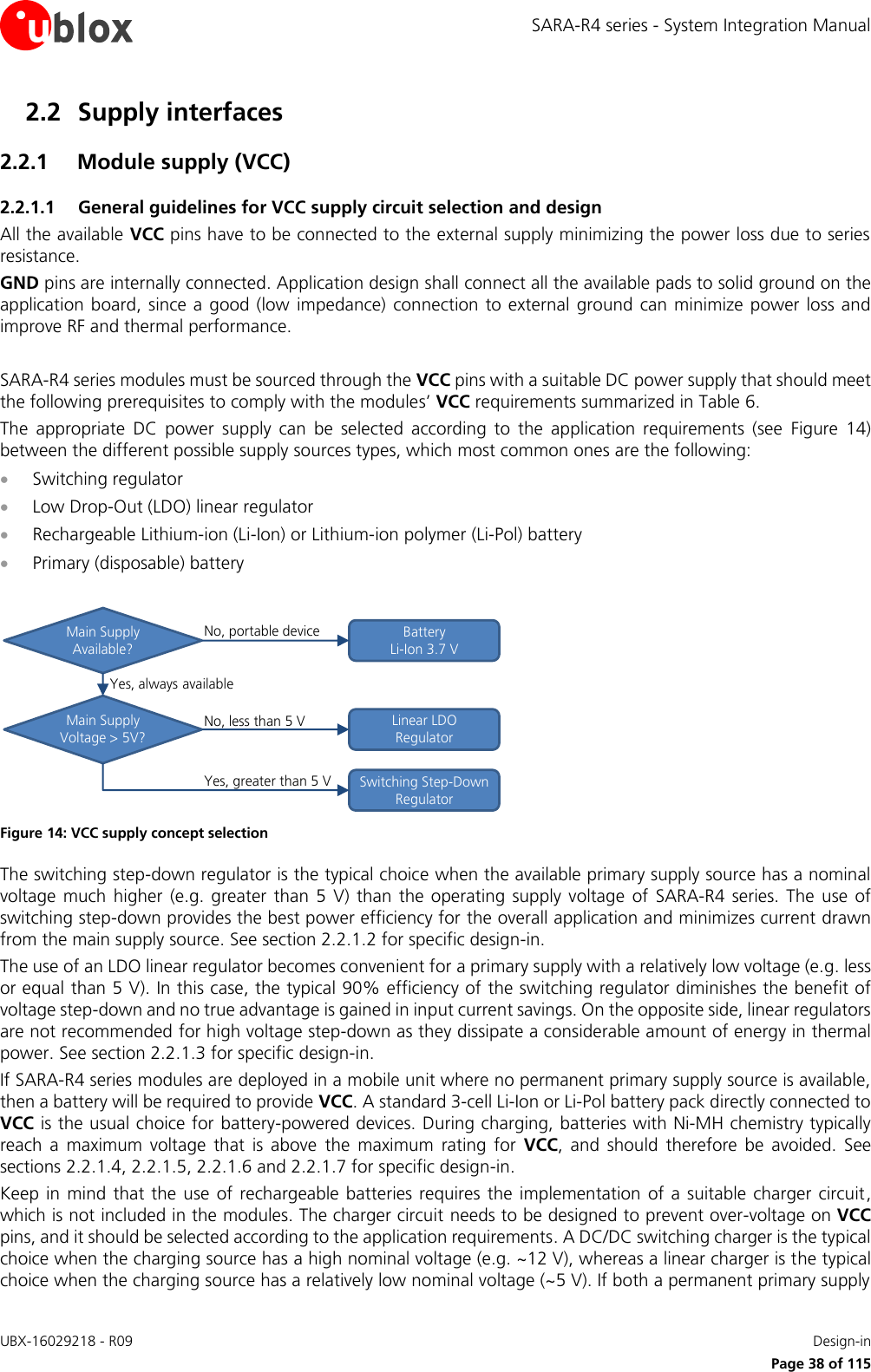
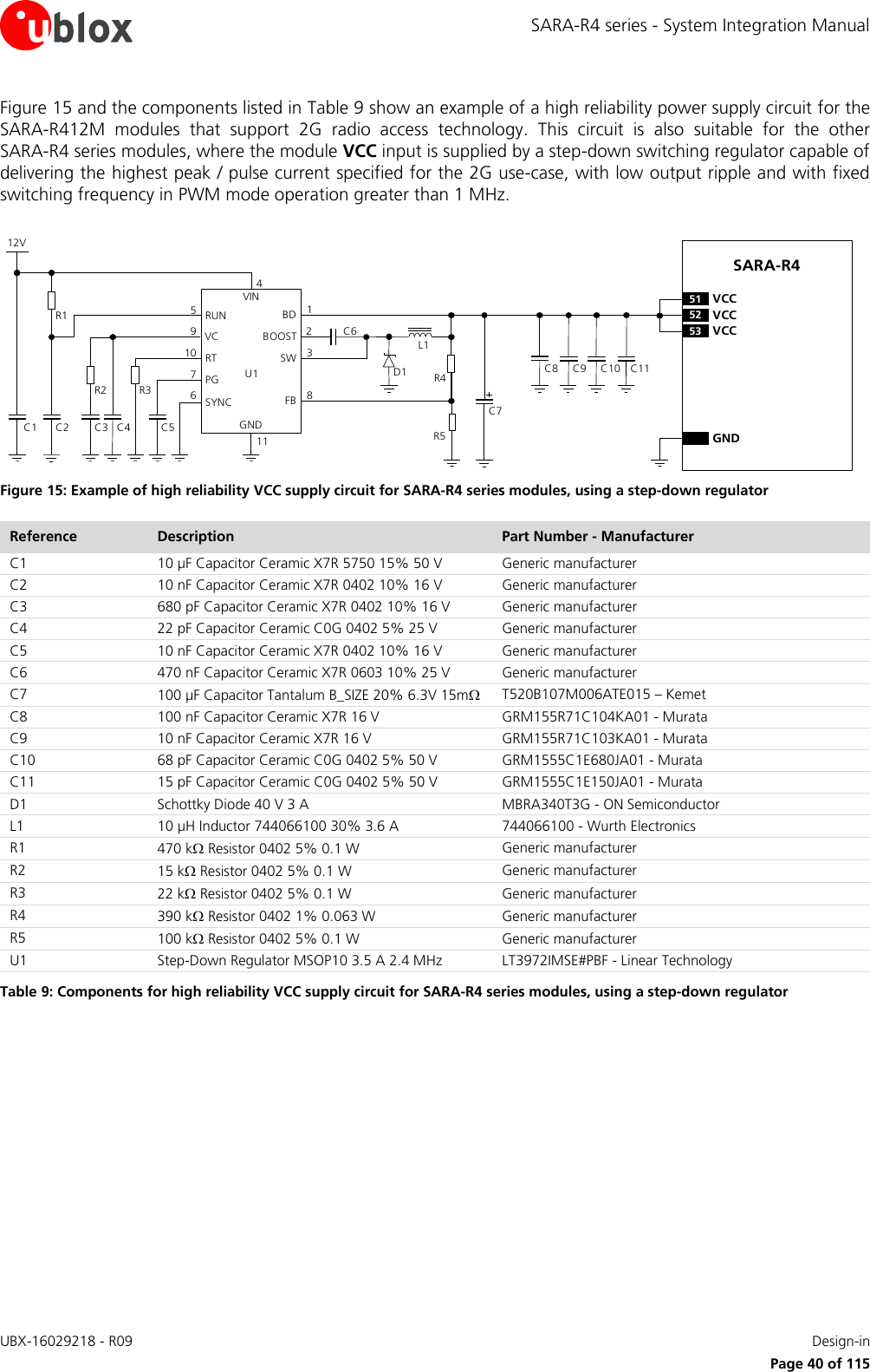
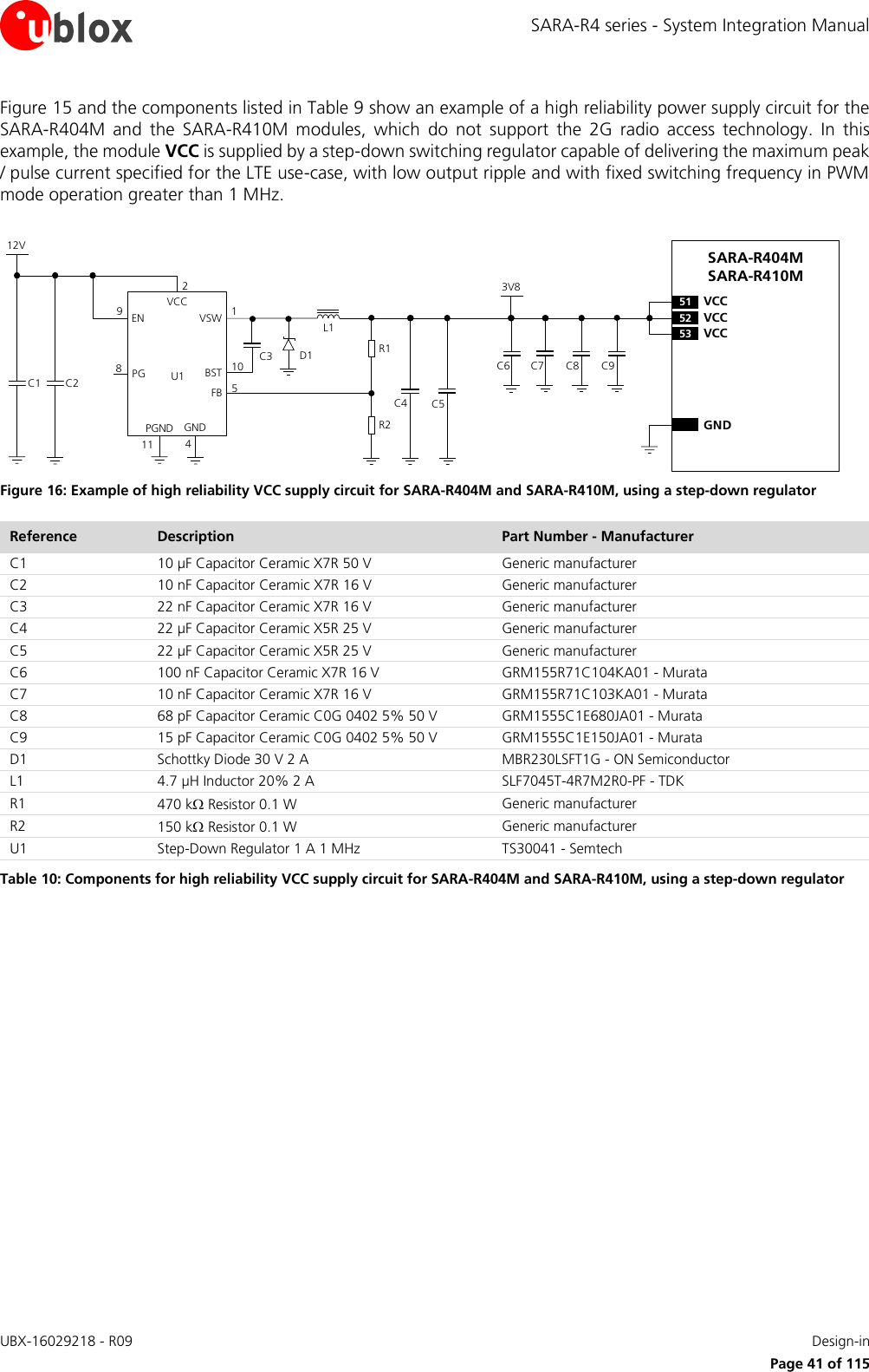
![SARA-R4 series - System Integration Manual UBX-16029218 - R09 Design-in Page 39 of 115 / charging source (e.g. ~12 V) and a rechargeable back-up battery (e.g. 3.7 V Li-Pol) are available at the same time as possible supply source, then a suitable charger / regulator with integrated power path management function can be selected to supply the module while simultaneously and independently charging the battery. See sections 2.2.1.6 and 2.2.1.7 for specific design-in. An appropriate primary (not rechargeable) battery can be selected taking into account the maximum current specified in the SARA-R4 series Data Sheet [1] during connected mode, considering that primary cells might have weak power capability. See section 2.2.1.5 for specific design-in. The usage of more than one DC supply at the same time should be carefully evaluated: depending on the supply source characteristics, different DC supply systems can result as mutually exclusive. The selected regulator or battery must be able to support with adequate margin the highest averaged current consumption value specified in the SARA-R4 series Data Sheet [1]. The following sections highlight some design aspects for each of the supplies listed above providing application circuit design-in compliant with the module VCC requirements summarized in Table 6. 2.2.1.2 Guidelines for VCC supply circuit design using a switching regulator The use of a switching regulator is suggested when the difference from the available supply rail source to the VCC value is high, since switching regulators provide good efficiency transforming a 12 V or greater voltage supply to the typical 3.8 V value of the VCC supply. The characteristics of the switching regulator connected to VCC pins should meet the following prerequisites to comply with the module VCC requirements summarized in Table 6: Power capability: the switching regulator with its output circuit must be capable of providing a voltage value to the VCC pins within the specified operating range and must be capable of delivering to VCC pins the maximum current consumption occurring during transmissions at the maximum power, as specified in the SARA-R4 series Data Sheet [1]. Low output ripple: the switching regulator together with its output circuit must be capable of providing a clean (low noise) VCC voltage profile. High switching frequency: for best performance and for smaller applications it is recommended to select a switching frequency ≥ 600 kHz (since L-C output filter is typically smaller for high switching frequency). The use of a switching regulator with a variable switching frequency or with a switching frequency lower than 600 kHz must be carefully evaluated since this can produce noise in the VCC voltage profile and therefore negatively impact the LTE modulation spectrum performance. PWM mode operation: it is preferable to select regulators with Pulse Width Modulation (PWM) mode. While in connected mode, the Pulse Frequency Modulation (PFM) mode and PFM/PWM modes transitions must be avoided to reduce noise on VCC voltage profile. Switching regulators can be used that are able to switch between low ripple PWM mode and high ripple PFM mode, provided that the mode transition occurs when the module changes status from the active mode to connected mode. It is permissible to use a regulator that switches from the PWM mode to the burst or PFM mode at an appropriate current threshold.](https://usermanual.wiki/u-blox/2AGQN4NNN.User-Manual-2/User-Guide-3940431-Page-39.png)
![SARA-R4 series - System Integration Manual UBX-16029218 - R09 Design-in Page 43 of 115 2.2.1.3 Guidelines for VCC supply circuit design using a Low Drop-Out linear regulator The use of a linear regulator is suggested when the difference from the available supply rail source and the VCC value is low. The linear regulators provide high efficiency when transforming a 5 VDC supply to a voltage value within the module VCC normal operating range. The characteristics of the Low Drop-Out (LDO) linear regulator connected to VCC pins should meet the following prerequisites to comply with the module VCC requirements summarized in Table 6: Power capabilities: the LDO linear regulator with its output circuit must be capable of providing a voltage value to the VCC pins within the specified operating range and must be capable of delivering to VCC pins the maximum current consumption occurring during a transmission at the maximum Tx power, as specified in the SARA-R4 series Data Sheet [1]. Power dissipation: the power handling capability of the LDO linear regulator must be checked to limit its junction temperature to the maximum rated operating range (i.e. check the voltage drop from the maximum input voltage to the minimum output voltage to evaluate the power dissipation of the regulator). Figure 18 and the components listed in Table 12 show an example of a high reliability power supply circuit for the SARA-R412M modules supporting the 2G radio access technology. This example is also suitable for the other SARA-R4 series modules, where the VCC module supply is provided by an LDO linear regulator capable of delivering the highest peak / pulse current specified for the 2G use-case, with an appropriate power handling capability. The regulator described in this example supports a wide input voltage range, and it includes internal circuitry for reverse battery protection, current limiting, thermal limiting and reverse current protection. It is recommended to configure the LDO linear regulator to generate a voltage supply value slightly below the maximum limit of the module VCC normal operating range (e.g. ~4.1 V as in the circuit described in Figure 19 and Table 13). This reduces the power on the linear regulator and improves the whole thermal design of the supply circuit. 5VC1IN OUTADJGND12453R1R2U1SHDNSARA-R452 VCC53 VCC51 VCCGNDC2C3 C4 C5 C6 Figure 18: Example of high reliability VCC supply circuit for SARA-R4 series modules, using an LDO linear regulator Reference Description Part Number - Manufacturer C1 10 µF Capacitor Ceramic X5R 0603 20% 6.3 V Generic manufacturer C2 100 µF Capacitor Tantalum B_SIZE 20% 6.3V 15m T520B107M006ATE015 – Kemet C3 100 nF Capacitor Ceramic X7R 16 V GRM155R71C104KA01 - Murata C4 10 nF Capacitor Ceramic X7R 16 V GRM155R71C103KA01 - Murata C5 68 pF Capacitor Ceramic C0G 0402 5% 50 V GRM1555C1E680JA01 - Murata C6 15 pF Capacitor Ceramic C0G 0402 5% 50 V GRM1555C1E150JA01 - Murata R1 9.1 k Resistor 0402 5% 0.1 W Generic manufacturer R2 3.9 k Resistor 0402 5% 0.1 W Generic manufacturer U1 LDO Linear Regulator ADJ 3.0 A LT1764AEQ#PBF - Linear Technology Table 12: Suggested components for high reliability VCC supply circuit for SARA-R4 modules, using an LDO linear regulator](https://usermanual.wiki/u-blox/2AGQN4NNN.User-Manual-2/User-Guide-3940431-Page-43.png)
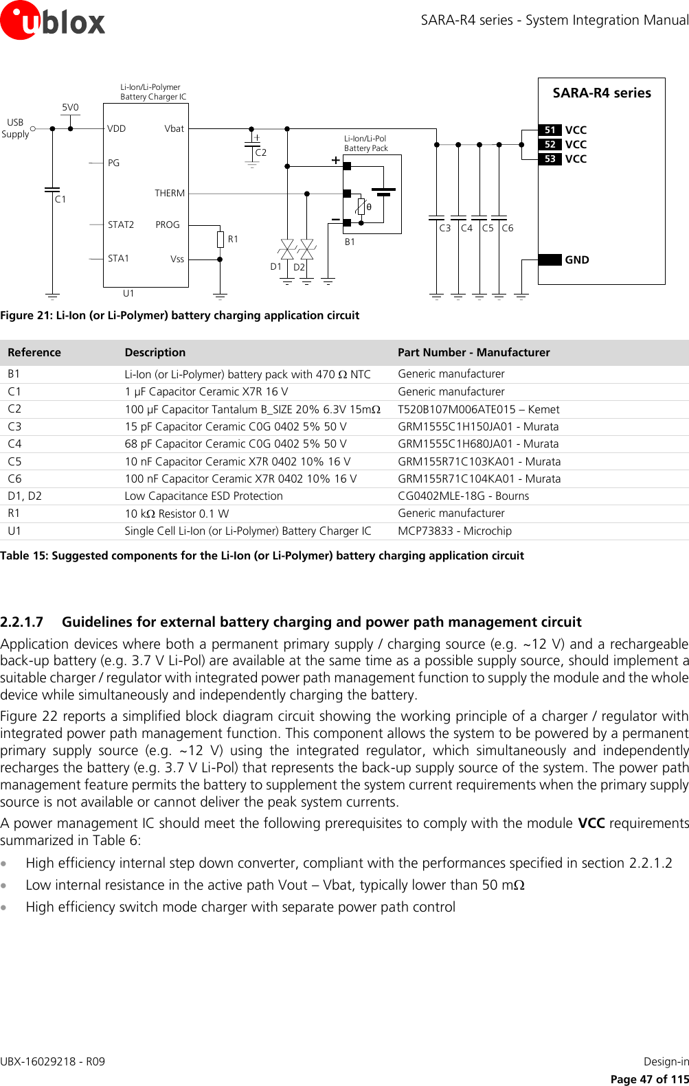
![SARA-R4 series - System Integration Manual UBX-16029218 - R09 Design-in Page 46 of 115 2.2.1.4 Guidelines for VCC supply circuit design using a rechargeable Li-Ion or Li-Pol battery Rechargeable Li-Ion or Li-Pol batteries connected to the VCC pins should meet the following prerequisites to comply with the module VCC requirements summarized in Table 6: Maximum pulse and DC discharge current: the rechargeable Li-Ion battery with its related output circuit connected to the VCC pins must be capable of delivering the maximum current occurring during a transmission at maximum Tx power, as specified in the SARA-R4 series Data Sheet [1]. The maximum discharge current is not always reported in the data sheets of batteries, but the maximum DC discharge current is typically almost equal to the battery capacity in Amp-hours divided by 1 hour. DC series resistance: the rechargeable Li-Ion battery with its output circuit must be capable of avoiding a VCC voltage drop below the operating range summarized in Table 6 during transmit bursts. 2.2.1.5 Guidelines for VCC supply circuit design using a primary (disposable) battery The characteristics of a primary (non-rechargeable) battery connected to VCC pins should meet the following prerequisites to comply with the module VCC requirements summarized in Table 6: Maximum pulse and DC discharge current: the non-rechargeable battery with its related output circuit connected to the VCC pins must be capable of delivering the maximum current consumption occurring during a transmission at maximum Tx power, as specified in the SARA-R4 series Data Sheet [1]. The maximum discharge current is not always reported in the data sheets of batteries, but the maximum DC discharge current is typically almost equal to the battery capacity in Amp-hours divided by 1 hour. DC series resistance: the non-rechargeable battery with its output circuit must be capable of avoiding a VCC voltage drop below the operating range summarized in Table 6 during transmit bursts. 2.2.1.6 Guidelines for external battery charging circuit SARA-R4 series modules do not have an on-board charging circuit. Figure 21 provides an example of a battery charger design, suitable for applications that are battery powered with a Li-Ion (or Li-Polymer) cell. In the application circuit, a rechargeable Li-Ion (or Li-Polymer) battery cell, that features the correct pulse and DC discharge current capabilities and the appropriate DC series resistance, is directly connected to the VCC supply input of the module. Battery charging is completely managed by the Battery Charger IC, which from a USB power source (5.0 V typ.), linearly charges the battery in three phases: Pre-charge constant current (active when the battery is deeply discharged): the battery is charged with a low current. Fast-charge constant current: the battery is charged with the maximum current, configured by the value of an external resistor. Constant voltage: when the battery voltage reaches the regulated output voltage, the Battery Charger IC starts to reduce the current until the charge termination is done. The charging process ends when the charging current reaches the value configured by an external resistor or when the charging timer reaches the factory set value. Using a battery pack with an internal NTC resistor, the Battery Charger IC can monitor the battery temperature to protect the battery from operating under unsafe thermal conditions. The Battery Charger IC, as linear charger, is more suitable for applications where the charging source has a relatively low nominal voltage (~5 V), so that a switching charger is suggested for applications where the charging source has a relatively high nominal voltage (e.g. ~12 V, see section 2.2.1.7 for the specific design-in).](https://usermanual.wiki/u-blox/2AGQN4NNN.User-Manual-2/User-Guide-3940431-Page-46.png)
![SARA-R4 series - System Integration Manual UBX-16029218 - R09 Design-in Page 51 of 115 2.2.1.9 Guidelines for removing VCC supply Removing the VCC power can be useful to minimize the current consumption when the SARA-R4 series modules are switched off or when the modules are in deep sleep Power Saving Mode. In applications in which the module is paired to a host application processor equipped with a RTC, the module can execute standard PSM procedures, store NAS protocol context in non-volatile memory, and rely on the host application processor to run its RTC and to trigger wake-up upon need. The application processor can disconnect the VCC supply source from the module and zero out the module’s PSM current. The VCC supply source can be removed using an appropriate low-leakage load switch or p-channel MOSFET controlled by the application processor as shown in Figure 25, given that the external switch has provide: Very low leakage current (for example, less than 1 µA), to minimize the current consumption Very low RDS(ON) series resistance (for example, less than 50 m), to minimize voltage drops Adequate maximum Drain current (see the SARA-R4 series Data Sheet [1] for module consumption figures) C3GNDC2C1 C4SARA-R4 series52 VCC53 VCC51 VCCVCC Supply SourceGNDC5U1VOUTVINVBIASONCTGND4V_INT15 PWR_ONR1R2T1GPIOApplication Processor GPIOGPIO+ Figure 25: Example of application circuit for VCC supply removal Reference Description Part Number - Manufacturer C1 100 µF Capacitor Tantalum B_SIZE 20% 6.3V 15m T520B107M006ATE015 – Kemet C2 10 nF Capacitor Ceramic X7R 0402 10% 16 V GRM155R71C103KA01 - Murata C3 100 nF Capacitor Ceramic X7R 0402 10% 16 V GRM155R61A104KA01 - Murata C4 68 pF Capacitor Ceramic C0G 0402 5% 50 V GRM1555C1H680JA01 - Murata C5 15 pF Capacitor Ceramic C0G 0402 5% 25 V GRM1555C1E150JA01 - Murata R1, R3 47 k Resistor 0402 5% 0.1 W RC0402JR-0747KL - Yageo Phycomp R2 10 k Resistor 0402 5% 0.1 W RC0402JR-0710KL - Yageo Phycomp T1 NPN BJT Transistor BC847 - Infineon U1 Ultra-Low Resistance Load Switch TPS22967 - Texas Instruments Table 18: Components for VCC supply removal application circuit It is highly recommended to avoid an abrupt removal of the VCC supply during SARA-R4 series normal operations: the VCC supply can be removed only after V_INT goes low, indicating that the module has entered Deep-Sleep Power Saving Mode or Power-Off Mode.](https://usermanual.wiki/u-blox/2AGQN4NNN.User-Manual-2/User-Guide-3940431-Page-51.png)
![SARA-R4 series - System Integration Manual UBX-16029218 - R09 Design-in Page 54 of 115 2.2.2 Generic digital interfaces supply output (V_INT) 2.2.2.1 Guidelines for V_INT circuit design SARA-R4 series provide the V_INT generic digital interfaces 1.8 V supply output, which can be mainly used to: Indicate when the module is switched on and it is not in the deep sleep power saving mode (as described in sections 1.6.1, 1.6.2) Pull-up SIM detection signal (see section 2.5 for more details) Supply voltage translators to connect 1.8 V module generic digital interfaces to 3.0 V devices (e.g. see 2.6.1) Enable external voltage regulators providing supply for external devices Do not apply loads which might exceed the limit for maximum available current from V_INT supply (see the SARA-R4 series Data Sheet [1]) as this can cause malfunctions in internal circuitry. V_INT can only be used as an output: do not connect any external supply source on V_INT. ESD sensitivity rating of the V_INT supply pin is 1 kV (Human Body Model according to JESD22-A114). Higher protection level could be required if the line is externally accessible and it can be achieved by mounting an ESD protection (e.g. EPCOS CA05P4S14THSG varistor array) close to the accessible point. It is recommended to monitor the V_INT pin to sense the end of the internal switch-off sequence of SARA-R4 series modules: VCC supply can be removed only after V_INT goes low. It is recommended to provide direct access to the V_INT pin on the application board by means of an accessible test point directly connected to the V_INT pin.](https://usermanual.wiki/u-blox/2AGQN4NNN.User-Manual-2/User-Guide-3940431-Page-54.png)
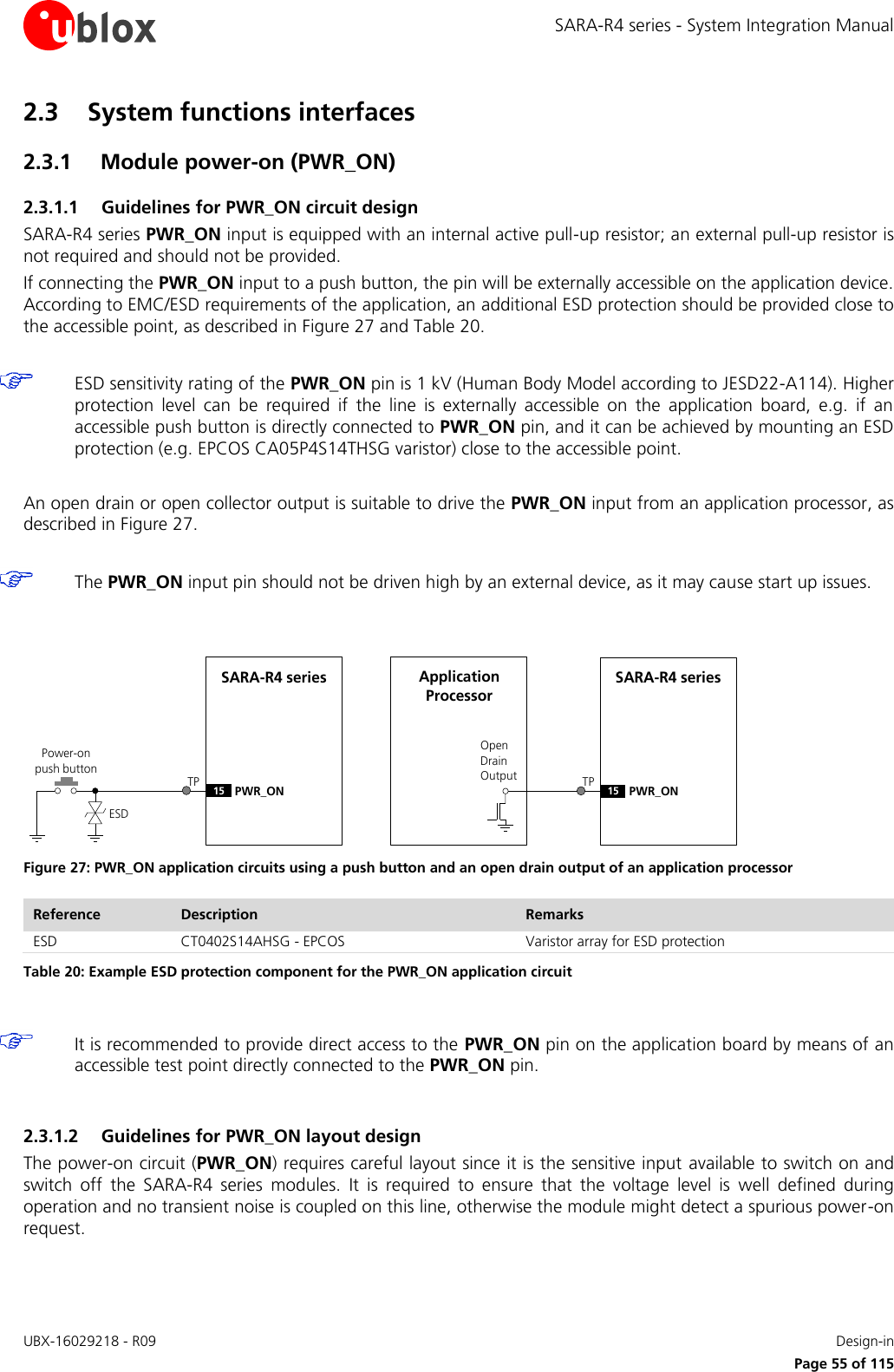
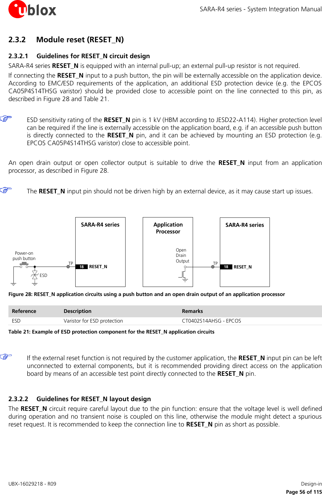
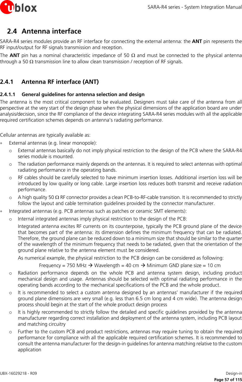
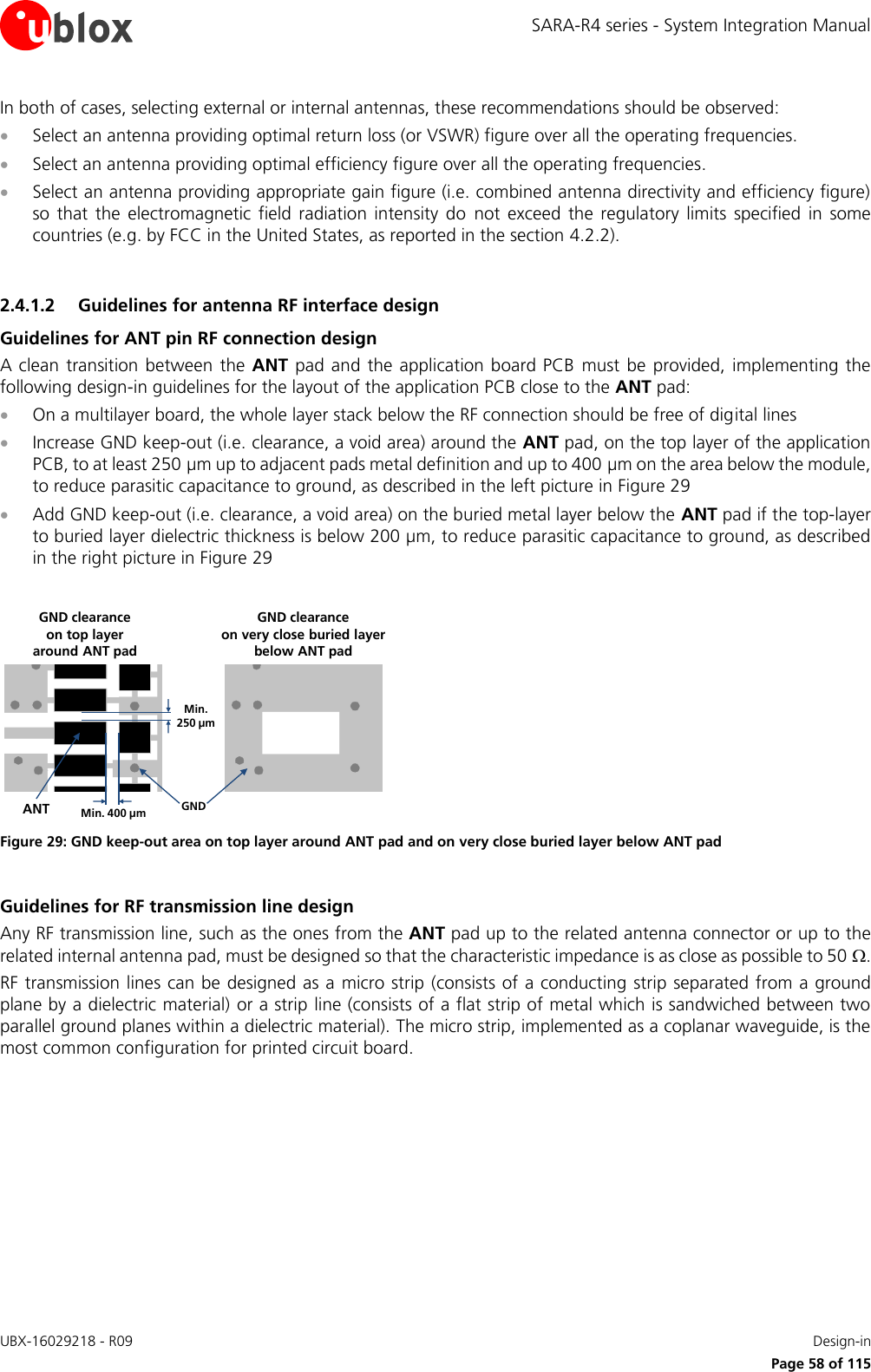
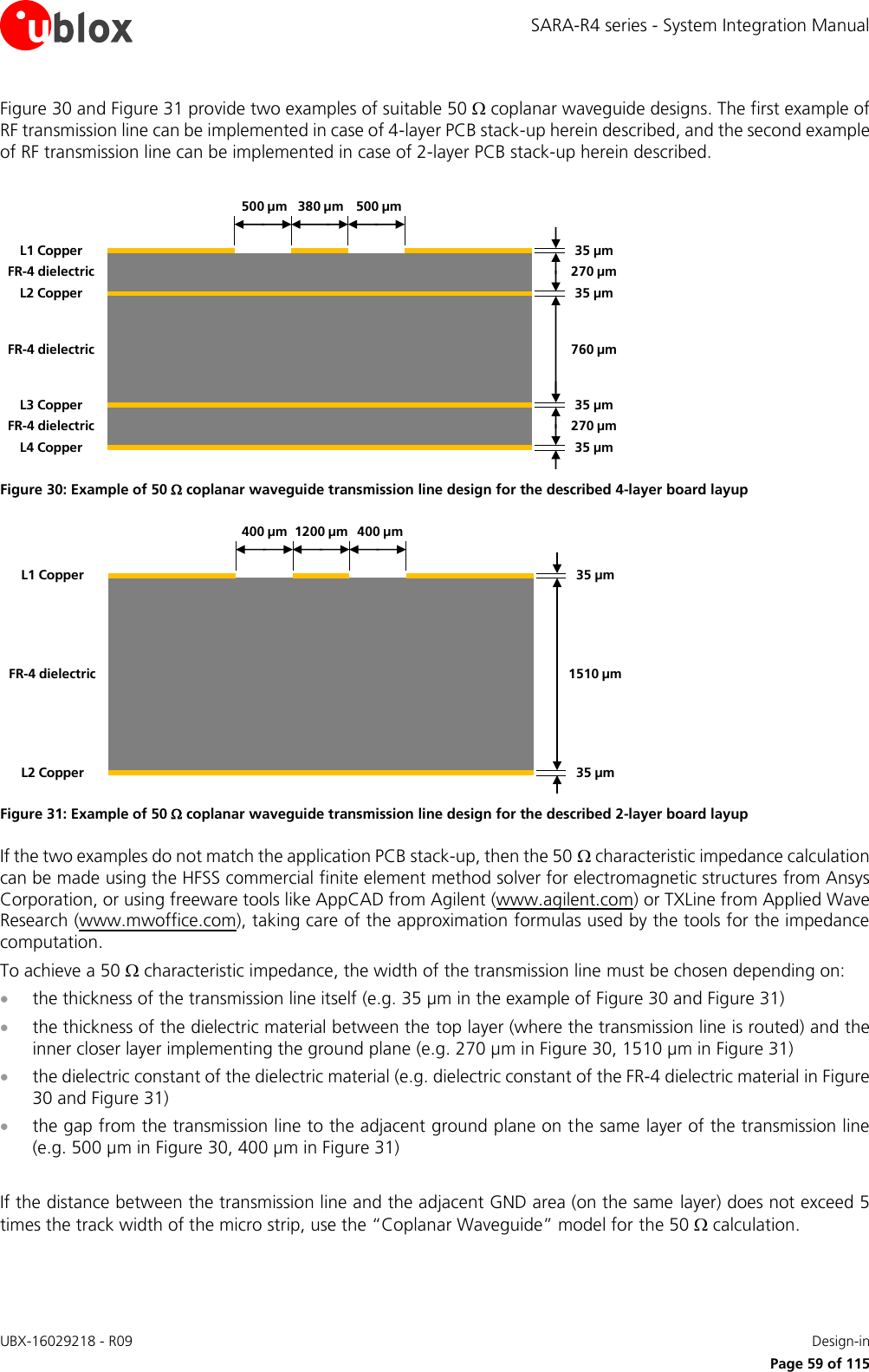
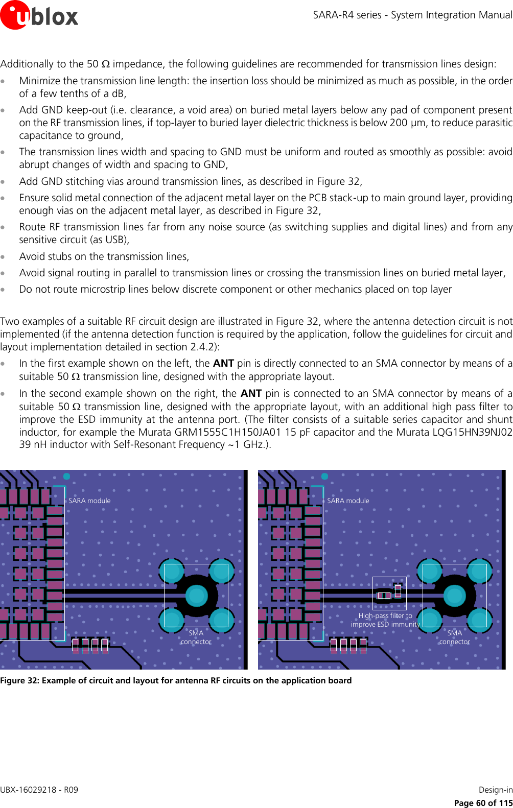
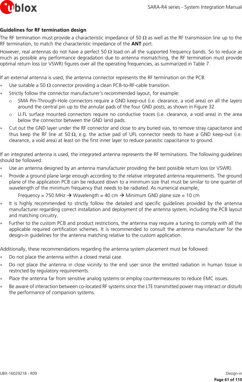
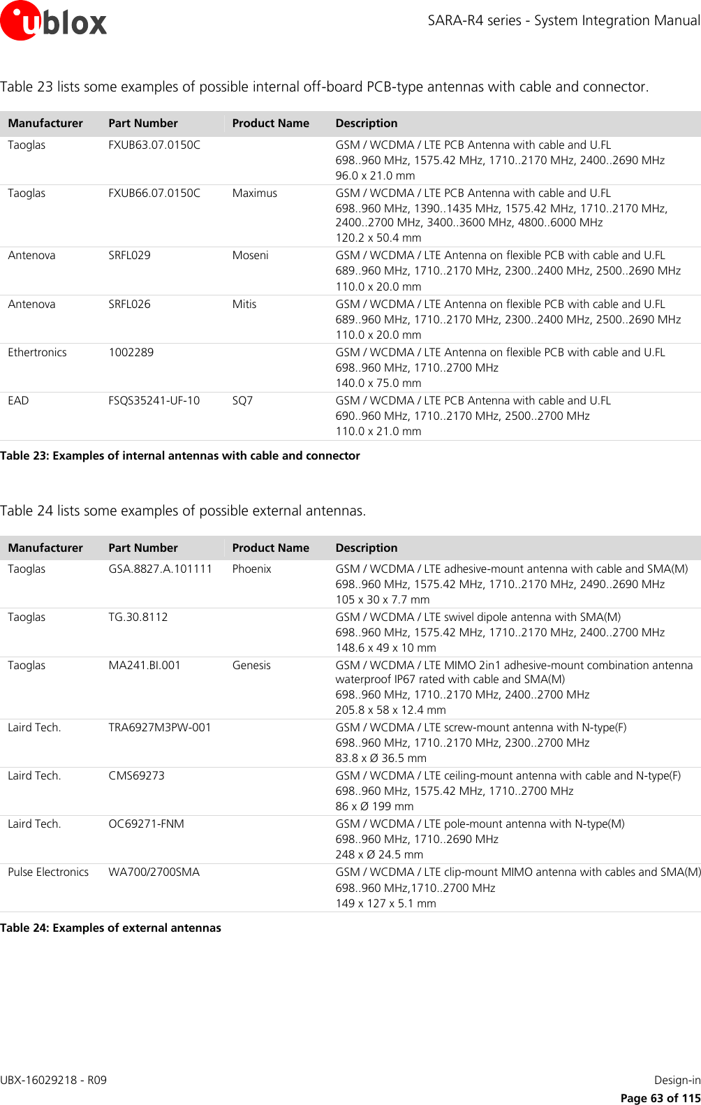
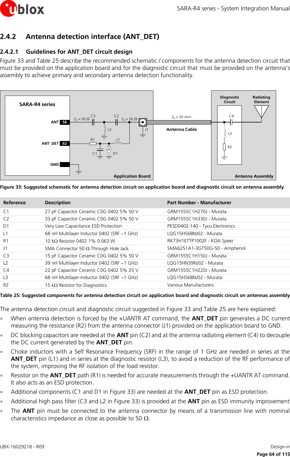
![SARA-R4 series - System Integration Manual UBX-16029218 - R09 Design-in Page 65 of 115 The DC impedance at RF port for some antennas may be a DC open (e.g. linear monopole) or a DC short to reference GND (e.g. PIFA antenna). For those antennas, without the diagnostic circuit of Figure 33, the measured DC resistance is always at the limits of the measurement range (respectively open or short), and there is no mean to distinguish between a defect on antenna path with similar characteristics (respectively: removal of linear antenna or RF cable shorted to GND for PIFA antenna). Furthermore, any other DC signal injected to the RF connection from ANT connector to radiating element will alter the measurement and produce invalid results for antenna detection. It is recommended to use an antenna with a built-in diagnostic resistor in the range from 5 k to 30 k to assure good antenna detection functionality and avoid a reduction of module RF performance. The choke inductor should exhibit a parallel Self Resonance Frequency (SRF) in the range of 1 GHz to improve the RF isolation of load resistor. For example: Consider an antenna with built-in DC load resistor of 15 k. Using the +UANTR AT command, the module reports the resistance value evaluated from the antenna connector provided on the application board to GND: Reported values close to the used diagnostic resistor nominal value (i.e. values from 13 k to 17 k if a 15 k diagnostic resistor is used) indicate that the antenna is correctly connected. Values close to the measurement range maximum limit (approximately 50 k) or an open-circuit “over range” report (see the SARA-R4 series AT Commands Manual [2]) means that that the antenna is not connected or the RF cable is broken. Reported values below the measurement range minimum limit (1 k) highlights a short to GND at antenna or along the RF cable. Measurement inside the valid measurement range and outside the expected range may indicate an unclean connection, a damaged antenna or incorrect value of the antenna load resistor for diagnostics. Reported value could differ from the real resistance value of the diagnostic resistor mounted inside the antenna assembly due to antenna cable length, antenna cable capacity and the used measurement method. If the antenna detection function is not required by the customer application, the ANT_DET pin can be left not connected and the ANT pin can be directly connected to the antenna connector by means of a 50 transmission line as described in Figure 32.](https://usermanual.wiki/u-blox/2AGQN4NNN.User-Manual-2/User-Guide-3940431-Page-65.png)
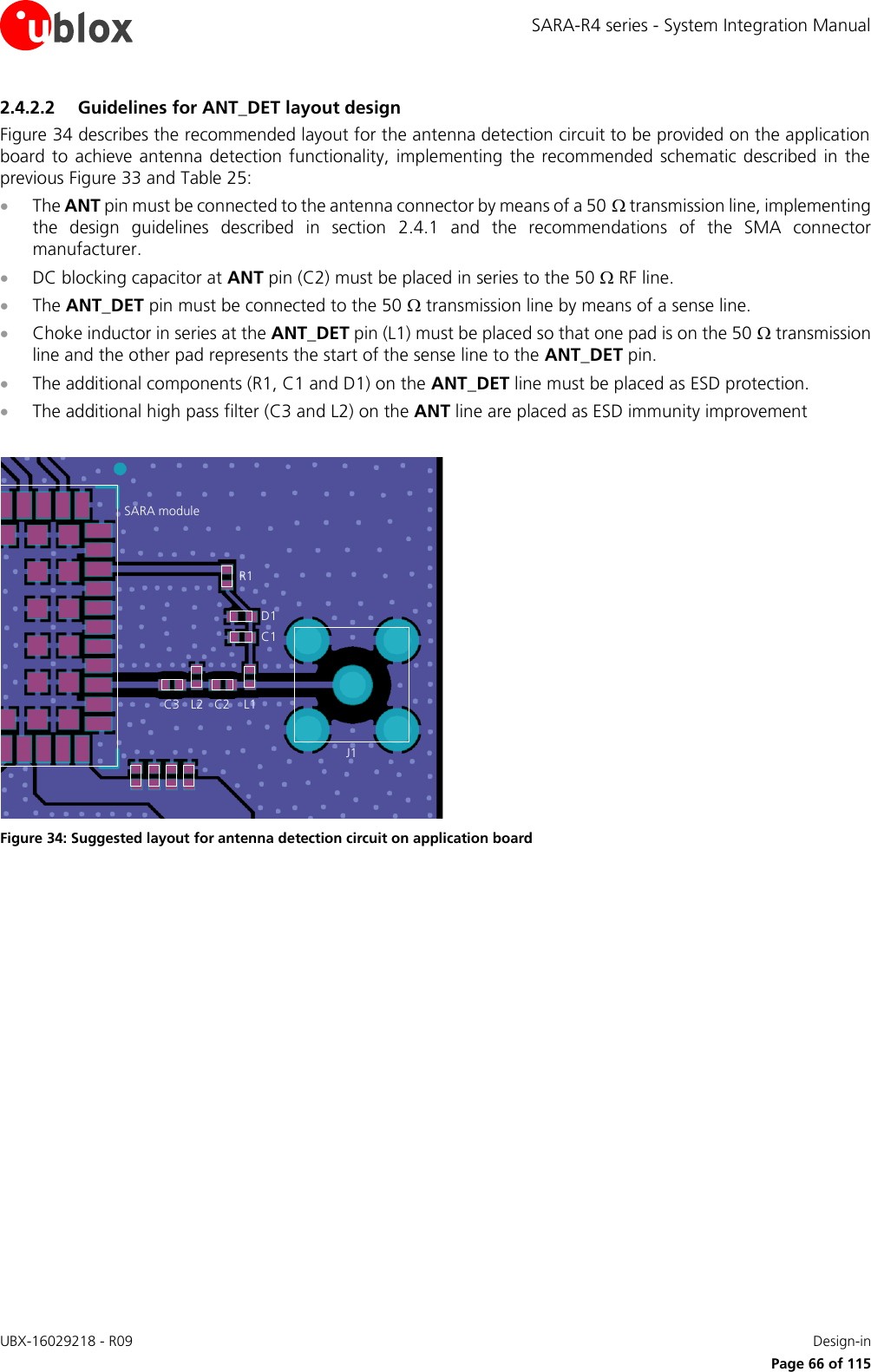
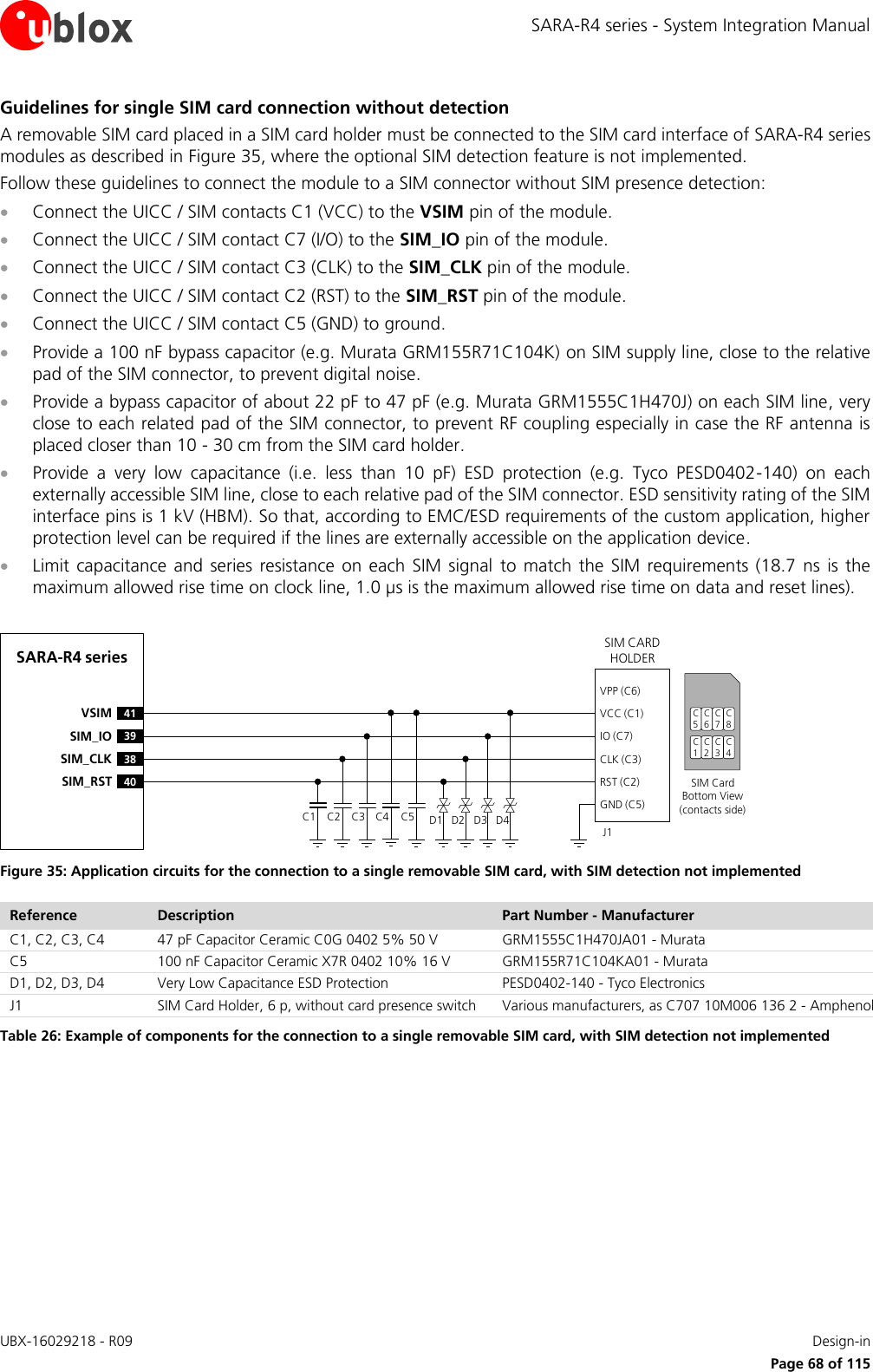
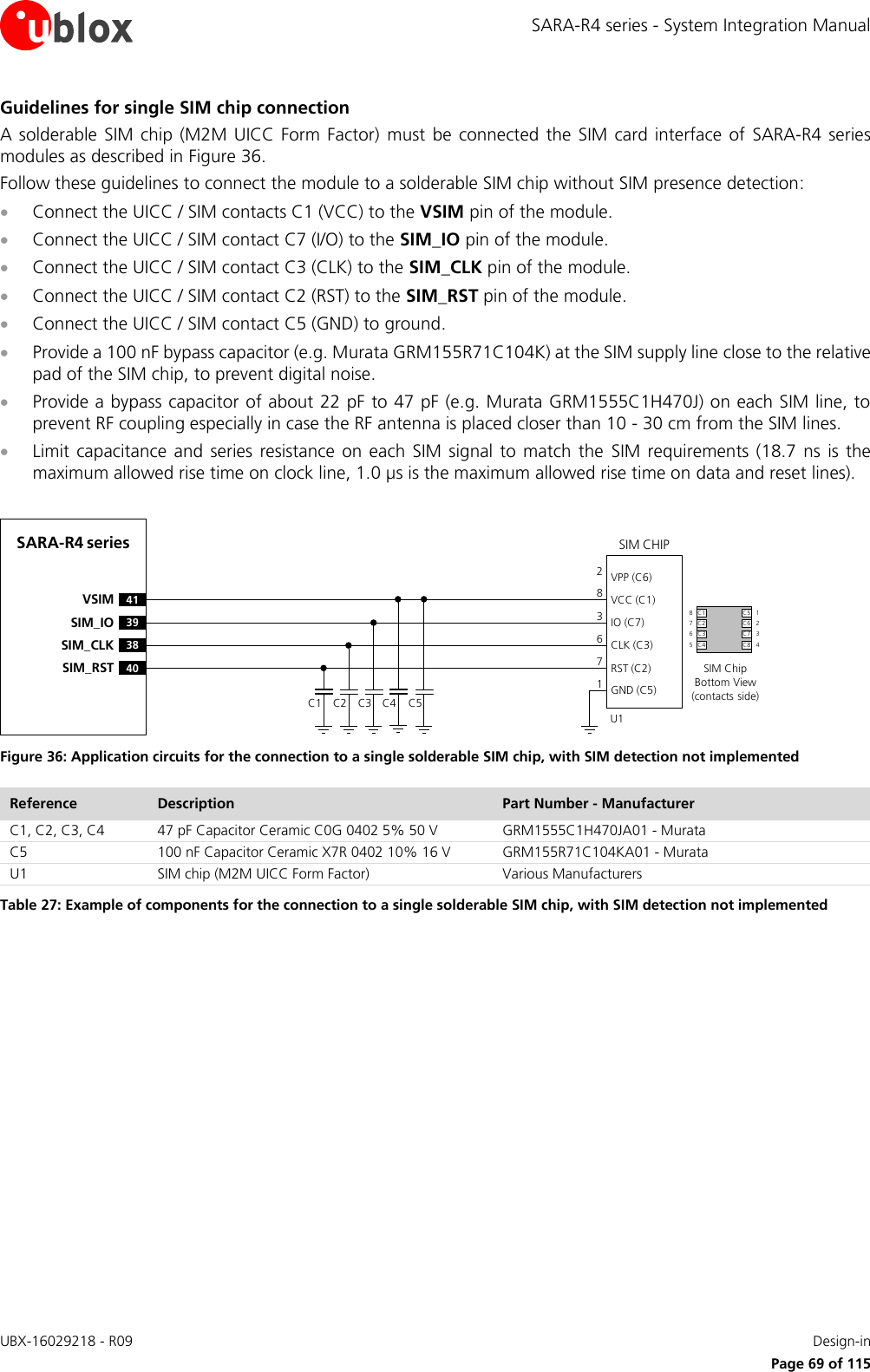
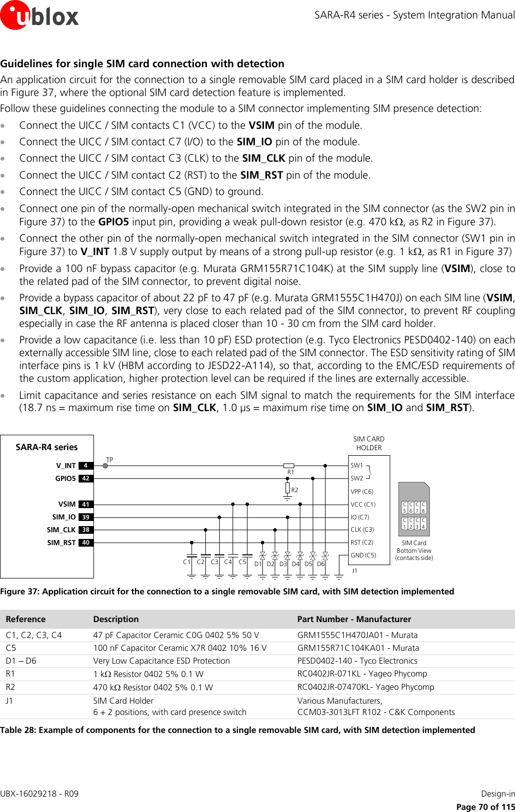
![SARA-R4 series - System Integration Manual UBX-16029218 - R09 Design-in Page 74 of 115 Providing the TXD, RXD, RTS and CTS lines only (not using the complete V.24 link)11 If the functionality of the DSR, DCD, RI and DTR lines is not required, or the lines are not available: Connect the module DTR input to GND using a 0 series resistor, since it may be useful to set DTR active if not specifically handled, in particular to have URCs presented over the UART interface (see the SARA-R4 series AT Commands Manual [1] for the &D, S0, +CNMI AT commands) Leave DSR, DCD and RI lines of the module floating, with a test-point on DCD If RS-232 compatible signal levels are needed, the Maxim MAX13234E voltage level translator can be used. This chip translates voltage levels from 1.8 V (module side) to the RS-232 standard. If a 1.8 V Application Processor is used, the circuit should be implemented as described in Figure 42. TxDApplication Processor(1.8V DTE)RxDRTSCTSDTRDSRRIDCDGNDSARA-R4(1.8V DCE)12 TXD9DTR13 RXD10 RTS11 CTS6DSR7RI8DCDGND0ΩTP0ΩTP0ΩTP0ΩTP Figure 42: UART interface application circuit with a partial V.24 link (5-wire) in the DTE/DCE serial communication (1.8V DTE) If a 3.0 V Application Processor (DTE) is used, then it is recommended to connect the 1.8 V UART interface of the module (DCE) by means of appropriate unidirectional voltage translators using the module V_INT output as 1.8 V supply for the voltage translators on the module side, as described in Figure 43. 4V_INTTxDApplication Processor(3.0V DTE)RxDRTSCTSDTRDSRRIDCDGNDSARA-R4 series (1.8V DCE)12 TXD9DTR13 RXD10 RTS11 CTS6DSR7RI8DCDGND1V8B1 A1GNDU1B3A3VCCBVCCAUnidirectionalVoltage TranslatorC1 C23V0DIR3DIR2 OEDIR1VCCB2 A2B4A4DIR4TP0ΩTP0ΩTP0ΩTPTP Figure 43: UART interface application circuit with a partial V.24 link (5-wire) in DTE/DCE serial communication (3.0 V DTE) Reference Description Part Number - Manufacturer C1, C2 100 nF Capacitor Ceramic X7R 0402 10% 16 V GRM155R61A104KA01 - Murata U1 Unidirectional Voltage Translator SN74AVC4T77412 - Texas Instruments Table 31: Component for UART application circuit with a partial V.24 link (5-wire) in DTE/DCE serial communication (3.0 V DTE) 11 Flow control is not supported by ‘00’, ‘01’ and SARA-R410M-02B product versions, but the RTS input must be set low to use the UART on ‘00’ and ‘01’ versions. The DTR input of the module must be set low to have URCs presented over UART on ‘00’, ‘01’ and ‘02’ product versions. 12 Voltage translator providing partial power down feature so that the DTE 3 V supply can be also ramped up before the V_INT 1.8 V supply](https://usermanual.wiki/u-blox/2AGQN4NNN.User-Manual-2/User-Guide-3940431-Page-74.png)
![SARA-R4 series - System Integration Manual UBX-16029218 - R09 Design-in Page 75 of 115 Providing the TXD and RXD lines only (not using the complete V24 link)13 If the functionality of the CTS, RTS, DSR, DCD, RI and DTR lines is not required in the application, or the lines are not available, then: Connect the module RTS input line to GND or to the CTS output line of the module, since the module requires RTS active (low electrical level) if HW flow-control is enabled (AT&K3, which is the default setting) Connect the module DTR input line to GND using a 0 series resistor, because it is useful to set DTR active if not specifically handled, in particular to have URCs presented over the UART interface (see the SARA-R4 series AT Commands Manual [1] for the &D, S0, +CNMI AT commands) Leave DSR, DCD and RI lines of the module floating, with a test-point on DCD If RS-232 compatible signal levels are needed, the Maxim MAX13234E voltage level translator can be used. This chip translates voltage levels from 1.8 V (module side) to the RS-232 standard. If a 1.8 V Application Processor (DTE) is used, the circuit that should be implemented as described in Figure 44 TxDApplication Processor(1.8V DTE)RxDRTSCTSDTRDSRRIDCDGNDSARA-R4(1.8V DCE)12 TXD9DTR13 RXD10 RTS11 CTS6DSR7RI8DCDGND0ΩTP0ΩTP0ΩTPTP Figure 44: UART interface application circuit with a partial V.24 link (3-wire) in the DTE/DCE serial communication (1.8V DTE) If a 3.0 V Application Processor (DTE) is used, then it is recommended to connect the 1.8 V UART interface of the module (DCE) by means of appropriate unidirectional voltage translators using the module V_INT output as 1.8 V supply for the voltage translators on the module side, as described in Figure 45. 4V_INTTxDApplication Processor(3.0V DTE)RxDDTRDSRRIDCDGNDSARA-R4(1.8V DCE)12 TXD9DTR13 RXD6DSR7RI8DCDGND1V8B1 A1GNDU1VCCBVCCAUnidirectionalVoltage TranslatorC1 C23V0DIR1DIR2 OEVCCB2 A2RTSCTS10 RTS11 CTSTP0ΩTP0ΩTP0ΩTPTP Figure 45: UART interface application circuit with a partial V.24 link (3-wire) in DTE/DCE serial communication (3.0 V DTE) Reference Description Part Number - Manufacturer C1, C2 100 nF Capacitor Ceramic X7R 0402 10% 16 V GRM155R61A104KA01 - Murata U1 Unidirectional Voltage Translator SN74AVC2T24514 - Texas Instruments Table 32: Component for UART application circuit with a partial V.24 link (3-wire) in DTE/DCE serial communication (3.0 V DTE) 13 Flow control is not supported by ‘00’, ‘01’ and SARA-R410M-02B product versions, but the RTS input must be set low to use the UART on ‘00’ and ‘01’ versions. The DTR input of the module must be set low to have URCs presented over UART on ‘00’, ‘01’ and ‘02’ product versions. 14 Voltage translator providing partial power down feature so that the DTE 3 V supply can be also ramped up before the V_INT 1.8 V supply](https://usermanual.wiki/u-blox/2AGQN4NNN.User-Manual-2/User-Guide-3940431-Page-75.png)
![SARA-R4 series - System Integration Manual UBX-16029218 - R09 Design-in Page 77 of 115 2.6.2 USB interface 2.6.2.1 Guidelines for USB circuit design The USB_D+ and USB_D- lines carry the USB serial data and signaling. The lines are used in single-ended mode for full speed signaling handshake, as well as in differential mode for high speed signaling and data transfer. USB pull-up or pull-down resistors and external series resistors on USB_D+ and USB_D- lines as required by the USB 2.0 specification [4] are part of the module USB pins driver and do not need to be externally provided. The USB interface of the module is enabled only if a valid voltage is detected by the VUSB_DET input (see the SARA-R4 series Data Sheet [1]). Neither the USB interface nor the whole module is supplied by the VUSB_DET input: the VUSB_DET senses the USB supply voltage and absorbs few microamperes. Routing the USB pins to a connector, they will be externally accessible on the application device. According to EMC/ESD requirements of the application, an additional ESD protection device with very low capacitance should be provided close to accessible point on the line connected to this pin, as described in Figure 46 and Table 33. The USB interface pins ESD sensitivity rating is 1 kV (Human Body Model according to JESD22-A114F). Higher protection level could be required if the lines are externally accessible and it can be achieved by mounting a very low capacitance (i.e. less or equal to 1 pF) ESD protection (e.g. Tyco Electronics PESD0402-140 ESD protection device) on the lines connected to these pins, close to accessible points. The USB pins of the modules can be directly connected to the USB host application processor without additional ESD protections if they are not externally accessible or according to EMC/ESD requirements. D+D-GND29 USB_D+28 USB_D-GNDUSB DEVICE CONNECTORVBUSD+D-GND29 USB_D+28 USB_D-GNDUSB HOST PROCESSORSARA-R4 series SARA-R4 series VBUS 17 VUSB_DET17 VUSB_DETD1 D2 D3 C1 C10ΩTest-Point0ΩTest-Point0ΩTest-Point Figure 46: USB Interface application circuits Reference Description Part Number - Manufacturer C1 100 nF Capacitor Ceramic X7R 0402 10% 16 V GRM155R61A104KA01 - Murata D1, D2, D3 Very Low Capacitance ESD Protection PESD0402-140 - Tyco Electronics Table 33: Components for USB application circuits If the USB interface is enabled, the module does not enter the low power deep sleep mode: the external USB VBUS supply voltage needs to be removed from the VUSB_DET input of the module to let it enter the Power Saving Mode defined in 3GPP Rel.13. If the USB interface pins are not used, they can be left unconnected on the application board, but it is strongly recommended to provide accessible test points directly connected to the USB interface pins (VUSB_DET, USB_D+, USB_D-).](https://usermanual.wiki/u-blox/2AGQN4NNN.User-Manual-2/User-Guide-3940431-Page-77.png)
![SARA-R4 series - System Integration Manual UBX-16029218 - R09 Design-in Page 78 of 115 2.6.2.2 Guidelines for USB layout design The USB_D+ / USB_D- lines require accurate layout design to achieve reliable signaling at the high speed data rate (up to 480 Mb/s) supported by the USB serial interface. The characteristic impedance of the USB_D+ / USB_D- lines is specified by the Universal Serial Bus Revision 2.0 specification [4]. The most important parameter is the differential characteristic impedance applicable for the odd-mode electromagnetic field, which should be as close as possible to 90 differential. Signal integrity may be degraded if PCB layout is not optimal, especially when the USB signaling lines are very long. Use the following general routing guidelines to minimize signal quality problems: Route USB_D+ / USB_D- lines as a differential pair Route USB_D+ / USB_D- lines as short as possible Ensure the differential characteristic impedance (Z0) is as close as possible to 90 Ensure the common mode characteristic impedance (ZCM) is as close as possible to 30 Consider design rules for USB_D+ / USB_D- similar to RF transmission lines, being them coupled differential micro-strip or buried stripline: avoid any stubs, abrupt change of layout, and route on clear PCB area Figure 47 and Figure 48 provide two examples of coplanar waveguide designs with differential characteristic impedance close to 90 and common mode characteristic impedance close to 30 . The first transmission line can be implemented in case of 4-layer PCB stack-up herein described, the second transmission line can be implemented in case of 2-layer PCB stack-up herein described. 35 µm35 µm35 µm35 µm270 µm270 µm760 µmL1 CopperL3 CopperL2 CopperL4 CopperFR-4 dielectricFR-4 dielectricFR-4 dielectric350 µm 400 µm400 µm350 µm400 µm Figure 47: Example of USB line design, with Z0 close to 90 and ZCM close to 30 , for the described 4-layer board layup 35 µm35 µm1510 µmL2 CopperL1 CopperFR-4 dielectric740 µm 410 µm410 µm740 µm410 µm Figure 48: Example of USB line design, with Z0 close to 90 and ZCM close to 30 , for the described 2-layer board layup](https://usermanual.wiki/u-blox/2AGQN4NNN.User-Manual-2/User-Guide-3940431-Page-78.png)
![SARA-R4 series - System Integration Manual UBX-16029218 - R09 Design-in Page 79 of 115 2.6.3 SPI interface 2.6.3.1 Guidelines for SPI circuit design The SPI interface is not supported by “00”, “01” and “02” product versions: the SPI interface pins should not be driven by any external device. 2.6.4 SDIO interface 2.6.4.1 Guidelines for SDIO circuit design The SDIO interface is not supported by “00”, “01” and “02” product versions: the SDIO interface pins should not be driven by any external device. 2.6.5 DDC (I2C) interface 2.6.5.1 Guidelines for DDC (I2C) circuit design DDC (I2C) interface is not supported by “00” and “01” product versions: the DDC (I2C) interface pins should not be driven by any external device. The DDC I2C-bus master interface can be used to communicate with u-blox GNSS receivers and other external I2C-bus slaves as an audio codec. The SDA and SCL pins of the module are open drain output as per I2C bus specifications [9], and they have internal pull-up resistors to the V_INT 1.8 V supply rail of the module, so there is no need of additional pull-up resistors on the external application board. Capacitance and series resistance must be limited on the bus to match the I2C specifications (1.0 µs is the maximum allowed rise time on the SCL and SDA lines): route connections as short as possible. ESD sensitivity rating of the DDC (I2C) pins is 1 kV (Human Body Model according to JESD22-A114). Higher protection level could be required if the lines are externally accessible and it can be achieved by mounting an ESD protection (e.g. EPCOS CA05P4S14THSG varistor array) close to accessible points. If the pins are not used as DDC bus interface, they can be left unconnected.](https://usermanual.wiki/u-blox/2AGQN4NNN.User-Manual-2/User-Guide-3940431-Page-79.png)
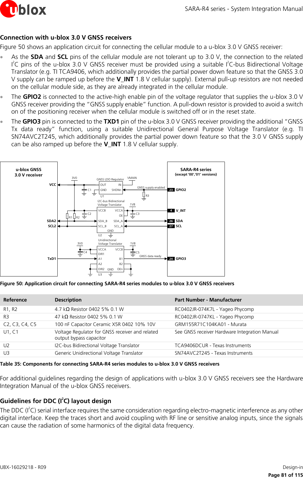
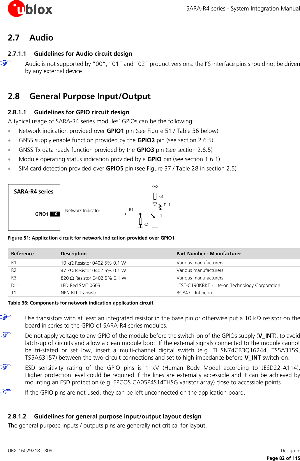
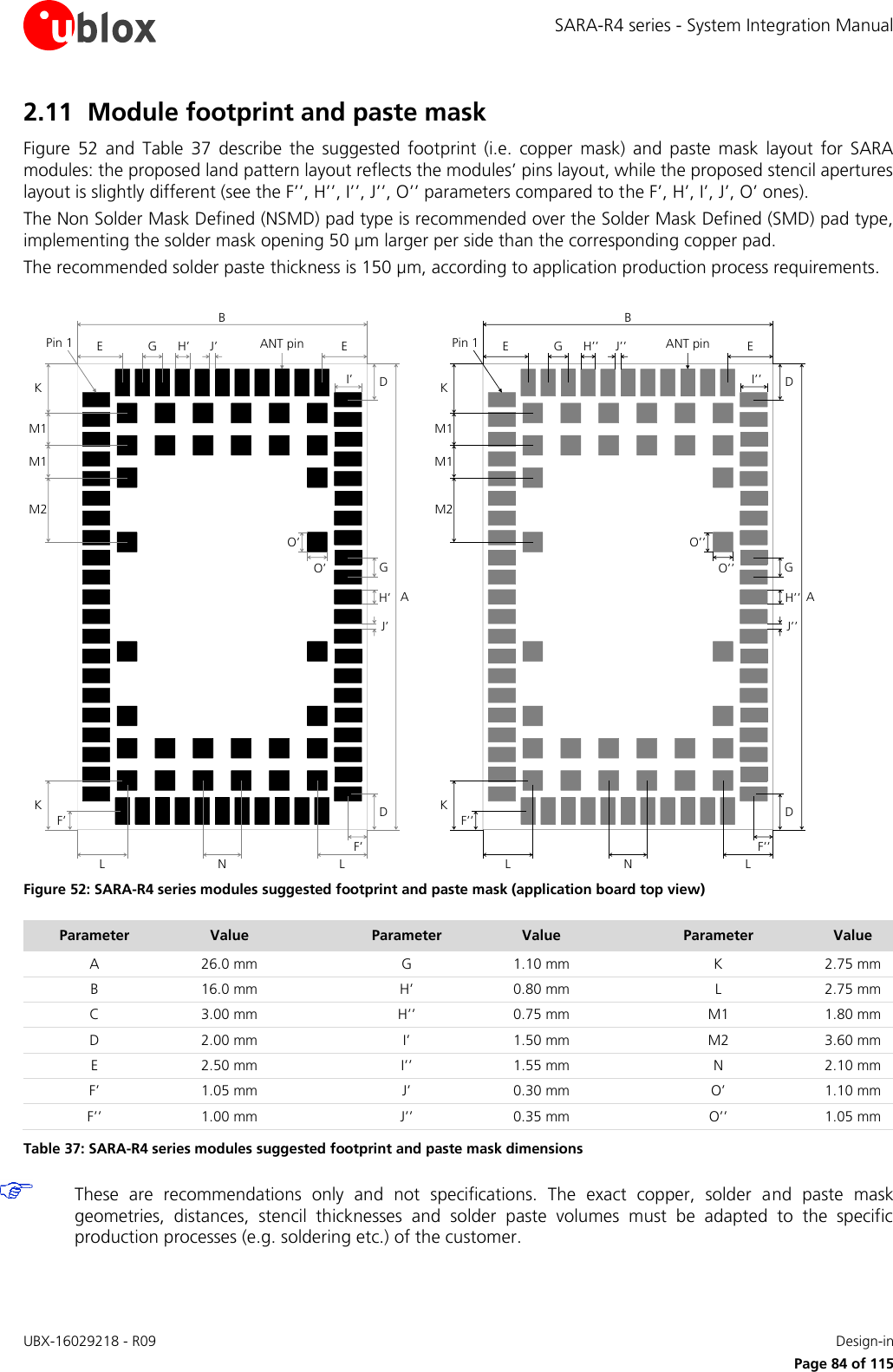
![SARA-R4 series - System Integration Manual UBX-16029218 - R09 Design-in Page 85 of 115 2.12 Thermal guidelines The module operating temperature range is specified in the SARA-R4 series Data Sheet [1]. The most critical condition concerning module thermal performance is the uplink transmission at maximum power (data upload in connected mode), when the baseband processor runs at full speed, radio circuits are all active and the RF power amplifier is driven to higher output RF power. This scenario is not often encountered in real networks (for example, see the Terminal Tx Power distribution for WCDMA, taken from operation on a live network, described in the GSMA TS.09 Battery Life Measurement and Current Consumption Technique [10]); however the application should be correctly designed to cope with it. During transmission at maximum RF power the SARA-R4 series modules generate thermal power that may exceed 0.5 W: this is an indicative value since the exact generated power strictly depends on operating condition such as the actual antenna return loss, the transmitting frequency band, etc. The generated thermal power must be adequately dissipated through the thermal and mechanical design of the application. The spreading of the Module-to-Ambient thermal resistance (Rth,M-A) depends on the module operating condition. The overall temperature distribution is influenced by the configuration of the active components during the specific mode of operation and their different thermal resistance toward the case interface. The Module-to-Ambient thermal resistance value and the relative increase of module temperature will differ according to the specific mechanical deployments of the module, e.g. application PCB with different dimensions and characteristics, mechanical shells enclosure, or forced air flow. The increase of the thermal dissipation, i.e. the reduction of the Module-to-Ambient thermal resistance, will decrease the temperature of the modules’ internal circuitry for a given operating ambient temperature. This improves the device long-term reliability in particular for applications operating at high ambient temperature. Recommended hardware techniques to be used to improve heat dissipation in the application: Connect each GND pin with solid ground layer of the application board and connect each ground area of the multilayer application board with complete thermal via stacked down to main ground layer. Provide a ground plane as wide as possible on the application board. Optimize antenna return loss, to optimize overall electrical performance of the module including a decrease of module thermal power. Optimize the thermal design of any high-power components included in the application, such as linear regulators and amplifiers, to optimize overall temperature distribution in the application device. Select the material, the thickness and the surface of the box (i.e. the mechanical enclosure) of the application device that integrates the module so that it provides good thermal dissipation. Beside the reduction of the Module-to-Ambient thermal resistance implemented by correct application hardware design, the increase of module temperature can be moderated by a correspondingly correct application software implementation: Enable power saving configuration using the AT+CPSMS command Enable module connected mode for a given time period and then disable it for a time period long enough to adequately mitigate the temperature increase.](https://usermanual.wiki/u-blox/2AGQN4NNN.User-Manual-2/User-Guide-3940431-Page-85.png)
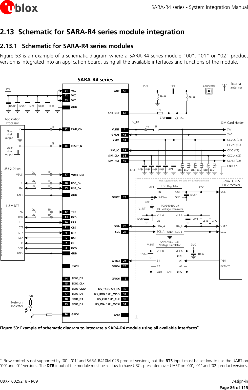
![SARA-R4 series - System Integration Manual UBX-16029218 - R09 Design-in Page 87 of 115 2.14 Design-in checklist This section provides a design-in checklist. 2.14.1 Schematic checklist The following are the most important points for a simple schematic check: DC supply must provide a nominal voltage at VCC pin within the operating range limits. DC supply must be capable of supporting the highest peak / pulse current consumption values and the maximum averaged current consumption values in connected mode, as specified in the SARA-R4 series Data Sheet [1]. VCC voltage supply should be clean, with very low ripple/noise: provide the suggested bypass capacitors, in particular if the application device integrates an internal antenna. Do not apply loads which might exceed the limit for maximum available current from V_INT supply. Check that voltage level of any connected pin does not exceed the relative operating range. Provide accessible test points directly connected to the following pins of the SARA-R4 series modules: V_INT, PWR_ON and RESET_N for diagnostic purposes. Capacitance and series resistance must be limited on each SIM signal to match the SIM specifications. Insert the suggested pF capacitors on each SIM signal and low capacitance ESD protections if accessible. Check UART signals direction, as the modules’ signal names follow the ITU-T V.24 Recommendation [5]. Capacitance and series resistance must be limited on each high speed line of the USB interface. It is strongly recommended to provide accessible test points directly connected to the USB interface pins (VUSB_DET, USB_D+ and USB_D- pins). Use transistors with at least an integrated resistor in the base pin or otherwise put a 10 k resistor on the board in series to the GPIO when those are used to drive LEDs. Provide adequate precautions for EMC / ESD immunity as required on the application board. Do not apply voltage to any generic digital interface pin of SARA-R4 series modules before the switch-on of the generic digital interface supply source (V_INT). All unused pins can be left unconnected.](https://usermanual.wiki/u-blox/2AGQN4NNN.User-Manual-2/User-Guide-3940431-Page-87.png)
![SARA-R4 series - System Integration Manual UBX-16029218 - R09 Handling and soldering Page 89 of 115 3 Handling and soldering No natural rubbers, no hygroscopic materials or materials containing asbestos are employed. 3.1 Packaging, shipping, storage and moisture preconditioning For information pertaining to SARA-R4 series reels / tapes, Moisture Sensitivity levels (MSD), shipment and storage information, as well as drying for preconditioning, see the SARA-R4 series Data Sheet [1] and the u-blox Package Information Guide [15]. 3.2 Handling The SARA-R4 series modules are Electro-Static Discharge (ESD) sensitive devices. Ensure ESD precautions are implemented during handling of the module. Electrostatic discharge (ESD) is the sudden and momentary electric current that flows between two objects at different electrical potentials caused by direct contact or induced by an electrostatic field. The term is usually used in the electronics and other industries to describe momentary unwanted currents that may cause damage to electronic equipment. The ESD sensitivity for each pin of SARA-R4 series modules (as Human Body Model according to JESD22-A114F) is specified in the SARA-R4 series Data Sheet [1]. ESD prevention is based on establishing an Electrostatic Protective Area (EPA). The EPA can be a small working station or a large manufacturing area. The main principle of an EPA is that there are no highly charging materials near ESD sensitive electronics, all conductive materials are grounded, workers are grounded, and charge build-up on ESD sensitive electronics is prevented. International standards are used to define typical EPA and can be obtained for example from the International Electrotechnical Commission (IEC) or the American National Standards Institute (ANSI). In addition to standard ESD safety practices, the following measures should be taken into account whenever handling the SARA-R4 series modules: Unless there is a galvanic coupling between the local GND (i.e. the work table) and the PCB GND, then the first point of contact when handling the PCB must always be between the local GND and PCB GND. Before mounting an antenna patch, connect the ground of the device. When handling the module, do not come into contact with any charged capacitors and be careful when contacting materials that can develop charges (e.g. patch antenna, coax cable, soldering iron). To prevent electrostatic discharge through the RF pin, do not touch any exposed antenna area. If there is any risk that such exposed antenna area is touched in a non-ESD protected work area, implement adequate ESD protection measures in the design. When soldering the module and patch antennas to the RF pin, make sure to use an ESD-safe soldering iron.](https://usermanual.wiki/u-blox/2AGQN4NNN.User-Manual-2/User-Guide-3940431-Page-89.png)
![SARA-R4 series - System Integration Manual UBX-16029218 - R09 Handling and soldering Page 91 of 115 The soldering temperature profile chosen at the factory depends on additional external factors like choice of soldering paste, size, thickness and properties of the base board, etc. Exceeding the maximum soldering temperature and the maximum liquidus time limit in the recommended soldering profile may permanently damage the module. Preheat Heating Cooling[°C] Peak Temp. 245°C [°C]250 250Liquidus Temperature217 217200 20040 - 60 sEnd Temp.max 4°C/s150 - 200°C150 150max 3°C/s60 - 120 s100 Typical Leadfree 100Soldering Profile50 50Elapsed time [s] Figure 54: Recommended soldering profile The modules must not be soldered with a damp heat process. 3.3.3 Optical inspection After soldering the module, inspect it optically to verify that the module is correctly aligned and centered. 3.3.4 Cleaning Cleaning the modules is not recommended. Residues underneath the modules cannot be easily removed with a washing process. Cleaning with water will lead to capillary effects where water is absorbed in the gap between the baseboard and the module. The combination of residues of soldering flux and encapsulated water leads to short circuits or resistor-like interconnections between neighboring pads. Water will also damage the sticker and the ink-jet printed text. Cleaning with alcohol or other organic solvents can result in soldering flux residues flooding into the two housings, areas that are not accessible for post-wash inspections. The solvent will also damage the sticker and the ink-jet printed text. Ultrasonic cleaning will permanently damage the module, in particular the quartz oscillators. For best results, use a "no clean" soldering paste and eliminate the cleaning step after the soldering. 3.3.5 Repeated reflow soldering Repeated reflow soldering processes and soldering the module upside-down are not recommended. Boards with components on both sides may require two reflow cycles. In this case, the module should always be placed on the side of the board that is submitted into the last reflow cycle. The reason for this (besides others) is the risk of the module falling off due to the significantly higher weight in relation to other components. u-blox gives no warranty against damages to the SARA-R4 series modules caused by performing more than a total of two reflow soldering processes (one reflow soldering process to mount the SARA-R4 series module, plus one reflow soldering process to mount other parts).](https://usermanual.wiki/u-blox/2AGQN4NNN.User-Manual-2/User-Guide-3940431-Page-91.png)
![SARA-R4 series - System Integration Manual UBX-16029218 - R09 Approvals Page 94 of 115 The manufacturer of the end-device that integrates a SARA-R4 series module has to take care of all the certification schemes approvals required by the specific integrating device to be deployed in the market. The required certification scheme approvals and relative testing specifications applicable to the end-device that integrates a SARA-R4 series module differ depending on the country or the region where the integrating device is intended to be deployed, on the relative vertical market of the device, on type, features and functionalities of the whole application device, and on the network operators where the device is intended to operate. It has to be noted that the “02” product versions onwards of SARA-R4 series modules include the capability to configure the device selecting the operating Mobile Network Operator Profile, Radio Access Technology, and Band: see SARA-R4 series AT Commands Manual [2], +UMNOPROF, +URAT, and +UBANDMASK AT commands. As these configuration decisions are made, u-blox reminds manufacturers of the end-device integrating the “02” product versions onwards of SARA-R4 series modules to take care of compliance with all the certification approvals requirements applicable to the specific integrating device to be deployed in the market. Check the appropriate applicability of the SARA-R4 series module’s approvals while starting the certification process of the device integrating the module: the re-use of the u-blox cellular module’s approval can significantly reduce the cost and time to market of the application device certification. The certification of the application device that integrates a SARA-R4 series module and the compliance of the application device with all the applicable certification schemes, directives and standards are the sole responsibility of the application device manufacturer. SARA-R4 series modules are certified according to all capabilities and options stated in the Protocol Implementation Conformance Statement document (PICS) of the module. The PICS, according to the 3GPP TS 36.521-2 [12] and 3GPP TS 36.523-2 [13], is a statement of the implemented and supported capabilities and options of a device. The PICS document of the application device integrating SARA-R4 series modules must be updated from the module PICS statement if any feature stated as supported by the module in its PICS document is not implemented or disabled in the application device. For more details regarding the AT commands settings that affect the PICS, see the SARA-R4 series AT Commands Manual [1]. Check the specific settings required for mobile network operators approvals as they may differ from the AT commands settings defined in the module as integrated in the application device.](https://usermanual.wiki/u-blox/2AGQN4NNN.User-Manual-2/User-Guide-3940431-Page-94.png)
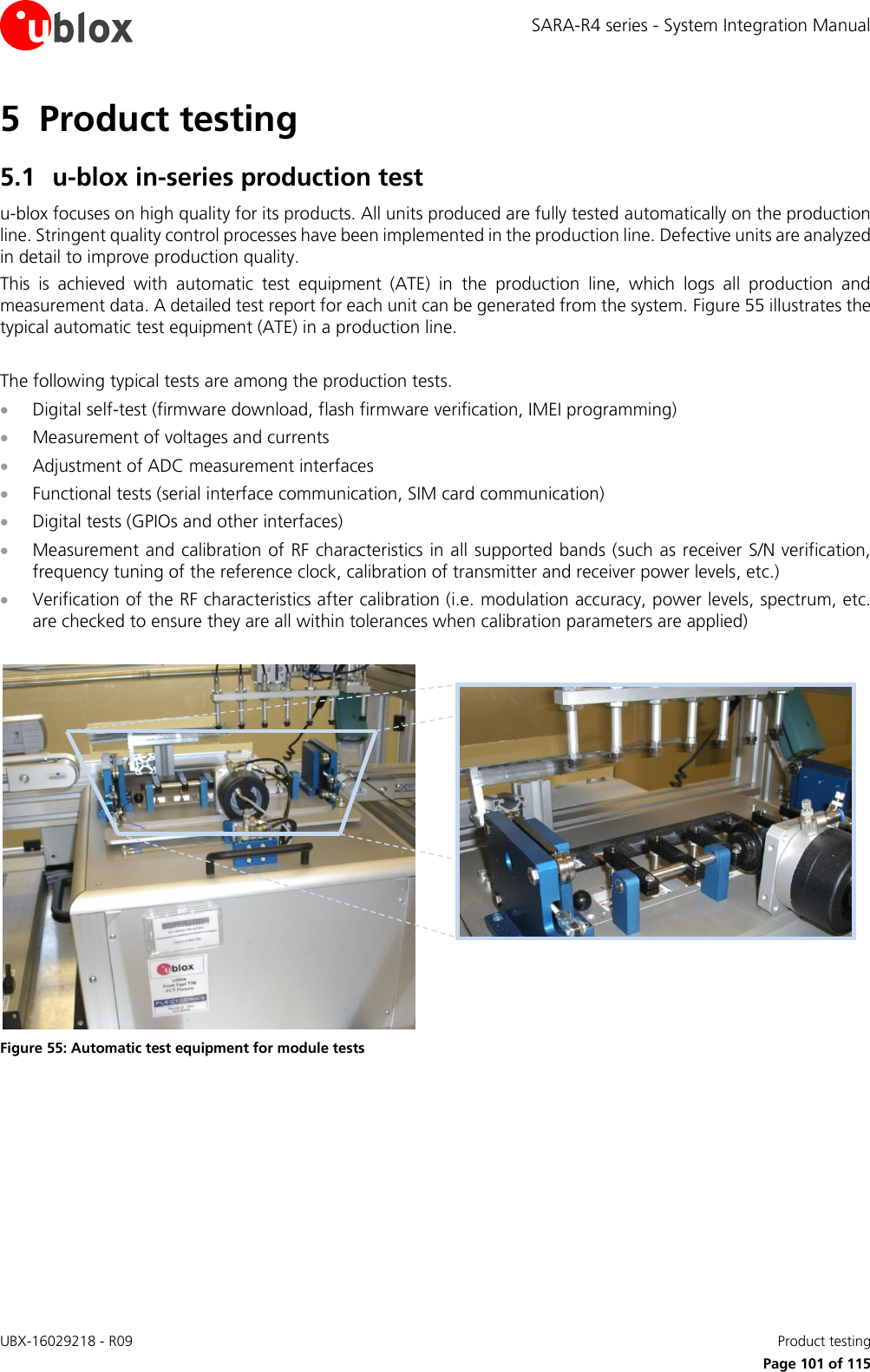
![SARA-R4 series - System Integration Manual UBX-16029218 - R09 Product testing Page 102 of 115 5.2 Test parameters for OEM manufacturers Because of the testing done by u-blox (with 100% coverage), an OEM manufacturer does not need to repeat the firmware tests or measurements of the module RF performance or tests over analog and digital interfaces in their production test. However, an OEM manufacturer should focus on: Module assembly on the device; it should be verified that: o The soldering and handling process did not damage the module components o All module pins are well soldered on the device board o There are no short circuits between pins Component assembly on the device; it should be verified that: o Communication with the host controller can be established o The interfaces between the module and device are working o Overall RF performance test of the device including the antenna Dedicated tests can be implemented to check the device. For example, the measurement of the module current consumption when set in a specified status can detect a short circuit if compared with a “Golden Device” result. In addition, module AT commands can be used to perform functional tests on the digital interfaces (communication with the host controller, check the SIM interface, GPIOs, etc.) or to perform RF performance tests (see the following section 5.2.2 for details). 5.2.1 “Go/No go” tests for integrated devices A “Go/No go” test is typically used to compare the signal quality with a “Golden Device” in a location with excellent network coverage and known signal quality. This test should be performed after the data connection has been established. These kinds of test may be useful as a “go/no go” test but not for RF performance measurements. This test is suitable to check the functionality of communications with the host controller, the SIM card and the power supply. It is also a means to verify if components at the antenna interface are well-soldered. 5.2.2 RF functional tests The overall RF functional test of the device including the antenna can be performed with basic instruments such as a spectrum analyzer (or an RF power meter) and a signal generator with the assistance of the AT+UTEST command over the AT command user interface. The AT+UTEST command provides a simple interface to set the module to Rx or Tx test modes ignoring the LTE signaling protocol. The command can set the module into: transmitting mode in a specified channel and power level in all supported bands receiving mode in a specified channel to return the measured power level in all supported bands See the SARA-R4 series AT Commands Manual [2] for the AT+UTEST command syntax description and detail guide of usage.](https://usermanual.wiki/u-blox/2AGQN4NNN.User-Manual-2/User-Guide-3940431-Page-102.png)
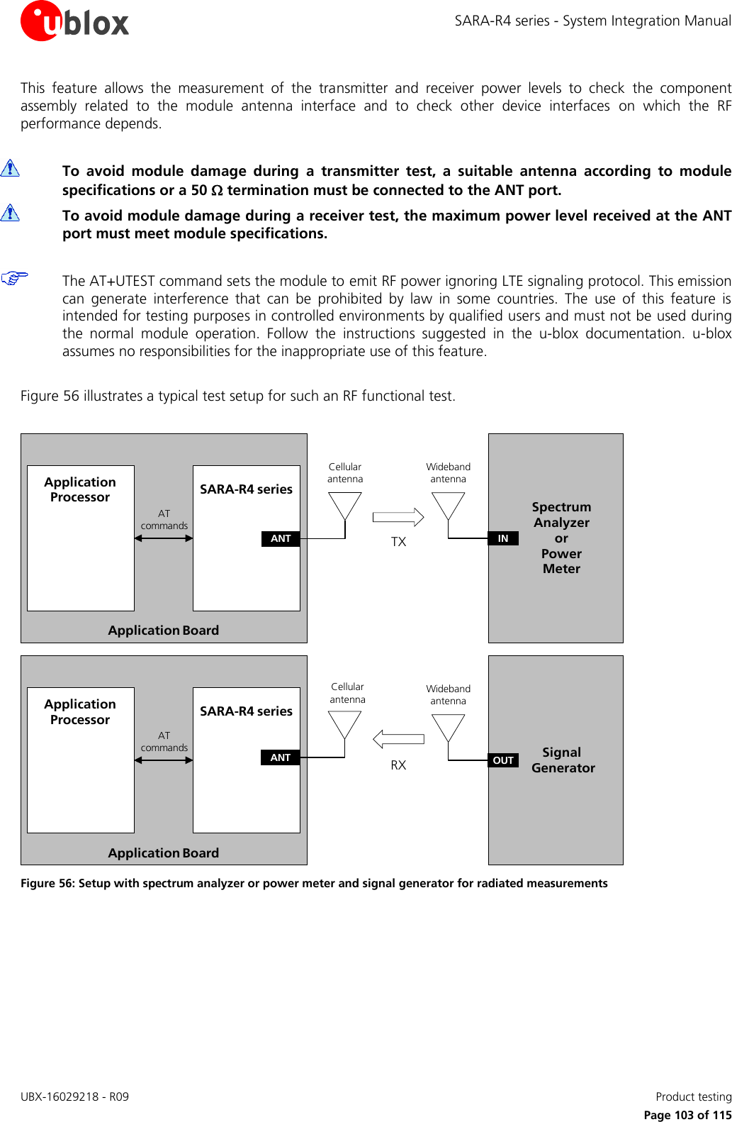
![SARA-R4 series - System Integration Manual UBX-16029218 - R09 Appendix Page 104 of 115 Appendix A Migration between SARA modules A.1 Overview The SARA-G3 2G modules, the SARA-U2 3G / 2G modules, the SARA-R4 LTE Cat M1/NB1 / 2G modules and the SARA-N2 LTE Cat NB1 modules have exactly the same u-blox SARA form factor (26.0 x 16.0 mm, 96-pin LGA), with compatible pin assignments, as shown in Figure 57. Any one of the modules can be mounted on a single application board using exactly the same copper mask, solder mask and paste mask. 64 63 61 60 58 57 55 5422 23 25 26 28 29 31 3211108754212119181615131243444647495052533335363839414265 66 67 68 69 7071 72 73 74 75 7677 7879 8081 8283 8485 86 87 88 89 9091 92 93 94 95 96CTSRTSDCDRIV_INTRSVDGNDGPIO6RESET_NGPIO1PWR_ONRXDTXD32017149624 27 305148454037345962 56GNDGNDDSRDTRGNDVUSB_DETGNDGNDUSB_D-USB_D+RSVDGNDGPIO2GPIO3SDASCLGPIO4GNDGNDGNDSDIO_D2SDIO_CMDSDIO_D0SDIO_D1GNDVCCVCCRSVDI2S_TXD/SPI_CSI2S_CLK/SPI_CLKSIM_CLKSIM_IOVSIMGPIO5VCCSDIO_D3SDIO_CLKSIM_RSTI2S_RXD/SPI_MISOI2S_WA/SPI_MOSIGNDGNDGNDGNDGNDGNDGNDGNDGNDANT_DETANTSARA-R4Top ViewPin 65-96: GND64 63 61 60 58 57 55 5422 23 25 26 28 29 31 3211108754212119181615131243444647495052533335363839414265 66 67 68 69 7071 72 73 74 75 7677 7879 8081 8283 8485 86 87 88 89 9091 92 93 94 95 96CTSRTSDCDRIV_INTV_BCKPGNDRSVDRESET_NGPIO1PWR_ONRXDTXD32017149624 27 305148454037345962 56GNDGNDDSRDTRGNDRSVDGNDGNDRXD_AUXTXD_AUXRSVDGNDGPIO2GPIO3SDASCLGPIO4GNDGNDGNDSPK_PMIC_BIASMIC_GNDMIC_PGNDVCCVCCRSVDI2S_TXDI2S_CLKSIM_CLKSIM_IOVSIMSIM_DETVCCMIC_NSPK_NSIM_RSTI2S_RXDI2S_WAGNDGNDGNDGNDGNDGNDGNDGNDGNDANT_DETANTSARA-G3Top ViewPin 65-96: GND64 63 61 60 58 57 55 5422 23 25 26 28 29 31 3211108754212119181615131243444647495052533335363839414265 66 67 68 69 7071 72 73 74 75 7677 7879 8081 8283 8485 86 87 88 89 9091 92 93 94 95 96CTSRTSDCDRIV_INTV_BCKPGNDCODEC_CLKRESET_NGPIO1PWR_ONRXDTXD32017149624 27 305148454037345962 56GNDGNDDSRDTRGNDVUSB_DETGNDGNDUSB_D-USB_D+RSVDGNDGPIO2GPIO3SDASCLGPIO4GNDGNDGNDRSVDRSVDRSVDRSVDGNDVCCVCCRSVDI2S_TXDI2S_CLKSIM_CLKSIM_IOVSIMSIM_DETVCCRSVDRSVDSIM_RSTI2S_RXDI2S_WAGNDGNDGNDGNDGNDGNDGNDGNDGNDANT_DETANTSARA-U2Top ViewPin 65-96: GND64 63 61 60 58 57 55 5422 23 25 26 28 29 31 3211108754212119181615131243444647495052533335363839414265 66 67 68 69 7071 72 73 74 75 7677 7879 8081 8283 8485 86 87 88 89 9091 92 93 94 95 96CTSRTSRSVDRSVDV_INTRSVDGNDRSVDRESET_NGPIO1RSVDRXDTXD32017149624 27 305148454037345962 56GNDGNDRSVDRSVDGNDRSVDGNDGNDRSVDRSVDRSVDGNDRSVDGPIO2SDASCLRSVDGNDGNDGNDRSVDRSVDRSVDRSVDGNDVCCVCCRSVDRSVDRSVDSIM_CLKSIM_IOVSIMRSVDVCCRSVDRSVDSIM_RSTRSVDRSVDGNDGNDGNDGNDGNDGNDGNDGNDGNDANT_DETANTSARA-N2Top ViewPin 65-96: GND Figure 57: SARA-G3, SARA-U2, SARA-R4 and SARA-R4 series modules’ layout and pin assignment SARA modules are also form-factor compatible with the u-blox LISA, LARA and TOBY cellular module families: although each has a different form factor, the footprints for the TOBY, LISA, SARA and LARA modules have been developed to ensure layout compatibility. With the u-blox “nested design” solution, any TOBY, LISA, SARA or LARA module can be alternatively mounted on the same space of a single “nested” application board as described in Figure 58. Guidelines for implementing a nested application board, a description of the u-blox reference nested design and a comparison between the TOBY, LISA, SARA and LARA modules are provided in the Nested Design Application Note [21]. LISA cellular moduleLARA cellular moduleSARA cellular moduleNested application boardTOBY cellular module Figure 58: TOBY, LISA, SARA, LARA modules’ layout compatibility: all modules are accommodated on the same nested footprint](https://usermanual.wiki/u-blox/2AGQN4NNN.User-Manual-2/User-Guide-3940431-Page-104.png)
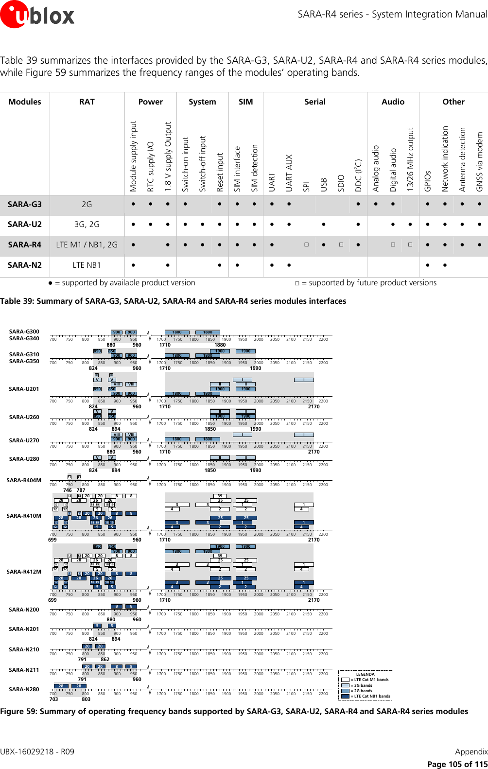
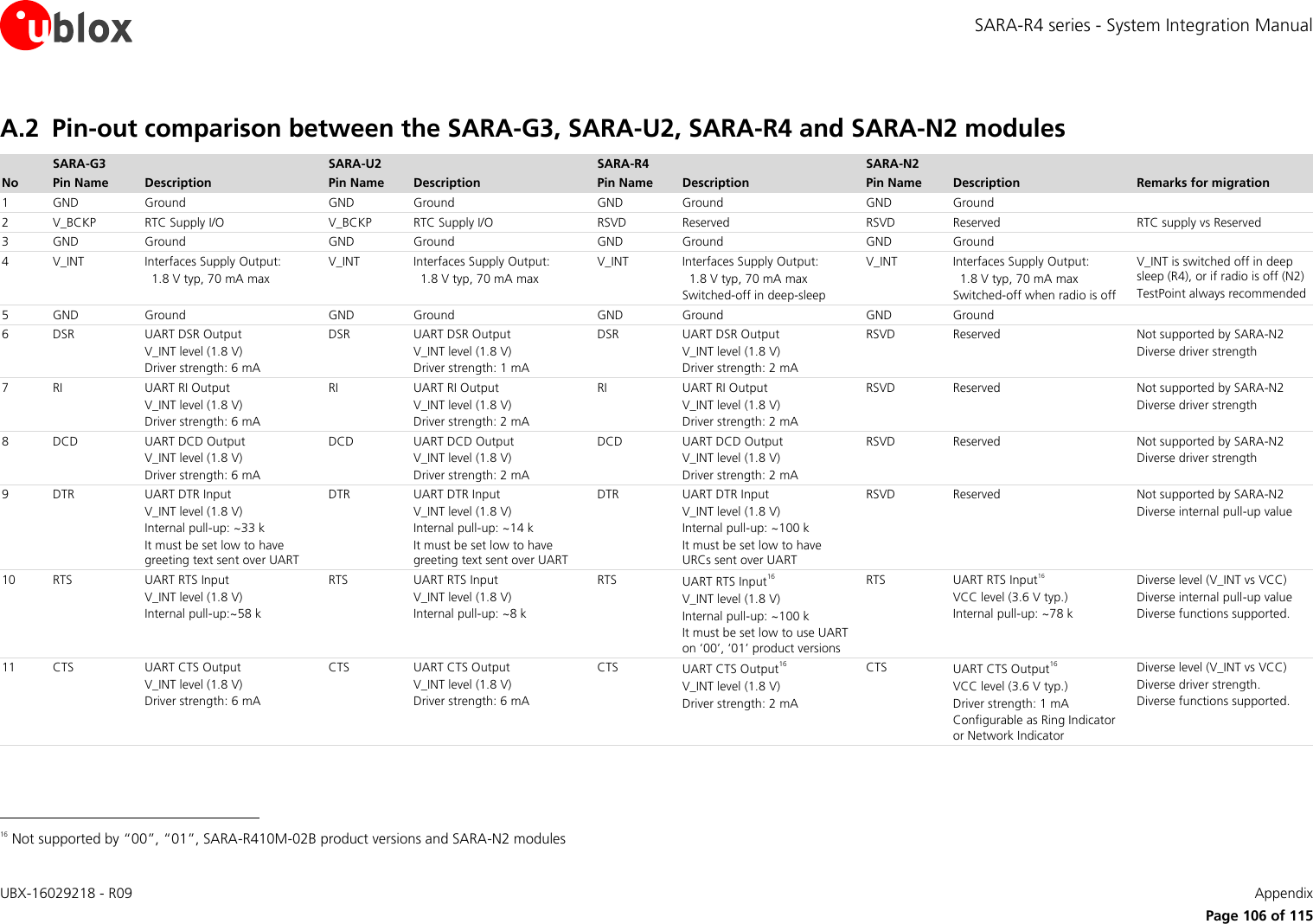
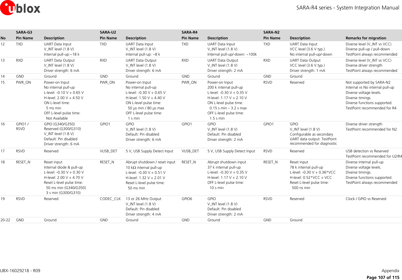
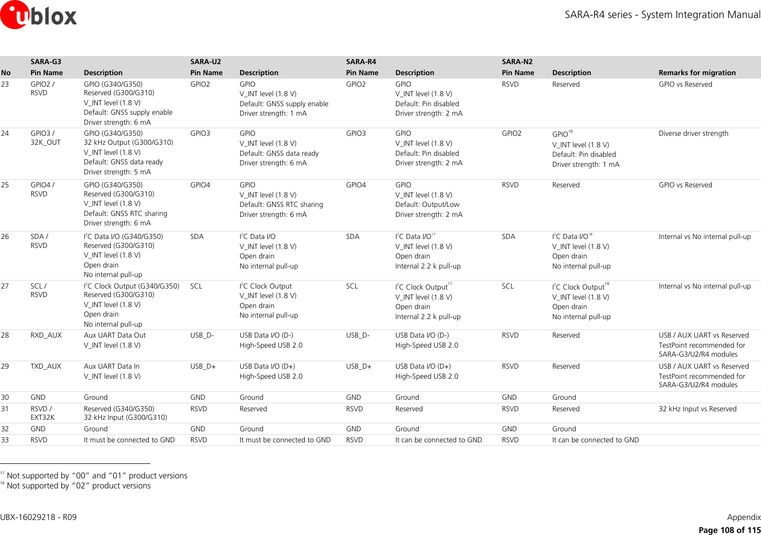
![SARA-R4 series - System Integration Manual UBX-16029218 - R09 Appendix Page 109 of 115 SARA-G3 SARA-U2 SARA-R4 SARA-N2 No Pin Name Description Pin Name Description Pin Name Description Pin Name Description Remarks for migration 34 I2S_WA / RSVD I2S Word Align.(G340/G350) Reserved (G300/G310) V_INT level (1.8 V) Driver strength: 6 mA I2S_WA I2S Word Alignment V_INT level (1.8 V) Driver strength: 2 mA I2S_WA / SPI_MOSI I2S Word Alignm19 / SPI MOSI19 V_INT level (1.8 V) Driver strength: 2 mA RSVD Reserved I2S vs SPI vs Reserved 35 I2S_TXD / RSVD I2S Data Output (G340/G350) Reserved (G300/G310) V_INT level (1.8 V) Driver strength: 5 mA I2S_TXD I2S Data Output V_INT level (1.8 V) Driver strength: 2 mA I2S_TXD / SPI_CS I2S Data Out19 / SPI chip select19 V_INT level (1.8 V) Driver strength: 2 mA RSVD Reserved I2S vs SPI vs Reserved 36 I2S_CLK / RSVD I2S Clock (G340/G350) Reserved (G300/G310) V_INT level (1.8 V) Driver strength: 5 mA I2S_CLK I2S Clock V_INT level (1.8 V) Driver strength: 2 mA I2S_CLK / SPI_CLK I2S Clock19 / SPI clock19 V_INT level (1.8 V) Driver strength: 2 mA RSVD Reserved I2S vs SPI vs Reserved 37 I2S_RXD / RSVD I2S Data Input (G340/G350) Reserved (G300/G310) V_INT level (1.8 V) I2S_RXD I2S Data Input V_INT level (1.8 V) I2S_RXD / SPI_MISO I2S Data Input19 / SPI MISO19 V_INT level (1.8 V) RSVD Reserved I2S vs SPI vs Reserved 38 SIM_CLK 1.8V/3V SIM Clock Output SIM_CLK 1.8V/3V SIM Clock Output SIM_CLK 1.8V/3V SIM Clock Output SIM_CLK 1.8V SIM Clock Output 39 SIM_IO 1.8V/3V SIM Data I/O Internal 4.7 k pull-up SIM_IO 1.8V/3V SIM Data I/O Internal 4.7 k pull-up SIM_IO 1.8V/3V SIM Data I/O Internal 4.7 k pull-up SIM_IO 1.8V SIM Data I/O Internal 4.7 k pull-up 40 SIM_RST 1.8V/3V SIM Reset Output SIM_RST 1.8V/3V SIM Reset Output SIM_RST 1.8V/3V SIM Reset Output SIM_RST 1.8V SIM Reset Output 41 VSIM 1.8V/3V SIM Supply Output VSIM 1.8V/3V SIM Supply Output VSIM 1.8V/3V SIM Supply Output VSIM 1.8V SIM Supply Output 42 SIM_DET SIM Detection Input V_INT level (1.8 V) SIM_DET SIM Detection Input V_INT level (1.8 V) GPIO5 SIM Detection Input V_INT level (1.8 V) RSVD Reserved SIM Detection vs Reserved 43 GND Ground GND Ground GND Ground GND Ground 44 SPK_P / RSVD Analog Audio Out (+) / Reserved RSVD Reserved SDIO_D2 SDIO serial data [2]19 RSVD Reserved Analog Audio vs SDIO vs RSVD 45 SPK_N / RSVD Analog Audio Out (-) / Reserved RSVD Reserved SDIO_CLK SDIO serial clock19 RSVD Reserved Analog Audio vs SDIO vs RSVD 46 MIC_BIAS / RSVD Microphone Supply Out / Reserved RSVD Reserved SDIO_CMD SDIO command19 RSVD Reserved Analog Audio vs SDIO vs RSVD 47 MIC_GND / RSVD Microphone Ground / Reserved RSVD Reserved SDIO_D0 SDIO serial data [0]19 RSVD Reserved Analog Audio vs SDIO vs RSVD 48 MIC_N / RSVD Analog Audio In (-) / Reserved RSVD Reserved SDIO_D3 SDIO serial data [3]19 RSVD Reserved Analog Audio vs SDIO vs RSVD 49 MIC_P / RSVD Analog Audio In (+) / Reserved RSVD Reserved SDIO_D1 SDIO serial data [1]19 RSVD Reserved Analog Audio vs SDIO vs RSVD 50 GND Ground GND Ground GND Ground GND Ground 19 Not supported by “00”, “01” and “02” product version](https://usermanual.wiki/u-blox/2AGQN4NNN.User-Manual-2/User-Guide-3940431-Page-109.png)
![SARA-R4 series - System Integration Manual UBX-16029218 - R09 Appendix Page 110 of 115 SARA-G3 SARA-U2 SARA-R4 SARA-N2 No Pin Name Description Pin Name Description Pin Name Description Pin Name Description Remarks for migration 51-53 VCC Module Supply Input Normal op. range: 3.35 V – 4.5 V Extended op. range: 3.00 V – 4.5 V Current consumption: ~2.0A pulse current in 2G (recommended ≥100uF cap.) Switch-on by applying VCC VCC Module Supply Input Normal op. range: 3.3 V – 4.4 V Extended op. range: 3.1 V – 4.5 V Current consumption: ~2.0A pulse current in 2G (recommended ≥100uF cap.) Ferrite bead for GHz noise recommended for U201 Switch-on by applying VCC VCC Module Supply Input Normal op. range: 3.2 V – 4.2 V Extended op. range: 3.0 V – 4.3 V Current consumption: ~2.0A pulse current in 2G (recommended ≥100uF cap.) ~0.5A pulse current in LTE (recommended ≥10uF cap.) No switch-on by applying VCC VCC Module Supply Input Normal op. range: 3.1 V – 4.0 V Extended op. range: 2.75 V – 4.2 V Current consumption: ~0.3A pulse current in NB-IoT (recommended ≥100uF cap.) Switch-on by applying VCC Diverse voltage levels. Diverse current consumption. Diverse recommended external capacitors and other parts. Regular pF / nF recommended Diverse functions supported. 54-55 GND Ground GND Ground GND Ground GND Ground 56 ANT RF Antenna I/O ANT RF Antenna I/O ANT RF Antenna I/O ANT RF Antenna I/O Diverse bands supported (summarized in Figure 59) 57-61 GND Ground GND Ground GND Ground GND Ground 62 ANT_DET / RSVD Antenna Detection Input / Reserved ANT_DET Antenna Detection Input ANT_DET Antenna Detection Input ANT_DET Antenna Detection Input20 Antenna Detection vs Reserved 63-96 GND Ground GND Ground GND Ground GND Ground Table 40: SARA-G3, SARA-U2, SARA-R4 and SARA-N2 series modules pin assignments with remarks for migration For further details regarding the characteristics, capabilities, usage or settings applicable for each interface of the SARA-G3, SARA-U2, SARA-R4 and SARA-N2 series cellular modules, see the related Data Sheet [1], [16], [17], [18], the related System Integration Manual [19], [20], and the Nested Design Application Note [21]. 20 Not supported by “02” product version](https://usermanual.wiki/u-blox/2AGQN4NNN.User-Manual-2/User-Guide-3940431-Page-110.png)
![SARA-R4 series - System Integration Manual UBX-16029218 - R09 Related documents Page 113 of 115 Related documents [1] u-blox SARA-R4 series Data Sheet, document number UBX-16024152 [2] u-blox SARA-R4 series AT Commands Manual, document number UBX-17003787 [3] u-blox EVK-R4 User Guide, document number UBX-16029216 [4] Universal Serial Bus Revision 2.0 specification, http://www.usb.org/developers/docs/usb20_docs/ [5] ITU-T Recommendation V.24 - 02-2000 - List of definitions for interchange circuits between Data Terminal Equipment (DTE) and Data Circuit-terminating Equipment (DCE), http://www.itu.int/rec/T-REC-V.24-200002-I/en [6] 3GPP TS 27.007 - AT command set for User Equipment (UE) [7] 3GPP TS 27.005 - Use of Data Terminal Equipment - Data Circuit terminating; Equipment (DTE - DCE) interface for Short Message Service (SMS) and Cell Broadcast Service (CBS) [8] 3GPP TS 27.010 - Terminal Equipment to User Equipment (TE-UE) multiplexer protocol [9] I2C-bus specification and user manual - Rev. 5 - 9 October 2012 - NXP Semiconductors, http://www.nxp.com/documents/user_manual/UM10204.pdf [10] GSM Association TS.09 - Battery Life Measurement and Current Consumption Technique, https://www.gsma.com/newsroom/wp-content/uploads//TS.09_v10.0.pdf [11] 3GPP TS 36.521-1 - Evolved Universal Terrestrial Radio Access; User Equipment conformance specification; Radio transmission and reception; Part 1: Conformance Testing [12] 3GPP TS 36.521-2 - Evolved Universal Terrestrial Radio Access (E-UTRA); User Equipment conformance specification; Radio transmission and reception; Part 2: Implementation Conformance Statement (ICS) [13] 3GPP TS 36.523-2 - Evolved Universal Terrestrial Radio Access (E-UTRA) and Evolved Packet Core (EPC); User Equipment conformance specification; Part 2: Implementation Conformance Statement (ICS) [14] u-blox End user test Application Note, document number UBX-13001922 [15] u-blox Package Information Guide, document number UBX-14001652 [16] u-blox SARA-G3 series Data Sheet, document number UBX-13000993 [17] u-blox SARA-U2 series Data Sheet, document number UBX-13005287 [18] u-blox SARA-N2 series Data Sheet, document number UBX-15025564 [19] u-blox SARA-G3 / SARA-U2 series System Integration Manual, document number UBX-13000995 [20] u-blox SARA-N2 series System Integration Manual, document number UBX-17005143 [21] u-blox Nested Design Application Note, document number UBX-16007243 Some of the above documents can be downloaded from the u-blox web-site (http://www.u-blox.com/).](https://usermanual.wiki/u-blox/2AGQN4NNN.User-Manual-2/User-Guide-3940431-Page-113.png)