dresden elektronik ingenieurtechnik MEGA23M12 2.4GHz IEEE 802.15.4 compliant radio module User Manual 15 MEGA23M12 User Manual
dresden elektronik ingenieurtechnik gmbh 2.4GHz IEEE 802.15.4 compliant radio module 15 MEGA23M12 User Manual
Contents
- 1. 15_MEGA23M12_User _Manual
- 2. 15_MEGA23M12_UserMan
- 3. Users Manual
15_MEGA23M12_User _Manual
![User Manual Version 1.3 2013-06-10 OEM radio modules deRFmega www.dresden-elektronik.de Page 5 of 69 Abbreviations Abbreviation Description IEEE 802.15.4 IEEE 802.15.4 standard, applicable to low-rate Wireless Personal Area Networks (WPAN) 6LoWPAN IPv6 over Low Power Wireless Personal Area Networks ADC Analog to Digital Converter CE Consumer Electronics EMI Electromagnetic Interference ETSI European Telecommunications Standards Institute FCC Federal Communications Commission GPIO Generals Purpose Input Output JTAG Joint Test Action Group, digital interface for debugging of embedded devices, also known as IEEE 1149.1 standard interface ISA SP100 International Society of Automation, the Committee establishes standards and related technical information for implementing wireless systems. ISP In-System-Programming LGA Land Grid Array, a type of surface-mount packaging for integrated circuits LNA Low Noise Amplifier MAC Medium (Media) Access Control MCU, µC Microcontroller Unit PA Power Amplifier PCB Printed Circuit Board PWM Pulse Width Modulation RF Radio Frequency R&TTE Radio and Telecommunications Terminal Equipment (Directive of the European Union) SPI Serial Peripheral Interface TWI Two-Wire Serial Interface U[S]ART Universal [Synchronous/]Asynchronous Receiver Transmitter USB Universal Serial Bus ZigBee Low-cost, low-power wireless mesh network standard. The ZigBee Alliance is a group of companies that maintain and publish the ZigBee standard.](https://usermanual.wiki/dresden-elektronik-ingenieurtechnik/MEGA23M12.15-MEGA23M12-User-Manual/User-Guide-2047839-Page-5.png)
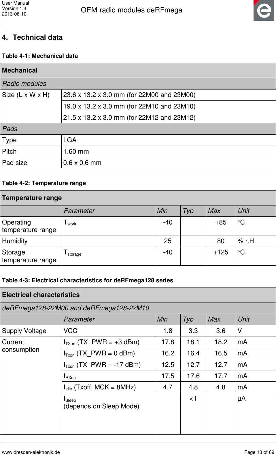
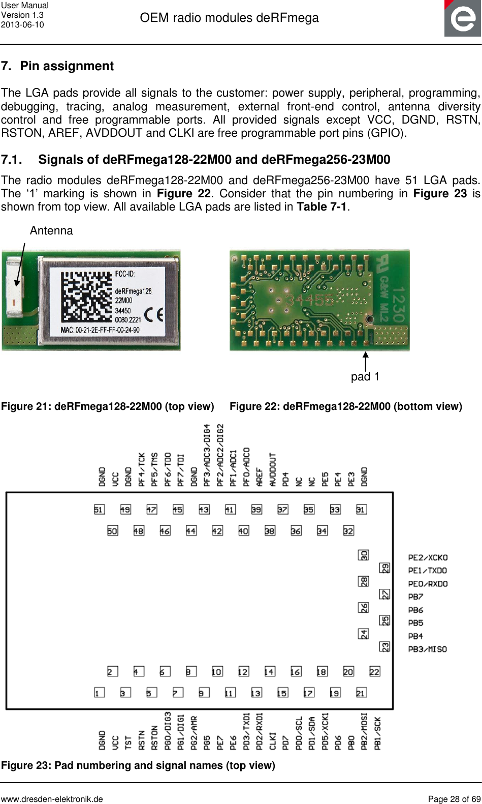
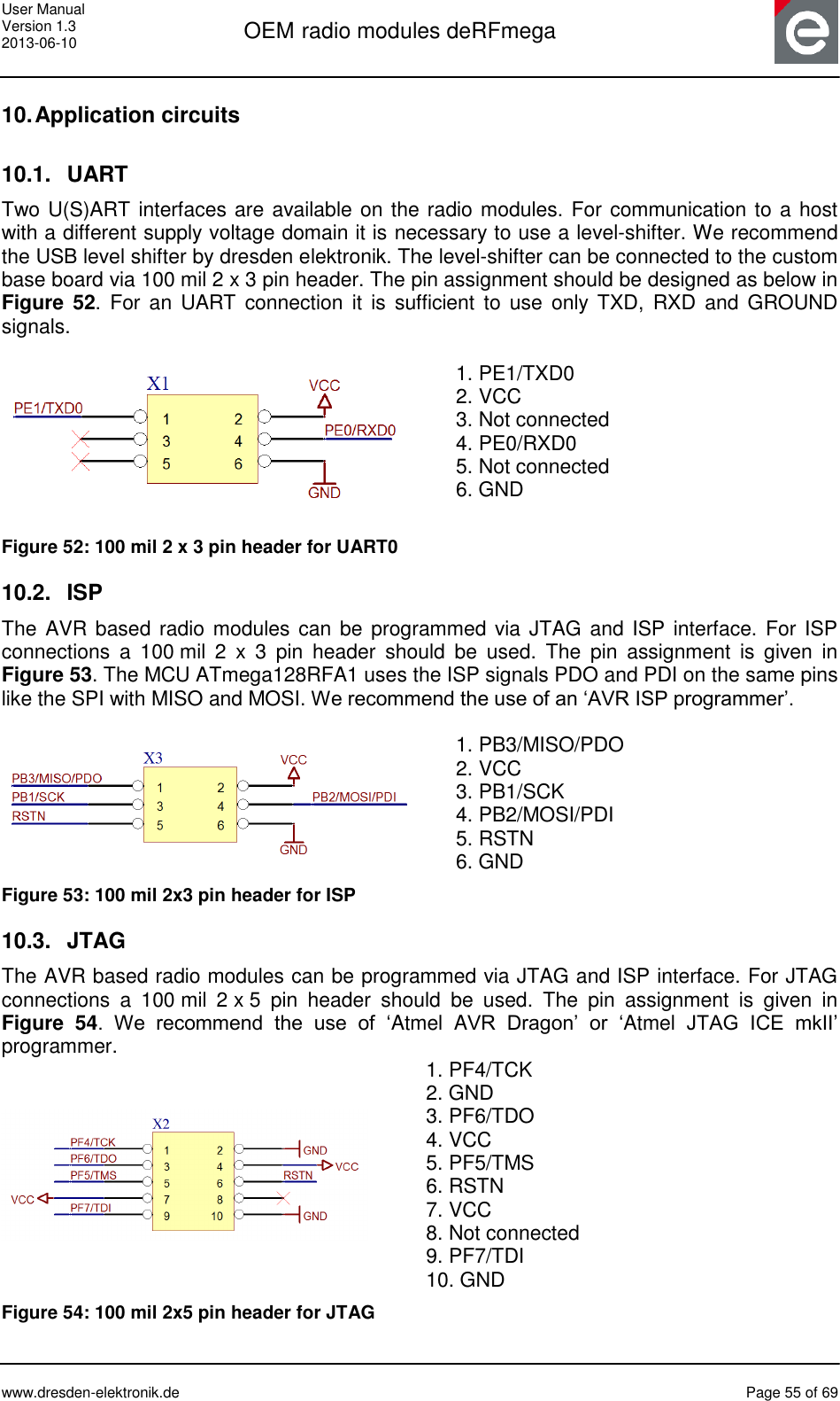
![User Manual Version 1.3 2013-06-10 OEM radio modules deRFmega www.dresden-elektronik.de Page 7 of 69 3. Features 3.1. deRFmega128-22M00 The radio module deRFmega128-22M00 offers the following features: Tiny size: 23.6 x 13.2 x 3.0 mm 51 LGA pads 0.6 x 0.6 mm Supply voltage 1.8 V to 3.6 V RF shielding Onboard 32.768 kHz crystal (Deep-Sleep clock) and 16 MHz crystal Application interfaces: 2x UART, 1x TWI, 1x ADC GPIO interface Debug/Programming interfaces: 1x SPI, 1x JTAG, 1x ISP Onboard 2.4 GHz chip antenna Certification: CE, FCC Figure 1 shows the block diagram of the radio module deRFmega128-22M00. ATmega128RFA1Transceiver crystal16MHz [+/-10ppm]JTAGUARTVCC1.8V to 3.6VWatch crystal32.768kHzSPITWIADCGPIO2.4GHz antenna Figure 1: Block diagram deRFmega128-22M00](https://usermanual.wiki/dresden-elektronik-ingenieurtechnik/MEGA23M12.15-MEGA23M12-User-Manual/User-Guide-2047839-Page-7.png)
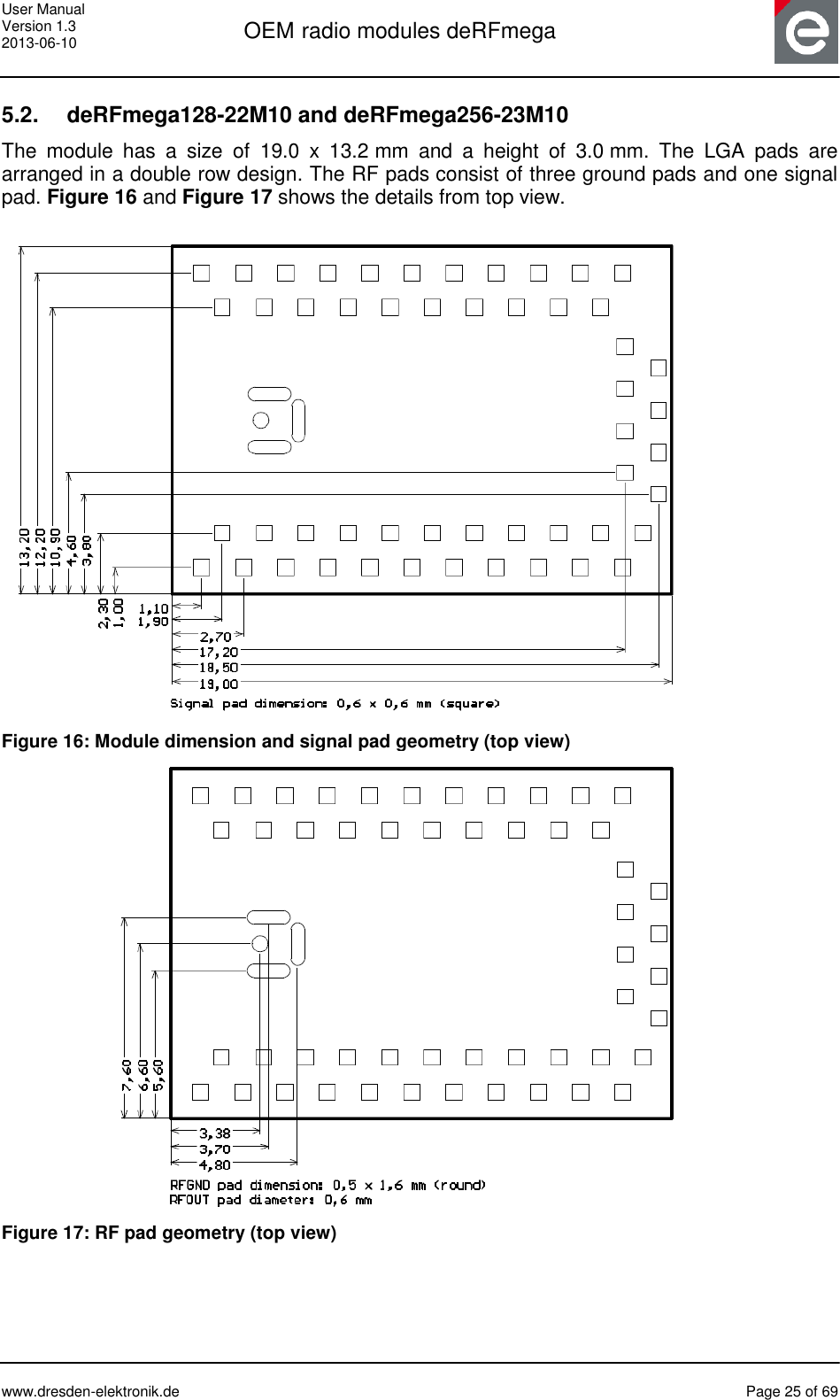
![User Manual Version 1.3 2013-06-10 OEM radio modules deRFmega www.dresden-elektronik.de Page 8 of 69 3.2. deRFmega128-22M10 The radio module deRFmega128-22M10 offers the following features: Tiny size: 19.0 x 13.2 x 3.0 mm 55 LGA pads 0.6 x 0.6 mm Supply voltage 1.8 V to 3.6 V RF shielding Onboard 32.768 kHz crystal (Deep-Sleep clock) and 16 MHz crystal Application interfaces: 2x UART, 1x TWI, 1x ADC GPIO interface Debug/Programming interfaces: 1x SPI, 1x JTAG, 1x ISP Solderable 2.4 GHz RF output pads (1x RFOUT, 3x RFGND) Certification: CE, FCC pending Figure 2 shows the block diagram of the radio module deRFmega128-22M10. ATmega128RFA1Transceiver crystal16MHz [+/-10ppm]JTAGUARTVCC1.8V to 3.6VWatch crystal32.768kHzSPITWIADCGPIORFout Figure 2: Block diagram deRFmega128-22M10](https://usermanual.wiki/dresden-elektronik-ingenieurtechnik/MEGA23M12.15-MEGA23M12-User-Manual/User-Guide-2047839-Page-8.png)
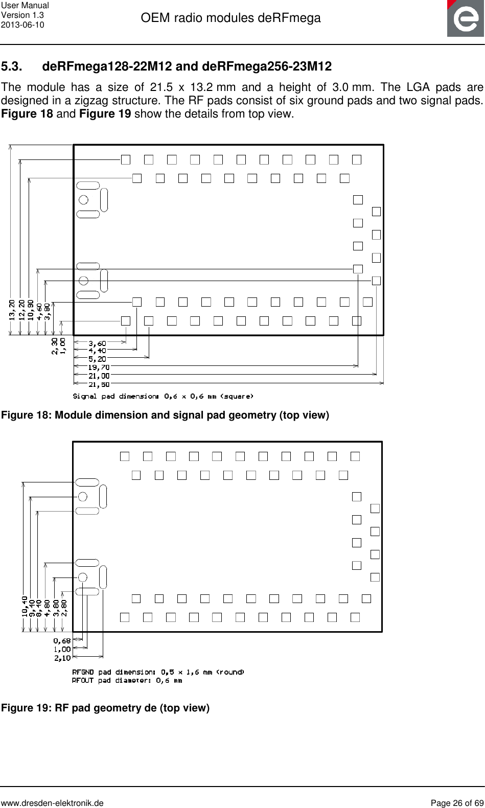
![User Manual Version 1.3 2013-06-10 OEM radio modules deRFmega www.dresden-elektronik.de Page 9 of 69 3.3. deRFmega128-22M12 The radio module deRFmega128-22M12 offers the following features: Tiny size: 21.5 x 13.2 x 3.0 mm 59 LGA pads 0.6 x 0.6 mm Supply voltage 2.0 V to 3.6 V Antenna diversity support RF shielding Onboard 32.768 kHz crystal (Deep-Sleep clock) and 16 MHz crystal Application interfaces: 2x UART, 1x TWI GPIO interface Debug/Programming interfaces: 1x SPI, 1x JTAG, 1x ISP 2.4 GHz front-end module with internal 20 dB PA and LNA Solderable 2.4 GHz RF output pad (2x RFOUT, 6x RFGND) Certification: CE, FCC pending Figure 3 shows the block diagram of the radio module deRFmega128-22M12. Figure 3: Block diagram deRFmega128-22M12 ATmega128RFA1Transceiver crystal16MHz [+/-10ppm]JTAGUARTVCC2.0V to 3.6VWatch crystal32.768kHzSPITWIADCGPIO2.4GHz Front-End RFout 1RFout 2RFControl](https://usermanual.wiki/dresden-elektronik-ingenieurtechnik/MEGA23M12.15-MEGA23M12-User-Manual/User-Guide-2047839-Page-9.png)
![User Manual Version 1.3 2013-06-10 OEM radio modules deRFmega www.dresden-elektronik.de Page 10 of 69 3.4. deRFmega256-23M00 The radio module deRFmega256-23M00 offers the following features: Tiny size: 23.6 x 13.2 x 3.0 mm 51 LGA pads 0.6 x 0.6 mm Supply voltage 1.8 V to 3.6 V RF shielding Onboard 32.768 kHz crystal (Deep-Sleep clock) and 16 MHz crystal Application interfaces: 2x UART, 1x TWI, 1x ADC GPIO interface Debug/Programming interfaces: 1x SPI, 1x JTAG, 1x ISP Onboard 2.4 GHz chip antenna Certification: CE, FCC pending Figure 4 shows the block diagram of the radio module deRFmega256-23M00. ATmega256RFR2Transceiver crystal16MHz [+/-10ppm]JTAGUARTVCC1.8V to 3.6VWatch crystal32.768kHzSPITWIADCGPIO2.4GHz antenna Figure 4: Block diagram deRFmega256-23M00](https://usermanual.wiki/dresden-elektronik-ingenieurtechnik/MEGA23M12.15-MEGA23M12-User-Manual/User-Guide-2047839-Page-10.png)
![User Manual Version 1.3 2013-06-10 OEM radio modules deRFmega www.dresden-elektronik.de Page 11 of 69 3.5. deRFmega256-23M10 The radio module deRFmega256-23M10 offers the following features: Tiny size: 19.0 x 13.2 x 3.0 mm 55 LGA pads 0.6 x 0.6 mm Supply voltage 1.8 V to 3.6 V RF shielding Onboard 32.768 kHz crystal (Deep-Sleep clock) and 16 MHz crystal Application interfaces: 2x UART, 1x TWI, 1x ADC GPIO interface Debug/Programming interfaces: 1x SPI, 1x JTAG, 1x ISP Solderable 2.4 GHz RF output pads (1x RFOUT, 3x RFGND) Certification: CE, FCC pending Figure 5 shows the block diagram of the radio module deRFmega256-23M10. ATmega256RFR2Transceiver crystal16MHz [+/-10ppm]JTAGUARTVCC1.8V to 3.6VWatch crystal32.768kHzSPITWIADCGPIORFout Figure 5: Block diagram deRFmega256-23M10](https://usermanual.wiki/dresden-elektronik-ingenieurtechnik/MEGA23M12.15-MEGA23M12-User-Manual/User-Guide-2047839-Page-11.png)
![User Manual Version 1.3 2013-06-10 OEM radio modules deRFmega www.dresden-elektronik.de Page 12 of 69 3.6. deRFmega256-23M12 The radio module deRFmega256-23M12 offers the following features: Tiny size: 21.5 x 13.2 x 3.0 mm 59 LGA pads 0.6 x 0.6 mm Supply voltage 2.0 V to 3.6 V Antenna diversity support RF shielding Onboard 32.768 kHz crystal (Deep-Sleep clock) and 16 MHz crystal Application interfaces: 2x UART, 1x TWI GPIO interface Debug/Programming interfaces: 1x SPI, 1x JTAG, 1x ISP 2.4 GHz front-end module with internal 20 dB PA and LNA Solderable 2.4 GHz RF output pad (2x RFOUT, 6x RFGND) Certification: CE, FCC pending Figure 6 shows the block diagram of the radio module deRFmega256-23M12. ATmega256RFR2Transceiver crystal16MHz [+/-10ppm]JTAGUARTVCC2.0V to 3.6VWatch crystal32.768kHzSPITWIADCGPIO2.4GHz Front-End RFout 1RFout 2RFControl Figure 6: Block diagram deRFmega256-23M12](https://usermanual.wiki/dresden-elektronik-ingenieurtechnik/MEGA23M12.15-MEGA23M12-User-Manual/User-Guide-2047839-Page-12.png)
![User Manual Version 1.3 2013-06-10 OEM radio modules deRFmega www.dresden-elektronik.de Page 23 of 69 4.5. Output power and duty cycle settings for power amplified radio modules The radio modules deRFmega128-22M12 and deRFmega256-23M12 are able to provide an output power greater than 20dBm. Table 4-10 defines the necessary power settings of the TX_PWR register [1] and [2], which must be set to fulfill all national requirements of Europe (EN 300 328) and USA (CFR 47 Ch. I FCC Part 15). The duty cycle defines the relationship between the radio-on time and the period of 100ms. Table 4-10: power table for deRFmega128-22M12 Device deRFmega128-22M12 deRFmega256-23M12 Channel ETSI FCC ETSI FCC TX_PWR [hex] Duty Cycle [%] TX_PWR [hex] Duty Cycle [%] TX_PWR [hex] Duty Cycle [%] TX_PWR [hex] Duty Cycle [%] 11 0xE 100 0xB 100 0xF 100 0xD 100 12 0xE 100 0x2 100 0xF 100 0x8 100 13 0xE 100 0x1 100 0xF 100 0x4 100 14 0xE 100 0x0 100 0xF 100 0x4 100 15 0xE 100 0x0 100 0xF 100 0x4 100 16 0xE 100 0x0 100 0xF 100 0x4 100 17 0xE 100 0x0 100 0xF 100 0x4 100 18 0xE 100 0x0 100 0xF 100 0x4 100 19 0xE 100 0x0 100 0xF 100 0x4 100 20 0xE 100 0x0 100 0xF 100 0x4 100 21 0xE 100 0x0 100 0xF 100 0x4 100 22 0xE 100 0x0 100 0xF 100 0x4 100 23 0xE 100 0x6 100 0xF 100 0xA 100 24 0xE 100 0xD 100 0xF 100 0xD 100 25 0xE 100 0xF 100 0xF 100 0xF 100 26 0xE 100 0xF 25 0xF 100 0xF 25](https://usermanual.wiki/dresden-elektronik-ingenieurtechnik/MEGA23M12.15-MEGA23M12-User-Manual/User-Guide-2047839-Page-23.png)
![User Manual Version 1.3 2013-06-10 OEM radio modules deRFmega www.dresden-elektronik.de Page 27 of 69 6. Soldering profile Table 6-1 shows the recommended soldering profile for the radio modules. Table 6-1: Soldering Profile Profile Feature Values Average-Ramp-up Rate (217°C to Peak) 3°C/s max Preheat Temperature 175°C ±25°C 180 s max Temperature Maintained Above 217°C 60 s to 150 s Time within 5°C of Actual Peak Temperature 20 s to 40 s Peak Temperature Range 260°C Ramp-down Rate 6°C/s max Time 25°C to Peak Temperature 8 min max Figure 20 shows a recorded soldering profile for a radio module. The blue colored line illustrates a temperature sensor placed next to the soldering contacts of the radio module. The pink line shows the set temperatures depending on the zone within the reflow soldering machine. 406080100120140160180200220240260280020406080100120140160180200220240260280300320340360t [s]T [°C]Measured Temp. Zone Temp.Figure 20: Recorded soldering profile A solder process without supply of nitrogen causes a discoloration of the metal RF-shielding. It is possible that the placed label shrinks due the reflow process.](https://usermanual.wiki/dresden-elektronik-ingenieurtechnik/MEGA23M12.15-MEGA23M12-User-Manual/User-Guide-2047839-Page-27.png)
![User Manual Version 1.3 2013-06-10 OEM radio modules deRFmega www.dresden-elektronik.de Page 34 of 69 7.2.1. External front-end and antenna diversity control The radio modules deRFmega128-22M10 and deRFmega256-23M10 offer the possibility to control external front-end components and to support antenna diversity. Table 7-3 and Table 7-4 show the logic values of the control signals. A logic ‘0’ is specified with a voltage level of 0 V to 0.3 V. A logic ‘1’ is specified with a value of VCC - 0.3 V to 3.6 V. An application circuit is shown in Section 10.5. Antenna Diversity The antenna diversity algorithm is enabled with setting bit ANT_DIV_EN=1 in the ANT_DIV register. The external control of RF switches must be enabled by bit ANT_EXT_SW_EN of the same register. This action will configure the pins DIG1 and DIG2 as outputs. Both pins are used to feed the RF switch signal and its inverse to the differential inputs of the RF switch. Please refer to ATmega128RFA1 [1] and ATmega256RFR2 [2] datasheet to get information to all register settings. Table 7-3: Antenna diversity control Mode description PG1/DIG1 PF2/DIG2 TRX off Sleep mode Disable register bit ANT_EXT_SW_EN and set port pins DIG1 and DIG2 to output low via I/O port control registers. This action could reduce the power consumption of an external RF switch. ANT0 1 0 ANT1 0 1 Front-End The control of front-end components can be realized with the signals DIG3 and DIG4. The function will be enabled with bit PA_EXT_EN of register TRX_CTRL_1 which configures both pins as outputs. While transmission is turned off DIG3 is set to ‘0’ and DIG4 is set to ‘1’. When the transceiver starts transmission the polarity will be changed. Both pins can be used to control PA, LNA and RF switches. Please refer to ATmega128RFA1 [1] and ATmega256RFR2 [2] datasheet to get information to all register settings. Table 7-4: Front-end control PG0/DIG3 PF3/DIG4 TRX off Sleep mode Disable register bit PA_EXT_EN and set port pins DIG3 and DIG4 to output low via I/O port control registers. This action may reduce the power consumption of external front-end devices. TRX off 0 1 TRX on 1 0 Sleep mode To optimize the power consumption of external front-end components, it is possible to use a dedicated GPIO to set the PA into sleep mode, if applicable or to switch an additionally MOSFET, which supplies the PA.](https://usermanual.wiki/dresden-elektronik-ingenieurtechnik/MEGA23M12.15-MEGA23M12-User-Manual/User-Guide-2047839-Page-34.png)
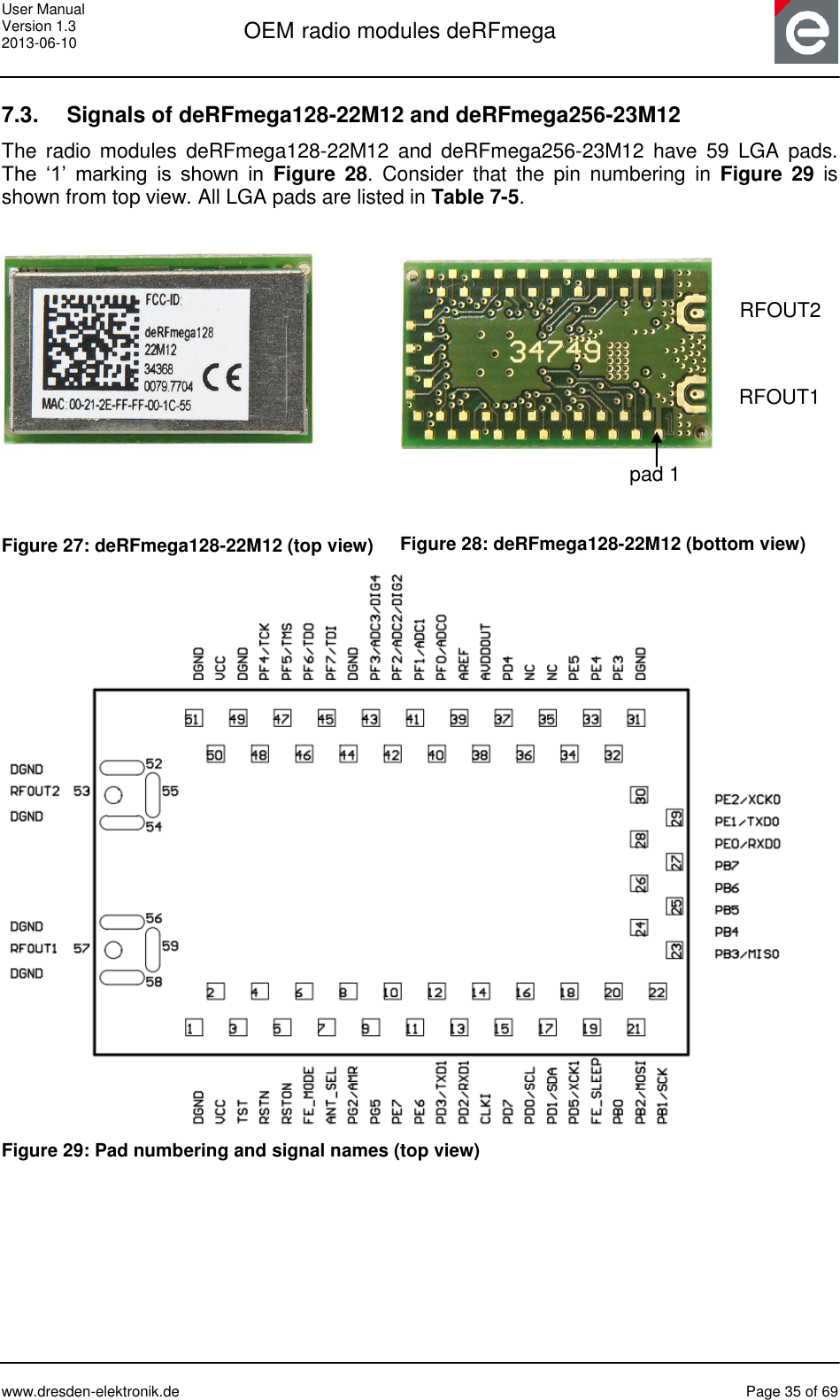
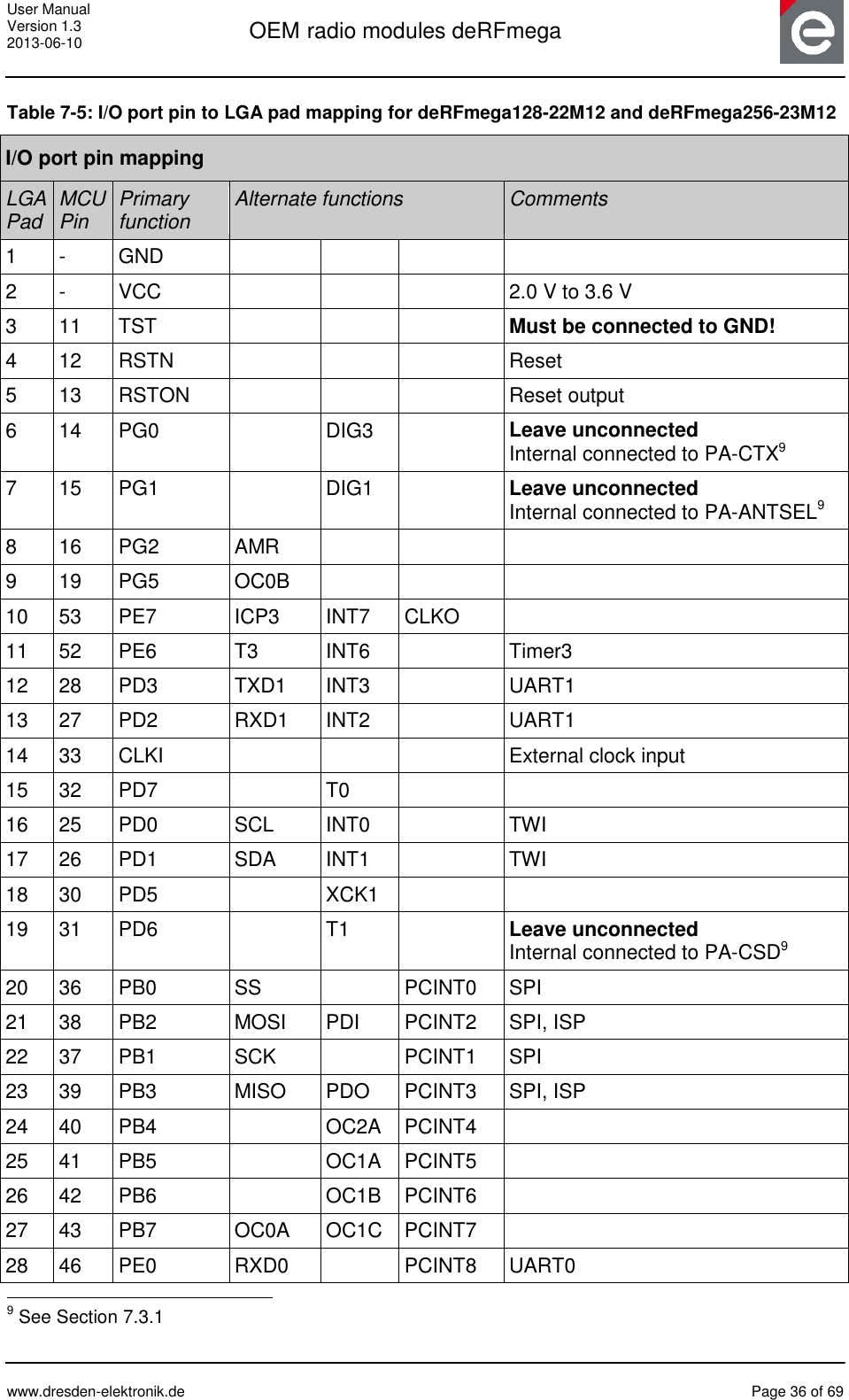
![User Manual Version 1.3 2013-06-10 OEM radio modules deRFmega www.dresden-elektronik.de Page 38 of 69 7.3.1. Internal front-end control The front-end of deRFmega128-22M12 and deRFmega256-23M12 have an internal PA for transmit and a LNA for receive mode. An additionally antenna diversity feature is usable to select the antenna with the best link budget. The front-end control includes three MCU port pins (Figure 30). They are used to choose the TX/RX antenna, de-/activate transmit and receive mode and de-/activate the sleep mode. Table 7-6 and Table 7-7 show the logic values. A logic ‘0’ is specified with a voltage level of 0 V to 0.3 V. A logic ‘1’ is specified with a value of VCC - 0.3 V to 3.6 V. The control signals DIG1, DIG3 and PD6 are available on the LGA pins. Table 7-6: Front-end control of TX/RX and sleep mode Mode description PG1/DIG1 PD6/T1 PG0/DIG3 PA_ANT SEL PA_CSD PA_CTX All off (sleep mode) X 0 0 RX LNA mode X 1 0 TX mode X 1 1 Table 7-7: Front-end control of TX/RX antenna Mode description PG1/DIG1 PD6/T1 PG0/DIG3 PA_ANT SEL PA_CSD PA_CTX RFOUT1 port enabled 0 X X RFOUT2 port enabled 1 X X ATmega128RFA1Transceiver crystal16MHz [+/-10ppm]JTAGUARTVCC2.0V to 3.6VWatch crystal32.768kHzSPITWIADCGPIO RFout 1RFout 2RFDIG1PD6DIG3ANT SELPALNATX/RXSleep Figure 30: Block diagram of front-end functionality and control Note: Do not leave any unused RFOUT pad unterminated! Leave pins DIG1, DIG2, DIG3, DIG4 and PD6 unconnected to ensure the proper front-end functionality!](https://usermanual.wiki/dresden-elektronik-ingenieurtechnik/MEGA23M12.15-MEGA23M12-User-Manual/User-Guide-2047839-Page-38.png)
![User Manual Version 1.3 2013-06-10 OEM radio modules deRFmega www.dresden-elektronik.de Page 39 of 69 7.4. Signal description The available signals are described in Table 7-8. Please refer to ATmega128RFA1 [1] and ATmega256RFR2 [2] datasheet for more information of all dedicated signals. Table 7-8: Signal description list Signal name Function Type Active Level Comments Power VCC Voltage Regulator Power Supply Input Power GND Ground Clocks and Oscillators CLKI External Clock Input Input CLKO Divided System Clock Output Output JTAG TCK Test Clock Input No pull-up resistor on module TDI Test Data In Input No pull-up resistor on module TDO Test Data Out Output TDM Test Mode Select Input No pull-up resistor on module Serial Programming PDI Data Input Input PDO Data Output Output SCK Serial Clock Input Reset RSTN Microcontroller Reset I/O Low Pull-Up resistor10 USART TXD0 – TXD1 Transmit Data RXD0 – RXD1 Receive Data XCK0 – XCK1 Serial Clock Timer/Counter and PWM Controller OC0A-OC3A Output Compare and PWM Output A for Timer/Counter 0 to 3 OC0B-OC3B Output Compare and PWM Output B for Timer/Counter 0 to 3 10 Internal MCU Pull-up resistor](https://usermanual.wiki/dresden-elektronik-ingenieurtechnik/MEGA23M12.15-MEGA23M12-User-Manual/User-Guide-2047839-Page-39.png)
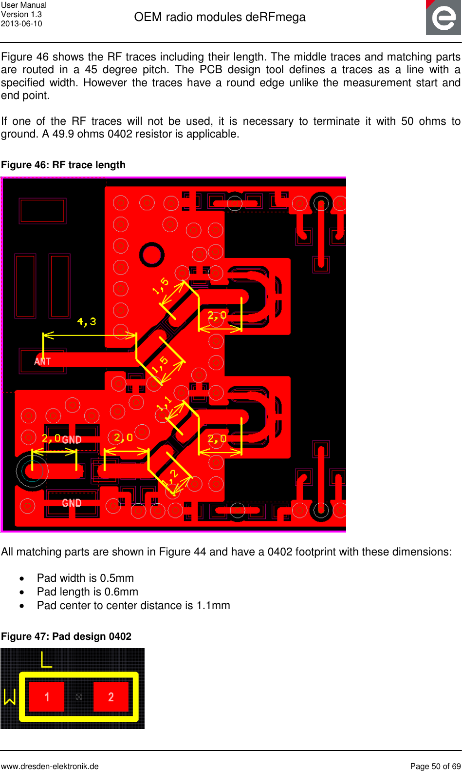
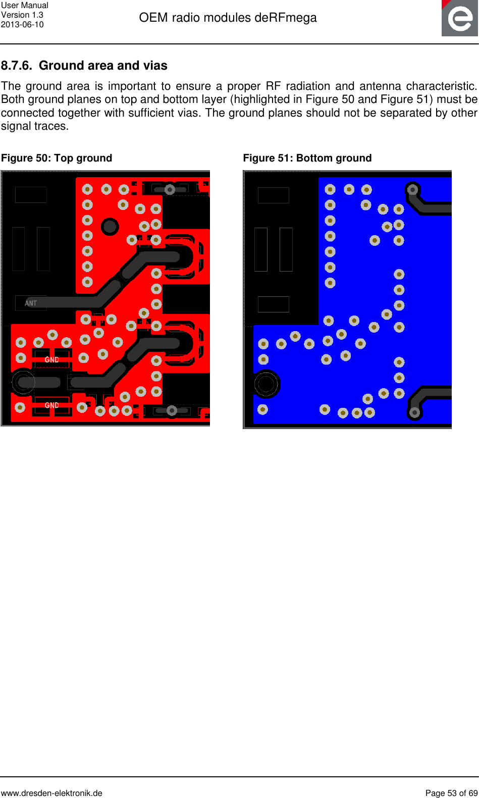
![User Manual Version 1.3 2013-06-10 OEM radio modules deRFmega www.dresden-elektronik.de Page 46 of 69 8.5. Traces Common signal traces should be designed with these guidelines: Traces on top layer are not allowed under the module (see Figure 36) Traces on mid layers and bottom layers are allowed (see Figure 36) Route traces straight away from module (see Figure 33) Do not use heat traps of components directly on the RF trace Do not use 90 degree corners. Better is 45 degree or rounded corners. The trace design for RF signals has a lot of more important points to regard. It defines the trace impedance and therefore the signal reflection and transmission. The most commonly used RF trace designs are Microstrip and Grounded Coplanar Wave Guide (GCPW). The dimension of the trace is depending on the used PCB material, the height of the material to the next ground plane, a PCB with or without a ground plane, the trace width and for GCPW the gap to the top ground plane. The calculation is not trivial, therefore specific literature and web content is available (see [3]) The reference plane to the GCPW should always be a ground area, that means the bottom layer for a 2 layer design and mid layer 1 for a 4 layer design (see Figure 37). Furthermore, it is important to use a PCB material with a known layer stack and relative permittivity. Small differences in the material thickness have a great influence on the trace impedance, especially on 4 layer designs. TopBottomMid 1Mid 22 Layer 4 Layerhg gwg gwhFR4 ≈ 4.3 FR4 ≈ 4.3 Figure 37: GCPW trace design](https://usermanual.wiki/dresden-elektronik-ingenieurtechnik/MEGA23M12.15-MEGA23M12-User-Manual/User-Guide-2047839-Page-46.png)
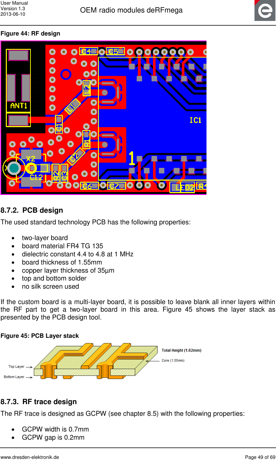
![User Manual Version 1.3 2013-06-10 OEM radio modules deRFmega www.dresden-elektronik.de Page 48 of 69 8.7. Reference Design for deRFmega256-23M12 8.7.1. Overview A reference design allows for a fast design-in of radio modules. Following its recommendations the most RF issues become subsidiary. Even with less or no RF experience it will be possible to get an optimal RF performance of a custom design. This reference design description must be respected for the use of deRFmega256-23M12 in the United States and to fulfil the requirements of FCC regulations according to the ‘Transmitter Module Equipment Authorization Guide’ [10]. See chapter 14.1 for further notes of FCC compliance. If the reference design will be integrated into a custom design, it will fulfil the FCC requirements too. The radio module deRFmega256-23M12 was measured and certified on the reference design board named RaspBee (see Figure 43). Further information on this device can be found in chapter 16. All following design descriptions are based on RaspBee. Figure 43: Reference design board (RaspBee) The design guide allows it to create a base board according to the reference board PCB properties. To fulfil the above-mentioned FCC requirements, the RF area of a custom PCB must have the same (design) properties. Any deviation from the reference design will result in a loss of FCC certification of the radio module and the custom design, unless the individual design will be certified again. However re-certification is possible and may be performed as Permissive Change Class II [11]. A partial re-measurement of RF properties is necessary. Note: Please get in contact with us to advise you for a custom FCC certified design. If necessary we will also provide RF part design data.. This may require signing a Non-Disclosure Agreement. The important area of the reference design is the RF part shown in Figure 44. One RF-OUT pad of the radio module is connected to the chip-antenna and the other RF-OUT pad is connected to a coaxial connector or an optional wire-antenna. It is also permitted to use only one of the both RF outputs, if needed. In this case terminate the unused port with 50ohms to ground.](https://usermanual.wiki/dresden-elektronik-ingenieurtechnik/MEGA23M12.15-MEGA23M12-User-Manual/User-Guide-2047839-Page-48.png)
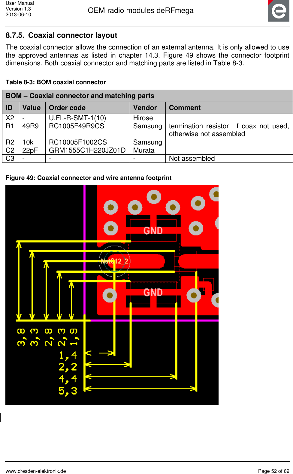
![User Manual Version 1.3 2013-06-10 OEM radio modules deRFmega www.dresden-elektronik.de Page 51 of 69 8.7.4. Chip-antenna The used chip-antenna is optimized for being placed at the PCB edge. Its footprint dimensions are shown in Figure 48. Further details of the used antenna can be found in the manufacturer’s datasheets [12]. The used antenna and all matching parts are listed in Table 8-2. Table 8-2: BOM chip antenna BOM – Chip antenna and matching parts ID Value Order code Vendor Comment ANT1 - 2450AT43B100 Johanson Technology C1 - - - Not assembled C13 22pF GRM1555C1H220JZ01D Murata L2 1.5nH HK10051N5S-T Taiyo Yuden Figure 48: Chip antenna footprint](https://usermanual.wiki/dresden-elektronik-ingenieurtechnik/MEGA23M12.15-MEGA23M12-User-Manual/User-Guide-2047839-Page-51.png)
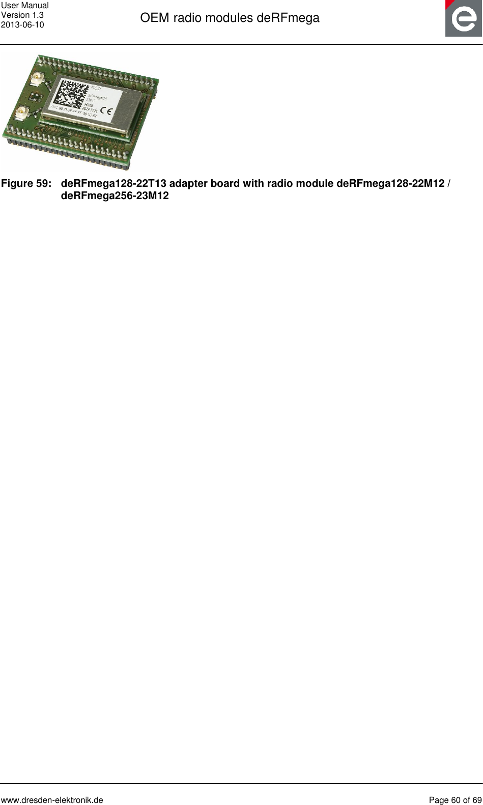
![User Manual Version 1.3 2013-06-10 OEM radio modules deRFmega www.dresden-elektronik.de Page 59 of 69 11. Programming The programming procedures are described in the documentation Fehler! Verweisquelle konnte nicht gefunden werden., which is online available on dresden elektronik webpage. It describes the update process of the radio module, the required software and hardware for programming via JTAG and the driver installation on different operating systems. The firmware programming of deRFmega256 radio modules is supported by Atmel Studio 6. 12. Pre-flashed firmware Actually, the radio modules will be delivered without pre-flashed firmware. 13. Adapter boards dresden elektronik offers these radio modules already soldered on suitable adapter boards. These boards can be plugged into dresden elektronik's development hardware platforms deRFbreakout Board, deRFnode or deRFgateway. For detailed information please refer to the datasheet [5], [6], [7] and [8] of the respective adapter board. Figure 57: deRFmega128-22T00 adapter board with radio module deRFmega128-22M00 / deRFmega256-23M00 Figure 58: deRFmega128-22T02 adapter board with radio module deRFmega128-22M10 / deRFmega256-23M10](https://usermanual.wiki/dresden-elektronik-ingenieurtechnik/MEGA23M12.15-MEGA23M12-User-Manual/User-Guide-2047839-Page-59.png)
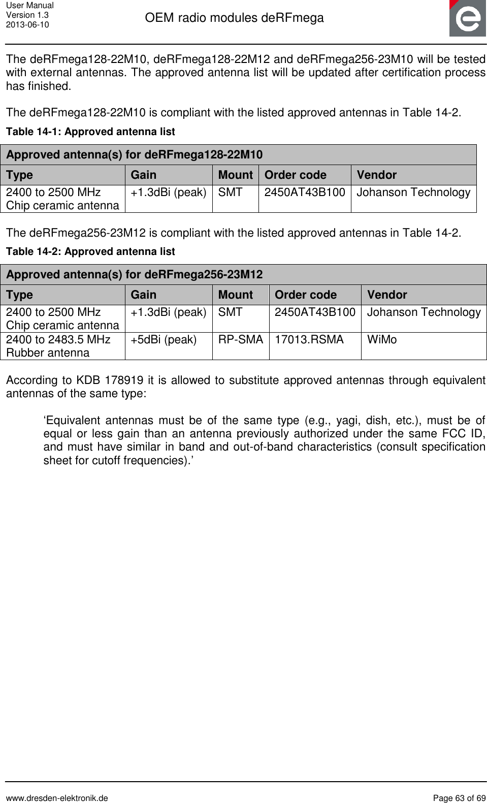
![User Manual Version 1.3 2013-06-10 OEM radio modules deRFmega www.dresden-elektronik.de Page 62 of 69 Modifications not expressly approved by this company could void the user's authority to operate this equipment (FCC section 15.21). This equipment has been tested and found to comply with the limits for a Class A digital device, pursuant to Part 15 of the FCC Rules. These limits are designed to provide reasonable protection against harmful interference when the equipment is operated in a commercial environment. This equipment generates, uses, and can radiate radio frequency energy and, if not installed and used in accordance with the instruction manual, may cause harmful interference to radio communications. Operation of this equipment in a residential area is likely to cause harmful interference in which case the user will be required to correct the interference at their own expense (FCC section 15.105). According to KDB 996369 the radio module deRFmega256-23M12 can only be used with a host antenna circuit trace layout design in strict compliance with the OEM instructions provided in this user manual. 14.2. European Union (ETSI) The deRFmega128-22M00, deRFmega128-22M10, deRFmega128-22M12, deRFmega256-23M00, deRFmega256-23M10 and deRFmega256-23M12 are conform for use in European Union countries. If the deRFmega128-22M00, deRFmega128-22M10, deRFmega128-22M12, deRFmega256-23M00, deRFmega256-23M10 and deRFmega256-23M12 modules are incorporated into a product, the manufacturer must ensure compliance of the final product to the European harmonized EMC and low-voltage/safety standards. A Declaration of Conformity must be issued for each of these standards and kept on file as described in Annex II of the R&TTE Directive. The manufacturer must maintain a copy of the deRFmega128-22M00, deRFmega128-22M10, deRFmega128-22M12, deRFmega256-23M00, deRFmega256-23M10 and deRFmega256-23M12 modules documentation and ensure the final product does not exceed the specified power ratings, antenna specifications, and/or installation requirements as specified in the user manual. If any of these specifications are exceeded in the final product, a submission must be made to a notified body for compliance testing to all required standards. The CE marking must be affixed to a visible location on the OEM product. The CE mark shall consist of the initials "CE" taking the following form: If the CE marking is reduced or enlarged, the proportions must be respected. The CE marking must have a height of at least 5 mm except where this is not possible on account of the nature of the apparatus. The CE marking must be affixed visibly, legibly, and indelibly. More detailed information about CE marking requirements can be found in [9]. 14.3. Approved antennas The deRFmega128-22M00 and deRFmega256-23M00 has an integrated chip antenna. The design is fully compliant with all regulations. The certification process is pending for deRFmega256-23M00.](https://usermanual.wiki/dresden-elektronik-ingenieurtechnik/MEGA23M12.15-MEGA23M12-User-Manual/User-Guide-2047839-Page-62.png)
![User Manual Version 1.3 2013-06-10 OEM radio modules deRFmega www.dresden-elektronik.de Page 66 of 69 17. Packaging dimension Currently the radio modules are delivered as singular pieces with an appropriate ESD packaging. The delivery as Tape & Reel will be possible for larger amounts but is not yet available. Further information will be described in this section as Tape & Reel delivery becomes available. 18. Revision notes Actually, no design issues of the radio modules are known. All errata of the AVR MCU ATmega128RFA1 are described in the datasheet [1]. All errata of the AVR MCU ATmega256RFR2 are described in the datasheet [2].](https://usermanual.wiki/dresden-elektronik-ingenieurtechnik/MEGA23M12.15-MEGA23M12-User-Manual/User-Guide-2047839-Page-66.png)
![User Manual Version 1.3 2013-06-10 OEM radio modules deRFmega www.dresden-elektronik.de Page 67 of 69 19. References [1] ATmega128RFA1: 8-bit AVR Microcontroller with Low Power 2.4 GHz Transceiver for ZigBee and IEEE802.15.4; Datasheet, URL: http://www.atmel.com [2] ATmega256RFR2: 8-bit AVR Microcontroller with Low Power 2.4 GHz Transceiver for ZigBee and IEEE802.15.4; Datasheet, URL: http://www.atmel.com [3] AppCAD Version 3.0.2, RF & Microwave design software, Agilent Technologies; URL: http://www.hp.woodshot.com [4] User Manual Firmware Update; URL: http://www.dresden-elektronik.de/funktechnik/products/radio-modules/oem-derfmega/description/?L=0&eID=dam_frontend_push&docID=1917 [5] Datasheet adapter board 22T00 | 22T02, URL: http://www.dresden-elektronik.de/funktechnik/products/radio-modules/adapter-boards-oem-modules/description/?L=1%252Fproducts%252Fusb-radio-sticks%252Fderfusb-analyzer%252F%253FL%253D1&eID=dam_frontend_push&docID=1816 [6] Datasheet adapter board 22T13, URL: http://www.dresden-elektronik.de/funktechnik/products/radio-modules/adapter-boards-oem-modules/description/?L=1%252Fproducts%252Fusb-radio-sticks%252Fderfusb-analyzer%252F%253FL%253D1&eID=dam_frontend_push&docID=1818 [7] Datasheet adapter board 23T00 | 23T02, URL: http://www.dresden-elektronik.de/funktechnik/products/radio-modules/adapter-boards-oem-modules/description/?L=1&eID=dam_frontend_push&docID=1859 [8] Datasheet adapter board 23T13, URL: http://www.dresden-elektronik.de/funktechnik/products/radio-modules/adapter-boards-oem-modules/description/?L=1&eID=dam_frontend_push&docID=1861 [9] Directive 1999/5/EC, European Parliament and the Council, 9 March 1999, section 12 [10] Transmitter Module Equipment Authorization Guide; 996369 D01 Module Certification Guide; FCC OET; URL: https://apps.fcc.gov/oetcf/kdb/forms/FTSSearchResultPage.cfm?id=44637&switch=P [11] Permissive Change Policy; 178919 D01 Permissive Change Policy); FCC OET; URL: https://apps.fcc.gov/oetcf/kdb/forms/FTSSearchResultPage.cfm?id=33013&switch=P [12] 2.4GHz Chip-Antenna 2450AT43B100 by JOHANSON TECHNOLOGY; Datasheet; URL: http://www.johansontechnology.com/datasheets/antennas/2450AT43B100.pdf](https://usermanual.wiki/dresden-elektronik-ingenieurtechnik/MEGA23M12.15-MEGA23M12-User-Manual/User-Guide-2047839-Page-67.png)