Topcon TIWIBLE TiWi-BLE User Manual Topcon Rev2
Topcon Corporation TiWi-BLE Topcon Rev2
UserManual.wiki
>
Topcon
>
TIWIBLE User Manual
Users Manual Rev 2
Navigation menu
Upload a User Manual
Namespaces
Wiki Guide
HTML
PDF
Info
Views
User Manual
Discussion / Help
Navigation
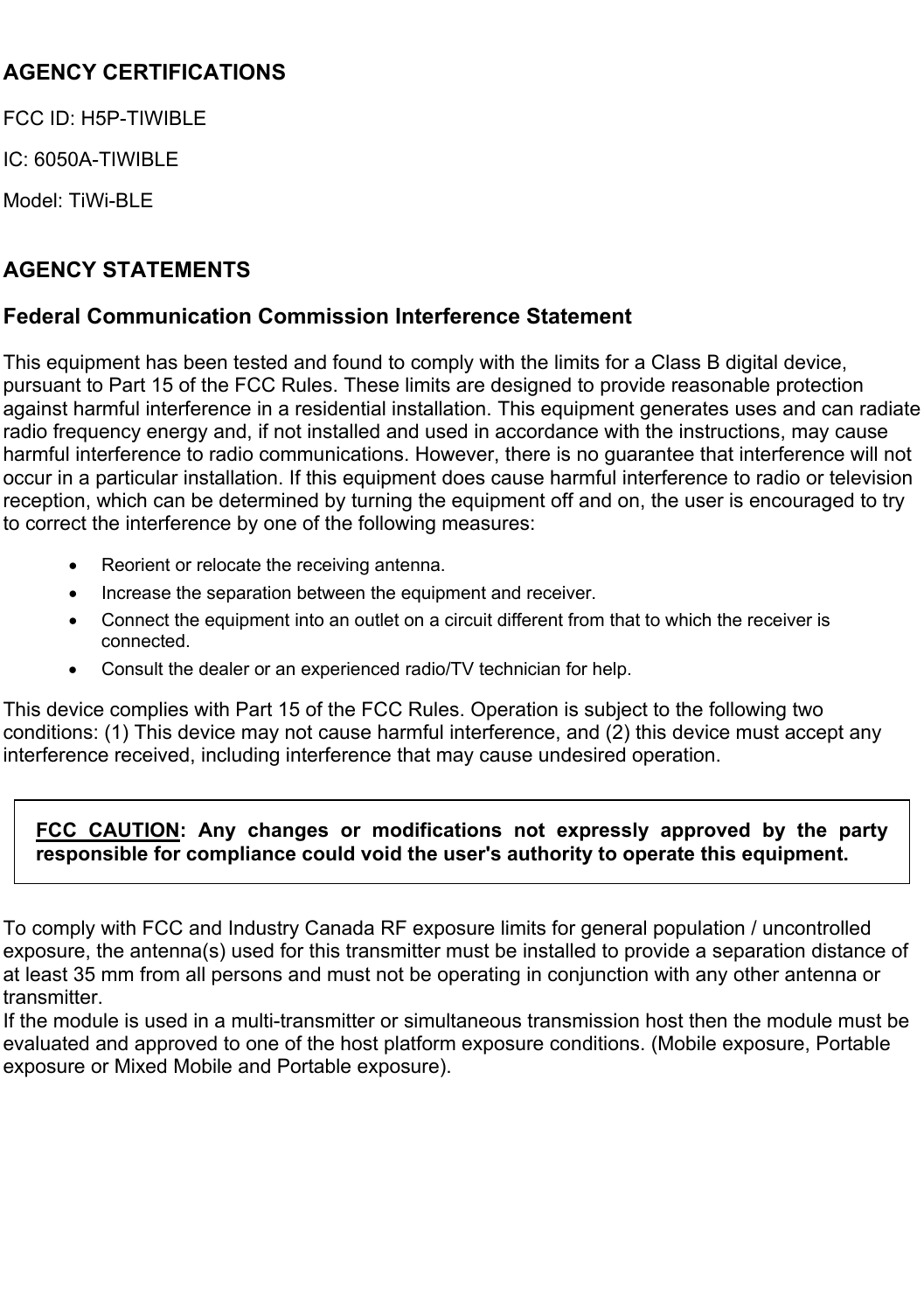
![General Characteristics Parameter Min Typ Max Unit WLAN RF frequency range 2412 2472 MHz WLAN RF data rate 1 802.11 b/g/n rates supported 65 MbpsTable 3 General Characteristics Power Consumption - WLAN Parameter Test Conditions Min Typ Max Unit CCK (802.11b) TX Current 2437 MHz, VBAT =3.6V, Tamb=+25°C Po=20dBm, 11 Mbps CCK L=1200 bytes, tdelay (idle)=4 S - 280 - mA OFDM (802.11g) TX Current 2437 MHz, VBAT =3.6V, Tamb=+25°C Po=14.5 dBm, 54 Mbps OFDM L=1200 bytes, tdelay (idle)=4S - 185 - mA OFDM (802.11n) TX Current 2437 MHz, VBAT =3.6V, Tamb=+25°C Po=12.5dBm, 65 Mbps OFDM L=1200 bytes, tdelay (idle)=4S - 165 - mA CCK (802.11b) RX Current - 100 - mA OFDM (802.11g) RX Current - 100 - mA OFDM (802.11n) RX Current - 100 - mA Dynamic Mode [1] - <1.2 - mA [1] Total Current from VBAT for reception of Beacons with DTIM=1 TBTT=100 mS, Beacon duration 1.6ms, 1 Mbps beacon reception in Listen Mode. Table 4 WLAN Power Consumption](https://usermanual.wiki/Topcon/TIWIBLE/User-Guide-2835586-Page-3.png)
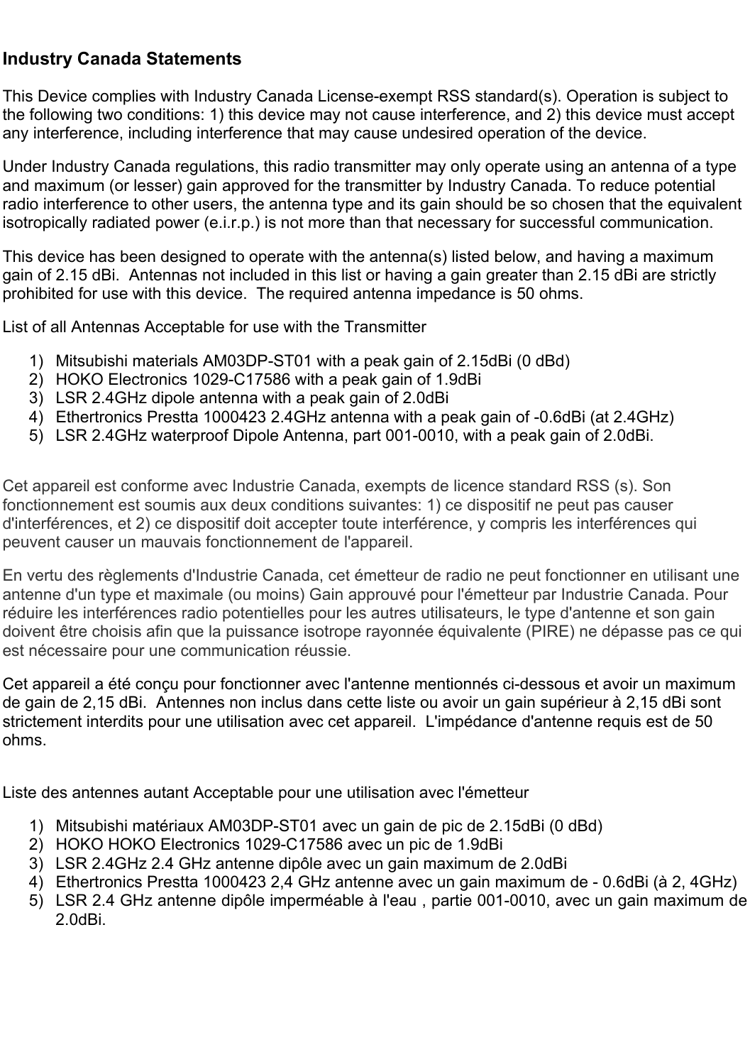
![WLAN Receiver Characteristics (TA=25°C, VBAT=3.6 V) [1] Parameter Test Conditions Min Typ Max Unit 1 Mbps CCK (802.11b) RX Sensitivity 8% PER - -97 - dBm 11 Mbps CCK (802.11b) RX Sensitivity 8% PER - -89 - dBm 9 Mbps OFDM (802.11g) RX Sensitivity 10% PER - -90 - dBm 54 Mbps OFDM (802.11g) RX Sensitivity 10% PER - -76 - dBm 6.5 Mbps OFDM (802.11n) RX Sensitivity 10% PER - -91 - dBm 65 Mbps OFDM (802.11n) RX Sensitivity 10% PER - -73 -- dBm 11 Mbps CCK (802.11b) RX Overload Level 8% PER - - -10 dBm 6 Mbps OFDM (802.11g) RX Overload Level 10% PER - - -20 dBm 54 Mbps OFDM (802.11g) RX Overload Level. 10% PER - - -20 dBm 65 Mbps OFDM (802.11n) RX Overload Level 10% PER - - -20 dBm [1] Up to 2 dB degradation at Channel 13 for 11g/n modes and up to 2 dB degradation at Channel 14 for 11b/g/n modes. Table 7 WLAN Receiver RF Characteristics](https://usermanual.wiki/Topcon/TIWIBLE/User-Guide-2835586-Page-5.png)
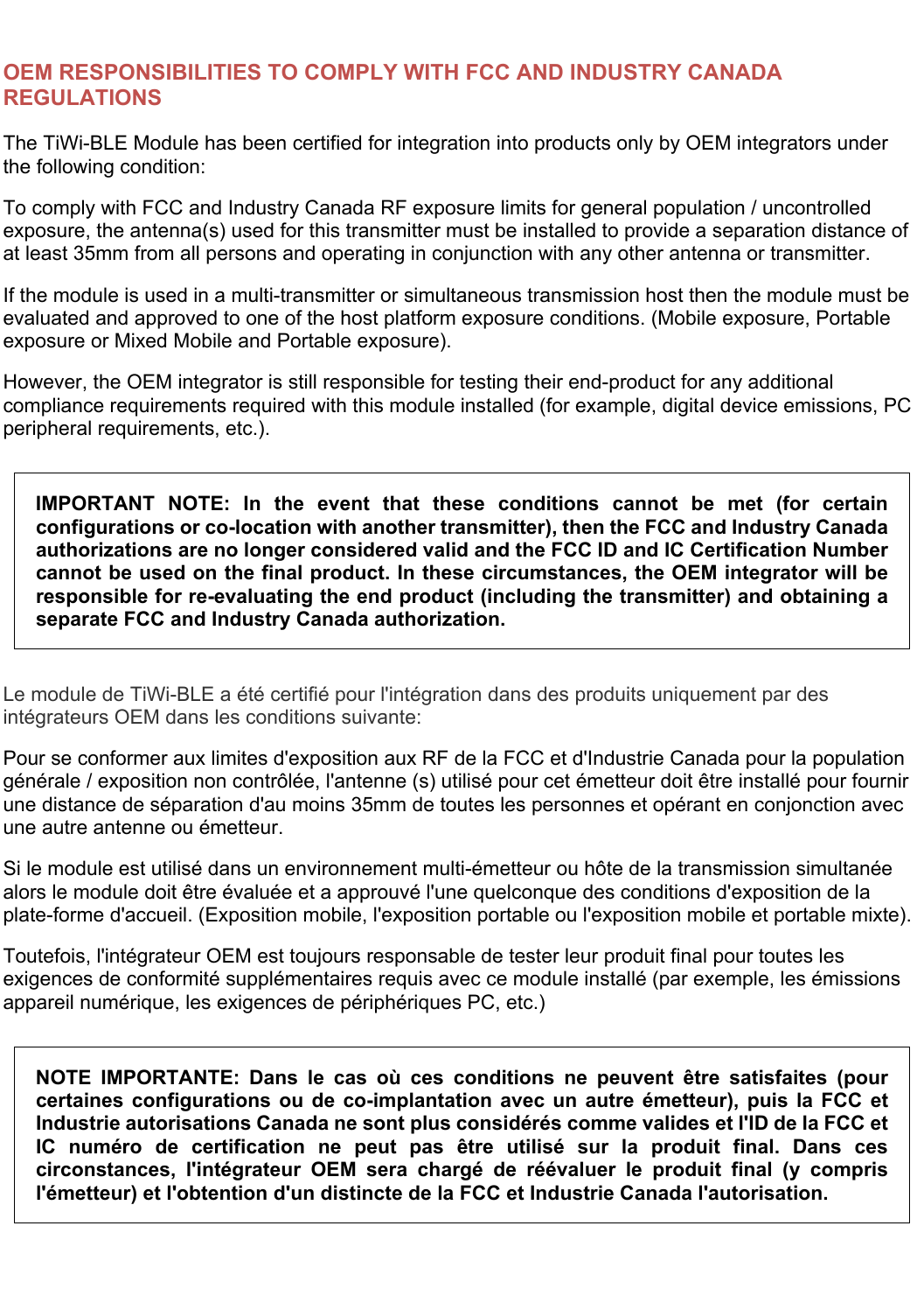
![SLOW (32 KHZ) CLOCK SOURCE REQUIREMENTS The slow clock is always supplied from an external source. It is input on the SLOW_CLK pin, and can be a digital signal in the range of VIO only. For slow clock frequency and accuracy refer to Table 8. The external slow clock must be stable before the system exits from shut down mode. Parameter [1] Condition Symbol Min Typ Max Unit Input slow clock frequency 32768 Hz Input slow clock accuracy WLAN, BT +/-250 ppm Input transition time Tr/Tf – 10% to 90% Tr/Tf 100 ns Frequency input duty cycle 30 50 70 % Input voltage limits Square wave, DC coupled VIH 0.65 x VDDS VDDS Vpeak VIL 0 0.35 x VDDS Input impedance 1 MW Input capacitance 5 pF Rise and fall time 100 ns Phase noise 1 kHz -125 dBc/Hz [1] Slow clock is a fail safe input Table 8 Slow Clock Source Requirements](https://usermanual.wiki/Topcon/TIWIBLE/User-Guide-2835586-Page-9.png)