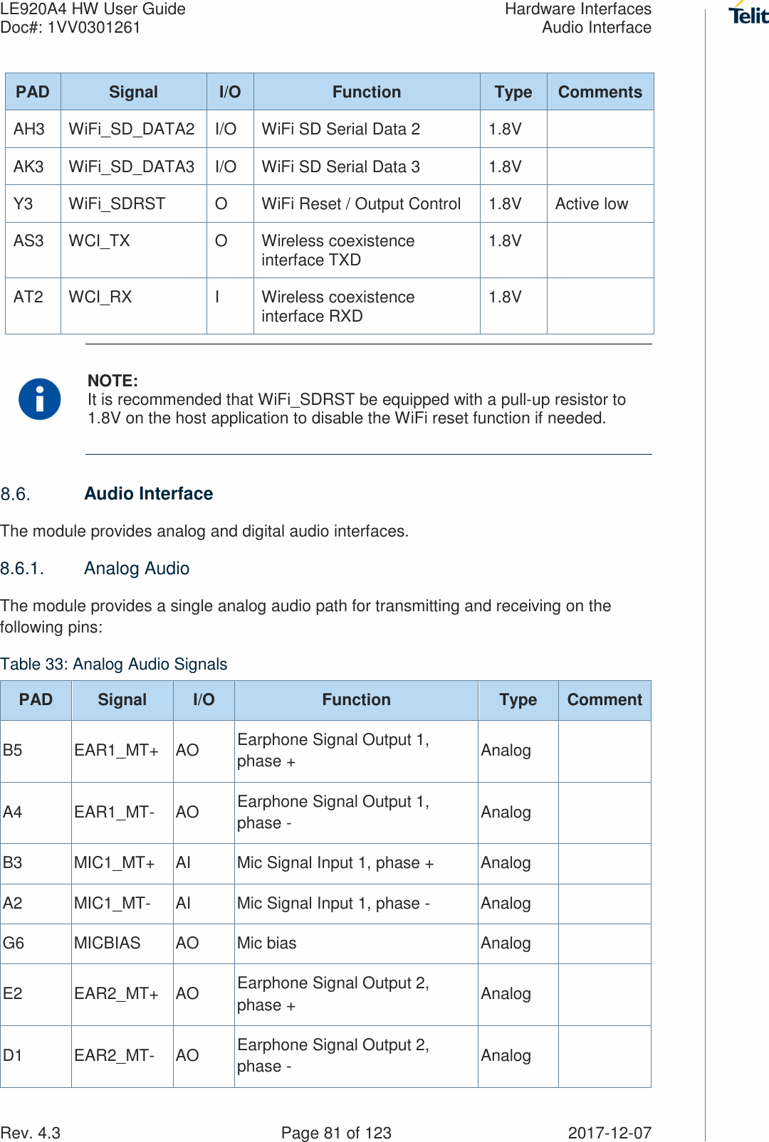
Telit Communications S p A LE920A4NA Wireless Module User Manual 1vv0301261 LE920A4 HW User Guide r4 3
Telit Communications S.p.A. Wireless Module 1vv0301261 LE920A4 HW User Guide r4 3
UserManual.wiki
>
Telit Communications S p A
>
LE920A4NA User Manual
>
User manual
Contents
1.
User Manual
2.
User manual
User manual
Navigation menu
Upload a User Manual
Namespaces
Wiki Guide
HTML
PDF
Info
Views
User Manual
Discussion / Help
Navigation
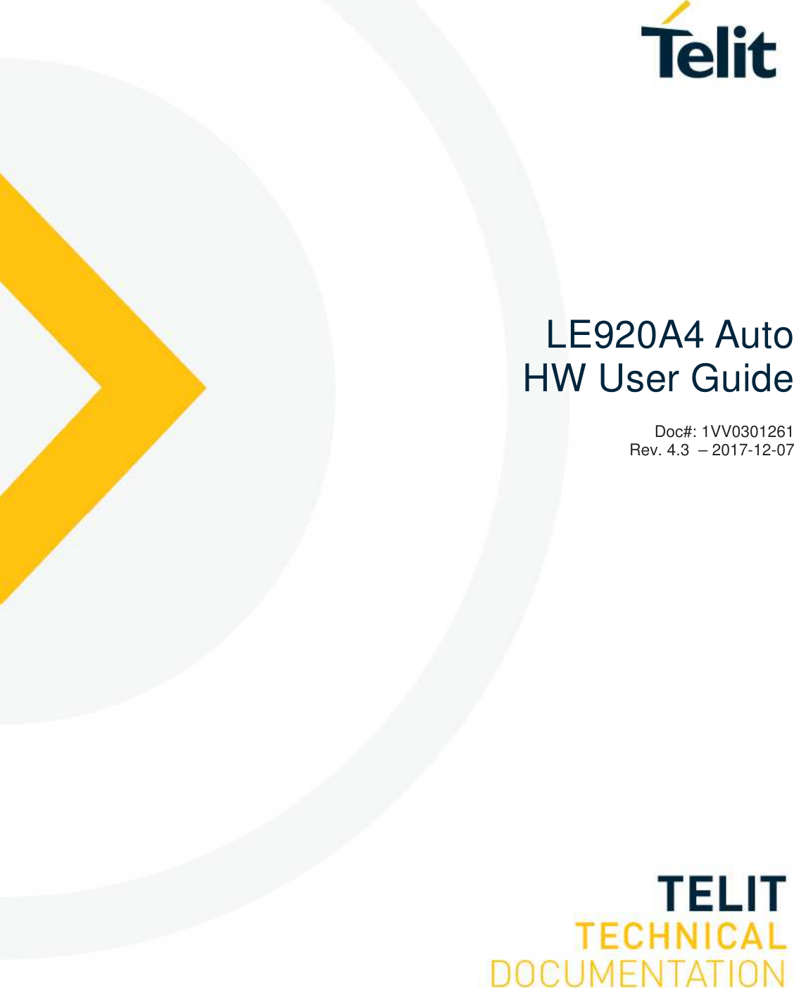
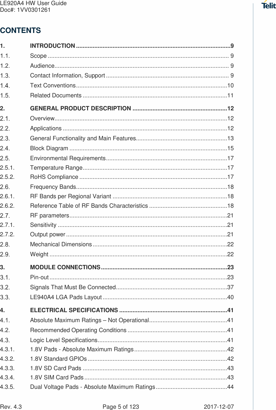
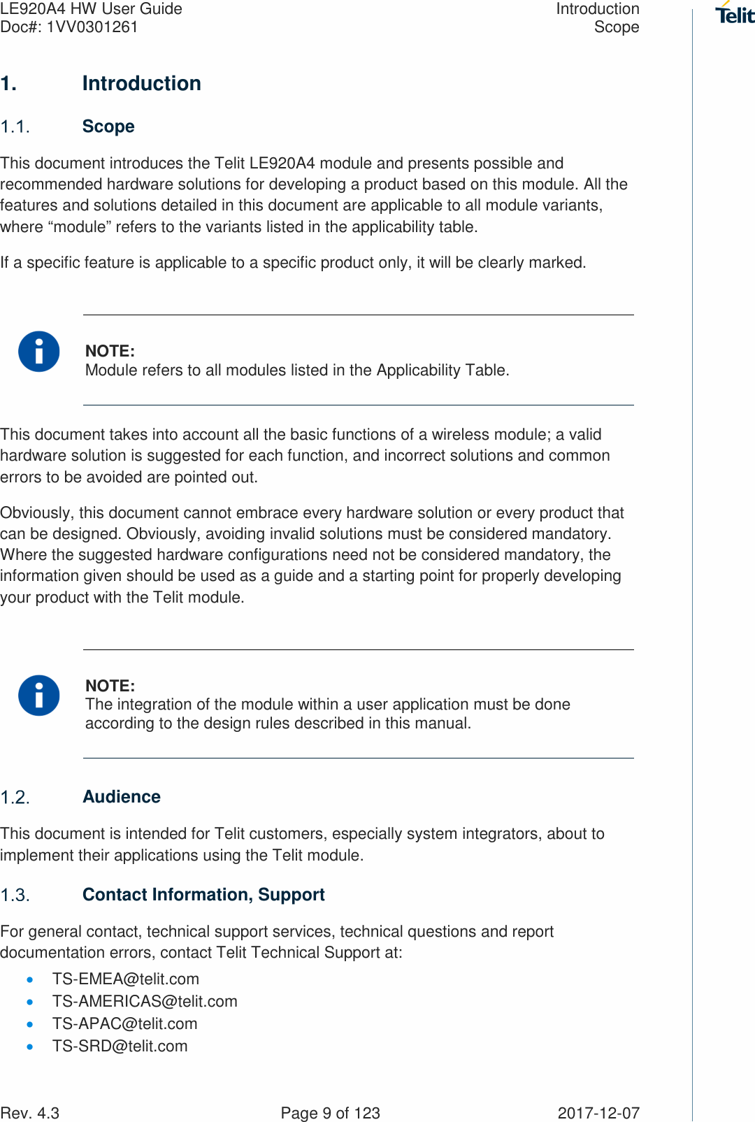
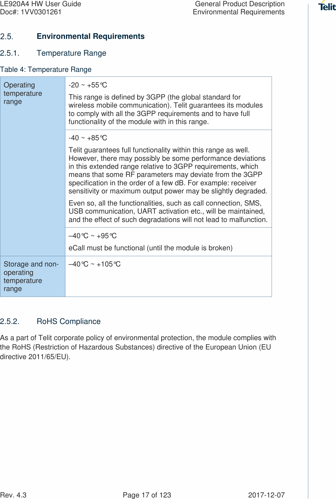
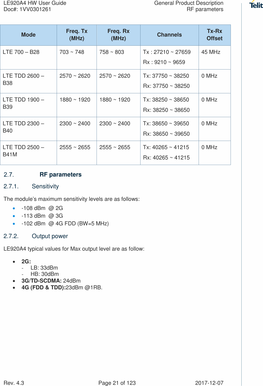


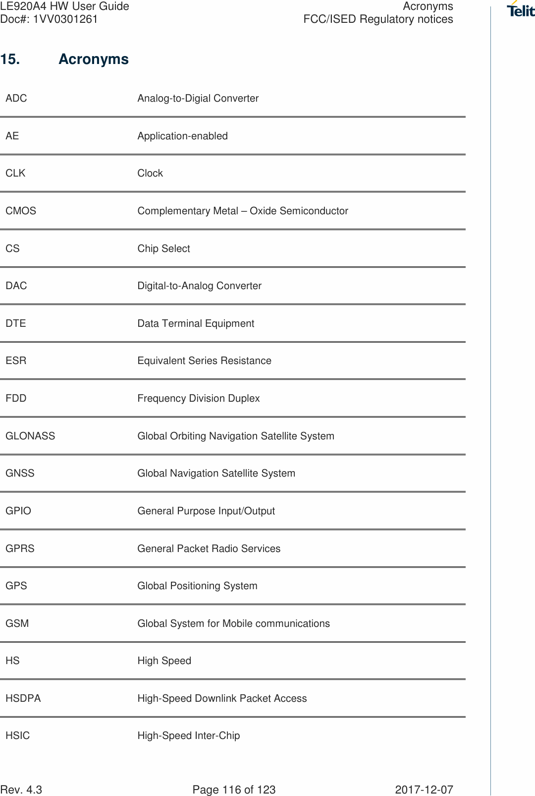
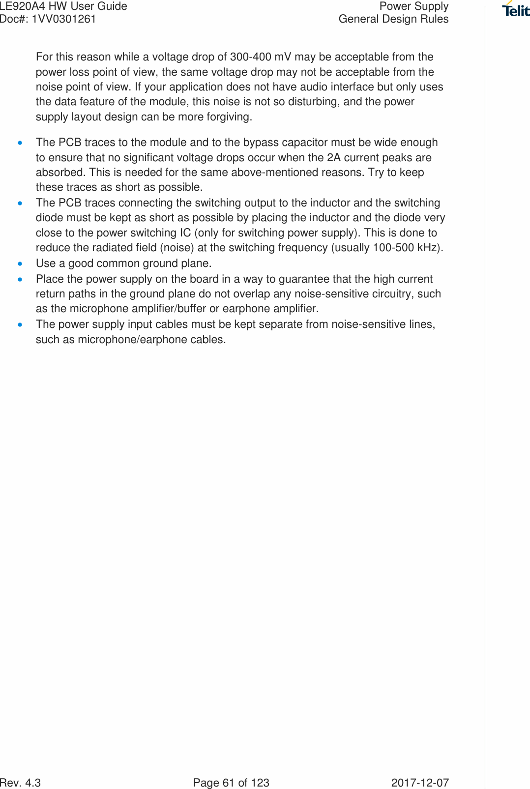
![LE920A4 HW User Guide Electrical Specifications Doc#: 1VV0301261 Absolute Maximum Ratings – Not Operational Rev. 4.3 Page 41 of 123 2017-12-07 4. Electrical Specifications Absolute Maximum Ratings – Not Operational WARNING: A deviation from the value ranges listed below may harm the module. Table 9: Absolute Maximum Ratings – Not Operational Symbol Parameter Min Max Unit VBATT Battery supply voltage on VBATT pin -0.5 +6.0 [V] VBATT TRANSIENT Transient voltage on pin VBATT (< 10 ms) -0.5 +7.0 [V] VBATT_PA Battery supply voltage on VBATT_PA pin -0.3 +6.0 [V] Recommended Operating Conditions Table 10: Recommended Operating Conditions Symbol Parameter Min Typ Max Unit Tamb Ambient temperature -40 +25 +85 [°C] VBATT Battery supply voltage on VBATT pin 3.4 3.8 4.2 [V] VBATT_PA Battery supply voltage on VBATT_PA pin 3.4 3.8 4.2 [V] IBATT_PA + IBATT Peak current to be used to dimension decoupling capacitors on VBATT_PA pin - 80 2000 [mA] Logic Level Specifications Unless otherwise specified, all the interface circuits of the module are 1.8V CMOS logic. Only few specific interfaces (such as USIM and SD Card) are capable of dual voltage I/O.](https://usermanual.wiki/Telit-Communications-S-p-A/LE920A4NA.User-manual/User-Guide-3744131-Page-41.png)
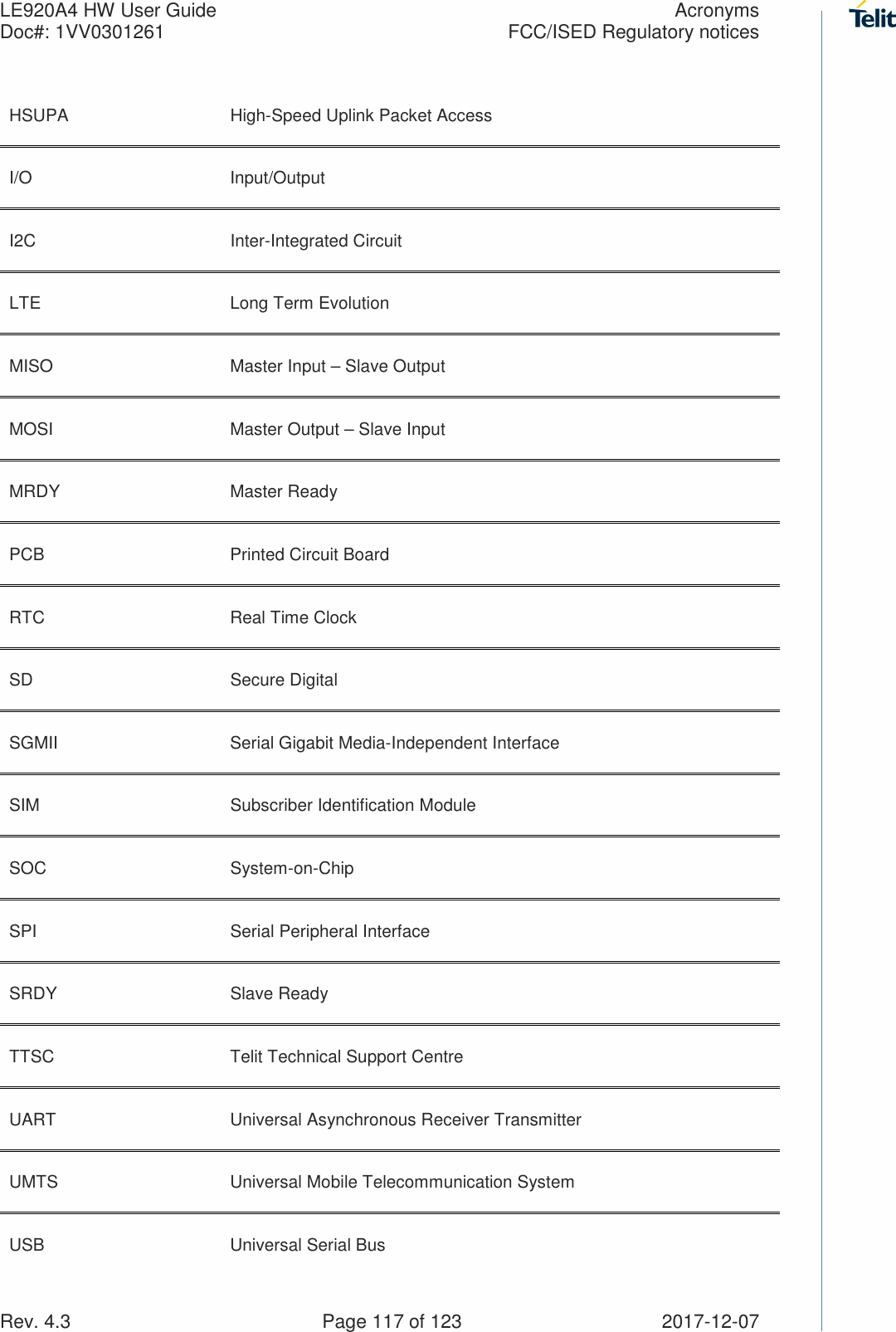
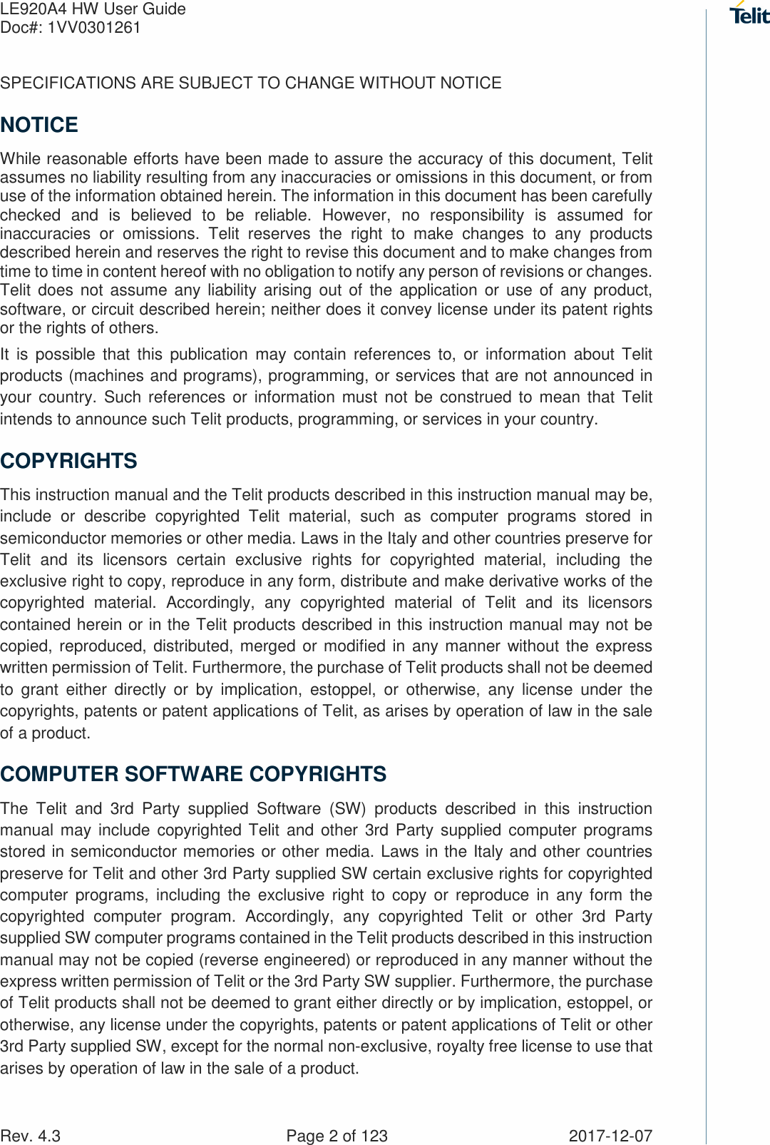
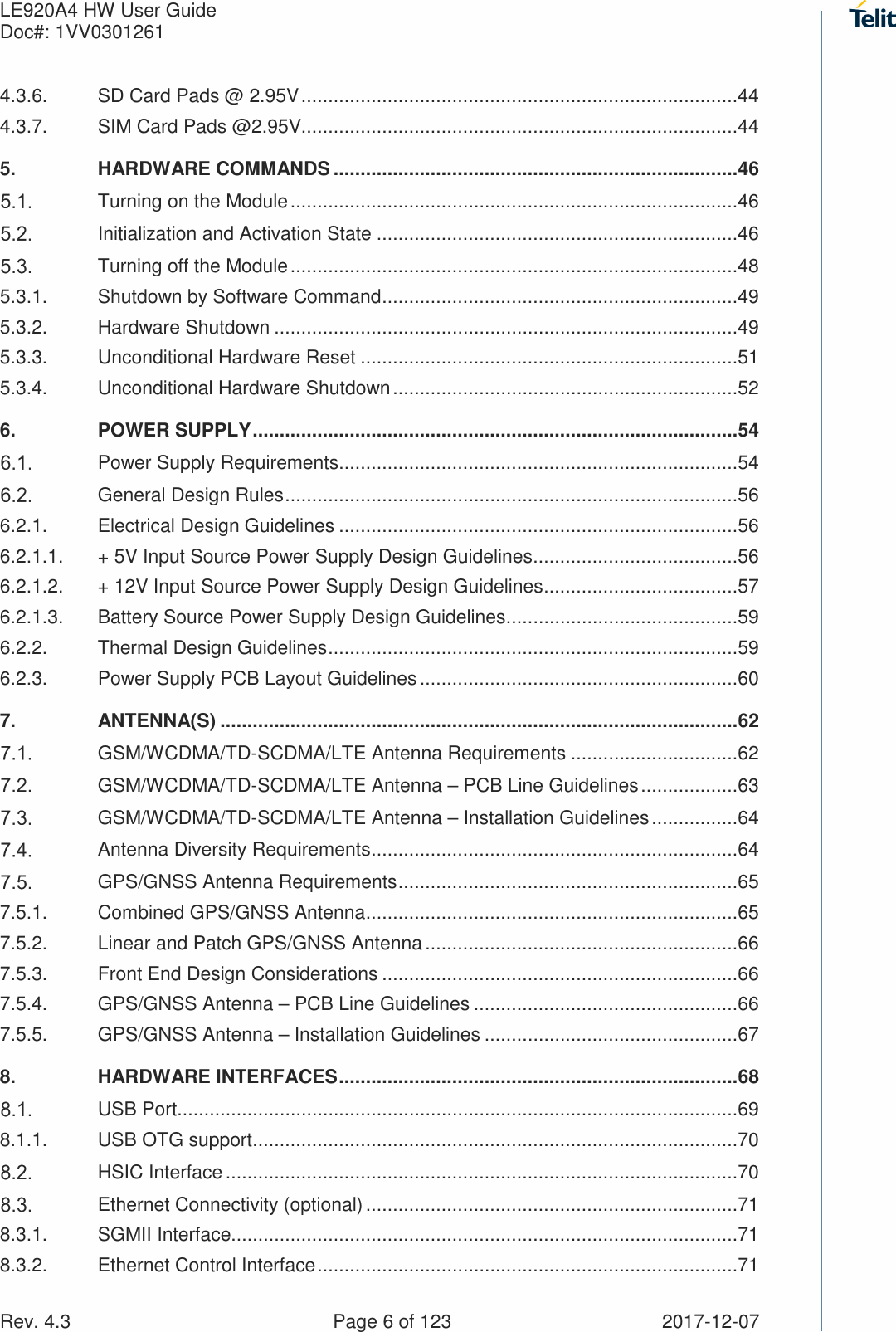
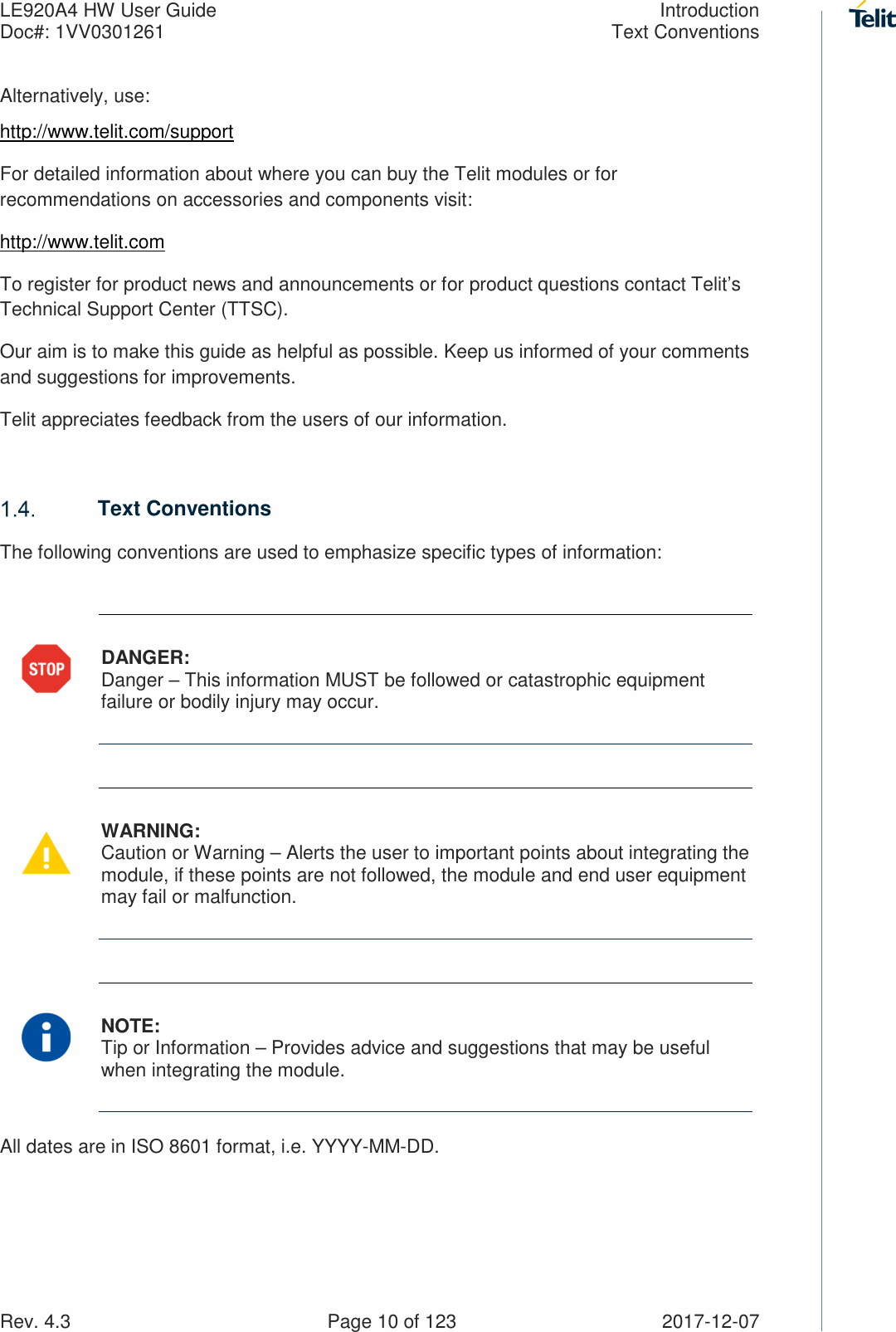
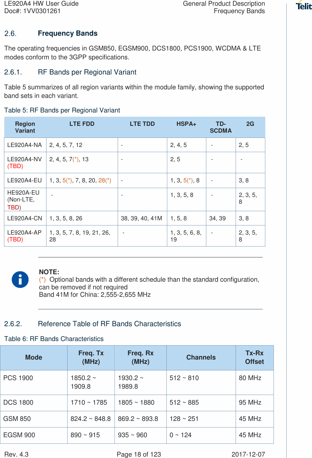
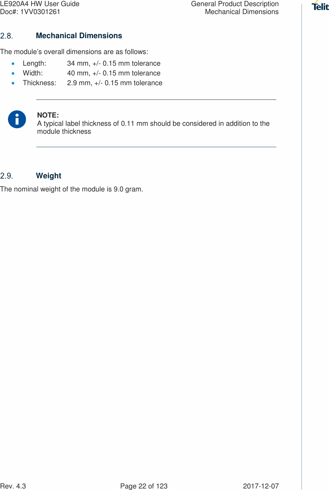
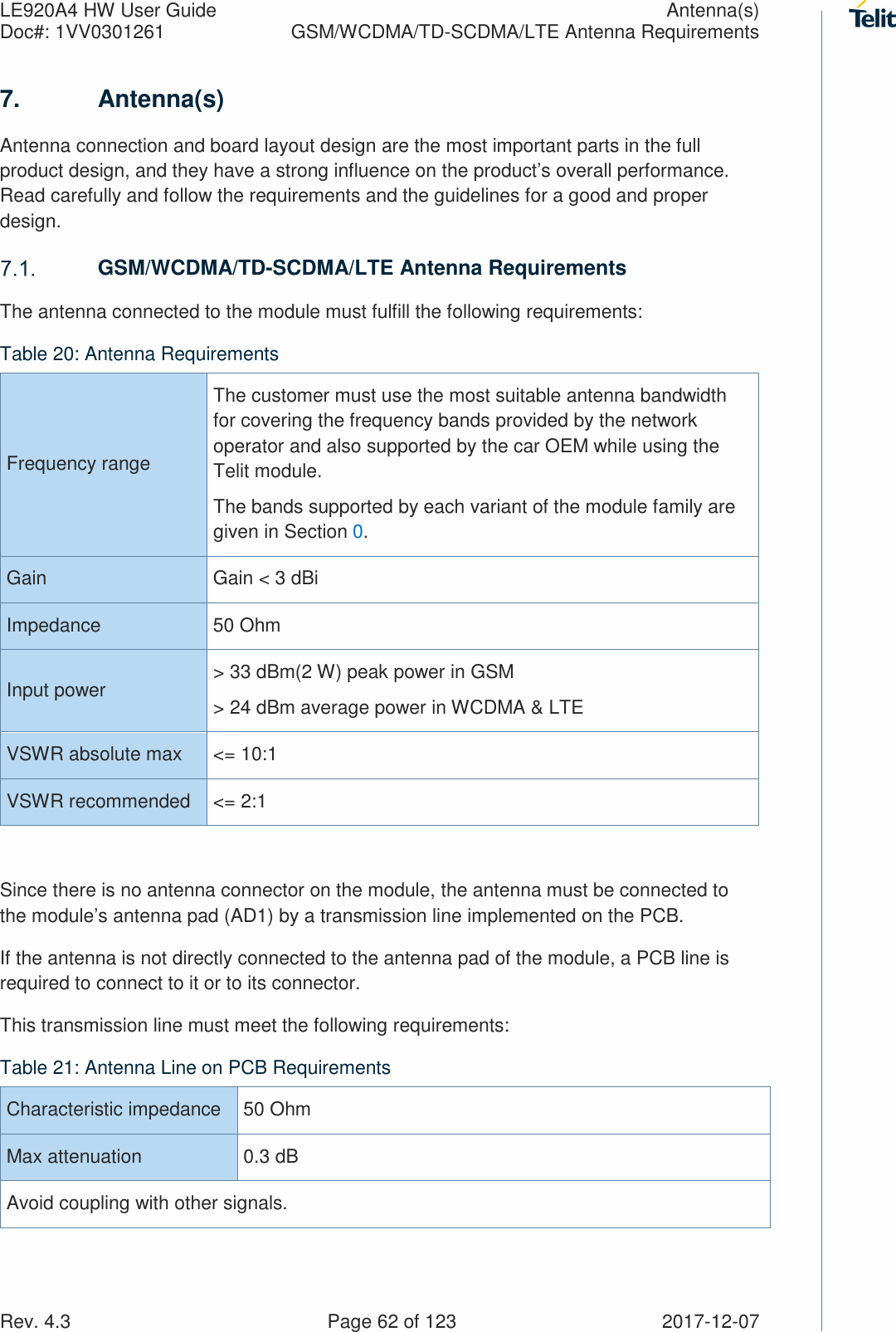
![LE920A4 HW User Guide Electrical Specifications Doc#: 1VV0301261 Logic Level Specifications Rev. 4.3 Page 42 of 123 2017-12-07 The following tables show the logic level specifications used in the module’s interface circuits. The data specified in the tables below is valid throughout all drive strengths and the entire temperature ranges. NOTE: Do not connect the module’s digital logic signals directly to the OEM’s digital logic signals with a level higher than 2.7V for 1.8V CMOS signals. 4.3.1. 1.8V Pads - Absolute Maximum Ratings Table 11: Absolute Maximum Ratings - Not Functional Parameter Min Max Input level on any digital pin when on -0.3V +2.16V Input voltage on analog pins when on -0.3V +2.16 V 4.3.2. 1.8V Standard GPIOs Table 12: Operating Range – Interface Levels (1.8V CMOS) Pad Parameter Min Max Unit Comment VIH Input high level 1.25V -- [V] VIL Input low level -- 0.6V [V] VOH Output high level 1.4V -- [V] VOL Output low level -- 0.45V [V] IIL Low-level input leakage current -1 -- [uA] No pull-up IIH High-level input leakage current -- +1 [uA] No pull-down RPU Pull-up resistance 30 390 [kΩ] See Note RPD Pull-down resistance 30 390 [kΩ] See Note Ci Input capacitance -- 5 [pF]](https://usermanual.wiki/Telit-Communications-S-p-A/LE920A4NA.User-manual/User-Guide-3744131-Page-42.png)
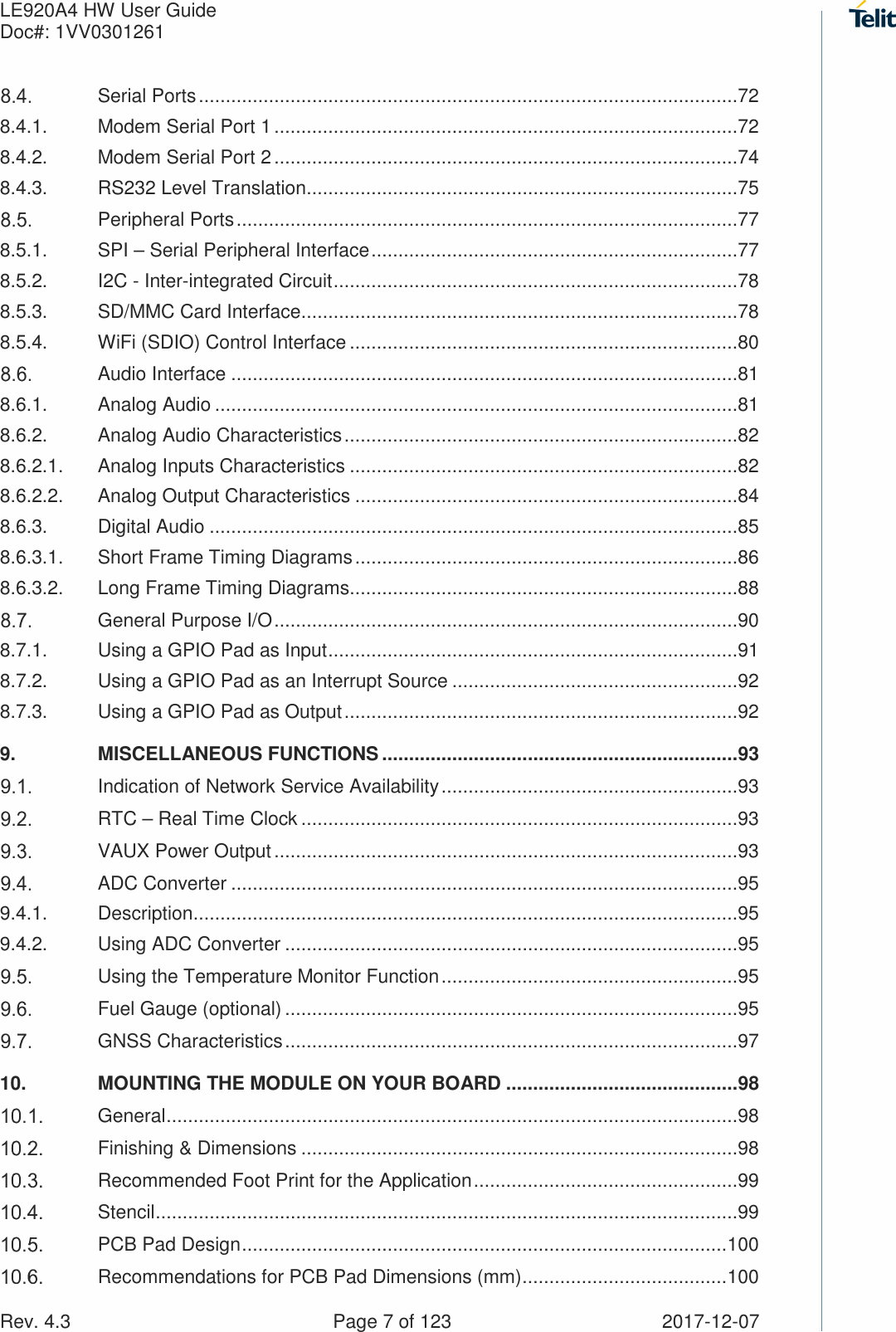
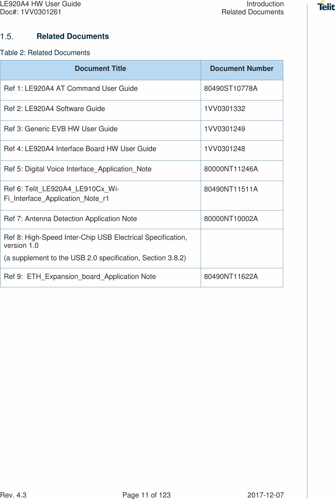
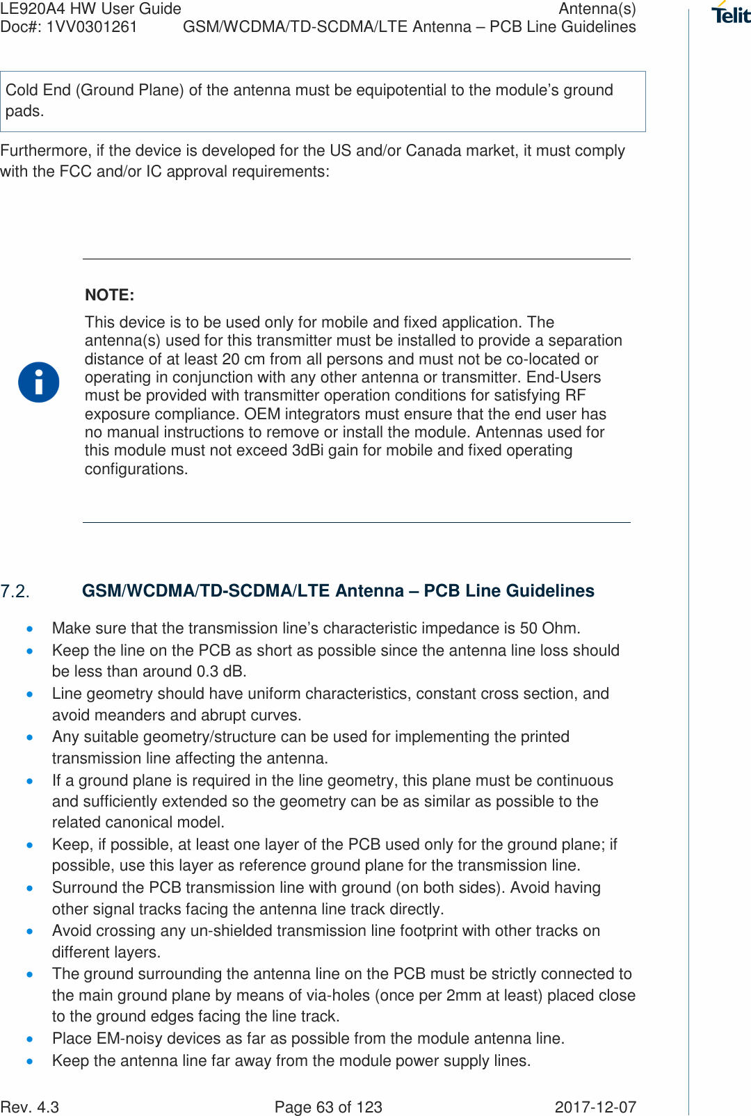
![LE920A4 HW User Guide Electrical Specifications Doc#: 1VV0301261 Logic Level Specifications Rev. 4.3 Page 43 of 123 2017-12-07 NOTE: Pull-up and Pull-down resistance of GPIO5 is different from those mentioned above. GPIO5 pull resistance is specified as 10KΩ to 50KΩ. 4.3.3. 1.8V SD Card Pads Table 13: Operating Range – SD Card Pads Working at 1.8V Pad Parameter Min Max Unit Comment VIH Input high level 1.27V 2V [V] VIL Input low level -0.3V 0.58V [V] VOH Output high level 1.4V -- [V] VOL Output low level 0 0.45V [V] IIL Low-level input leakage current -2 - [uA] No pull-up IIH High-level input leakage current - 2 [uA] No pull-down RPU Pull-up resistance 10 100 [kΩ] RPD Pull-down resistance 10 100 [kΩ] Ci Input capacitance 5 [pF] 4.3.4. 1.8V SIM Card Pads Table 14: Operating Range – SIM Pads Working at 1.8V Pad Parameter Min Max Unit Comment VIH Input high level 1.35V 2V [V] VIL Input low level -0.3V 0.43V [V] VOH Output high level 1.35V 1.875V [V] VOL Output low level 0V 0.4V [V] IIL Low-level input leakage current -2 - [uA] No pull-up IIH High-level input leakage current - 2 [uA] No pull-down](https://usermanual.wiki/Telit-Communications-S-p-A/LE920A4NA.User-manual/User-Guide-3744131-Page-43.png)
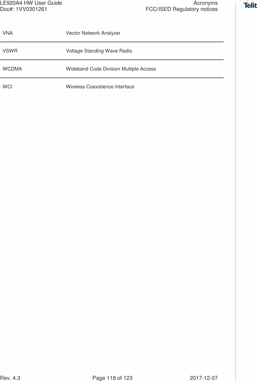
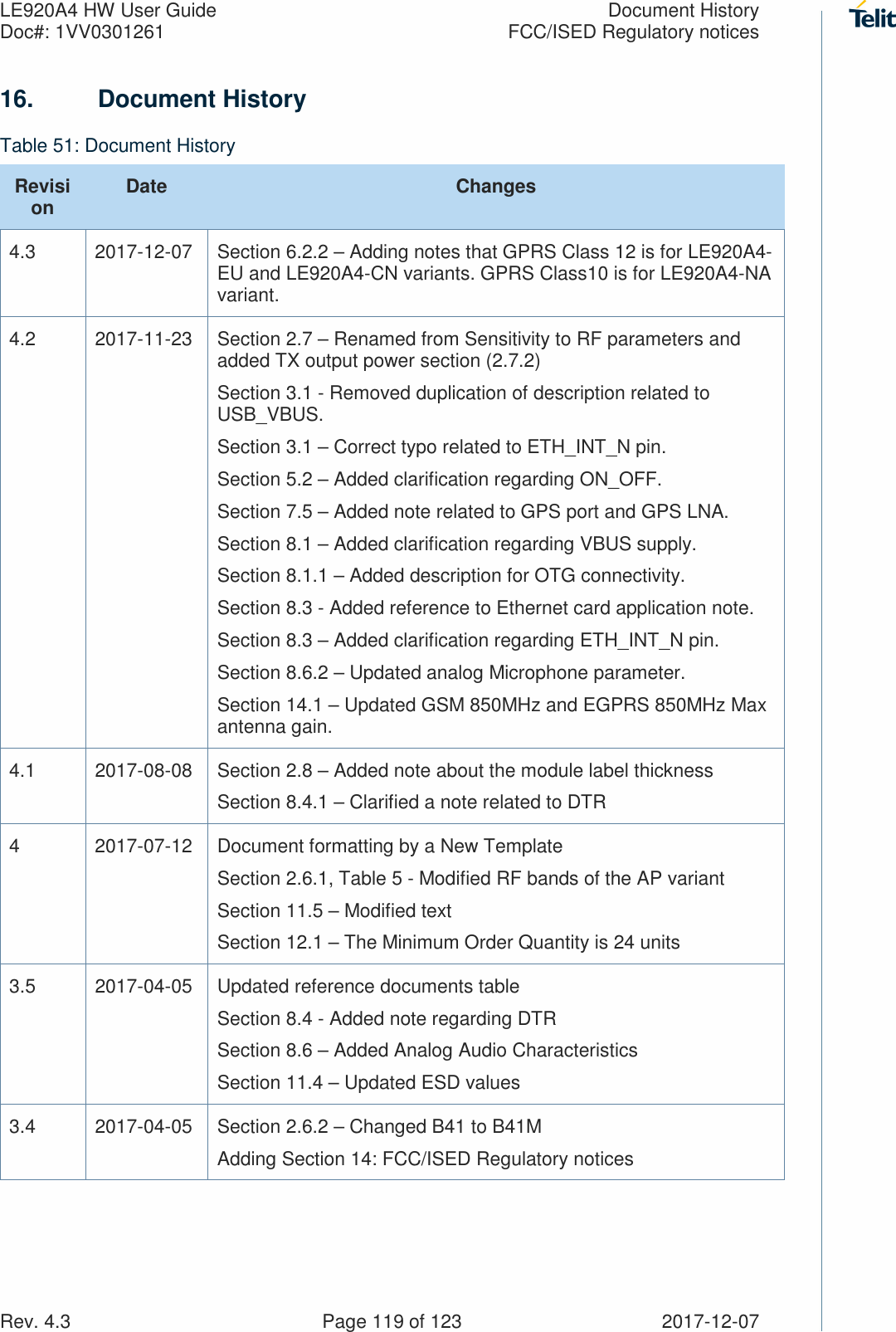
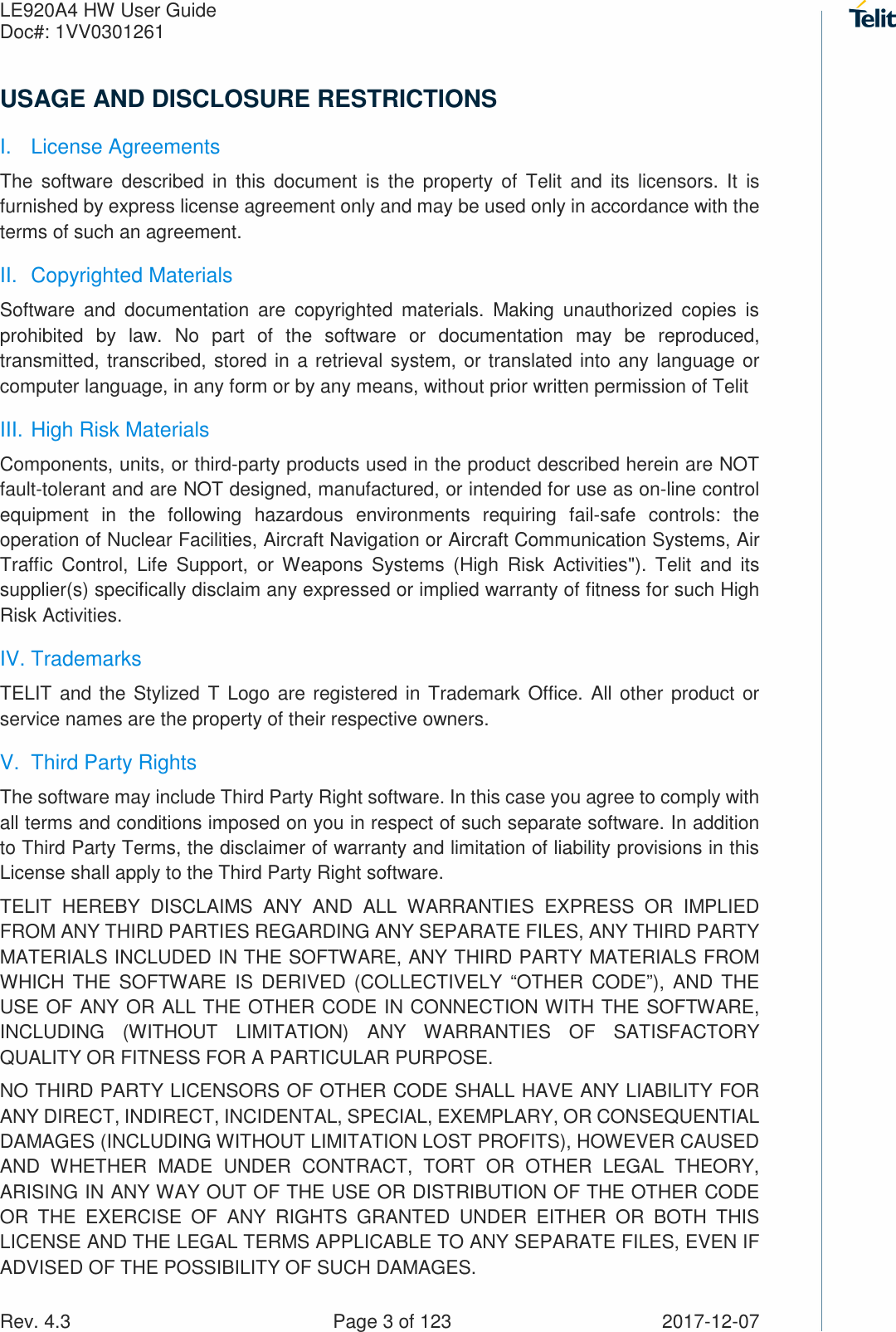
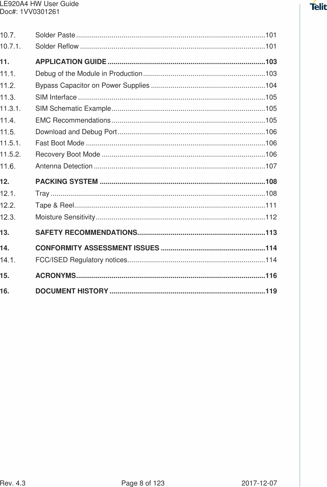
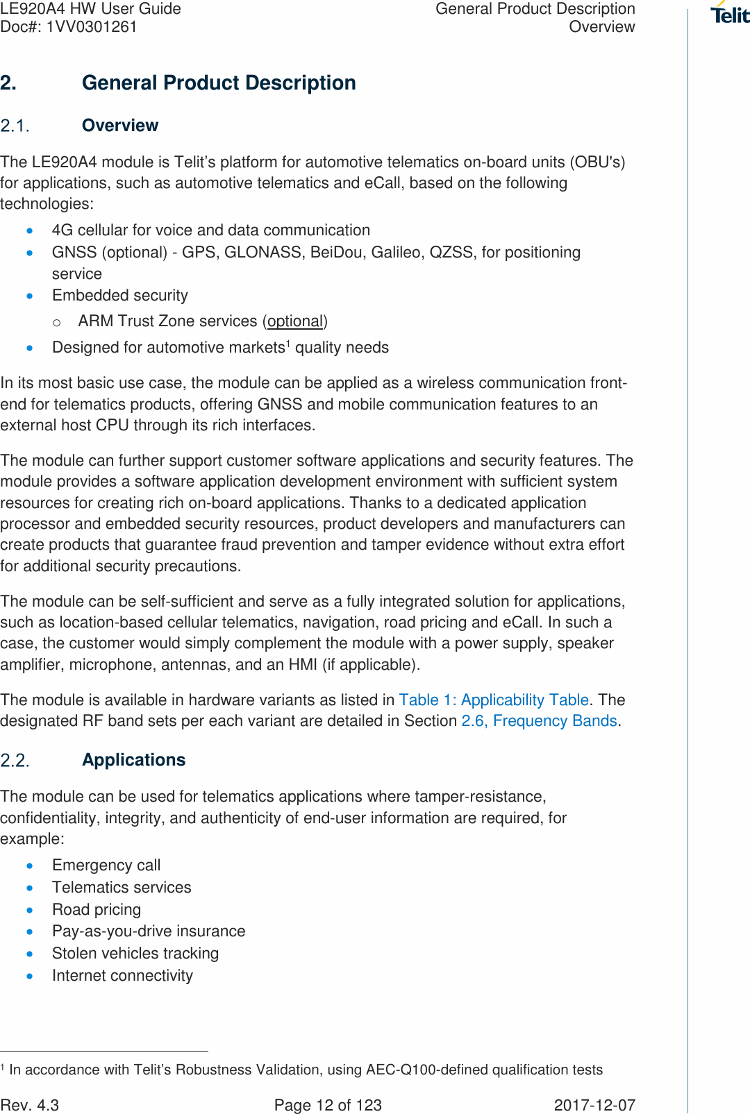
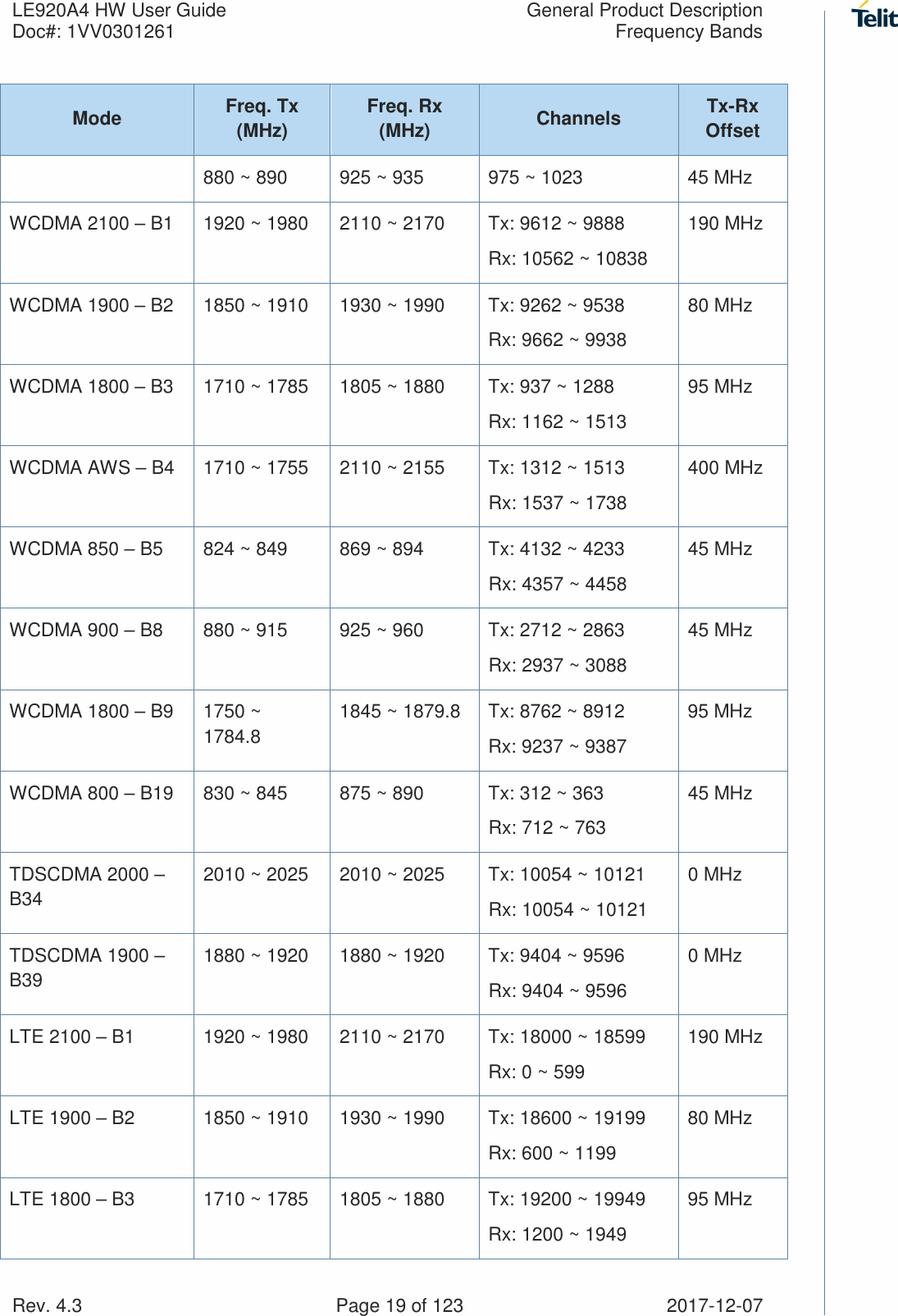
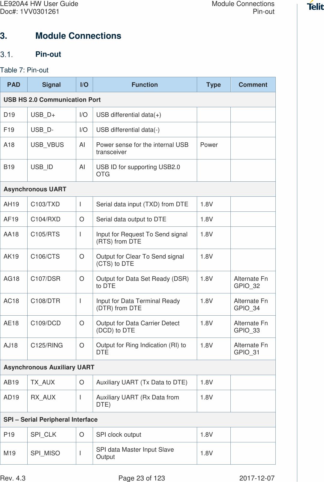
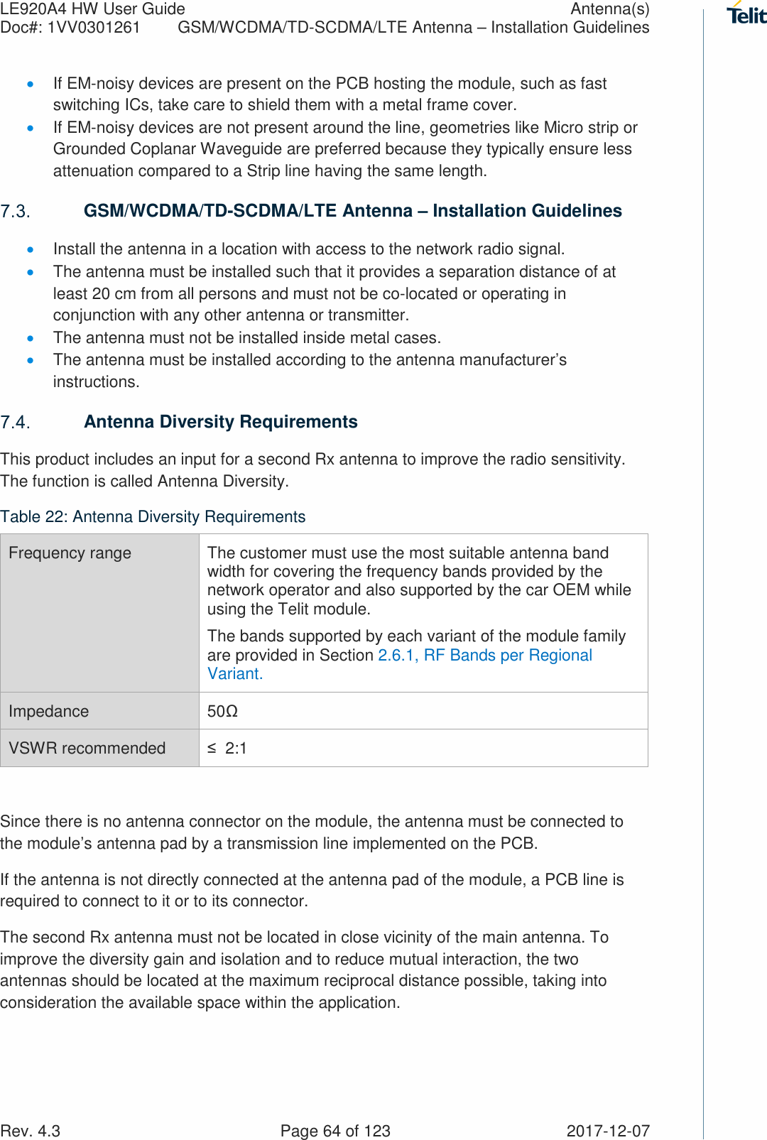
![LE920A4 HW User Guide Electrical Specifications Doc#: 1VV0301261 Logic Level Specifications Rev. 4.3 Page 44 of 123 2017-12-07 Pad Parameter Min Max Unit Comment RPU Pull-up resistance 10 100 [kΩ] RPD Pull-down resistance 10 100 [kΩ] Ci Input capacitance 5 [pF] 4.3.5. Dual Voltage Pads - Absolute Maximum Ratings Table 15: Absolute Maximum Ratings - Not Functional Parameter Min Max Input level on any digital pin when on -0.3V +3.6V Input voltage on analog pins when on -0.3V +3.6 V 4.3.6. SD Card Pads @ 2.95V Table 16: Operating Range – For SD Card Pads Operating at 2.95V Pad Parameter Min Max Unit Comments VIH Input high level 1.9V 3.1V [V] VIL Input low level -0.3V 0.7V [V] VOH Output high level 2.1V 3.05V [V] VOL Output low level 0V 0.4V [V] IIL Low-level input leakage current -10 [uA] No pull-up IIH High-level input leakage current 10 [uA] No pull-down RPU Pull-up resistance 10 100 [kΩ] RPD Pull-down resistance 10 100 [kΩ] Ci Input capacitance 5 [pF] 4.3.7. SIM Card Pads @2.95V Table 17: Operating Range – For SIM Pads Operating at 2.95V Pad Parameter Min Max Unit Comment VIH Input high level 2.1V 3.1V [V] VIL Input low level -0.3V 0.55V [V]](https://usermanual.wiki/Telit-Communications-S-p-A/LE920A4NA.User-manual/User-Guide-3744131-Page-44.png)
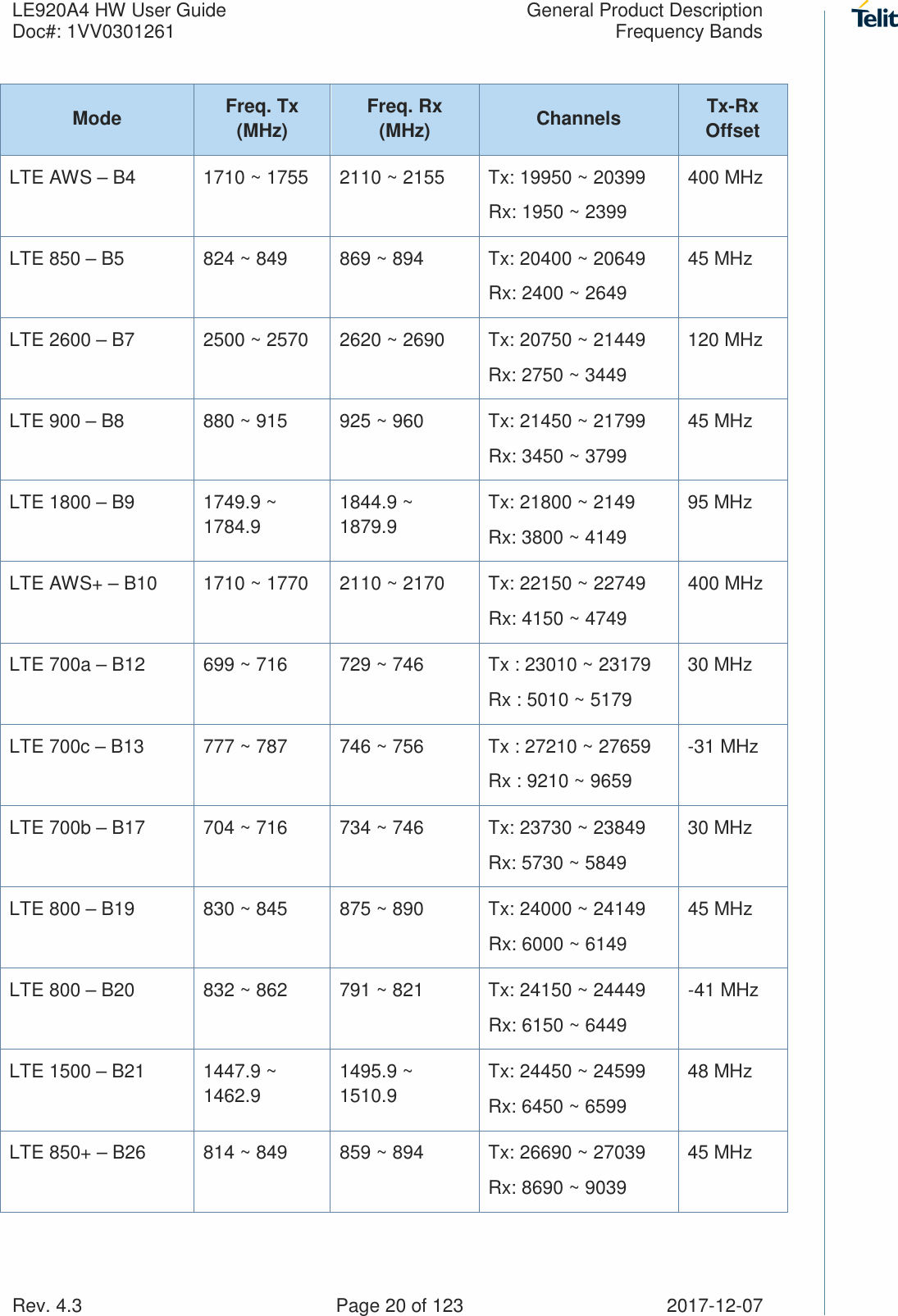
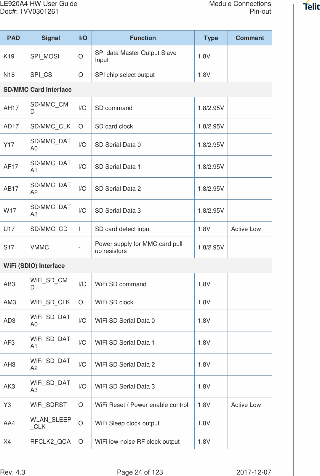
![LE920A4 HW User Guide Electrical Specifications Doc#: 1VV0301261 Logic Level Specifications Rev. 4.3 Page 45 of 123 2017-12-07 Pad Parameter Min Max Unit Comment VOH Output high level 2.25V 3.1V [V] VOL Output low level 0V 0.4V [V] IIL Low-level input leakage current -10 [uA] No pull-up IIH High-level input leakage current 10 [uA] No pull-down RPU Pull-up resistance 10 100 [kΩ] RPD Pull-down resistance 10 100 [kΩ] Ci Input capacitance 5 [pF]](https://usermanual.wiki/Telit-Communications-S-p-A/LE920A4NA.User-manual/User-Guide-3744131-Page-45.png)
![LE920A4 HW User Guide Conformity assessment issues Doc#: 1VV0301261 FCC/ISED Regulatory notices Rev. 4.3 Page 114 of 123 2017-12-07 14. Conformity assessment issues FCC/ISED Regulatory notices Modification statement Telit has not approved any changes or modifications to this device by the user. Any changes or modifications could void the user’s authority to operate the equipment. Telit n’approuve aucune modification apportée à l’appareil par l’utilisateur, quelle qu’en soit la nature. Tout changement ou modification peuvent annuler le droit d’utilisation de l’appareil par l’utilisateur. Interference statement (if it is not placed in the device) This device complies with Part 15 of the FCC Rules and Industry Canada licence-exempt RSS standard(s). Operation is subject to the following two conditions: (1) this device may not cause interference, and (2) this device must accept any interference, including interference that may cause undesired operation of the device. Le présent appareil est conforme aux CNR d'Industrie Canada applicables aux appareils radio exempts de licence. L'exploitation est autorisée aux deux conditions suivantes : (1) l'appareil ne doit pas produire de brouillage, et (2) l'utilisateur de l'appareil doit accepter tout brouillage radioélectrique subi, même si le brouillage est susceptible d'en compromettre le fonctionnement. Wireless notice This device complies with FCC/ISED radiation exposure limits set forth for an uncontrolled environment and meets the FCC radio frequency (RF) Exposure Guidelines and RSS-102 of the ISED radio frequency (RF) Exposure rules. Antenna gain must be below: Band Freq [MHz] Gain [dBi] GSM 850 850 3.64 EGPRS 850 850 3.64 PCS 1900 1900 2.51 EGPRS 1900 1900 2.51 WCDMA Band 2 1900 8.01 WCDMA Band 4 1700 5.00 WCDMA Band 5 850 5.00 FDD II 1900 8.01 FDD IV 1700 5.00 FDD V 850 5.00 FDD VII 700 8.01 FDD XII 700 5.63 This transmitter must not be co-located or operating in conjunction with any other antenna or transmitter. Le présent appareil est conforme à l'exposition aux radiations FCC / ISED définies pour un environnement non contrôlé et répond aux directives d'exposition de la fréquence de la FCC](https://usermanual.wiki/Telit-Communications-S-p-A/LE920A4NA.User-manual/User-Guide-3744131-Page-114.png)
![LE920A4 HW User Guide Conformity assessment issues Doc#: 1VV0301261 FCC/ISED Regulatory notices Rev. 4.3 Page 115 of 123 2017-12-07 radiofréquence (RF) et RSS-102 de la fréquence radio (RF) ISED règles d'exposition. Gain de l'antenne doit être ci-dessous: Band Freq [MHz] Gain [dBi] GSM 850 850 3.64 EGPRS 850 850 3.64 PCS 1900 1900 2.51 EGPRS 1900 1900 2.51 WCDMA Band 2 1900 8.01 WCDMA Band 4 1700 5.00 WCDMA Band 5 850 5.00 FDD II 1900 8.01 FDD IV 1700 5.00 FDD V 850 5.00 FDD VII 700 8.01 FDD XII 700 5.63 L'émetteur ne doit pas être colocalisé ni fonctionner conjointement avec à autre antenne ou autre émetteur. FCC Class B digital device notice This equipment has been tested and found to comply with the limits for a Class B digital device, pursuant to part 15 of the FCC Rules. These limits are designed to provide reasonable protection against harmful interference in a residential installation. This equipment generates, uses and can radiate radio frequency energy and, if not installed and used in accordance with the instructions, may cause harmful interference to radio communications. However, there is no guarantee that interference will not occur in a particular installation. If this equipment does cause harmful interference to radio or television reception, which can be determined by turning the equipment off and on, the user is encouraged to try to correct the interference by one or more of the following measures: - Reorient or relocate the receiving antenna. - Increase the separation between the equipment and receiver. - Connect the equipment into an outlet on a circuit different from that to which the receiver is connected. - Consult the dealer or an experienced radio/TV technician for help. LE920A4 NA Contains FCC ID: RI7LE920A4NA Contains IC: 5131A-LE920A4NA CAN ICES-3 (B) / NMB-3 (B) This Class B digital apparatus complies with Canadian ICES-003. Cet appareil numérique de classe B est conforme à la norme canadienne ICES -003.](https://usermanual.wiki/Telit-Communications-S-p-A/LE920A4NA.User-manual/User-Guide-3744131-Page-115.png)