Telit Communications S p A CC864-DUAL DUAL BAND CDMA/GPS module User Manual
Telit Communications S.p.A. DUAL BAND CDMA/GPS module
UserManual.wiki
>
Telit Communications S p A
>
CC864-DUAL User Manual
>
user manual
Contents
1.
User MAnual
2.
Users Manual
3.
User Manual
4.
user manual
user manual
Navigation menu
Upload a User Manual
Namespaces
Wiki Guide
HTML
PDF
Info
Views
User Manual
Discussion / Help
Navigation
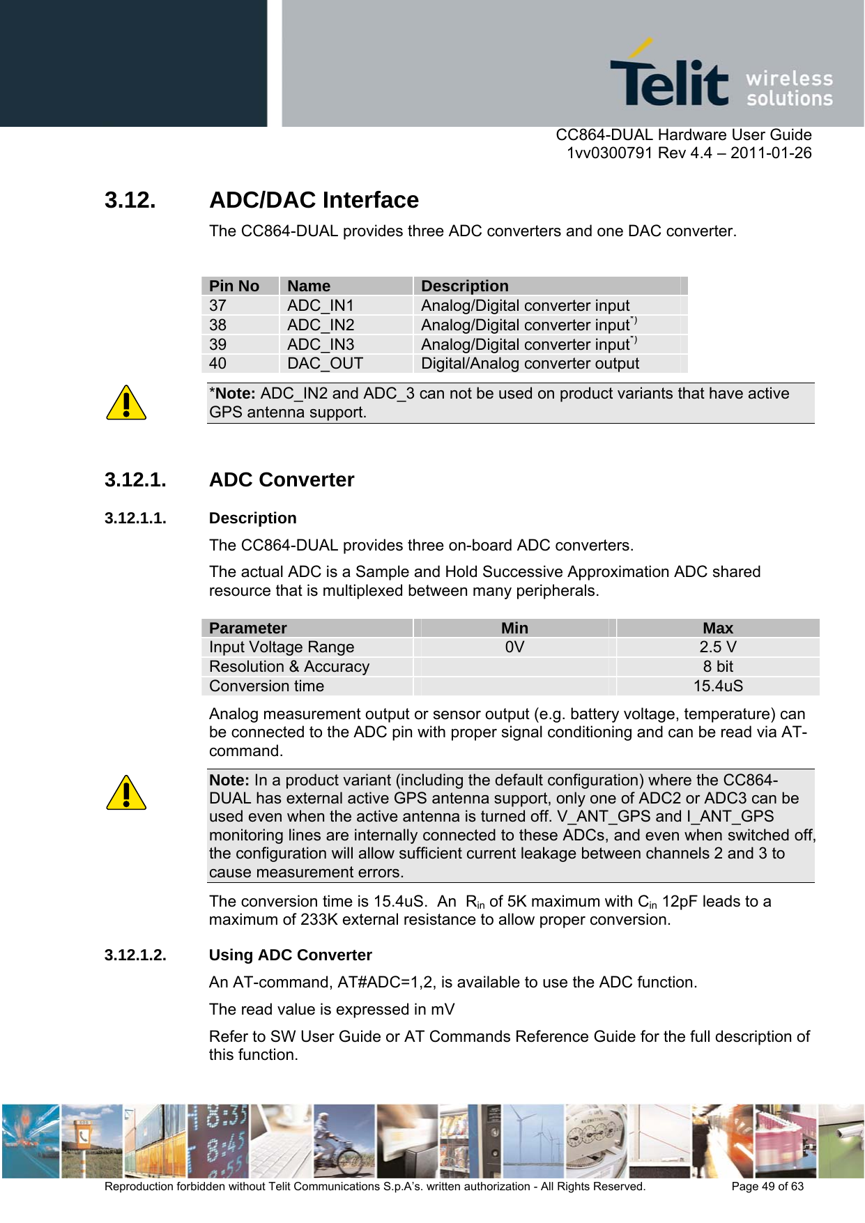
![CC864-DUAL Hardware User Guide 1vv0300791 Rev 4.4 – 2011-01-26 Reproduction forbidden without Telit Communications S.p.A’s. written authorization - All Rights Reserved. Page 50 of 63 3.12.2. DAC Converter 3.12.2.1. Description The CC864-DUAL provides a digital to analog converter (DAC). The DAC is a PDM output (Pulse Density Modulated DAC). Parameter Min Max Output Voltage Range 0V 2.6 V Resolution 8 bit PDM Clock rate 4.8Mhz The resolution is 8 bits so, as an example, if the maximum voltage is 2.6V, the integrated voltage could be calculated with the following formula: Integrated output voltage = (2.6 × value)/255 3.12.2.2. Enabling the DAC An AT-command is available to control the DAC function: AT#DAC[=<enable>[,<value>]] <value> - scale factor of the integrated output voltage(0…255 - 8 bit precision) and must be present if <enable>=1. Refer to the SW User Guide or AT Commands Reference Guide for the full description of this function. 3.12.2.3. Low Pass Filter Example The DAC pin drives the PDM (Pulse Density Modulation) signal. It is a square wave output. The application needs an additional RC filter to convert the PDM output to an analog signal. The figure below shows an example of a Low Pass filter. Final tuning is needed to find the exact values of resistors and capacitors for the target application.](https://usermanual.wiki/Telit-Communications-S-p-A/CC864-DUAL.user-manual/User-Guide-1428752-Page-50.png)