Telit Communications S p A CC864-DUAL DUAL BAND CDMA/GPS Module User Manual
Telit Communications S.p.A. DUAL BAND CDMA/GPS Module Users Manual
UserManual.wiki
>
Telit Communications S p A
>
CC864-DUAL User Manual
>
Users Manual
Contents
1.
User MAnual
2.
Users Manual
3.
User Manual
4.
user manual
Users Manual
Navigation menu
Upload a User Manual
Namespaces
Wiki Guide
HTML
PDF
Info
Views
User Manual
Discussion / Help
Navigation

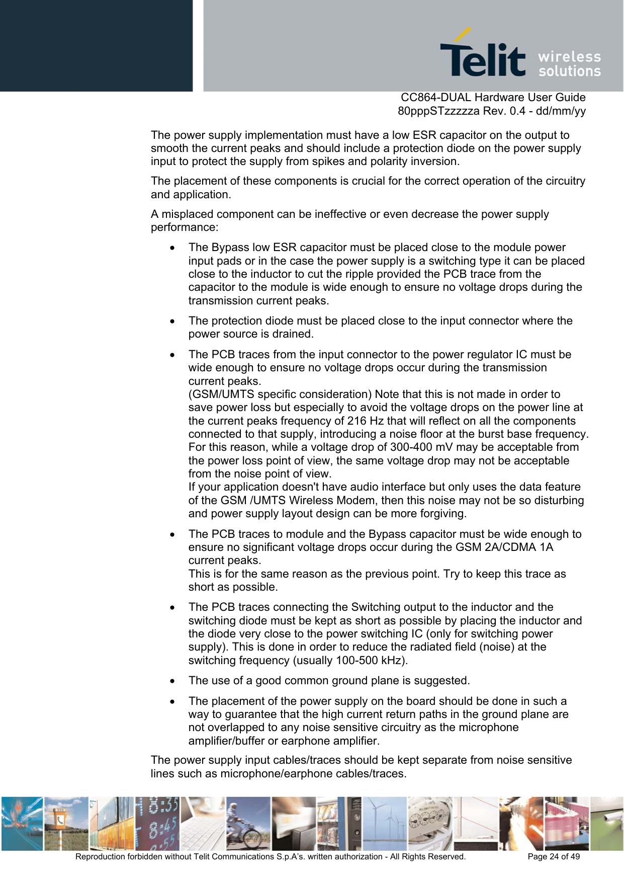
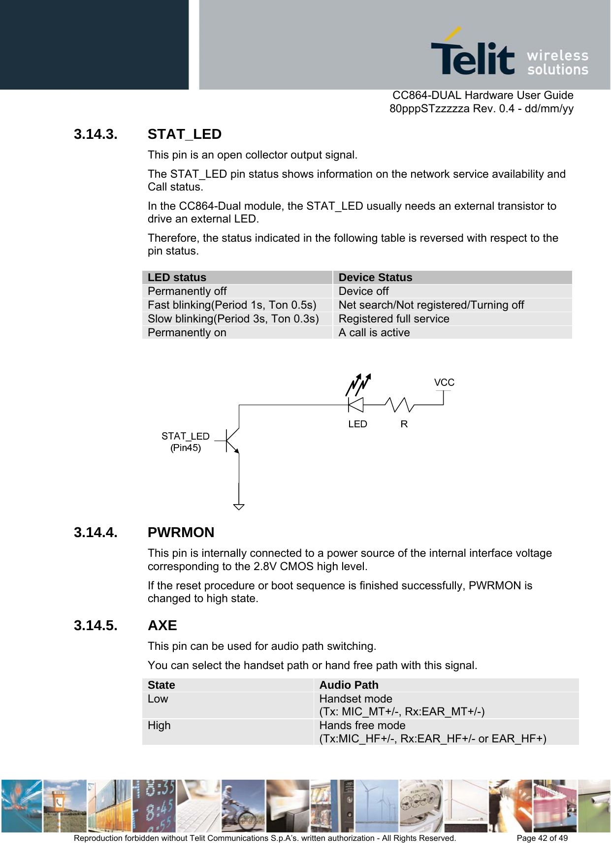
![CC864-DUAL Hardware User Guide 80pppSTzzzzza Rev. 0.4 - dd/mm/yy Reproduction forbidden without Telit Communications S.p.A’s. written authorization - All Rights Reserved. Page 35 of 49 AT-command is AT#DVI=<mode>[,<dviport>,<clockmode>]. Pin Number Name I/O Description Level 36 PCM_CLOCK I/O PCM_CLOCK CMOS 2.8V 63 TGPIO_10/PCM_TX I/O TGPIO10 Configurable GPIO/PCM_TX CMOS 2.8V 65 TGPIO_18/PCM_RX I/O TGPIO18 Configurable GPIO/PCM_RX CMOS 2.8V 71 TGPIO_17/PCM_SYNC I/O TGPIO17 Configurable GPIO/PCM_SYNC CMOS 2.8V 3.11. I2C Bus Interface The I2C is a two-wire bus for Inter-IC communication widely supported by peripheral components. Two wires (or lines); serial data (SDA) and serial clock (SCL) carry information between the connected devices. Each device is recognized by a unique address (whether it’s a microcontroller, memory, LCD driver, stereo DAC, or keyboard interface) and can operate as either a transmitter or receiver, depending on the device function. Pin No Name Description 33 SCL Serial BUS Clock 34 SDA Serial BUS Data 3.12. ADC/DAC Interface The CC864-Dual module provides three ADC converters and one DAC converter. Pin No Name Description 37 ADC_IN1 Analog/Digital converter input 38 ADC_IN2 Analog/Digital converter input 39 ADC_IN3 Analog/Digital converter input 40 DAC_OUT Digital/Analog converter output 3.12.1. ADC Converter 3.12.1.1. Description The CC864-Dual module provides three on-board ADC converters.](https://usermanual.wiki/Telit-Communications-S-p-A/CC864-DUAL.Users-Manual/User-Guide-970477-Page-36.png)
![CC864-DUAL Hardware User Guide 80pppSTzzzzza Rev. 0.4 - dd/mm/yy Reproduction forbidden without Telit Communications S.p.A’s. written authorization - All Rights Reserved. Page 36 of 49 Parameter Min Max Input Voltage Range 0V 2.5 V Resolution 10 bit Accuracy 8 bit Clock rate 2.4Mhz Analog measurement output or sensor output (battery voltage, temperature etc) can be connected to the ADC pin with proper signal conditioning and be read by an AT-command. 3.12.1.2. Using ADC Converter An AT-command is available to use the ADC function The command is AT#ADC=1,2 The read value is expressed in mV Refer to SW User Guide or AT Commands Reference Guide for the full description of this function. 3.12.2. DAC Converter 3.12.2.1. Description The CC864-Dual module provides a digital to analog converter (DAC). Parameter Min Max Input Voltage Range 0V 2.8 V Resolution 8 bit Clock rate 4.8Mhz The precision is 8 bits so, if we consider that the maximum voltage is 2V, the integrated voltage could be calculated with the following formula: Integrated output voltage = (2 × value)/255 3.12.2.2. Enabling the DAC An AT-command is available to use the DAC function The command is AT#DAC[=<enable>[,<value>]] <value> - scale factor of the integrated output voltage(0…255 -8 bit precision) and must be present if <enable>=1 Refer to the SW User Guide or AT commands Reference Guide for the full description of this function.](https://usermanual.wiki/Telit-Communications-S-p-A/CC864-DUAL.Users-Manual/User-Guide-970477-Page-37.png)