Spectralink PK4587 DECT 6.0 Module User Manual Produktionsflow for 1401 31XX CSLC SDX

Spectralink Corporation DECT 6.0 Module Produktionsflow for 1401 31XX CSLC SDX

Contents

15_KT4587-1 ClIIPCH_UserMan
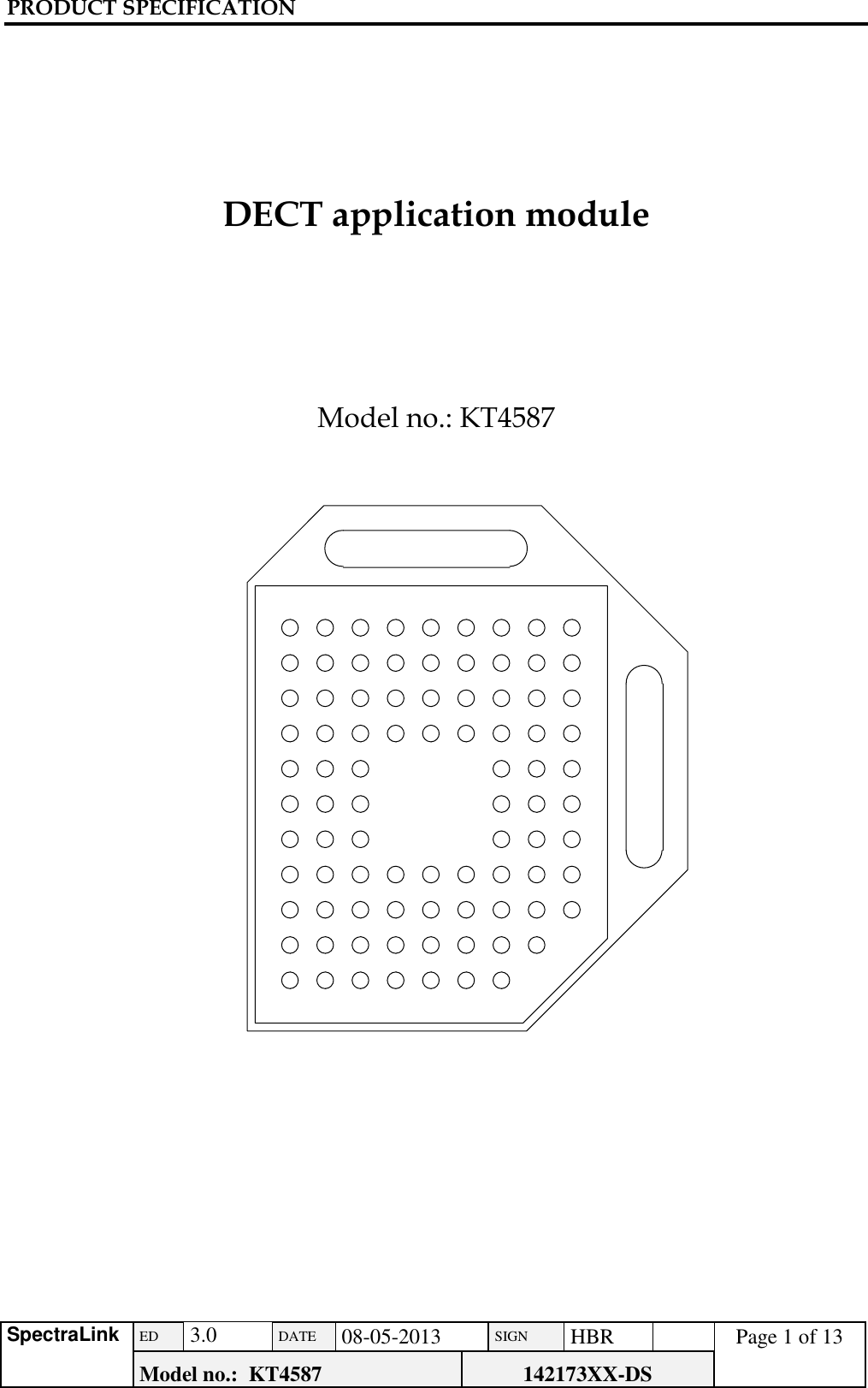
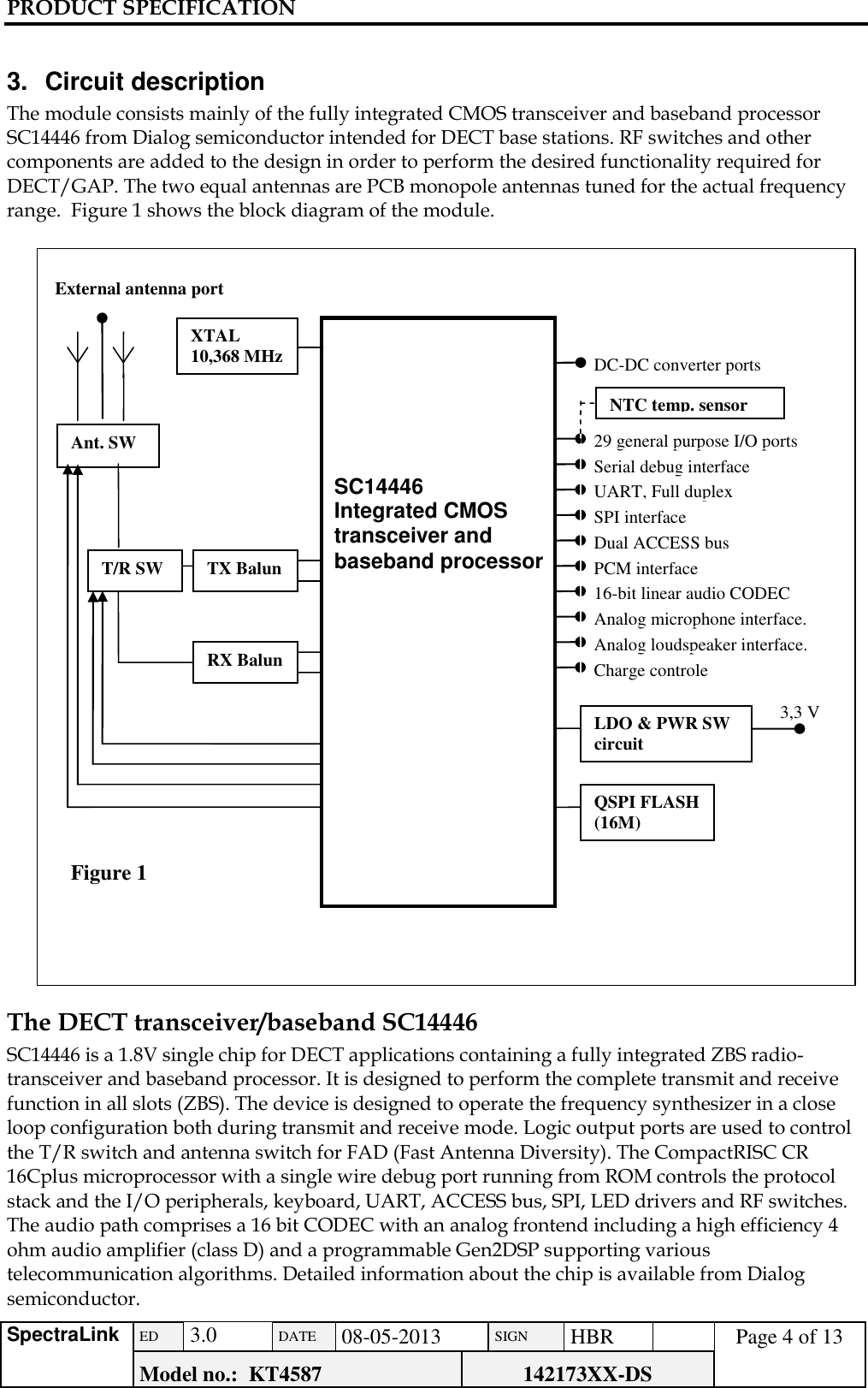
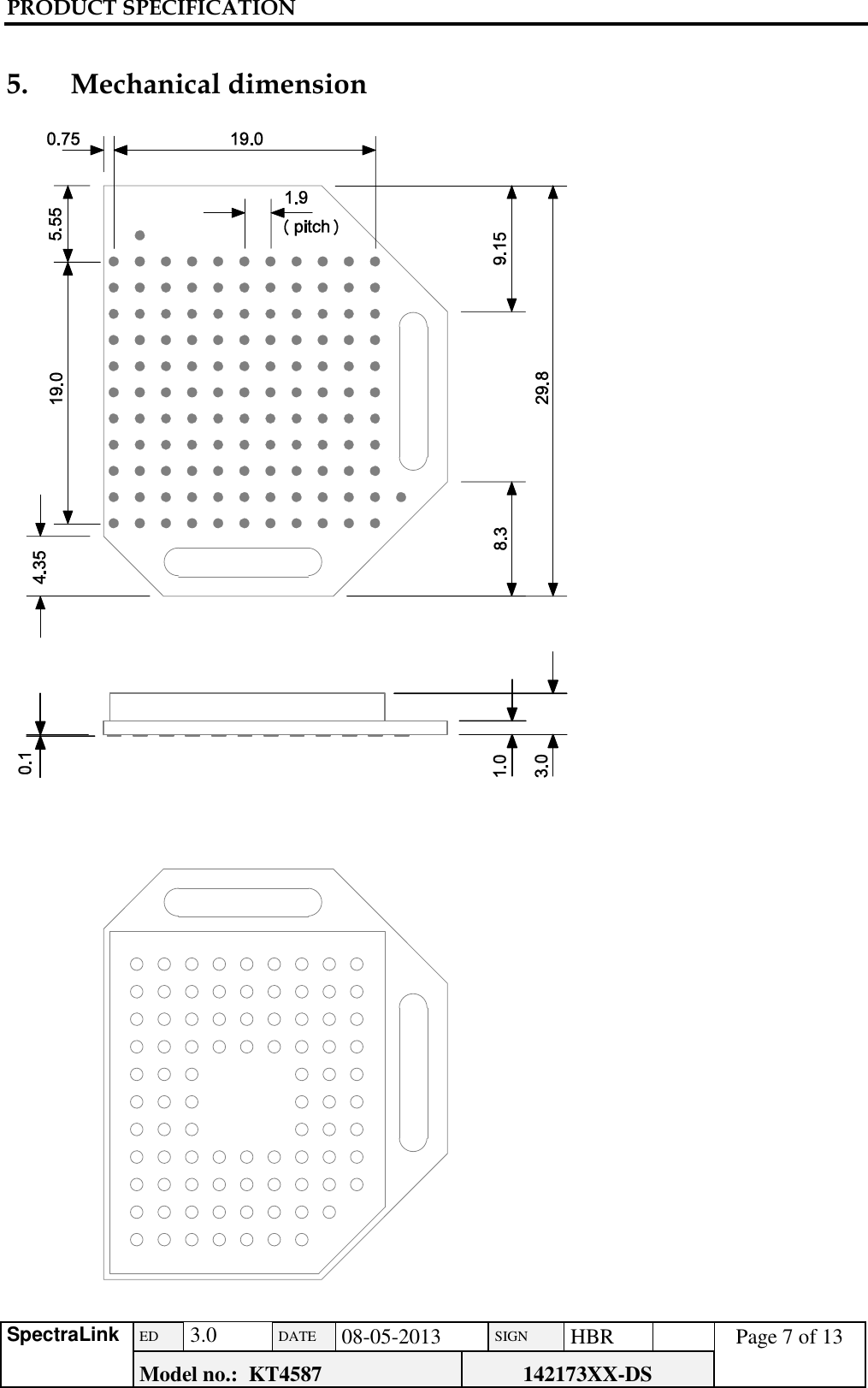
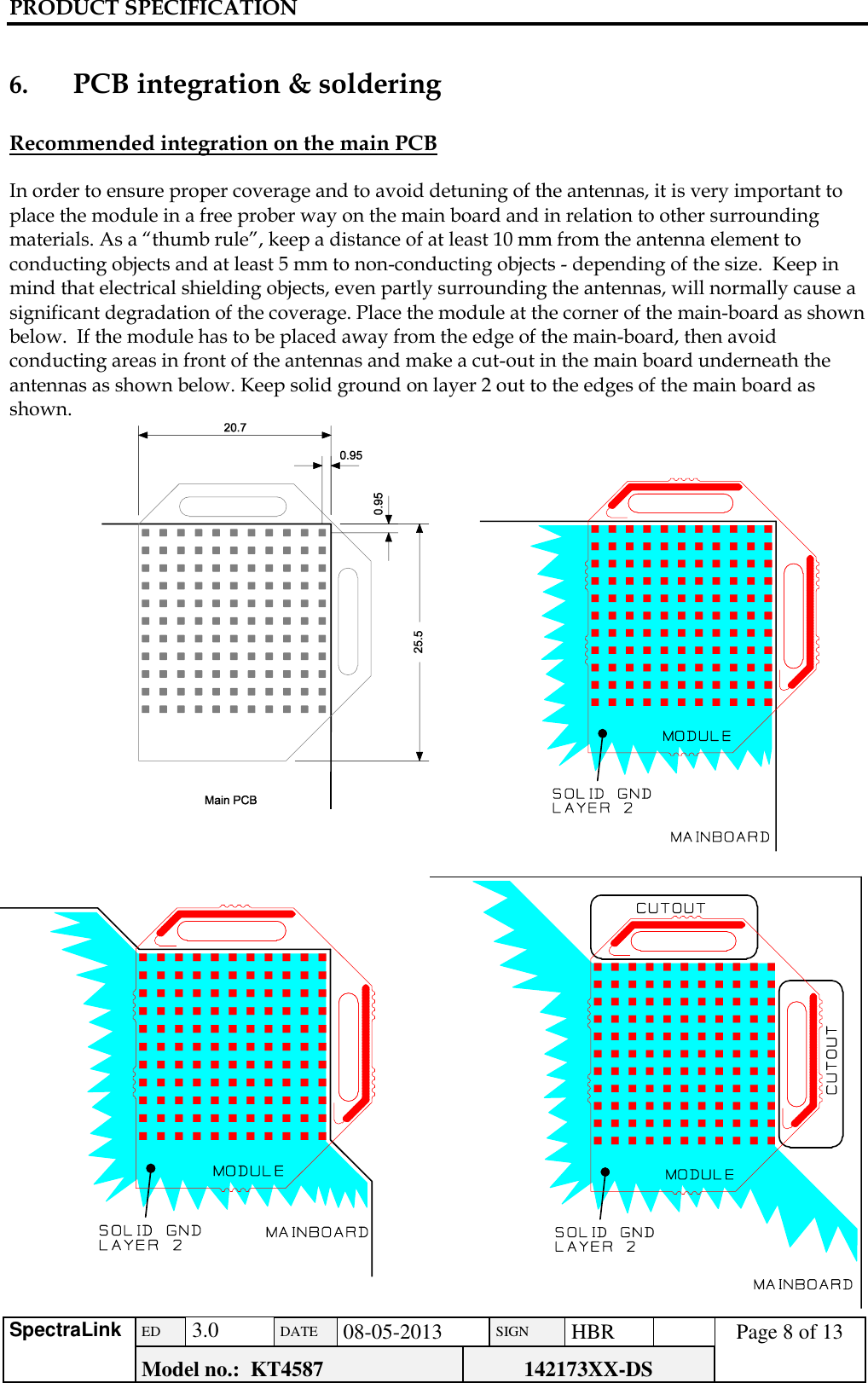
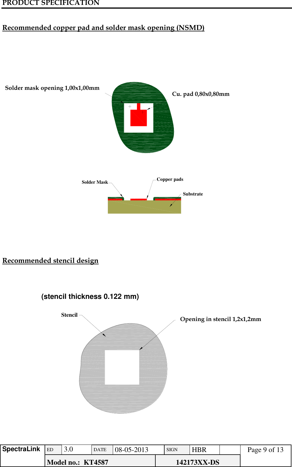
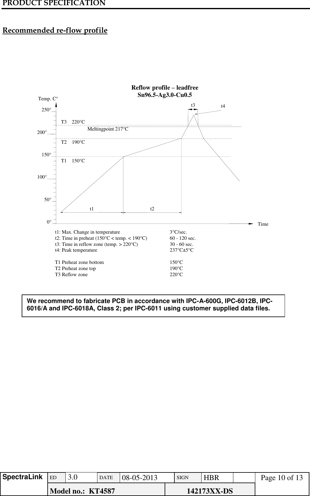
PRODUCT SPECIFICATION      SpectraLink ED  3.0 DATE 08-05-2013 SIGN HBR  Page 1 of 13 Model no.:  KT4587 142173XX-DS        DECT application module      Model no.: KT4587
PRODUCT SPECIFICATION      SpectraLink ED  3.0 DATE 08-05-2013 SIGN HBR  Page 2 of 13 Model no.:  KT4587 142173XX-DS     1. Preface ....................................................................................................................................... 3 2. Features ..................................................................................................................................... 3 3. Circuit description ..................................................................................................................... 4 4. Pin configuration .................................................................................................................... 5 5. Mechanical dimension............................................................................................................ 7 6. PCB integration & soldering ................................................................................................. 8 7. FCC compliance statement .................................................................................................. 11 8. Safety compliance statement .............................................................................................. 13                     Proprietary and Confidential  The information contained herein is the sole intellectual property of SpectraLink. No distribution, reproduction or unauthorized use of these materials is permitted without the expressed written consent of SpectraLink. Information contained herein is subject to change without notice and does not represent commitment of any type on the part of SpectraLink.  SpectraLink and Accord are registered trademarks of SpectraLink.   Notice  While reasonable effort was made to ensure that the information in this document was complete and accurate at the time of printing, SpectraLink, cannot assume responsibility for any errors. Changes and/or corrections to the information contained in this document may be incorporated into future issues.
PRODUCT SPECIFICATION      SpectraLink ED  3.0 DATE 08-05-2013 SIGN HBR  Page 3 of 13 Model no.:  KT4587 142173XX-DS     1.  Preface  The KT4587, DECT application module is used to transfer messaging, data, and voice signals by use of the radio frequency spectrum according to the DECT standard.  KT4587 is a fully approved module that complies with the following standards and certifications: EN 301 406 V2.1.1:2009-07 (DECT radio)  EN 300 175-1 to 8 (DECT CI)  EN 301 489-1 V1.8.1:2008-04, EN 301 489-6 V1.3.1:2008-08 (EMC) IEC 60950-1:2005 (ed. 2.0) +am1:2009, EN 60950-1:2006+A11:2009+A1:2010 (Safety) R&TTE certificate  FCC PART 15, Subpart D FCC part 15B FCC SAR RSS-213  This means that by integration on a main board no radio test is required.      2.  Features  RF range:      1880 – 1930 MHz DECT channels:    120(EU) 60(US) logical duplex channels. Receiver sensitivity:    Typ.< -93 dBm [BER,1000 ppm].  Transmit power (NTP):    Typ. 23 dBm. , 20.2 dBm (US) Power supply range:    3.2 – 3.45V Current consumption:    TBD    Temp. Range:    -20ºC to +85ºC. Size:      25.0 X 30.0 X 3.0mm. Other features:   See data sheet for SC14446      External antenna option
PRODUCT SPECIFICATION      SpectraLink ED  3.0 DATE 08-05-2013 SIGN HBR  Page 4 of 13 Model no.:  KT4587 142173XX-DS    3.  Circuit description The module consists mainly of the fully integrated CMOS transceiver and baseband processor SC14446 from Dialog semiconductor intended for DECT base stations. RF switches and other components are added to the design in order to perform the desired functionality required for DECT/GAP. The two equal antennas are PCB monopole antennas tuned for the actual frequency range.  Figure 1 shows the block diagram of the module.   The DECT transceiver/baseband SC14446 SC14446 is a 1.8V single chip for DECT applications containing a fully integrated ZBS radio-transceiver and baseband processor. It is designed to perform the complete transmit and receive function in all slots (ZBS). The device is designed to operate the frequency synthesizer in a close loop configuration both during transmit and receive mode. Logic output ports are used to control the T/R switch and antenna switch for FAD (Fast Antenna Diversity). The CompactRISC CR 16Cplus microprocessor with a single wire debug port running from ROM controls the protocol stack and the I/O peripherals, keyboard, UART, ACCESS bus, SPI, LED drivers and RF switches. The audio path comprises a 16 bit CODEC with an analog frontend including a high efficiency 4 ohm audio amplifier (class D) and a programmable Gen2DSP supporting various telecommunication algorithms. Detailed information about the chip is available from Dialog semiconductor.   T/R SW 29 general purpose I/O ports Figure 1   SC14446 Integrated CMOS transceiver and baseband processor Ant. SW Serial debug interface UART, Full duplex SPI interface Dual ACCESS bus PCM interface 16-bit linear audio CODEC Analog microphone interface. Analog loudspeaker interface. Charge controle LDO & PWR SW circuit 3,3 V QSPI FLASH (16M) RX Balun TX Balun DC-DC converter ports XTAL 10,368 MHz External antenna port NTC temp. sensor
PRODUCT SPECIFICATION      SpectraLink ED  3.0 DATE 08-05-2013 SIGN HBR  Page 5 of 13 Model no.:  KT4587 142173XX-DS    4.     Pin configuration    A1 GND B1 GND C1 GND D1 GND E1 VDDPA F1 SOCp A2 GND B2 GND C2 P30 D2 P31 E2 GND F2 P10 A3 GND B3 CP_VOUT1 C3 GND D3 P16 E3 CHARGE_CTRL F3 ADC2 A4 CP_VOUT2 B4 P15 C4 P27 D4 P17 E4 SOCn F4 DC_CTRLN A5 VDDIO B5 GND C5 P14 D5 GND E5 GND F5 ULP_PORT A6 P12 B6 P26 C6 P11 D6 GND E6 GND F6 ULP_VBAT A7 GND B7 P05 C7 GND D7 GND E7 GND F7 ULP_MAIN_CTRL A8 GND B8 GND C8 P00 D8 GND E8 GND F8 RFP0n A9 VBAT B9 P01 C9 GND D9 P24 E9 GND F9 P23 A10 P04 B10 VBATT C10 JTAG D10 VDD E10 P07 F10 P13 A11 RSTn B11 GND C11 VCCRF D11 P25 E11 GND F11 P06   B12 TP2         G1 GND H1 VREFm J1 GND K1 VREFp L1 GND   G2 LSRn H2 LSRp J2 MICh K2 MICp L2 MICn M2 TP1 G3 GND H3 P37 J3 GND K3 P32_CIDINp L3 GND   G4 P33 H4 ONE_CELL J4 P35 K4 P36 L4 GND   G5 GND H5 DC_SENCE J5 GND K5 P34 L5 RFP0   G6 DC_CTRL H6 DC_I J6 RFP1 K6 WLED0 L6 GND   G7 GND H7 P22 J7 GND K7 WLED1 L7 GND   G8 LDORF_CTRL H8 RFP2 J8 P21 K8 P20 L8 WLED2   G9 GND H9 GND J9 GND K9 GND L9 GND   G10 GND H10 GND J10 GND K10 RF0 L10 RF1   G11 GND H11 GND J11 GND K11 RF2 L11 GND                              Leave K10, K11, L10, M2 and B12 (RF ports and test pin’s) unconnected to the main board without any conducting plan underneath.  Connect VREFm to local GND on the main board.
PRODUCT SPECIFICATION      SpectraLink ED  3.0 DATE 08-05-2013 SIGN HBR  Page 6 of 13 Model no.:  KT4587 142173XX-DS    Top view of the pin’s
PRODUCT SPECIFICATION      SpectraLink ED  3.0 DATE 08-05-2013 SIGN HBR  Page 7 of 13 Model no.:  KT4587 142173XX-DS    5.     Mechanical dimension
PRODUCT SPECIFICATION      SpectraLink ED  3.0 DATE 08-05-2013 SIGN HBR  Page 8 of 13 Model no.:  KT4587 142173XX-DS    6.     PCB integration & soldering      Recommended integration on the main PCB  In order to ensure proper coverage and to avoid detuning of the antennas, it is very important to place the module in a free prober way on the main board and in relation to other surrounding materials. As a “thumb rule”, keep a distance of at least 10 mm from the antenna element to conducting objects and at least 5 mm to non-conducting objects - depending of the size.  Keep in mind that electrical shielding objects, even partly surrounding the antennas, will normally cause a significant degradation of the coverage. Place the module at the corner of the main-board as shown below.  If the module has to be placed away from the edge of the main-board, then avoid conducting areas in front of the antennas and make a cut-out in the main board underneath the antennas as shown below. Keep solid ground on layer 2 out to the edges of the main board as shown.
PRODUCT SPECIFICATION      SpectraLink ED  3.0 DATE 08-05-2013 SIGN HBR  Page 9 of 13 Model no.:  KT4587 142173XX-DS   Cu. pad 1.00x1.00mmSolder mask opening 1.80x1.80mmSubstrateCopper padsSolder MaskStencil Opening in stencil 1.40 x 1,40mm Recommended copper pad and solder mask opening (NSMD)                           Recommended stencil design         (stencil thickness 0.122 mm)                        Cu. pad 0,80x0,80mm       Solder mask opening 1,00x1,00mm Opening in stencil 1,2x1,2mm
PRODUCT SPECIFICATION      SpectraLink ED  3.0 DATE 08-05-2013 SIGN HBR  Page 10 of 13 Model no.:  KT4587 142173XX-DS     Recommended re-flow profile                                                         t1: Max. Change in temperature 3°C/sec. t2: Time in preheat (150°C < temp. < 190°C) 60 - 120 sec. t3: Time in reflow zone (temp. > 220°C) 30 - 60 sec. t4: Peak temperature 237°C±5°C T1 Preheat zone bottom 150°C T2 Preheat zone top 190°C T3 Reflow zone 220°C 0° T1    150°C T2    190°C T3    220°C 50° t1 t2 Meltingpoint 217°C 150° 100° 250° 200° Reflow profile – leadfree Sn96.5-Ag3.0-Cu0.5 t3 t4 Temp. C° Time We recommend to fabricate PCB in accordance with IPC-A-600G, IPC-6012B, IPC-6016/A and IPC-6018A, Class 2; per IPC-6011 using customer supplied data files.
PRODUCT SPECIFICATION      SpectraLink ED  3.0 DATE 08-05-2013 SIGN HBR  Page 11 of 13 Model no.:  KT4587 142173XX-DS    7.     FCC compliance statement  This device complies with Part 15 of the FCC Rules Operation is subject to the following two conditions:  (1) this device may not cause interference, and (2) this device must accept any interference, including interference that may cause undesired operation of the device.  Information to User: This equipment has been tested and found to comply with the limits for a Class B digital device, pursuant to Part 15 of the FCC Rules. These limits are designed to provide reasonable protection against harmful interference in a residential installation. This equipment generates, uses and can radiate radio frequency energy and, if not installed and used in accordance with the instructions, may cause harmful interference to radio communications. However, there is no guarantee that interference will not occur in a particular installation. If this equipment does cause harmful interference to radio or television reception, which can be determined by turning the equipment off and on, the user is encouraged to try to correct the interference by one or more of the following measures: - Reorient or relocate the receiving antenna - Increase the separation between the equipment and receiver - Connect the equipment into an outlet on a circuit different from that to which the receiver is connected. - Consult the dealer or an experienced radio/TV technician for help.  FCC / IC Canada Labeling of host device: The modular transmitter is labeled with its own FCC and IC identification number, and, if the FCC or IC identification numbers are not visible when the module is installed inside another device, then the outside of the device into which the module is installed must also display a label referring to the enclosed module. This exterior label shall use wording as the following: “Contains FCC ID: PXA-PK4587 and Contains IC: 4604A-PK4587”.    RF Exposure information: The internal antennas used for this mobile transmitter must provide a separation distance of at least 20 cm from all persons. OEM integrators and end users must be provided with transmitter operating conditions for satisfying RF exposure compliance.  Antenna information: The module has been tested and approved for use with the antenna listed below:  Type of antennas:  PCB monopole antenna. Gain of the antennas:  1.2 dBi  Frequency range:  1920-1930 MHz  The use of that module in combination with a not listed antenna must be authorized with respective regulatory agencies.
PRODUCT SPECIFICATION      SpectraLink ED  3.0 DATE 08-05-2013 SIGN HBR  Page 12 of 13 Model no.:  KT4587 142173XX-DS   Déclaration de conformité FCC Cet appareil est conforme à la section 15 des règlements FCC Le fonctionnement est soumis aux deux conditions suivantes : (1) cet appareil ne doit pas causer d'interférences, et (2) cet appareil doit accepter toute autre interférence, y compris les interférences pouvant entraîner un fonctionnement non désiré de l'appareil.  Informations pour l'utilisateur : Cet équipement a été testé et respecte les limitations d'un appareil numérique de classe B, conformément à la section  des règlements FCC. Ces limitations sont destinées à assurer une protection raisonnable contre les interférences nuisibles dans une installation résidentielle. Cet équipement produit, utilise et peut émettre de l'énergie de fréquence radio et, s'il n'est pas installé et utilisé conformément aux instructions, peut causer des interférences nuisibles aux communications radio. Cependant, il est impossible de garantir que des interférences ne se produiront pas dans certaines installations. Si cet équipement cause des interférences nuisibles à la réception radio ou de télévision, ce qui peut être déterminé en allumant et éteignant l'appareil, l'utilisateur est encouragé d'essayer de corriger les interférences à l'aide d'une ou plusieurs des mesures suivantes : - Réorientez ou repositionnez l'antenne de réception - Augmentez l'espacement entre l'équipement et le récepteur - Connectez l'équipement sur la prise d'un circuit différent que celui du récepteur - Consulter le revendeur ou un technicien radio / télévision qualifié pour obtenir de l'aide.  Marquage FCC / IC Canada sur appareil d'accueil : Le transmetteur modulaire est marqué avec son propre numéro d'identification FCC et IC et, si les numéros d'identification FCC et IC ne sont pas visibles lorsque le module est installé dans un autre appareil, l'extérieur de l'appareil dans lequel le module est installé doit aussi porter un étiquette faisant référence au module. Cette étiquette extérieure doit utiliser le libellé suivant : “Contient FCC ID: PXA-PK4587 et contient IC: 4604A-PK4587”.   Informations sur l'exposition RF : Les antennes internes utilisées pour ce transmetteur mobile doivent offrir une distance de séparation d'au moins 20 cm de toute personne. Les conditions de fonctionnement d'émetteur offertes aux intégrateurs OEM et aux utilisateurs finaux doivent satisfaire les normes d'exposition RF.  Information d'antenne : Le module a été testé et approuvé pour une utilisation avec l'antenne ci-dessous: Type d'antennes : Antenne monopôle PCB. Gain des antennes: 1,2 dBi Portée de fréquence : 1920-1930 MHz L'utilisation de ce module en combinaison avec une antenne non listée doit être autorisée par les organismes de réglementation correspondants.
PRODUCT SPECIFICATION      SpectraLink ED  3.0 DATE 08-05-2013 SIGN HBR  Page 13 of 13 Model no.:  KT4587 142173XX-DS    8.     Safety compliance statement   1) The specific external power supply for the DECT application module KT4585A has to fulfil the requirements according to clause 2.5 (Limited power source) of this standard EN 60950-1:2006.  2) Interconnection circuits shall be selected to provide continued conformance to the requirements of clause 2.2 for SELV (Safety Extra Low Voltage) circuits according to EN 60950-1:2006 after making connections.   3) Interface type not subjected to over voltages (i.e. does not leave the building).  4) Requirements additional to those specified in this standard may be necessary for:  -  Equipment intended for operation in special environments (for example, extremes of temperature, excessive dust, moisture or vibration, flammable gases and corrosive or explosive atmospheres). -  Equipment intended to be used in vehicles, on board ships or aircraft, in tropical countries or at altitudes grater than 2000 m. -  Equipment intended for use where ingress of water is possible.  5) Installation by qualified personnel only!  6) The product is a component intended for installation and use in complete equipment. The final acceptance of the component is dependent upon its installation and use in complete equipment.

Navigation menu