Simcom 201606 LTE-FDD/HSPA MODULE User Manual SIM7500A V1 00 20160930

Shanghai Simcom Ltd. LTE-FDD/HSPA MODULE SIM7500A V1 00 20160930

Contents

SIM7500A__User Manual_V1 00_20160930
SIM7500A_User Manual_V1.02
Smart Machine Smart DecisionSIM7500A_User Manual_V1.022016-09-292Document TitleSIM7500A_User ManualVersionV1.02Date2016-09-29StatusReleasedDocument Control IDSIM7500A_User Manual_V1.02General NotesSIMCom offers this information as a service to its customers to support the application andengineering efforts that use the products designed by SIMCom. The information provided is basedon the requirements specifically from the customers. SIMCom has not undertaken any independentsearch for additional relevant information, including any information that may be in the customer’spossession. Furthermore, the system validation of the product designed by SIMCom within a largerelectronic system remains the responsibility of the customer or the customer’s system integrator.All specifications supplied herein are subject to change without notice.CopyrightThis document contains the proprietary technical information which is the property of SIMComLimited, copying of this document, giving it to others, the using or communication of the contentsthereof are forbidden without the official authority by SIMCom. Offenders are liable to thepayment of the damages. All rights are reserved in the event of grant of a patent or the registrationof a utility model or design. All specifications supplied herein are subject to change without noticeCopyright © SIMCom Wireless Solutions Co., Ltd. 2016
Smart Machine Smart DecisionSIM7500A_User Manual_V1.022016-09-293ContentsContents............................................................................................................................................... 3Table Index.......................................................................................................................................... 5Figure Index........................................................................................................................................ 6Revision History..................................................................................................................................71 Introduction..................................................................................................................................81.1 Product Outline....................................................................................................................... 81.2 Hardware Interface Overview.................................................................................................81.3 Hardware Block Diagram....................................................................................................... 81.4 Functional Overview...............................................................................................................92 Package Information................................................................................................................. 112.1 Pin Assignment Overview.....................................................................................................112.2 Pin Description......................................................................................................................132.3 Mechanical Information........................................................................................................152.4 Footprint Recommendation.................................................................................................. 163 Interface Application.................................................................................................................173.1 Power Supply........................................................................................................................ 173.1.1 Power supply Design Guide.......................................................................................... 173.1.2 Recommended Power Supply Circuit............................................................................183.1.3 Voltage Monitor............................................................................................................. 193.2 Power on/Power off/Reset Function.....................................................................................193.2.1 Power on........................................................................................................................ 193.2.2 Power off........................................................................................................................203.2.3 Reset Function................................................................................................................213.3 UART Interface.....................................................................................................................223.3.1 UART Design Guide......................................................................................................223.3.2 RI and DTR Behavior.................................................................................................... 243.4 USB Interface........................................................................................................................243.4.1 USB Application Guide................................................................................................. 253.5 USIM Interface..................................................................................................................... 253.5.1 USIM Application Guide............................................................................................... 263.5.2 SIM Card Design Guide................................................................................................ 263.5.3 Recommended USIM Card Holder............................................................................... 273.6 PCM Interface.......................................................................................................................283.6.1 PCM Timing...................................................................................................................283.6.2 PCM Application Guide.................................................................................................293.7 I2C Interface......................................................................................................................... 303.7.1 I2C Design Guide.......................................................................................................... 303.8 Network Status......................................................................................................................313.9 Operating Status Indication.................................................................................................. 313.10 Pin Multiplex Function......................................................................................................313.11 Other interface................................................................................................................... 32
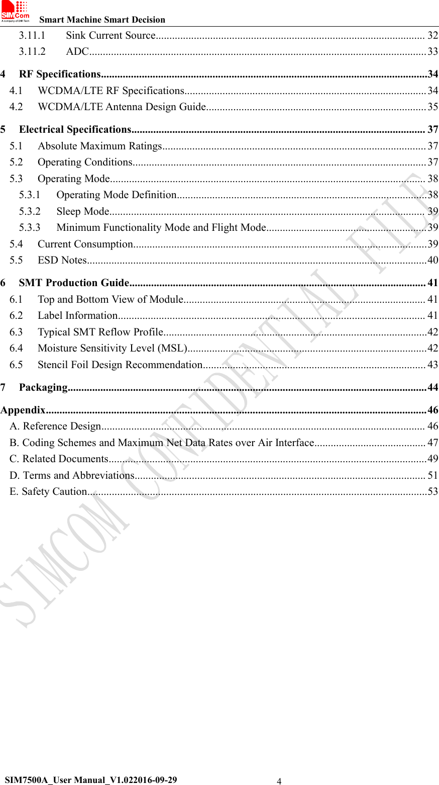
Smart Machine Smart DecisionSIM7500A_User Manual_V1.022016-09-2943.11.1 Sink Current Source................................................................................................... 323.11.2 ADC............................................................................................................................334 RF Specifications........................................................................................................................344.1 WCDMA/LTE RF Specifications.........................................................................................344.2 WCDMA/LTE Antenna Design Guide.................................................................................355 Electrical Specifications............................................................................................................ 375.1 Absolute Maximum Ratings................................................................................................. 375.2 Operating Conditions............................................................................................................375.3 Operating Mode.................................................................................................................... 385.3.1 Operating Mode Definition............................................................................................385.3.2 Sleep Mode.................................................................................................................... 395.3.3 Minimum Functionality Mode and Flight Mode...........................................................395.4 Current Consumption............................................................................................................395.5 ESD Notes.............................................................................................................................406 SMT Production Guide............................................................................................................. 416.1 Top and Bottom View of Module......................................................................................... 416.2 Label Information................................................................................................................. 416.3 Typical SMT Reflow Profile.................................................................................................426.4 Moisture Sensitivity Level (MSL)........................................................................................426.5 Stencil Foil Design Recommendation.................................................................................. 437 Packaging....................................................................................................................................44Appendix............................................................................................................................................46A. Reference Design....................................................................................................................... 46B. Coding Schemes and Maximum Net Data Rates over Air Interface......................................... 47C. Related Documents.....................................................................................................................49D. Terms and Abbreviations........................................................................................................... 51E. Safety Caution.............................................................................................................................53
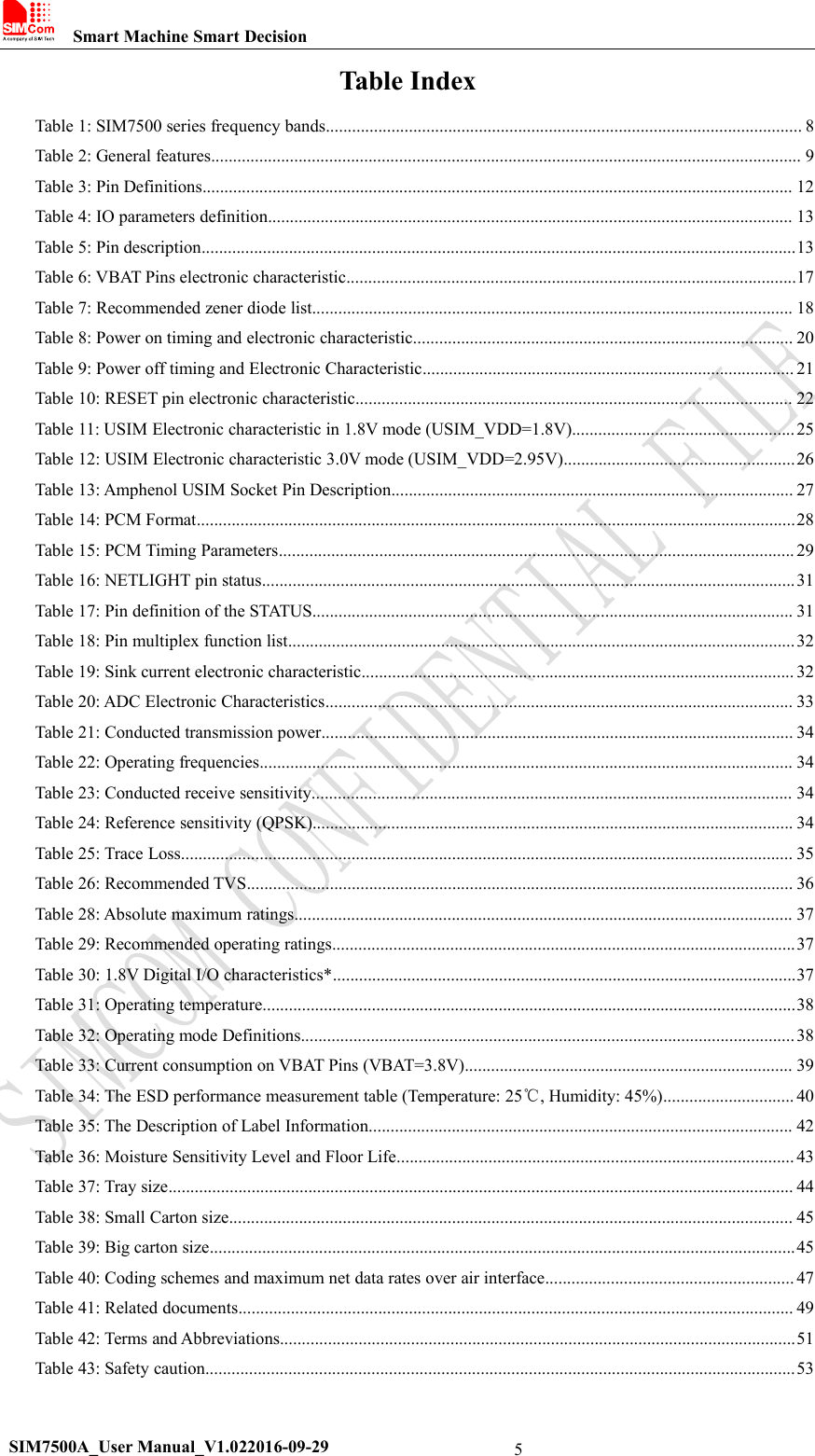
Smart Machine Smart DecisionSIM7500A_User Manual_V1.022016-09-295Table IndexTable 1: SIM7500 series frequency bands............................................................................................................. 8Table 2: General features....................................................................................................................................... 9Table 3: Pin Definitions....................................................................................................................................... 12Table 4: IO parameters definition........................................................................................................................ 13Table 5: Pin description........................................................................................................................................13Table 6: VBAT Pins electronic characteristic.......................................................................................................17Table 7: Recommended zener diode list.............................................................................................................. 18Table 8: Power on timing and electronic characteristic....................................................................................... 20Table 9: Power off timing and Electronic Characteristic..................................................................................... 21Table 10: RESET pin electronic characteristic.................................................................................................... 22Table 11: USIM Electronic characteristic in 1.8V mode (USIM_VDD=1.8V)...................................................25Table 12: USIM Electronic characteristic 3.0V mode (USIM_VDD=2.95V).....................................................26Table 13: Amphenol USIM Socket Pin Description............................................................................................ 27Table 14: PCM Format.........................................................................................................................................28Table 15: PCM Timing Parameters...................................................................................................................... 29Table 16: NETLIGHT pin status..........................................................................................................................31Table 17: Pin definition of the STATUS.............................................................................................................. 31Table 18: Pin multiplex function list....................................................................................................................32Table 19: Sink current electronic characteristic................................................................................................... 32Table 20: ADC Electronic Characteristics........................................................................................................... 33Table 21: Conducted transmission power............................................................................................................ 34Table 22: Operating frequencies.......................................................................................................................... 34Table 23: Conducted receive sensitivity.............................................................................................................. 34Table 24: Reference sensitivity (QPSK).............................................................................................................. 34Table 25: Trace Loss............................................................................................................................................ 35Table 26: Recommended TVS............................................................................................................................. 36Table 28: Absolute maximum ratings.................................................................................................................. 37Table 29: Recommended operating ratings..........................................................................................................37Table 30: 1.8V Digital I/O characteristics*..........................................................................................................37Table 31: Operating temperature..........................................................................................................................38Table 32: Operating mode Definitions................................................................................................................. 38Table 33: Current consumption on VBAT Pins (VBAT=3.8V)........................................................................... 39Table 34: The ESD performance measurement table (Temperature: 25℃, Humidity: 45%).............................. 40Table 35: The Description of Label Information................................................................................................. 42Table 36: Moisture Sensitivity Level and Floor Life........................................................................................... 43Table 37: Tray size............................................................................................................................................... 44Table 38: Small Carton size................................................................................................................................. 45Table 39: Big carton size......................................................................................................................................45Table 40: Coding schemes and maximum net data rates over air interface......................................................... 47Table 41: Related documents............................................................................................................................... 49Table 42: Terms and Abbreviations......................................................................................................................51Table 43: Safety caution.......................................................................................................................................53
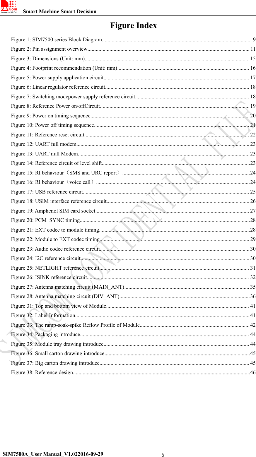
Smart Machine Smart DecisionSIM7500A_User Manual_V1.022016-09-296Figure IndexFigure 1: SIM7500 series Block Diagram............................................................................................................. 9Figure 2: Pin assignment overview...................................................................................................................... 11Figure 3: Dimensions (Unit: mm)........................................................................................................................ 15Figure 4: Footprint recommendation (Unit: mm)................................................................................................ 16Figure 5: Power supply application circuit.......................................................................................................... 17Figure 6: Linear regulator reference circuit......................................................................................................... 18Figure 7: Switching modepower supply reference circuit................................................................................... 18Figure 8: Reference Power on/offCircuit.............................................................................................................19Figure 9: Power on timing sequence....................................................................................................................20Figure 10: Power off timing sequence................................................................................................................. 21Figure 11: Reference reset circuit........................................................................................................................ 22Figure 12: UART full modem.............................................................................................................................. 23Figure 13: UART null Modem............................................................................................................................. 23Figure 14: Reference circuit of level shift............................................................................................................23Figure 15: RI behaviour(SMS and URC report).............................................................................................24Figure 16: RI behaviour(voice call)................................................................................................................24Figure 17: USB reference circuit......................................................................................................................... 25Figure 18: USIM interface reference circuit........................................................................................................ 26Figure 19: Amphenol SIM card socket................................................................................................................ 27Figure 20: PCM_SYNC timing............................................................................................................................28Figure 21: EXT codec to module timing..............................................................................................................28Figure 22: Module to EXT codec timing............................................................................................................. 29Figure 23: Audio codec reference circuit............................................................................................................. 30Figure 24: I2C reference circuit........................................................................................................................... 30Figure 25: NETLIGHT reference circuit............................................................................................................. 31Figure 26: ISINK reference circuit...................................................................................................................... 32Figure 27: Antenna matching circuit (MAIN_ANT)........................................................................................... 35Figure 28: Antenna matching circuit (DIV_ANT)...............................................................................................36Figure 31: Top and bottom view of Module........................................................................................................ 41Figure 32: Label Information............................................................................................................................... 41Figure 33: The ramp-soak-spike Reflow Profile of Module................................................................................42Figure 34: Packaging introduce........................................................................................................................... 44Figure 35: Module tray drawing introduce.......................................................................................................... 44Figure 36: Small carton drawing introduce..........................................................................................................45Figure 37: Big carton drawing introduce............................................................................................................. 45Figure 38: Reference design.................................................................................................................................46
Smart Machine Smart DecisionSIM7500A_User Manual_V1.022016-09-297Revision HistoryDataVersionDescription of changeAuthor2016-07-06V1.01newShengwu.sun2016-09-29V1.02Change B12Shengwu.sun
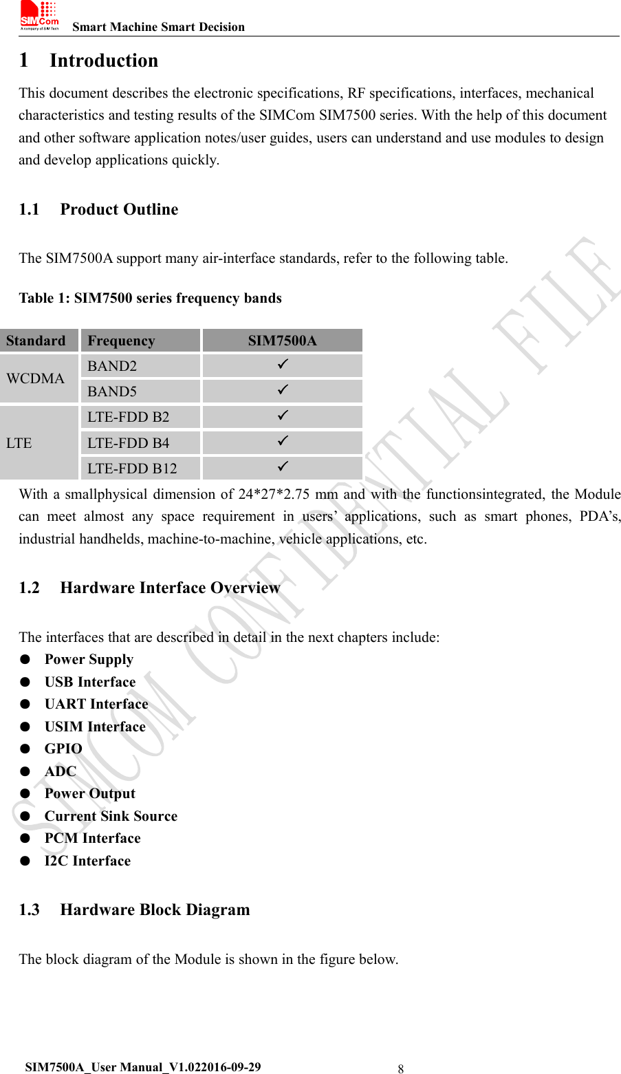
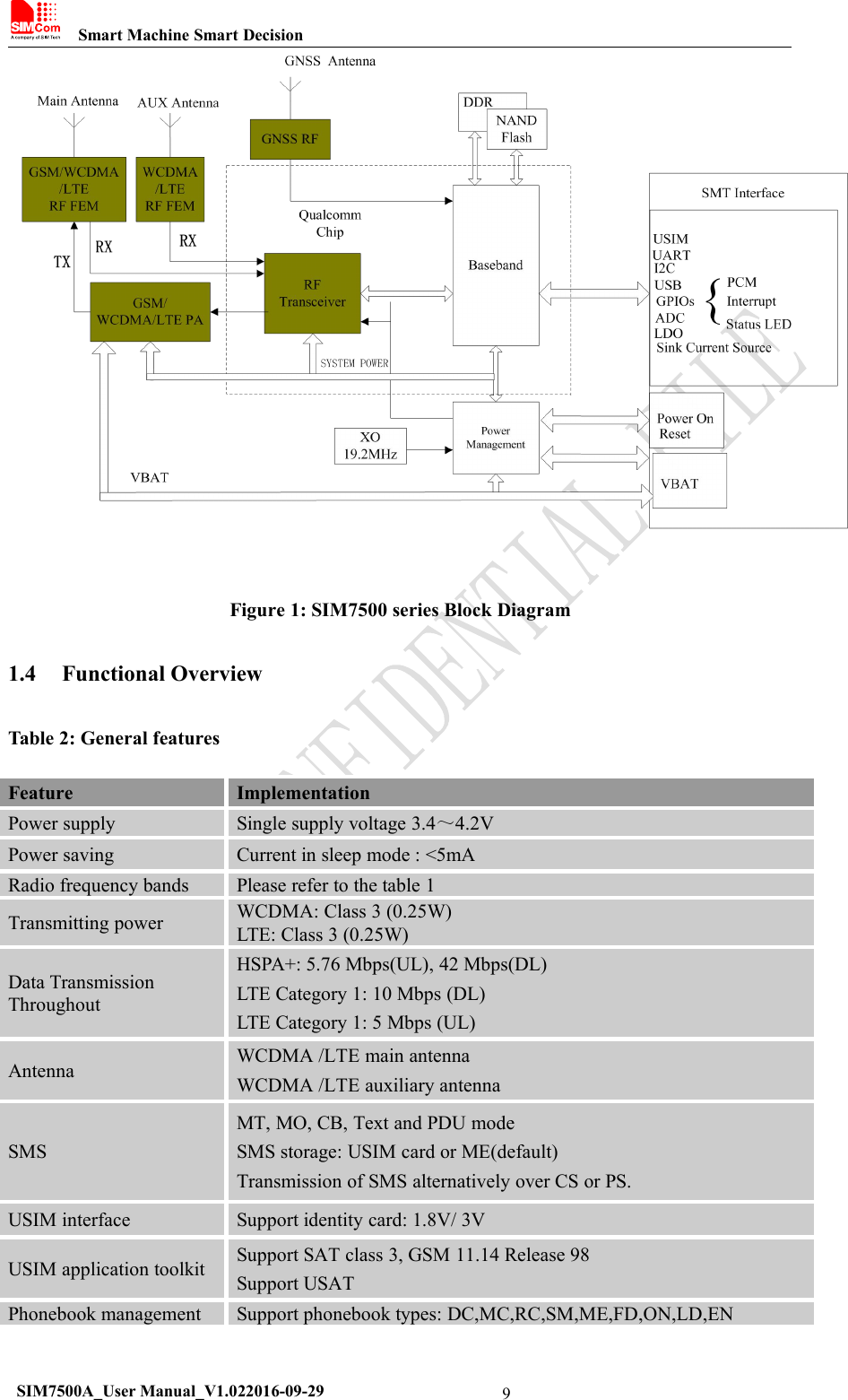
Smart Machine Smart DecisionSIM7500A_User Manual_V1.022016-09-2981IntroductionThis document describes the electronic specifications, RF specifications, interfaces, mechanicalcharacteristics and testing results of the SIMCom SIM7500 series. With the help of this documentand other software application notes/user guides, users can understand and use modules to designand develop applications quickly.1.1 Product OutlineThe SIM7500A support many air-interface standards, refer to the following table.Table 1: SIM7500 series frequency bandsStandardFrequencySIM7500AWCDMABAND2BAND5LTELTE-FDD B2LTE-FDD B4LTE-FDD B12With a smallphysical dimension of 24*27*2.75 mm and with the functionsintegrated, the Modulecan meet almost any space requirement in users’ applications, such as smart phones, PDA’s,industrial handhelds, machine-to-machine, vehicle applications, etc.1.2 Hardware Interface OverviewThe interfaces that are described in detail in the next chapters include:●Power Supply●USB Interface●UART Interface●USIM Interface●GPIO●ADC●Power Output●Current Sink Source●PCM Interface●I2C Interface1.3 Hardware Block DiagramThe block diagram of the Module is shown in the figure below.
Smart Machine Smart DecisionSIM7500A_User Manual_V1.022016-09-299Figure 1: SIM7500 series Block Diagram1.4 Functional OverviewTable 2: General featuresFeatureImplementationPower supplySingle supply voltage 3.4~4.2VPower savingCurrent in sleep mode : <5mARadio frequency bandsPlease refer to the table 1Transmitting powerWCDMA: Class 3 (0.25W)LTE: Class 3 (0.25W)Data TransmissionThroughoutHSPA+: 5.76 Mbps(UL), 42 Mbps(DL)LTE Category 1: 10 Mbps (DL)LTE Category 1: 5 Mbps (UL)AntennaWCDMA /LTE main antennaWCDMA /LTE auxiliary antennaSMSMT, MO, CB, Text and PDU modeSMS storage: USIM card or ME(default)Transmission of SMS alternatively over CS or PS.USIM interfaceSupport identity card: 1.8V/ 3VUSIM application toolkitSupport SAT class 3, GSM 11.14 Release 98Support USATPhonebook managementSupport phonebook types: DC,MC,RC,SM,ME,FD,ON,LD,EN
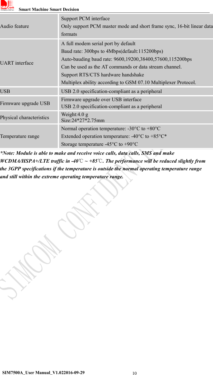
Smart Machine Smart DecisionSIM7500A_User Manual_V1.022016-09-2910Audio featureSupport PCM interfaceOnly support PCM master mode and short frame sync, 16-bit linear dataformatsUART interfaceA full modem serial port by defaultBaud rate: 300bps to 4Mbps(default:115200bps)Auto-bauding baud rate: 9600,19200,38400,57600,115200bpsCan be used as the AT commands or data stream channel.Support RTS/CTS hardware handshakeMultiplex ability according to GSM 07.10 Multiplexer Protocol.USBUSB 2.0 specification-compliant as a peripheralFirmware upgrade USBFirmware upgrade over USB interfaceUSB 2.0 specification-compliant as a peripheralPhysical characteristicsWeight:4.0 gSize:24*27*2.75mmTemperature rangeNormal operation temperature: -30°C to +80°CExtended operation temperature: -40°C to +85°C*Storage temperature -45°C to +90°C*Note: Module is able to make and receive voice calls, data calls, SMS and makeWCDMA/HSPA+/LTE traffic in -40℃~ +85℃. The performance will be reduced slightly fromthe 3GPP specifications if the temperature is outside the normal operating temperature rangeand still within the extreme operating temperature range.
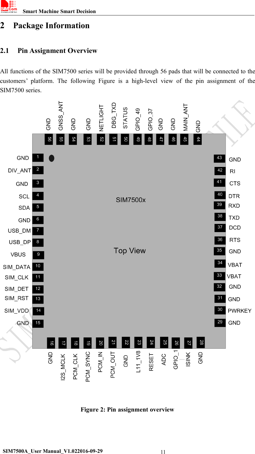
Smart Machine Smart DecisionSIM7500A_User Manual_V1.022016-09-29112Package Information2.1 Pin Assignment OverviewAll functions of the SIM7500 series will be provided through 56 pads that will be connected to thecustomers’ platform. The following Figure is a high-level view of the pin assignment of theSIM7500 series.Figure 2: Pin assignment overview
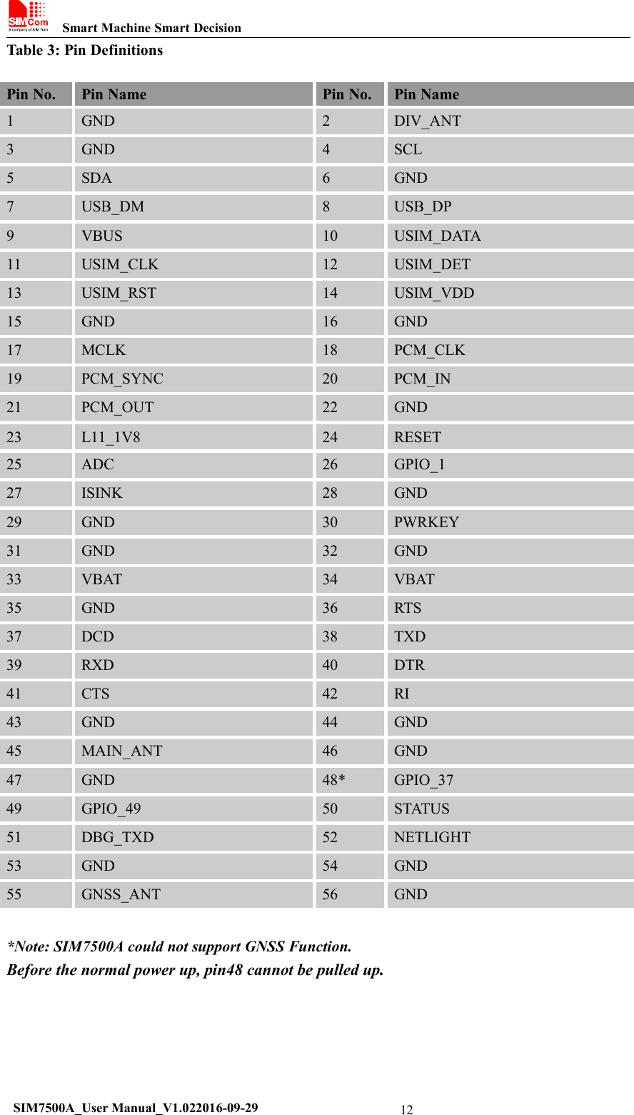
Smart Machine Smart DecisionSIM7500A_User Manual_V1.022016-09-2912Table 3: Pin DefinitionsPin No.Pin NamePin No.Pin Name1GND2DIV_ANT3GND4SCL5SDA6GND7USB_DM8USB_DP9VBUS10USIM_DATA11USIM_CLK12USIM_DET13USIM_RST14USIM_VDD15GND16GND17MCLK18PCM_CLK19PCM_SYNC20PCM_IN21PCM_OUT22GND23L11_1V824RESET25ADC26GPIO_127ISINK28GND29GND30PWRKEY31GND32GND33VBAT34VBAT35GND36RTS37DCD38TXD39RXD40DTR41CTS42RI43GND44GND45MAIN_ANT46GND47GND48*GPIO_3749GPIO_4950STATUS51DBG_TXD52NETLIGHT53GND54GND55GNSS_ANT56GND*Note: SIM7500A could not support GNSS Function.Before the normal power up, pin48 cannot be pulled up.
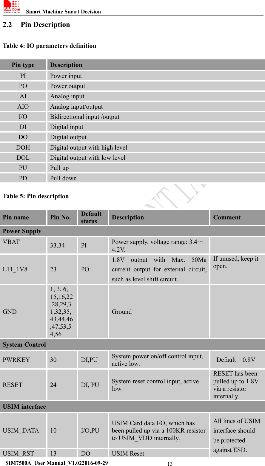
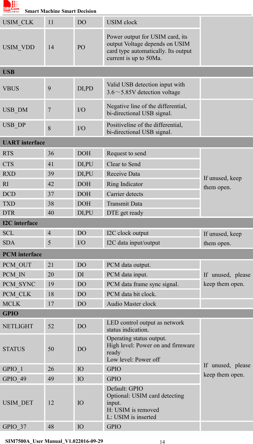
Smart Machine Smart DecisionSIM7500A_User Manual_V1.022016-09-29132.2 Pin DescriptionTable 4: IO parameters definitionPin typeDescriptionPIPower inputPOPower outputAIAnalog inputAIOAnalog input/outputI/OBidirectional input /outputDIDigital inputDODigital outputDOHDigital output with high levelDOLDigital output with low levelPUPull upPDPull downTable 5: Pin descriptionPin namePin No.DefaultstatusDescriptionCommentPower SupplyVBAT33,34PIPower supply, voltage range: 3.4~4.2V.L11_1V823PO1.8V output with Max. 50Macurrent output for external circuit,such as level shift circuit.If unused, keep itopen.GND1, 3, 6,15,16,22,28,29,31,32,35,43,44,46,47,53,54,56GroundSystem ControlPWRKEY30DI,PUSystem power on/off control input,active low.Default 0.8VRESET24DI, PUSystem reset control input, activelow.RESET has beenpulled up to 1.8Vvia a resistorinternally.USIM interfaceUSIM_DATA10I/O,PUUSIM Card data I/O, which hasbeen pulled up via a 100KR resistorto USIM_VDD internally.All lines of USIMinterface shouldbe protectedagainst ESD.USIM_RST13DOUSIM Reset
Smart Machine Smart DecisionSIM7500A_User Manual_V1.022016-09-2914USIM_CLK11DOUSIM clockUSIM_VDD14POPower output for USIM card, itsoutput Voltage depends on USIMcard type automatically. Its outputcurrent is up to 50Ma.USBVBUS9DI,PDValid USB detection input with3.6~5.85V detection voltageUSB_DM7I/ONegative line of the differential,bi-directional USB signal.USB_DP8I/OPositiveline of the differential,bi-directional USB signal.UART interfaceRTS36DOHRequest to sendIf unused, keepthem open.CTS41DI,PUClear to SendRXD39DI,PUReceive DataRI42DOHRing IndicatorDCD37DOHCarrier detectsTXD38DOHTransmit DataDTR40DI,PUDTE get readyI2C interfaceSCL4DOI2C clock outputIf unused, keepthem open.SDA5I/OI2C data input/outputPCM interfacePCM_OUT21DOPCM data output.If unused, pleasekeep them open.PCM_IN20DIPCM data input.PCM_SYNC19DOPCM data frame sync signal.PCM_CLK18DOPCM data bit clock.MCLK17DOAudio Master clockGPIONETLIGHT52DOLED control output as networkstatus indication.If unused, pleasekeep them open.STATUS50DOOperating status output.High level: Power on and firmwarereadyLow level: Power offGPIO_126IOGPIOGPIO_4949IOGPIOUSIM_DET12IODefault: GPIOOptional: USIM card detectinginput.H: USIM is removedL: USIM is insertedGPIO_3748IOGPIO
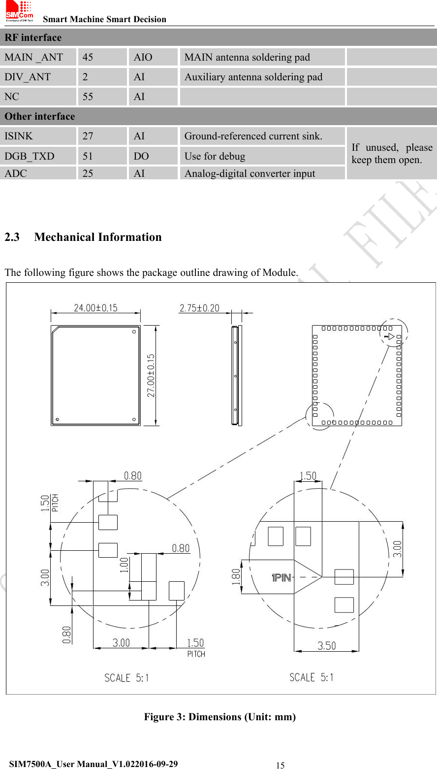
Smart Machine Smart DecisionSIM7500A_User Manual_V1.022016-09-2915RF interfaceMAIN _ANT45AIOMAIN antenna soldering padDIV_ANT2AIAuxiliary antenna soldering padNC55AIOther interfaceISINK27AIGround-referenced current sink.If unused, pleasekeep them open.DGB_TXD51DOUse for debugADC25AIAnalog-digital converter input2.3 Mechanical InformationThe following figure shows the package outline drawing of Module.Figure 3: Dimensions (Unit: mm)
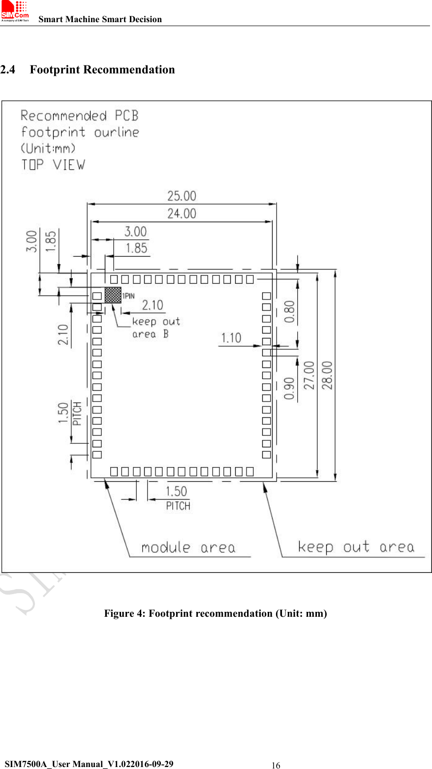
Smart Machine Smart DecisionSIM7500A_User Manual_V1.022016-09-29162.4 Footprint RecommendationFigure 4: Footprint recommendation (Unit: mm)
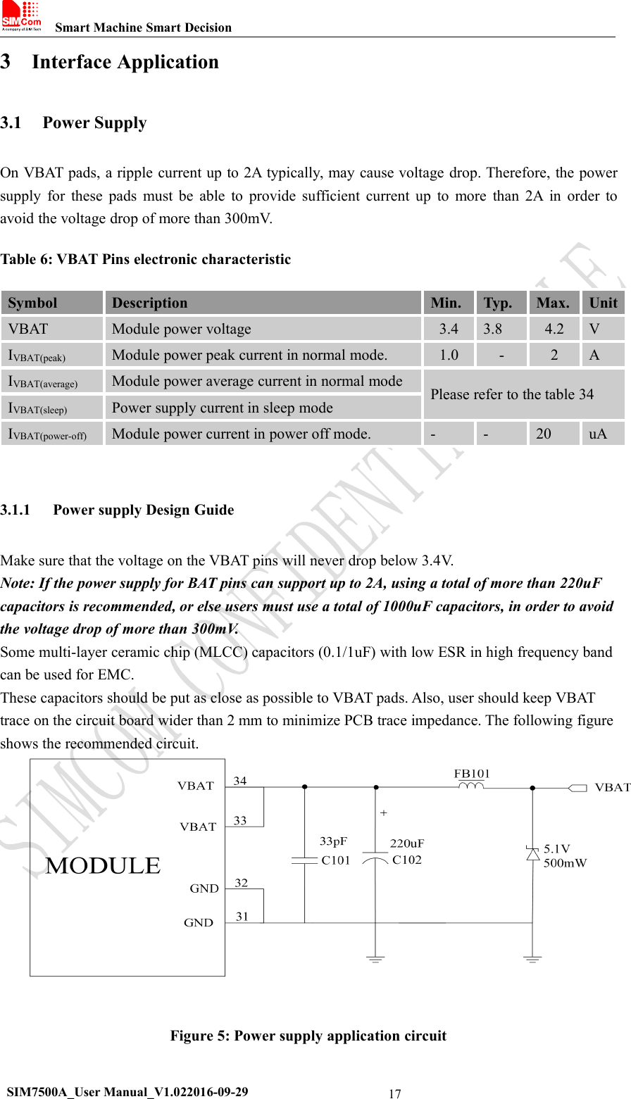
Smart Machine Smart DecisionSIM7500A_User Manual_V1.022016-09-29173Interface Application3.1 Power SupplyOn VBAT pads, a ripple current up to 2A typically, may cause voltage drop. Therefore, the powersupply for these pads must be able to provide sufficient current up to more than 2A in order toavoid the voltage drop of more than 300mV.Table 6: VBAT Pins electronic characteristicSymbolDescriptionMin.Typ.Max.UnitVBATModule power voltage3.43.84.2VIVBAT(peak)Module power peak current in normal mode.1.0-2AIVBAT(average)Module power average current in normal modePlease refer to the table 34IVBAT(sleep)Power supply current in sleep modeIVBAT(power-off)Module power current in power off mode.--20uA3.1.1 Power supply Design GuideMake sure that the voltage on the VBAT pins will never drop below 3.4V.Note: If the power supply for BAT pins can support up to 2A, using a total of more than 220uFcapacitors is recommended, or else users must use a total of 1000uF capacitors, in order to avoidthe voltage drop of more than 300mV.Some multi-layer ceramic chip (MLCC) capacitors (0.1/1uF) with low ESR in high frequency bandcan be used for EMC.These capacitors should be put as close as possible to VBAT pads. Also, user should keep VBATtrace on the circuit board wider than 2 mm to minimize PCB trace impedance. The following figureshows the recommended circuit.Figure 5: Power supply application circuit
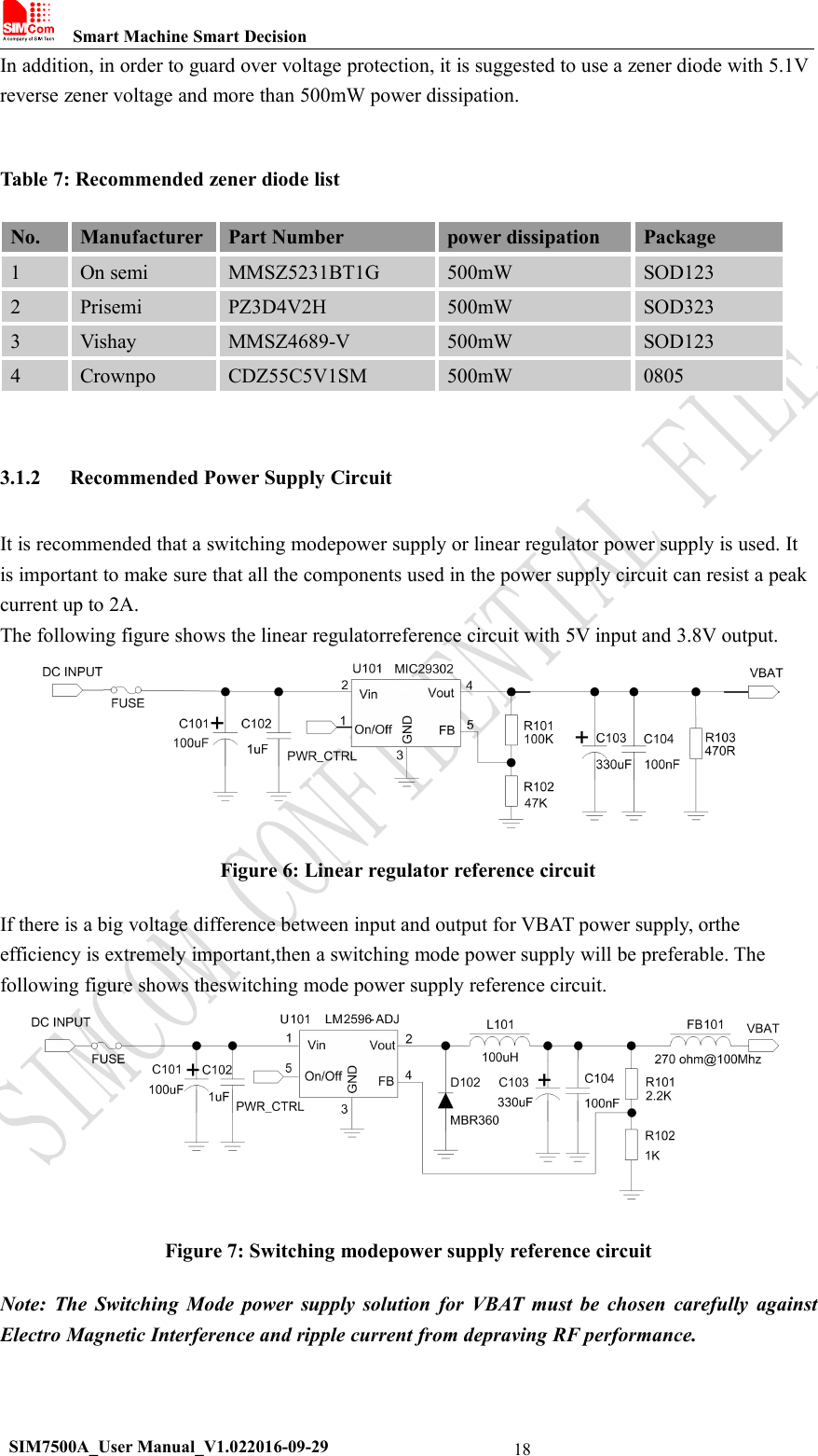
Smart Machine Smart DecisionSIM7500A_User Manual_V1.022016-09-2918In addition, in order to guard over voltage protection, it is suggested to use a zener diode with 5.1Vreverse zener voltage and more than 500mW power dissipation.Table 7: Recommended zener diode listNo.ManufacturerPart Numberpower dissipationPackage1On semiMMSZ5231BT1G500mWSOD1232PrisemiPZ3D4V2H500mWSOD3233VishayMMSZ4689-V500mWSOD1234CrownpoCDZ55C5V1SM500mW08053.1.2 Recommended Power Supply CircuitIt is recommended that a switching modepower supply or linear regulator power supply is used. Itis important to make sure that all the components used in the power supply circuit can resist a peakcurrent up to 2A.The following figure shows the linear regulatorreference circuit with 5V input and 3.8V output.Figure 6: Linear regulator reference circuitIf there is a big voltage difference between input and output for VBAT power supply, ortheefficiency is extremely important,then a switching mode power supply will be preferable. Thefollowing figure shows theswitching mode power supply reference circuit.Figure 7: Switching modepower supply reference circuitNote: The Switching Mode power supply solution for VBAT must be chosen carefully againstElectro Magnetic Interference and ripple current from depraving RF performance.
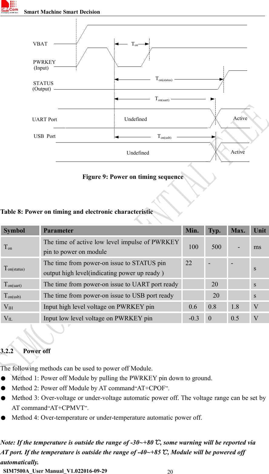
Smart Machine Smart DecisionSIM7500A_User Manual_V1.022016-09-29193.1.3 Voltage MonitorTo monitor the VBAT voltage, the AT command “AT+CBC” can be used.For monitoring the VBAT voltage outside or within a special range, the AT command“AT+CVALARM” can be used to enable the under-voltage warning function.If users need to power off Module, when the VBAT voltage is out of a range, the AT command“AT+CPMVT” can be used to enable under-voltage power-off function.Note: Under-voltage warning function and under-voltage power-off function are disabled bydefault. For more information about these AT commands, please refer to Document [1].3.2 Power on/Power off/Reset Function3.2.1 Power onModule can be powered on by pulling the PWRKEY pin down to ground.The PWRKEY pin has been pulled up to dVDDinternally, so you does not need to pull it upexternally. It is strongly recommended to put a100nF capacitor and an ESD protection diode closeto the PWRKEY pin. Please refer to the following figure for the recommended reference circuit.47KPWRKEY PowerOn off logicDiodedVDDMODULE100Ω100nF4.7KTurn on /offimpulseFigure 8: ReferencePower on/offCircuitThe power-on scenarios are illustrated in the following figure.
Smart Machine Smart DecisionSIM7500A_User Manual_V1.022016-09-2920STATUS(Output)TonVBATPWRKEY(Input)Ton(status)UART Port Undefined ActiveTon(uart)Undefined ActiveUSB  Port Ton(usb)Figure 9: Power on timing sequenceTable 8: Power on timing and electronic characteristicSymbolParameterMin.Typ.Max.UnitTonThe time of active low level impulse of PWRKEYpin to power on module100500-msTon(status)The time from power-on issue to STATUS pinoutput high level(indicating power up ready )22--sTon(uart)The time from power-on issue to UART port ready20sTon(usb)The time from power-on issue to USB port ready20sVIHInput high level voltage on PWRKEY pin0.60.81.8VVILInput low level voltage on PWRKEY pin-0.300.5V3.2.2 Power offThe following methods can be used to power off Module.●Method 1: Power off Module by pulling the PWRKEY pin down to ground.●Method 2: Power off Module by AT command“AT+CPOF”.●Method 3: Over-voltage or under-voltage automatic power off. The voltage range can be set byAT command“AT+CPMVT”.●Method 4: Over-temperature or under-temperature automatic power off.Note: If the temperature is outside the range of -30~+80℃, some warning will be reported viaAT port. If the temperature is outside the range of -40~+85℃, Module will be powered offautomatically.
Smart Machine Smart DecisionSIM7500A_User Manual_V1.022016-09-2921For details about “AT+CPOF” and “AT+CPMVT”, please refer to Document [1].These procedures will make modules disconnect from the network and allow the software to enter asafe state and save data before modules are powered off completely.The power off scenario by pulling down the PWRKEY pin is illustrated in the following figure.(Output )Toff( Input )Toff(status)UART Port UndefinedActiveToff(uart)TonToff-onUSB Port UndefinedActiveToff(usb)PWRKEYSTATUSFigure 10: Power off timing sequenceTable 9: Power off timing and Electronic CharacteristicSymbolParameterTime valueUnitMin.Typ.Max.ToffThe active low level time pulse on PWRKEY pin topower off module2.5----sToff(status)The time from power-off issue to STATUS pin outputlow level(indicating power off )*22--sToff(uart)The time from power-off issue to UART port off15--sToff(usb)The time from power-off issue to USB port off15--sToff-onThe buffer time from power-off issue to power-onissue0--s3.2.3 Reset FunctionModule can be reset by pulling the RESET pin down to ground.Note: This function is only used as an emergency reset when AT command “AT+CPOF” and thePWRKEY pin all have lost efficacy.
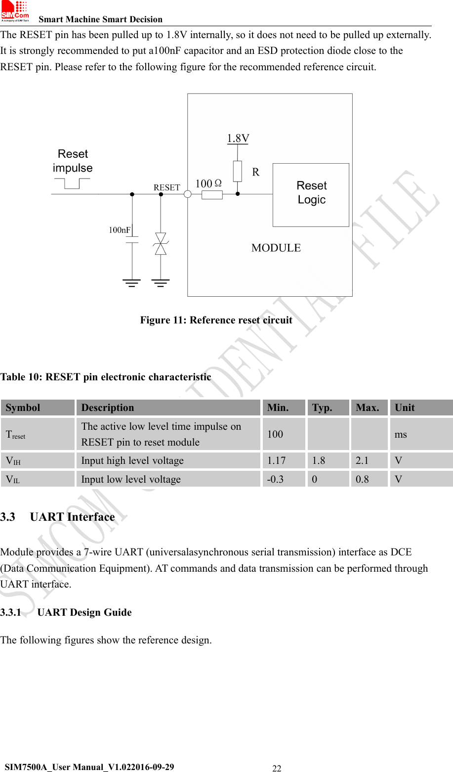
Smart Machine Smart DecisionSIM7500A_User Manual_V1.022016-09-2922The RESET pin has been pulled up to 1.8V internally, so it does not need to be pulled up externally.It is strongly recommended to put a100nF capacitor and an ESD protection diode close to theRESET pin. Please refer to the following figure for the recommended reference circuit.Figure 11: Reference reset circuitTable 10: RESET pin electronic characteristicSymbolDescriptionMin.Typ.Max.UnitTresetThe active low level time impulse onRESET pin to reset module100msVIHInput high level voltage1.171.82.1VVILInput low level voltage-0.300.8V3.3 UART InterfaceModule provides a 7-wire UART (universalasynchronous serial transmission) interface as DCE(Data Communication Equipment). AT commands and data transmission can be performed throughUART interface.3.3.1 UART Design GuideThe following figures show the reference design.
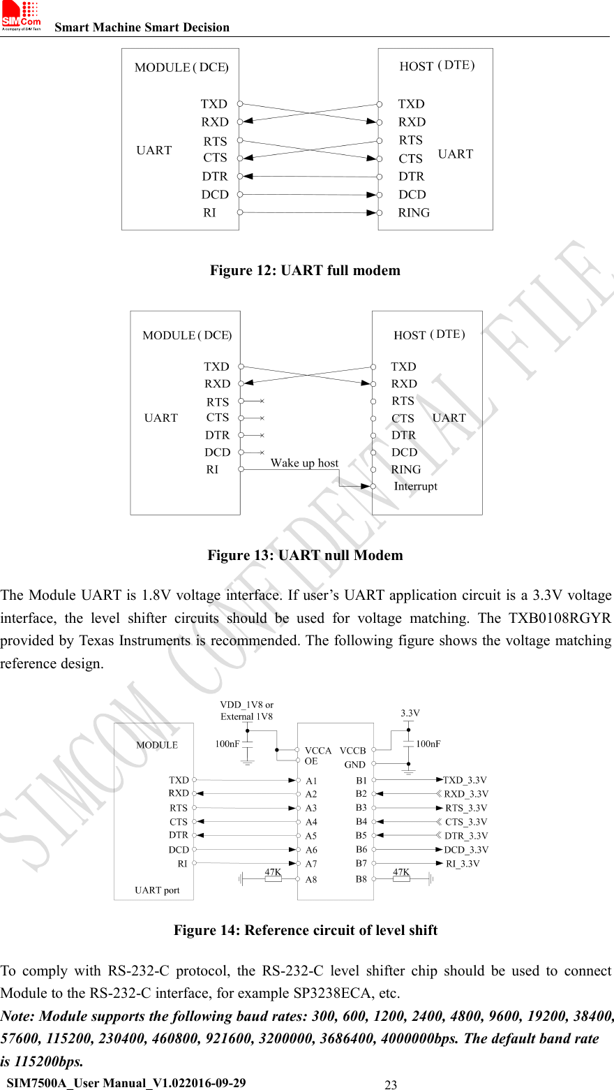
Smart Machine Smart DecisionSIM7500A_User Manual_V1.022016-09-2923Figure 12: UART full modemFigure 13: UART null ModemThe Module UART is 1.8V voltage interface. If user’s UART application circuit is a 3.3V voltageinterface, the level shifter circuits should be used for voltage matching. The TXB0108RGYRprovided by Texas Instruments is recommended. The following figure shows the voltage matchingreference design.Figure 14: Reference circuit of level shiftTo comply with RS-232-C protocol, the RS-232-C level shifter chip should be used to connectModule to the RS-232-C interface, for example SP3238ECA, etc.Note: Module supports the following baud rates: 300, 600, 1200, 2400, 4800, 9600, 19200, 38400,57600, 115200, 230400, 460800, 921600, 3200000, 3686400, 4000000bps. The default band rateis 115200bps.
Smart Machine Smart DecisionSIM7500A_User Manual_V1.022016-09-29243.3.2 RI and DTR BehaviorThe RI pin can be used to interrupt output signal to inform the host controller such as applicationCPU.Normally RI will stay at high level until certain conditions such as receiving SMS, or a URC reportcome in. It will then change to low level. It will stay low until the host controller clears theinterrupted event with “AT+CRIRS” AT command.Figure 15: RI behaviour(SMS and URC report)Normally RI will be kept high until a voice call, then it will output periodic rectangular wave with5900ms low level and 100ms high level. It will output this kind of periodic rectangular wave untilthe call is answered or hung up.Figure 16: RI behaviour(voice call)Note: For more details of AT commands about UART, please refer to document [1] and [22].DTR pin can be used to wake Module from sleep. When Module enters sleep mode, pulling downDTR can wake Module.3.4 USB InterfaceThe Module contains a USB interface compliant with the USB2.0 specification as a peripheral, butthe USB charging function is not supported.
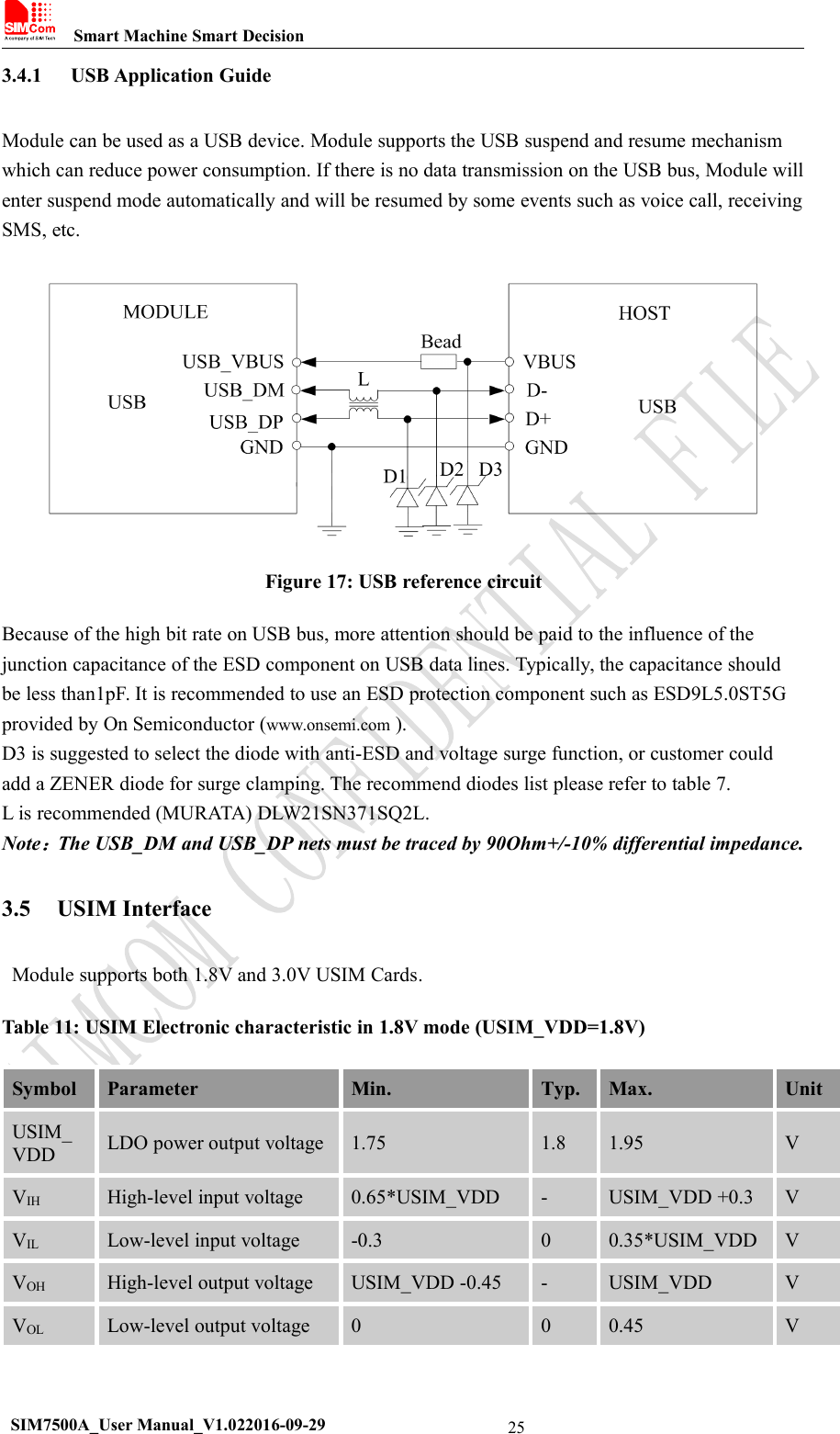
Smart Machine Smart DecisionSIM7500A_User Manual_V1.022016-09-29253.4.1 USB Application GuideModule can be used as a USB device. Module supports the USB suspend and resume mechanismwhich can reduce power consumption. If there is no data transmission on the USB bus, Module willenter suspend mode automatically and will be resumed by some events such as voice call, receivingSMS, etc.Figure 17: USB reference circuitBecause of the high bit rate on USB bus, more attention should be paid to the influence of thejunction capacitance of the ESD component on USB data lines. Typically, the capacitance shouldbe less than1pF. It is recommended to use an ESD protection component such as ESD9L5.0ST5Gprovided by On Semiconductor (www.onsemi.com ).D3 is suggested to select the diode with anti-ESD and voltage surge function, or customer couldadd a ZENER diode for surge clamping. The recommend diodes list please refer to table 7.L is recommended (MURATA) DLW21SN371SQ2L.Note:The USB_DM and USB_DP nets must be traced by 90Ohm+/-10% differential impedance.3.5 USIM InterfaceModule supports both 1.8V and 3.0V USIM Cards.Table 11: USIM Electronic characteristic in 1.8V mode (USIM_VDD=1.8V)SymbolParameterMin.Typ.Max.UnitUSIM_VDDLDO power output voltage1.751.81.95VVIHHigh-level input voltage0.65*USIM_VDD-USIM_VDD +0.3VVILLow-level input voltage-0.300.35*USIM_VDDVVOHHigh-level output voltageUSIM_VDD -0.45-USIM_VDDVVOLLow-level output voltage000.45V
Smart Machine Smart DecisionSIM7500A_User Manual_V1.022016-09-2926Table 12: USIM Electronic characteristic 3.0V mode (USIM_VDD=2.95V)SymbolParameterMin.Typ.Max.UnitUSIM_VDDLDO power output voltage2.752.953.05VVIHHigh-level input voltage0.65*USIM_VDD-USIM_VDD +0.3VVILLow-level input voltage-0.300.25*USIM_VDDVVOHHigh-level output voltageUSIM_VDD -0.45-USIM_VDDVVOLLow-level output voltage000.45V3.5.1 USIM Application GuideIt is recommended to use an ESD protection component such as ESDA6V1W5 produced by ST(www.st.com ) or SMF15C produced by ON SEMI (www.onsemi.com ). Note that the USIMperipheral circuit should be close to the USIM card socket.The following figure shows the 6-pinSIM card holder reference circuit.Figure 18: USIM interface reference circuitNote: USIM_DATA has been pulled up with a100KΩ resistor to USIM_VDD in module. A 100nFcapacitor on USIM_VDD is used to reduceinterference. For more details of AT commands aboutUSIM, please refer to document [1].3.5.2 SIM Card Design GuideSIM card signal could be interferenced by some high frequency signal, it is strongly recommendedto follow these guidelines while designing:SIM card holder should be far away from antennaSIM traces should keep away from RF lines, VBAT and high-speed signal linesThe traces should be as short as possibleKeep SIM card holder’s GND connect to main ground directly
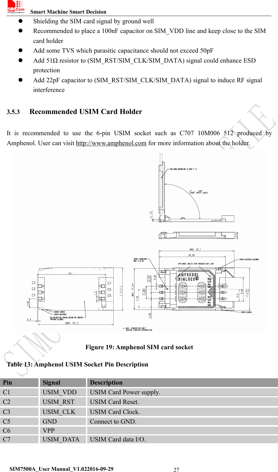
Smart Machine Smart DecisionSIM7500A_User Manual_V1.022016-09-2927Shielding the SIM card signal by ground wellRecommended to place a 100nF capacitor on SIM_VDD line and keep close to the SIMcard holderAdd some TVS which parasitic capacitance should not exceed 50pFAdd 51Ω resistor to (SIM_RST/SIM_CLK/SIM_DATA) signal could enhance ESDprotectionAdd 22pF capacitor to (SIM_RST/SIM_CLK/SIM_DATA) signal to induce RF signalinterference3.5.3 Recommended USIM Card HolderIt is recommended to use the 6-pin USIM socket such as C707 10M006 512 produced byAmphenol. User can visit http://www.amphenol.com for more information about the holder.Figure 19: Amphenol SIM card socketTable 13: Amphenol USIM Socket Pin DescriptionPinSignalDescriptionC1USIM_VDDUSIM Card Power supply.C2USIM_RSTUSIM Card Reset.C3USIM_CLKUSIM Card Clock.C5GNDConnect to GND.C6VPPC7USIM_DATAUSIM Card data I/O.
Smart Machine Smart DecisionSIM7500A_User Manual_V1.022016-09-29283.6 PCM InterfaceModule provides a PCM interface for external codec, which can be used inmaster mode with shortsync and 16 bits linear format.Table 14: PCM FormatNote: For more details about PCM AT commands, please refer to document [1].3.6.1 PCM TimingModule supports 2.048 MHz PCM data and sync timing for 16 bits linear format codec.Figure 20: PCM_SYNC timingFigure 21: EXT codec to module timingCharacteristicsSpecificationLineInterfaceFormatLinear(Fixed)Datalength16bits(Fixed)PCM Clock/Sync SourceMaster Mode(Fixed)PCMClockRate2048 KHz (Fixed)PCMSyncFormatShortsync(Fixed)Data OrderingMSB
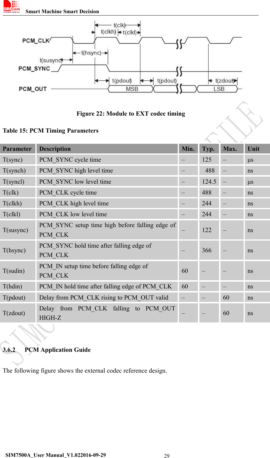
Smart Machine Smart DecisionSIM7500A_User Manual_V1.022016-09-2929Figure 22: Module to EXT codec timingTable 15: PCM Timing ParametersParameterDescriptionMin.Typ.Max.UnitT(sync)PCM_SYNC cycle time–125–μsT(synch)PCM_SYNC high level time–488–nsT(syncl)PCM_SYNC low level time–124.5–μsT(clk)PCM_CLK cycle time–488–nsT(clkh)PCM_CLK high level time–244–nsT(clkl)PCM_CLK low level time–244–nsT(susync)PCM_SYNC setup time high before falling edge ofPCM_CLK–122–nsT(hsync)PCM_SYNC hold time after falling edge ofPCM_CLK–366–nsT(sudin)PCM_IN setup time before falling edge ofPCM_CLK60––nsT(hdin)PCM_IN hold time after falling edge of PCM_CLK60––nsT(pdout)Delay from PCM_CLK rising to PCM_OUT valid––60nsT(zdout)Delay from PCM_CLK falling to PCM_OUTHIGH-Z––60ns3.6.2 PCM Application GuideThe following figure shows the external codec reference design.
Smart Machine Smart DecisionSIM7500A_User Manual_V1.022016-09-2930Figure 23: Audio codec reference circuitNote: Module can transmit PCM data by theUSB portbesidesthe PCM interface. For moredetails please refer to documents [1] and [23].3.7 I2C InterfaceModule provides a I2C interface compatible with I2C specification, version 2.1, with clock rate upto 400 kbps. Its operation voltage is 1.8V.3.7.1 I2C Design GuideThe following figure shows the I2C bus reference design.Figure 24: I2C reference circuitNote:SDA and SCLhave pull-up resistors in module. So, 2 external pull up resistors are not needed inapplication circuit.“AT+CRIIC and AT+CWIIC” AT commands could be used to read/write register values of theI2C peripheral devices.For more details about AT commands please refer to document [1].
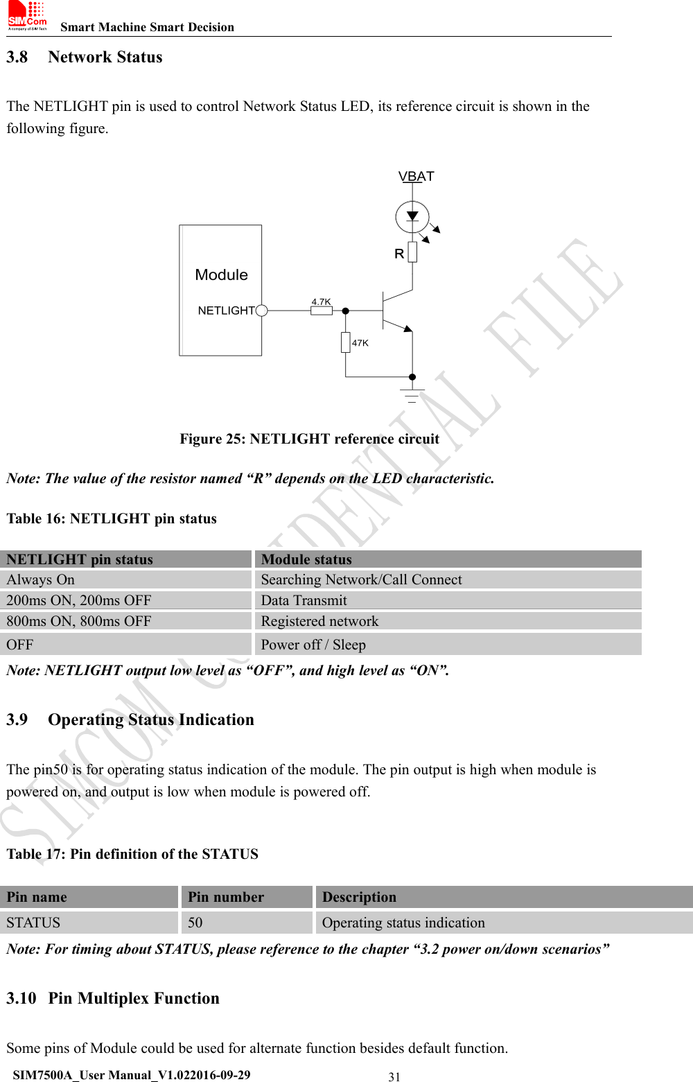
Smart Machine Smart DecisionSIM7500A_User Manual_V1.022016-09-29313.8 Network StatusThe NETLIGHT pin is used to control Network Status LED, its reference circuit is shown in thefollowing figure.Figure 25: NETLIGHT reference circuitNote: The value of the resistor named “R” depends on the LED characteristic.Table 16: NETLIGHT pin statusNETLIGHT pin statusModule statusAlways OnSearching Network/Call Connect200ms ON, 200ms OFFData Transmit800ms ON, 800ms OFFRegistered networkOFFPower off / SleepNote: NETLIGHT output low level as “OFF”, and high level as “ON”.3.9 Operating Status IndicationThe pin50 is for operating status indication of the module. The pin output is high when module ispowered on, and output is low when module is powered off.Table 17: Pin definition of the STATUSPin namePin numberDescriptionSTATUS50Operating status indicationNote: For timing about STATUS, please reference to the chapter “3.2 power on/down scenarios”3.10 Pin Multiplex FunctionSome pins of Module could be used for alternate function besides default function.
Smart Machine Smart DecisionSIM7500A_User Manual_V1.022016-09-2932Table 18: Pin multiplex function listNote:For more details of AT commands about GPIO multiplex function,please refer todocument [1].3.11 Other interface3.11.1 Sink Current SourceThe ISINK pin is VBATtolerant and intended to drive some passive devices such as LCD backlight,white LED, etc. Its output current can be up to 40 mA and be set by the AT command “AT+CLEDITST”.Table 19: Sink current electronic characteristicSymbolDescriptionMin.Typ.Max.UnitVISINKVoltage tolerant0.5-VBATVIISINKCurrent tolerant0-40mAISINK is a ground-referenced current sink. The following figure shows its reference circuit.Figure 26: ISINK reference circuitPin NumberPin NameDefault FunctionAlternate Function4SCLSCLGPIO115SDASDAGPIO1012USIM_DETGPIO34USIM_DET18PCM_CLKPCM_CLKGPIO23,SPI_CLKI2C_SCL19PCM_SYNCPCM_SYNCGPIO20,SPI_MOSI20PCM_INPCM_IN,GPIO21,SPI_MISO21PCM_OUTPCM_OUTGPIO22,SPI_CS_NI2C_SDA
Smart Machine Smart DecisionSIM7500A_User Manual_V1.022016-09-2933Note: The sinking current can be adjusted to meet the design requirement through the ATcommand “AT+ CLEDITST =<0>, <value>”.The “value” ranges from 0 to 8, on behalf of thecurrent from 0mA to 40mA by 5mA step.3.11.2 ADCModule has 1 dedicated ADC pins named ADC. They are available fordigitizing analog signalssuch as battery voltage and so on. These electronic specifications are shown in the following table.Table 20: ADC Electronic CharacteristicsCharacteristicsMin.Typ.Max.UnitResolution–15–BitsInput Range0.11.7VInput serial resistance1––MΩNote: “AT+CADC” can be used to read the voltage of the ADC pins, for more details, pleaserefer to document [1].
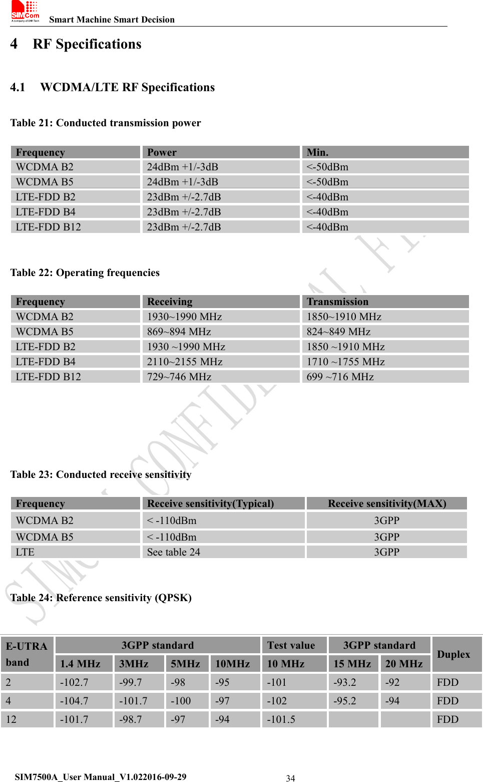
Smart Machine Smart DecisionSIM7500A_User Manual_V1.022016-09-29344RF Specifications4.1 WCDMA/LTE RF SpecificationsTable 21: Conducted transmission powerFrequencyPowerMin.WCDMA B224dBm +1/-3dB<-50dBmWCDMA B524dBm +1/-3dB<-50dBmLTE-FDD B223dBm +/-2.7dB<-40dBmLTE-FDD B423dBm +/-2.7dB<-40dBmLTE-FDD B1223dBm +/-2.7dB<-40dBmTable 22: Operating frequenciesFrequencyReceivingTransmissionWCDMA B21930~1990 MHz1850~1910 MHzWCDMA B5869~894 MHz824~849 MHzLTE-FDD B21930 ~1990 MHz1850 ~1910 MHzLTE-FDD B42110~2155 MHz1710 ~1755 MHzLTE-FDD B12729~746 MHz699 ~716 MHzTable 23: Conducted receive sensitivityFrequencyReceive sensitivity(Typical)Receive sensitivity(MAX)WCDMA B2< -110dBm3GPPWCDMA B5< -110dBm3GPPLTESee table 243GPPTable 24: Reference sensitivity (QPSK)E-UTRAband3GPP standardTest value3GPP standardDuplex1.4 MHz3MHz5MHz10MHz10 MHz15 MHz20 MHz2-102.7-99.7-98-95-101-93.2-92FDD4-104.7-101.7-100-97-102-95.2-94FDD12-101.7-98.7-97-94-101.5FDD
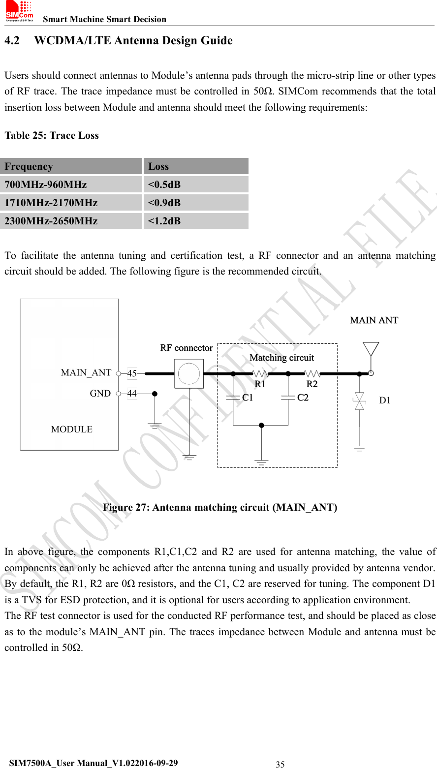
Smart Machine Smart DecisionSIM7500A_User Manual_V1.022016-09-29354.2 WCDMA/LTE Antenna Design GuideUsers should connect antennas to Module’s antenna pads through the micro-strip line or other typesof RF trace. The trace impedance must be controlled in 50Ω. SIMCom recommends that the totalinsertion loss between Module and antenna should meet the following requirements:Table 25: Trace LossFrequencyLoss700MHz-960MHz<0.5dB1710MHz-2170MHz<0.9dB2300MHz-2650MHz<1.2dBTo facilitate the antenna tuning and certification test, a RF connector and an antenna matchingcircuit should be added. The following figure is the recommended circuit.Figure 27: Antenna matching circuit (MAIN_ANT)In above figure, the components R1,C1,C2 and R2 are used for antenna matching, the value ofcomponents can only be achieved after the antenna tuning and usually provided by antenna vendor.By default, the R1, R2 are 0Ω resistors, and the C1, C2 are reserved for tuning. The component D1is a TVS for ESD protection, and it is optional for users according to application environment.The RF test connector is used for the conducted RF performance test, and should be placed as closeas to the module’s MAIN_ANT pin. The traces impedance between Module and antenna must becontrolled in 50Ω.
Smart Machine Smart DecisionSIM7500A_User Manual_V1.022016-09-2936Figure 28: Antenna matching circuit (DIV_ANT)In above figure, R3, C3, C4 and R4 are used for auxiliary antenna matching. By default, the R3, R4are 0Ωresistors, and the C3, C4 are reserved for tuning. D2 is a TVS for ESD protection, and it isoptional for users according to application environment.Two TVS are recommended in the table below.Table 26: Recommended TVSPackagePart NumberVender0201LXES03AAA1-154Murata0402LXES15AAA1-153MurataNote:SIMCom suggests the LTE auxiliary antenna to be kept on, since there are many highbands in the designing of FDD-LTE. Because of the high insert loss of the RF cable and layoutlines, the receiver sensitivity of these bands above will have risk to meet the authenticationwithout the diversity antenna.For more details about auxiliary antenna design notice,pleaserefer to document [25]
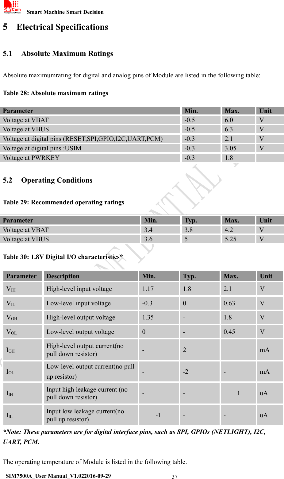
Smart Machine Smart DecisionSIM7500A_User Manual_V1.022016-09-29375Electrical Specifications5.1 Absolute Maximum RatingsAbsolute maximumrating for digital and analog pins of Module are listed in the following table:Table 28: Absolute maximum ratingsParameterMin.Max.UnitVoltage at VBAT-0.56.0VVoltage at VBUS-0.56.3VVoltage at digital pins (RESET,SPI,GPIO,I2C,UART,PCM)-0.32.1VVoltage at digital pins :USIM-0.33.05VVoltage at PWRKEY-0.31.85.2 Operating ConditionsTable 29: Recommended operating ratingsParameterMin.Typ.Max.UnitVoltage at VBAT3.43.84.2VVoltage at VBUS3.655.25VTable 30: 1.8V Digital I/O characteristics*ParameterDescriptionMin.Typ.Max.UnitVIHHigh-level input voltage1.171.82.1VVILLow-level input voltage-0.300.63VVOHHigh-level output voltage1.35-1.8VVOLLow-level output voltage0-0.45VIOHHigh-level output current(nopull down resistor)-2mAIOLLow-level output current(no pullup resistor)--2-mAIIHInput high leakage current (nopull down resistor)--1uAIILInput low leakage current(nopull up resistor)-1--uA*Note: These parameters are for digital interface pins, such as SPI, GPIOs (NETLIGHT), I2C,UART, PCM.The operating temperature of Module is listed in the following table.
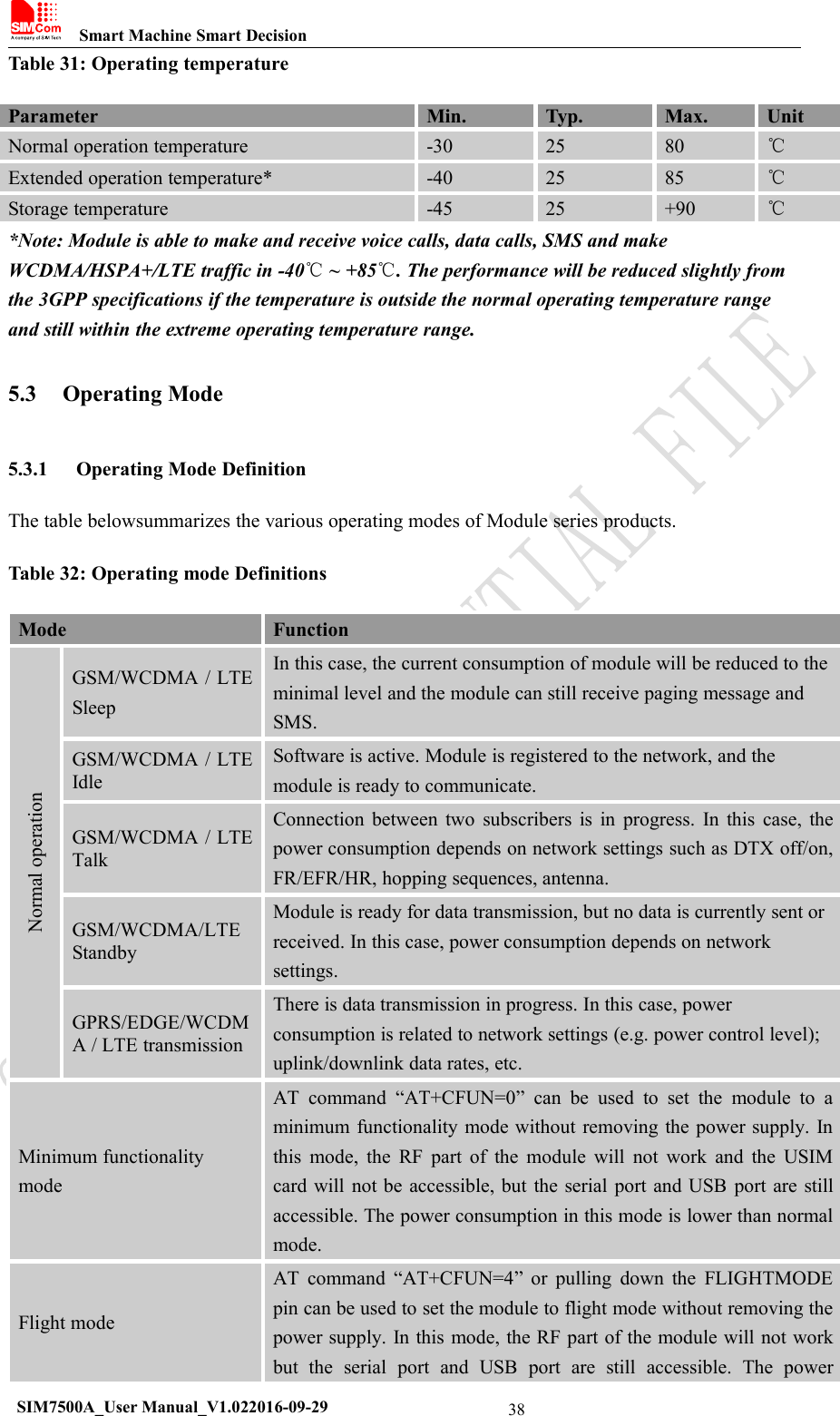
Smart Machine Smart DecisionSIM7500A_User Manual_V1.022016-09-2938Table 31: Operating temperatureParameterMin.Typ.Max.UnitNormal operation temperature-302580℃Extended operation temperature*-402585℃Storage temperature-4525+90℃*Note: Module is able to make and receive voice calls, data calls, SMS and makeWCDMA/HSPA+/LTE traffic in -40℃~ +85℃. The performance will be reduced slightly fromthe 3GPP specifications if the temperature is outside the normal operating temperature rangeand still within the extreme operating temperature range.5.3 Operating Mode5.3.1 Operating Mode DefinitionThe table belowsummarizes the various operating modes of Module series products.Table 32: Operating mode DefinitionsModeFunctionNormal operationGSM/WCDMA / LTESleepIn this case, the current consumption of module will be reduced to theminimal level and the module can still receive paging message andSMS.GSM/WCDMA / LTEIdleSoftware is active. Module is registered to the network, and themodule is ready to communicate.GSM/WCDMA / LTETalkConnection between two subscribers is in progress. In this case, thepower consumption depends on network settings such as DTX off/on,FR/EFR/HR, hopping sequences, antenna.GSM/WCDMA/LTEStandbyModule is ready for data transmission, but no data is currently sent orreceived. In this case, power consumption depends on networksettings.GPRS/EDGE/WCDMA / LTE transmissionThere is data transmission in progress. In this case, powerconsumption is related to network settings (e.g. power control level);uplink/downlink data rates, etc.Minimum functionalitymodeAT command “AT+CFUN=0” can be used to set the module to aminimum functionality mode without removing the power supply. Inthis mode, the RF part of the module will not work and the USIMcard will not be accessible, but the serial port and USB port are stillaccessible. The power consumption in this mode is lower than normalmode.Flight modeAT command “AT+CFUN=4” or pulling down the FLIGHTMODEpin can be used to set the module to flight mode without removing thepower supply. In this mode, the RF part of the module will not workbut the serial port and USB port are still accessible. The power
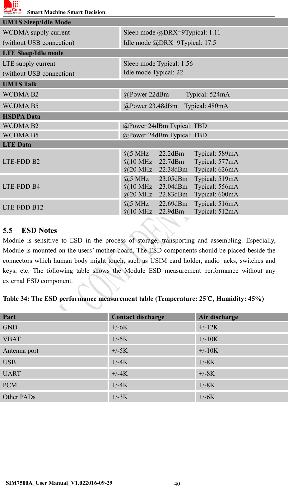
Smart Machine Smart DecisionSIM7500A_User Manual_V1.022016-09-2939consumption in this mode is lower than normal mode.Power offModule will go into power off mode by sending the AT command“AT+CPOF” or by pulling down the PWRKEY pin normally. In thismode the power management unit shuts down the power supply andsoftware is not active. The serial port and USB are is not accessible.5.3.2 Sleep ModeIn sleep mode, the current consumption of module will be reduced to the minimal level, andmodule can still receive paging message and SMS.Several hardware and software conditions must be satisfied together in order to let Module enterinto sleep mode:1. UART condition2. USB condition3. Software conditionNote: Before designing, pay attention to how to realize sleeping/waking function and refer toDocument [26] for more details.5.3.3 Minimum Functionality Mode and Flight ModeMinimum functionality mode ceasesa majority functionof module, thus minimizing the powerconsumption. This mode is set by the AT command which provides a choice of the functionalitylevels.●AT+CFUN=0: Minimum functionality●AT+CFUN=1: Full functionality (Default)●AT+CFUN=4: Flight modeIf Module has been set to minimum functionality mode, the RF function and USIM card functionwill be closed. In this case, the serial port and USB are still accessible, but RF function and USIMcard will be unavailable.If Module has been set to flight mode, the RF function will be closed. In this case, the serial portand USB are still accessible, but RF function will be unavailable.When Module is in minimum functionality or flight mode, it can return to full functionality by theAT command “AT+CFUN=1”.5.4 Current ConsumptionThe current consumption is listed in the table below.Table 33: Current consumption on VBAT Pins (VBAT=3.8V)
Smart Machine Smart DecisionSIM7500A_User Manual_V1.022016-09-2940UMTS Sleep/Idle ModeWCDMA supply current(without USB connection)Sleep mode @DRX=9Typical: 1.11Idle mode @DRX=9Typical: 17.5LTE Sleep/Idle modeLTE supply current(without USB connection)Sleep mode Typical: 1.56Idle mode Typical: 22UMTS TalkWCDMA B2@Power 22dBm Typical: 524mAWCDMA B5@Power 23.48dBm Typical: 480mAHSDPA DataWCDMA B2@Power 24dBm Typical: TBDWCDMA B5@Power 24dBm Typical: TBDLTE DataLTE-FDD B2@5 MHz 22.2dBm Typical: 589mA@10 MHz 22.7dBm Typical: 577mA@20 MHz 22.38dBm Typical: 626mALTE-FDD B4@5 MHz 23.05dBm Typical: 519mA@10 MHz 23.04dBm Typical: 556mA@20 MHz 22.83dBm Typical: 600mALTE-FDD B12@5 MHz 22.69dBm Typical: 516mA@10 MHz 22.9dBm Typical: 512mA5.5 ESD NotesModule is sensitive to ESD in the process of storage, transporting and assembling. Especially,Module is mounted on the users’ mother board, The ESD components should be placed beside theconnectors which human body might touch, such as USIM card holder, audio jacks, switches andkeys, etc. The following table shows the Module ESD measurement performance without anyexternal ESD component.Table 34: The ESD performance measurement table (Temperature: 25℃, Humidity: 45%)PartContact dischargeAir dischargeGND+/-6K+/-12KVBAT+/-5K+/-10KAntenna port+/-5K+/-10KUSB+/-4K+/-8KUART+/-4K+/-8KPCM+/-4K+/-8KOther PADs+/-3K+/-6K
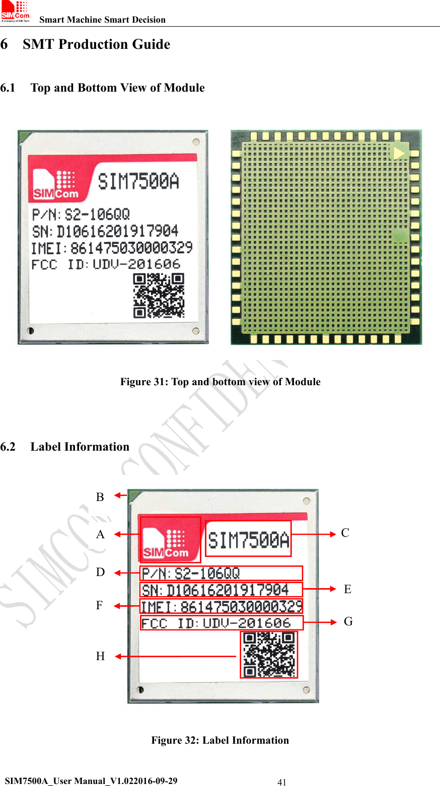
Smart Machine Smart DecisionSIM7500A_User Manual_V1.022016-09-29416SMT Production Guide6.1 Top and Bottom View of ModuleFigure 31: Top and bottom view of Module6.2 Label InformationFigure 32: Label InformationADFHBGCE
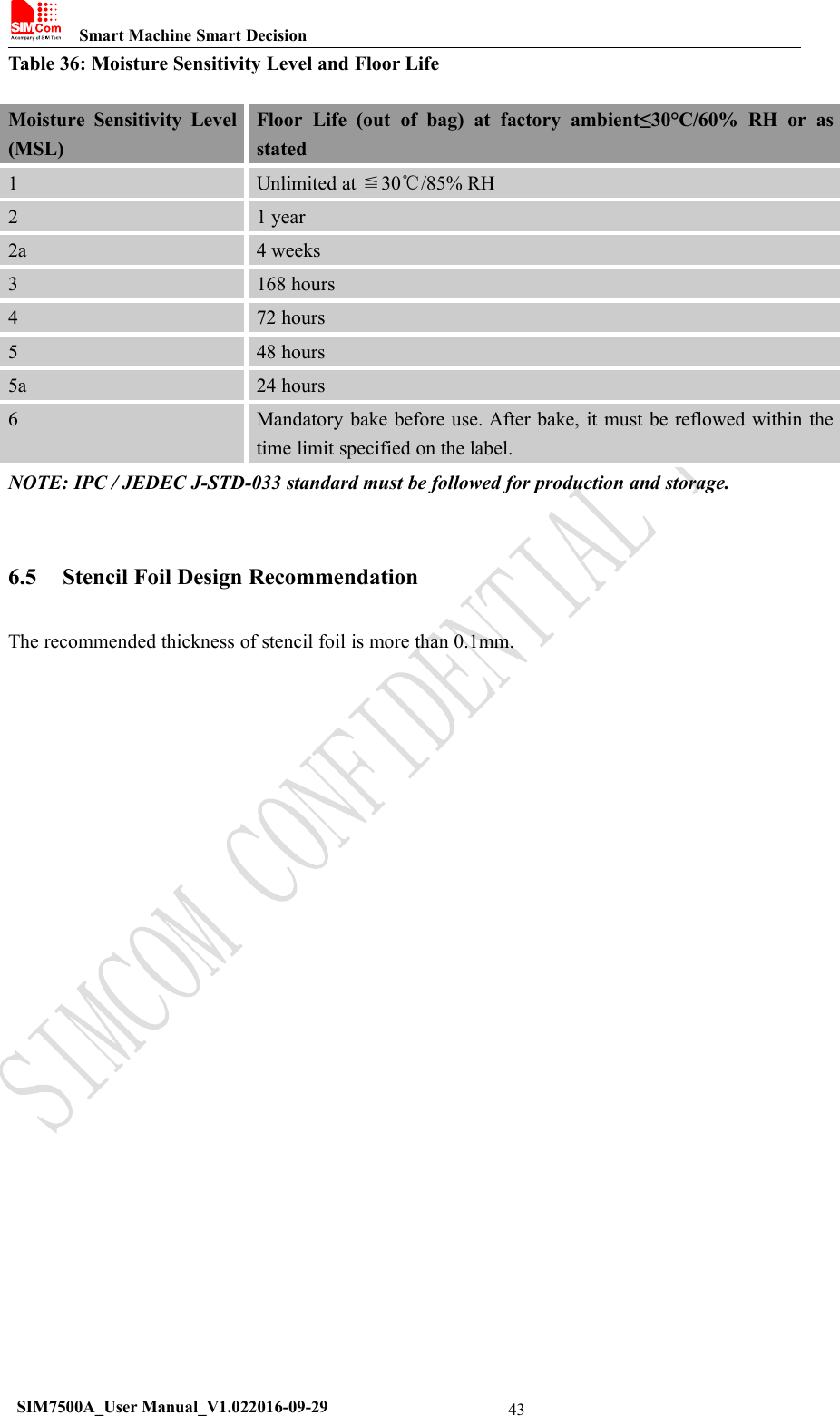
Smart Machine Smart DecisionSIM7500A_User Manual_V1.022016-09-2942Table 35: The Description of Label InformationNo.DescriptionALOGOBNo.1 PinCProject NameDPart NumberESerial Number (SN)FInternational Mobile Equipment Identity (IMEI)GFCC IDHQR code6.3 Typical SMT Reflow ProfileSIMCom provides a typical soldering profile. Therefore the soldering profile shown below is onlya generic recommendation and should be adjusted to the specific application and manufacturingconstraints.Figure 33: The ramp-soak-spike Reflow Profile of ModuleNote: For more details about secondary SMT, please refer to the document [21].6.4 Moisture Sensitivity Level (MSL)Module is qualified to Moisture Sensitivity Level (MSL) 3 in accordance with JEDEC J-STD-033.If the prescribed time limit is exceeded, users should bake modules for 192 hours in dryingequipment (<5% RH) at 40+5/-0°C, or 72 hours at 85+5/-5°C. Note that plastic tray is notheat-resistant, and only can be baked at 45° C.
Smart Machine Smart DecisionSIM7500A_User Manual_V1.022016-09-2943Table 36: Moisture Sensitivity Level and Floor LifeMoisture Sensitivity Level(MSL)Floor Life (out of bag) at factory ambient≤30°C/60% RH or asstated1Unlimited at ≦30℃/85% RH21 year2a4 weeks3168 hours472 hours548 hours5a24 hours6Mandatory bake before use. After bake, it must be reflowed within thetime limit specified on the label.NOTE: IPC / JEDEC J-STD-033 standard must be followed for production and storage.6.5 Stencil Foil Design RecommendationThe recommended thickness of stencil foil is more than 0.1mm.
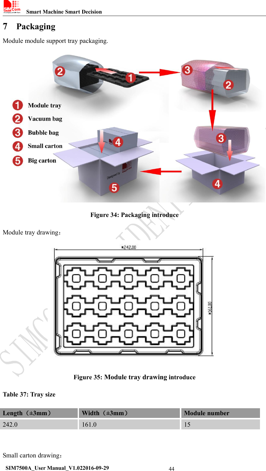
Smart Machine Smart DecisionSIM7500A_User Manual_V1.022016-09-29447PackagingModule module support tray packaging.Figure 34: Packaging introduceModule tray drawing:Figure 35: Module tray drawing introduceTable 37: Tray sizeLength(±3mm)Width(±3mm)Module number242.0161.015Small carton drawing:
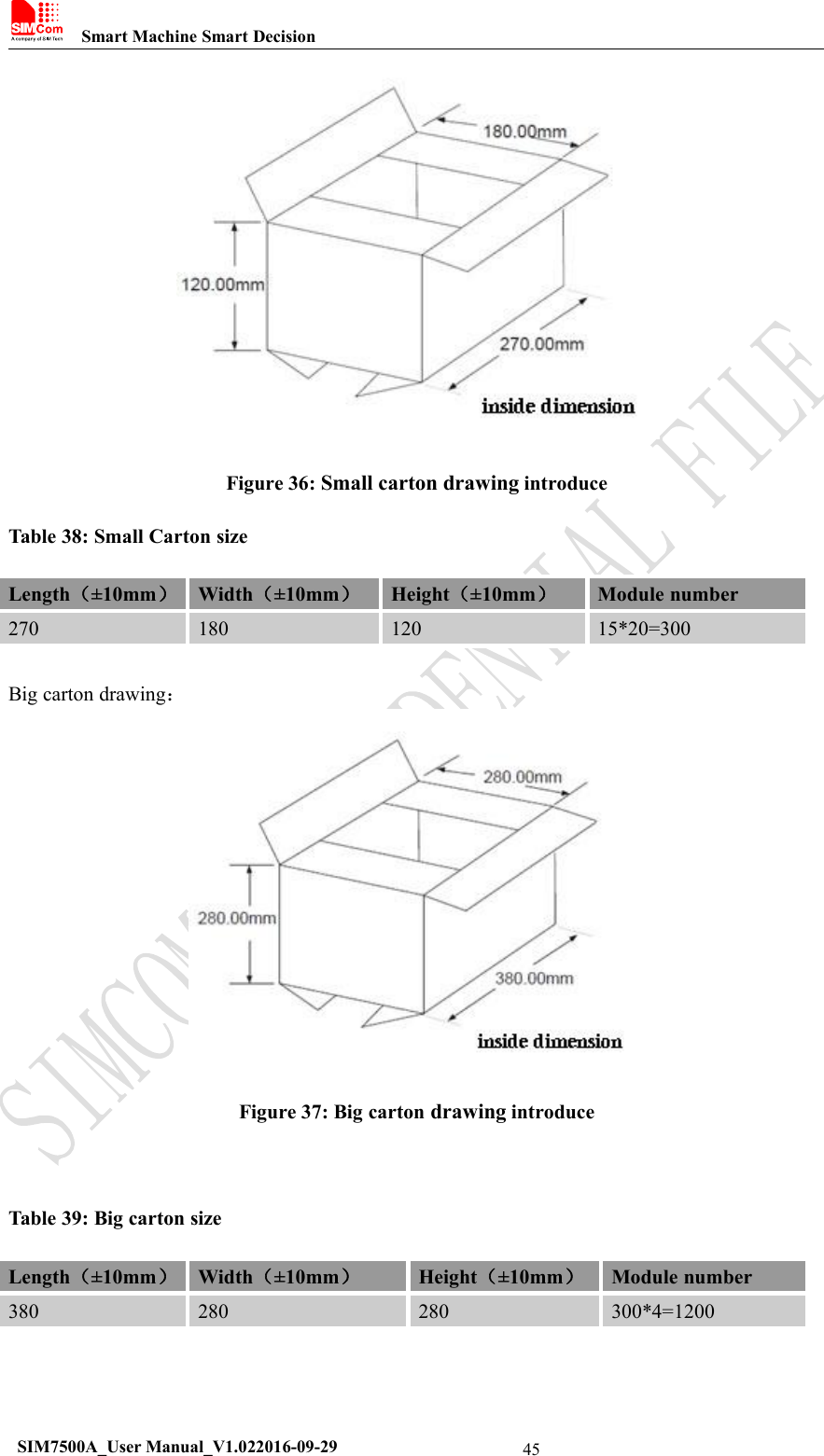
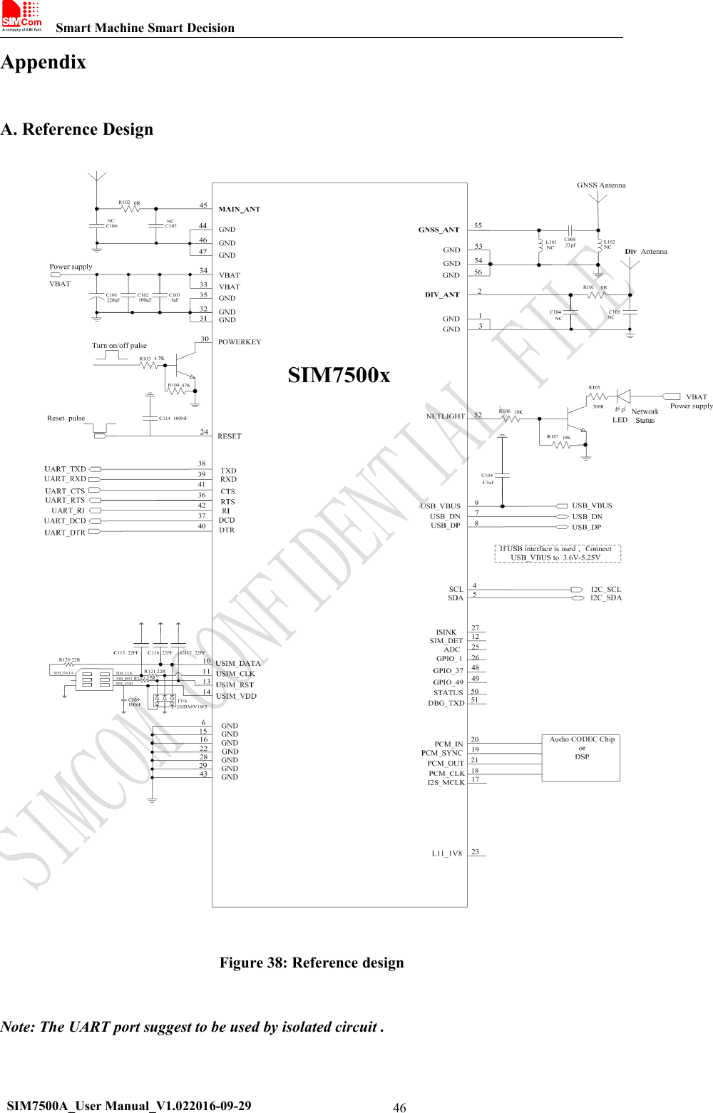
Smart Machine Smart DecisionSIM7500A_User Manual_V1.022016-09-2945Figure 36: Small carton drawing introduceTable 38: Small Carton sizeLength(±10mm)Width(±10mm)Height(±10mm)Module number27018012015*20=300Big carton drawing:Figure 37: Big carton drawing introduceTable 39: Big carton sizeLength(±10mm)Width(±10mm)Height(±10mm)Module number380280280300*4=1200
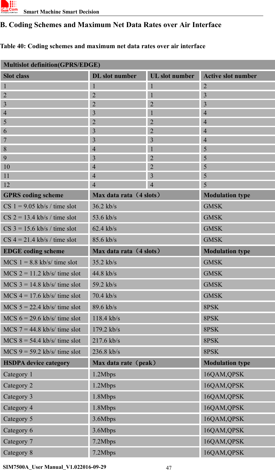
Smart Machine Smart DecisionSIM7500A_User Manual_V1.022016-09-2946AppendixA. Reference DesignFigure 38: Reference designNote: The UART port suggest to be used by isolated circuit .
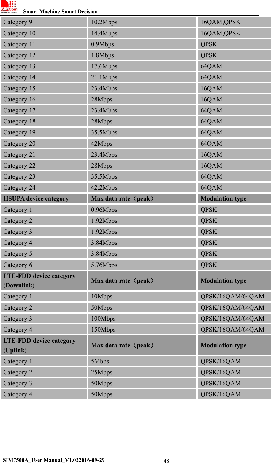
Smart Machine Smart DecisionSIM7500A_User Manual_V1.022016-09-2947B. Coding Schemes and Maximum Net Data Rates over Air InterfaceTable 40: Coding schemes and maximum net data rates over air interfaceMultislot definition(GPRS/EDGE)Slot classDL slot numberUL slot numberActive slot number111222133223431452246324733484159325104251143512445GPRS coding schemeMax data rata(4 slots)Modulation typeCS 1 = 9.05 kb/s / time slot36.2 kb/sGMSKCS 2 = 13.4 kb/s / time slot53.6 kb/sGMSKCS 3 = 15.6 kb/s / time slot62.4 kb/sGMSKCS 4 = 21.4 kb/s / time slot85.6 kb/sGMSKEDGE coding schemeMax data rata(4 slots)Modulation typeMCS 1 = 8.8 kb/s/ time slot35.2 kb/sGMSKMCS 2 = 11.2 kb/s/ time slot44.8 kb/sGMSKMCS 3 = 14.8 kb/s/ time slot59.2 kb/sGMSKMCS 4 = 17.6 kb/s/ time slot70.4 kb/sGMSKMCS 5 = 22.4 kb/s/ time slot89.6 kb/s8PSKMCS 6 = 29.6 kb/s/ time slot118.4 kb/s8PSKMCS 7 = 44.8 kb/s/ time slot179.2 kb/s8PSKMCS 8 = 54.4 kb/s/ time slot217.6 kb/s8PSKMCS 9 = 59.2 kb/s/ time slot236.8 kb/s8PSKHSDPA device categoryMax data rate(peak)Modulation typeCategory 11.2Mbps16QAM,QPSKCategory 21.2Mbps16QAM,QPSKCategory 31.8Mbps16QAM,QPSKCategory 41.8Mbps16QAM,QPSKCategory 53.6Mbps16QAM,QPSKCategory 63.6Mbps16QAM,QPSKCategory 77.2Mbps16QAM,QPSKCategory 87.2Mbps16QAM,QPSK
Smart Machine Smart DecisionSIM7500A_User Manual_V1.022016-09-2948Category 910.2Mbps16QAM,QPSKCategory 1014.4Mbps16QAM,QPSKCategory 110.9MbpsQPSKCategory 121.8MbpsQPSKCategory 1317.6Mbps64QAMCategory 1421.1Mbps64QAMCategory 1523.4Mbps16QAMCategory 1628Mbps16QAMCategory 1723.4Mbps64QAMCategory 1828Mbps64QAMCategory 1935.5Mbps64QAMCategory 2042Mbps64QAMCategory 2123.4Mbps16QAMCategory 2228Mbps16QAMCategory 2335.5Mbps64QAMCategory 2442.2Mbps64QAMHSUPA device categoryMax data rate(peak)Modulation typeCategory 10.96MbpsQPSKCategory 21.92MbpsQPSKCategory 31.92MbpsQPSKCategory 43.84MbpsQPSKCategory 53.84MbpsQPSKCategory 65.76MbpsQPSKLTE-FDD device category(Downlink)Max data rate(peak)Modulation typeCategory 110MbpsQPSK/16QAM/64QAMCategory 250MbpsQPSK/16QAM/64QAMCategory 3100MbpsQPSK/16QAM/64QAMCategory 4150MbpsQPSK/16QAM/64QAMLTE-FDD device category(Uplink)Max data rate(peak)Modulation typeCategory 15MbpsQPSK/16QAMCategory 225MbpsQPSK/16QAMCategory 350MbpsQPSK/16QAMCategory 450MbpsQPSK/16QAM
Smart Machine Smart DecisionSIM7500A_User Manual_V1.022016-09-2949C. Related DocumentsTable 41: Related documentsSNTitleDescription[1]SIM7X00 Series_ATCommand Manual_V1.xxSIM7X00 Series_AT Command Manual[2]ITU-T Draft newrecommendationV.25terSerial asynchronous automatic dialing and control[3]GSM 07.07Digital cellular telecommunications (Phase 2+); AT commandset for GSM Mobile Equipment (ME)[4]GSM 07.10Support GSM 07.10 multiplexing protocol[5]GSM 07.05Digital cellular telecommunications (Phase 2+); Use of DataTerminal Equipment – Data Circuit terminating Equipment(DTE – DCE) interface for Short Message Service (SMS)and Cell Broadcast Service (CBS)[6]GSM 11.14Digital cellular telecommunications system (Phase 2+);Specification of the SIM Application Toolkit for theSubscriber Identity Module – Mobile Equipment (SIM – ME)interface[7]GSM 11.11Digital cellular telecommunications system (Phase 2+);Specification of the Subscriber Identity Module – MobileEquipment (SIM – ME) interface[8]GSM 03.38Digital cellular telecommunications system (Phase 2+);Alphabets and language-specific information[9]GSM 11.10Digital cellular telecommunications system (Phase 2) ;Mobile Station (MS) conformance specification ;Part 1:Conformance specification[10]3GPP TS 51.010-1Digital cellular telecommunications system (Release 5);Mobile Station (MS) conformance specification[11]3GPP TS 34.124Electromagnetic Compatibility (EMC) for mobile terminalsand ancillary equipment.[12]3GPP TS 34.121Electromagnetic Compatibility (EMC) for mobile terminalsand ancillary equipment.[13]3GPP TS 34.123-1Technical Specification Group Radio Access Network;Terminal conformance specification; Radio transmission andreception (FDD)[14]3GPP TS 34.123-3User Equipment (UE) conformance specification; Part 3:Abstract Test Suites.[15]EN 301 908-02 V2.2.1Electromagnetic compatibility and Radio spectrum Matters(ERM); Base Stations (BS) and User Equipment (UE) forIMT-2000. Third Generation cellular networks; Part 2:Harmonized EN for IMT-2000, CDMA Direct Spread(UTRA FDD) (UE) covering essential requirements of article3.2 of the R&TTE Directive[16]EN 301 489-24 V1.2.1Electromagnetic compatibility and Radio Spectrum Matters(ERM); Electromagnetic Compatibility (EMC) standard forradio equipment and services; Part 24: Specific conditions forIMT-2000 CDMA Direct Spread (UTRA) for Mobile andportable (UE) radio and ancillary equipment[17]IEC/EN60950-1(2001)Safety of information technology equipment (2000)[18]3GPP TS 51.010-1Digital cellular telecommunications system (Release 5);Mobile Station (MS) conformance specification
Smart Machine Smart DecisionSIM7500A_User Manual_V1.022016-09-2950[19]GCF-CC V3.23.1Global Certification Forum - Certification Criteria[20]2002/95/ECDirective of the European Parliament and of the Council of27 January 2003 on the restriction of the use of certainhazardous substances in electrical and electronic equipment(RoHS)[21]Modulesecondary-SMT-UGD-V1.xxModule secondary SMT Guidelines[22]SIM7X00Series_UART_ApplicationNote_V1.xxSIM7X00 Series_UART_Application Note[23]SIM7X00 Series_USBAUDIO_ApplicationNote_V1.xxSIM7X00 Series_USB AUDIO_Application Note[24]Antenna design guidelines fordiversity receiver systemAntenna design guidelines for diversity receiver system[25]SIM7X00 Series_Sleep Mode_Application Note_V1.xxSIM7X00 Series_Sleep Mode_ Application Note
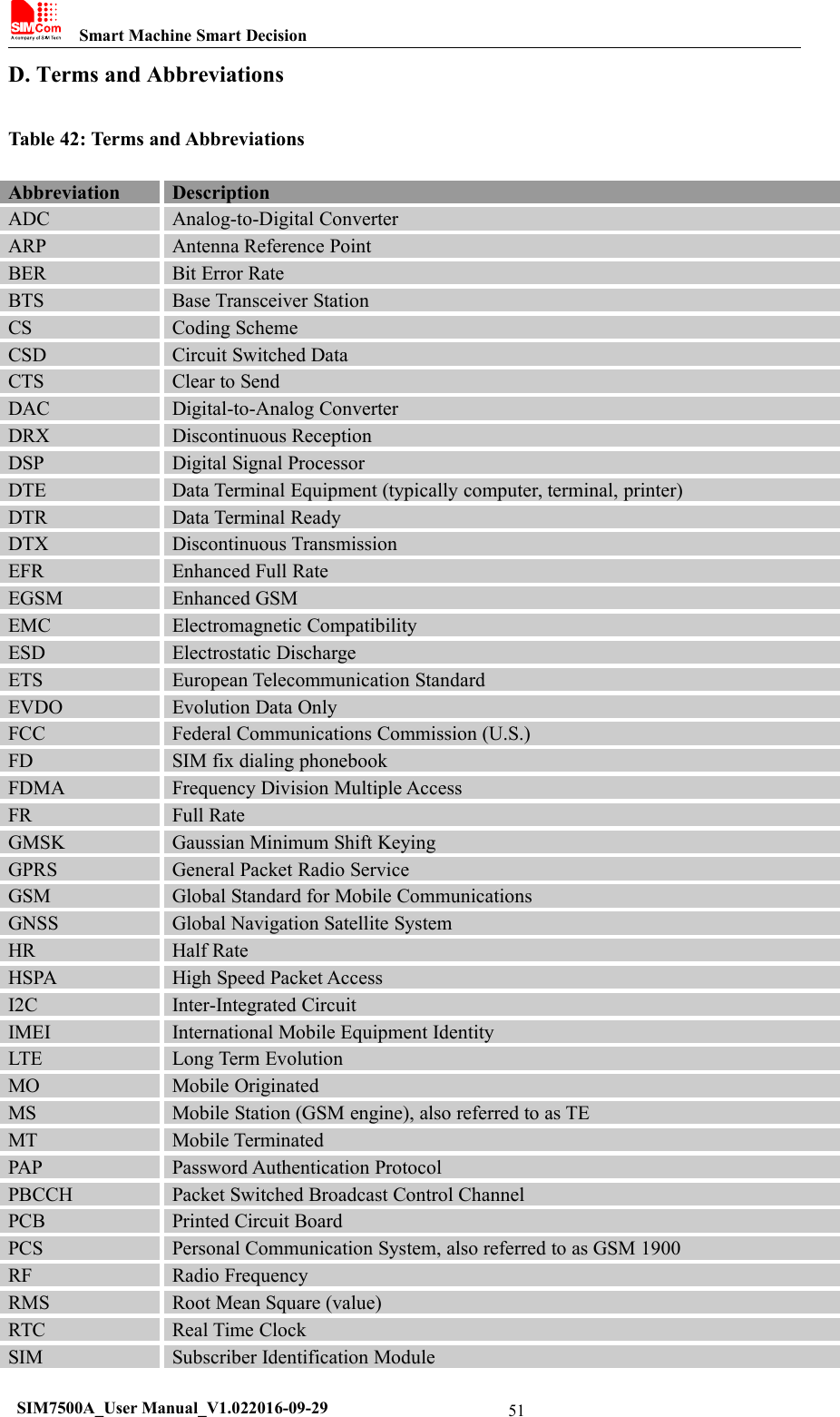
Smart Machine Smart DecisionSIM7500A_User Manual_V1.022016-09-2951D. Terms and AbbreviationsTable 42: Terms and AbbreviationsAbbreviationDescriptionADCAnalog-to-Digital ConverterARPAntenna Reference PointBERBit Error RateBTSBase Transceiver StationCSCoding SchemeCSDCircuit Switched DataCTSClear to SendDACDigital-to-Analog ConverterDRXDiscontinuous ReceptionDSPDigital Signal ProcessorDTEData Terminal Equipment (typically computer, terminal, printer)DTRData Terminal ReadyDTXDiscontinuous TransmissionEFREnhanced Full RateEGSMEnhanced GSMEMCElectromagnetic CompatibilityESDElectrostatic DischargeETSEuropean Telecommunication StandardEVDOEvolution Data OnlyFCCFederal Communications Commission (U.S.)FDSIM fix dialing phonebookFDMAFrequency Division Multiple AccessFRFull RateGMSKGaussian Minimum Shift KeyingGPRSGeneral Packet Radio ServiceGSMGlobal Standard for Mobile CommunicationsGNSSGlobal Navigation Satellite SystemHRHalf RateHSPAHigh Speed Packet AccessI2CInter-Integrated CircuitIMEIInternational Mobile Equipment IdentityLTELong Term EvolutionMOMobile OriginatedMSMobile Station (GSM engine), also referred to as TEMTMobile TerminatedPAPPassword Authentication ProtocolPBCCHPacket Switched Broadcast Control ChannelPCBPrinted Circuit BoardPCSPersonal Communication System, also referred to as GSM 1900RFRadio FrequencyRMSRoot Mean Square (value)RTCReal Time ClockSIMSubscriber Identification Module
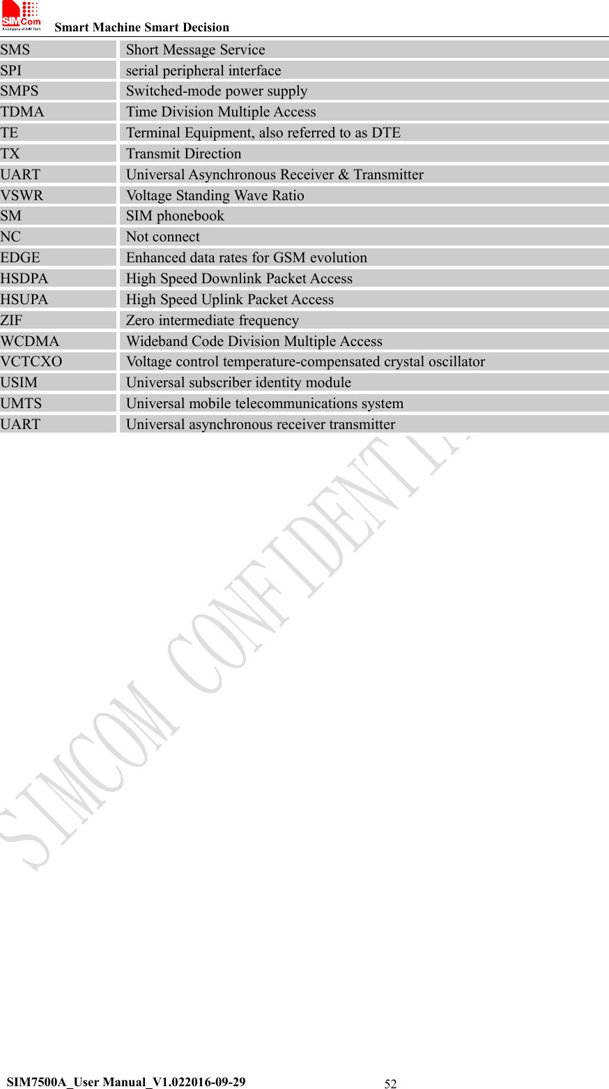
Smart Machine Smart DecisionSIM7500A_User Manual_V1.022016-09-2952SMSShort Message ServiceSPIserial peripheral interfaceSMPSSwitched-mode power supplyTDMATime Division Multiple AccessTETerminal Equipment, also referred to as DTETXTransmit DirectionUARTUniversal Asynchronous Receiver & TransmitterVSWRVoltage Standing Wave RatioSMSIM phonebookNCNot connectEDGEEnhanced data rates for GSM evolutionHSDPAHigh Speed Downlink Packet AccessHSUPAHigh Speed Uplink Packet AccessZIFZero intermediate frequencyWCDMAWideband Code Division Multiple AccessVCTCXOVoltage control temperature-compensated crystal oscillatorUSIMUniversal subscriber identity moduleUMTSUniversal mobile telecommunications systemUARTUniversal asynchronous receiver transmitter
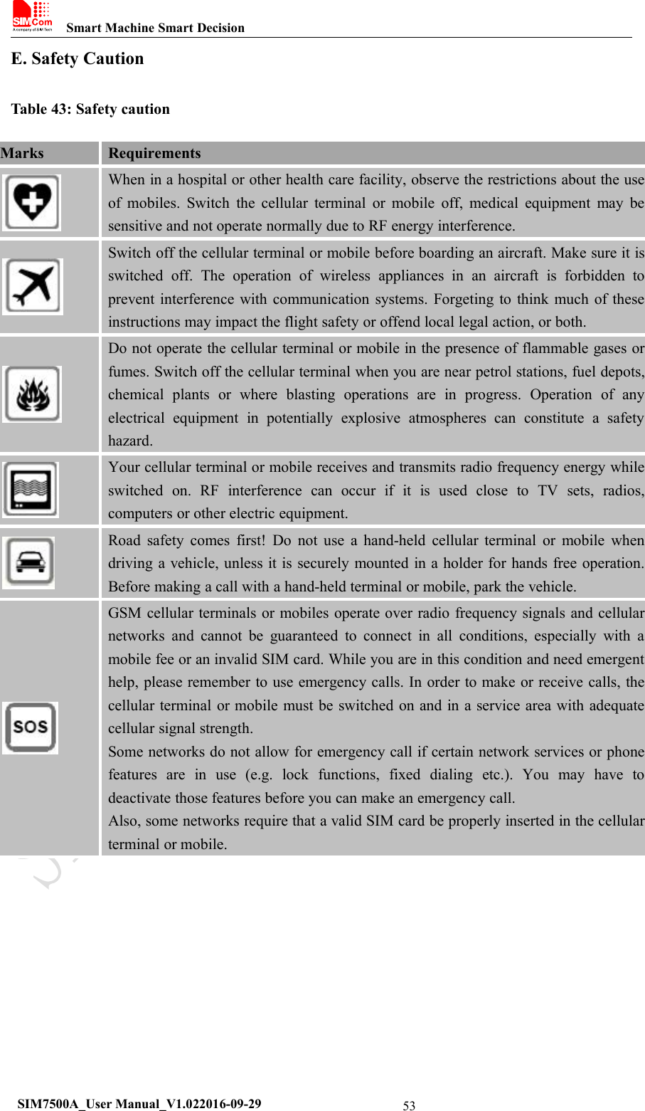
Smart Machine Smart DecisionSIM7500A_User Manual_V1.022016-09-2953E. Safety CautionTable 43: Safety cautionMarksRequirementsWhen in a hospital or other health care facility, observe the restrictions about the useof mobiles. Switch the cellular terminal or mobile off, medical equipment may besensitive and not operate normally due to RF energy interference.Switch off the cellular terminal or mobile before boarding an aircraft. Make sure it isswitched off. The operation of wireless appliances in an aircraft is forbidden toprevent interference with communication systems. Forgeting to think much of theseinstructions may impact the flight safety or offend local legal action, or both.Do not operate the cellular terminal or mobile in the presence of flammable gases orfumes. Switch off the cellular terminal when you are near petrol stations, fuel depots,chemical plants or where blasting operations are in progress. Operation of anyelectrical equipment in potentially explosive atmospheres can constitute a safetyhazard.Your cellular terminal or mobile receives and transmits radio frequency energy whileswitched on. RF interference can occur if it is used close to TV sets, radios,computers or other electric equipment.Road safety comes first! Do not use a hand-held cellular terminal or mobile whendriving a vehicle, unless it is securely mounted in a holder for hands free operation.Before making a call with a hand-held terminal or mobile, park the vehicle.GSM cellular terminals or mobiles operate over radio frequency signals and cellularnetworks and cannot be guaranteed to connect in all conditions, especially with amobile fee or an invalid SIM card. While you are in this condition and need emergenthelp, please remember to use emergency calls. In order to make or receive calls, thecellular terminal or mobile must be switched on and in a service area with adequatecellular signal strength.Some networks do not allow for emergency call if certain network services or phonefeatures are in use (e.g. lock functions, fixed dialing etc.). You may have todeactivate those features before you can make an emergency call.Also, some networks require that a valid SIM card be properly inserted in the cellularterminal or mobile.
Smart Machine Smart DecisionSIM7500A_User Manual_V1.022016-09-2954Contact us:Shanghai SIMCom Wireless Solutions Ltd.Add: SIM Technology Building, No.633, Jinzhong Road, Changning District, Shanghai P.R. China200335Tel:+86 21 3235 3300Fax:+86 21 3235 3020URL:www.simcomm2m.com

Navigation menu