Silicon Laboratories Finland WF111 IEEE 802.11 b/g/n Wi-Fi module WF111 User Manual Product Data Sheet
Silicon Laboratories Finland Oy IEEE 802.11 b/g/n Wi-Fi module WF111 Product Data Sheet
Contents
- 1. User Manual and Installations
- 2. User Manual
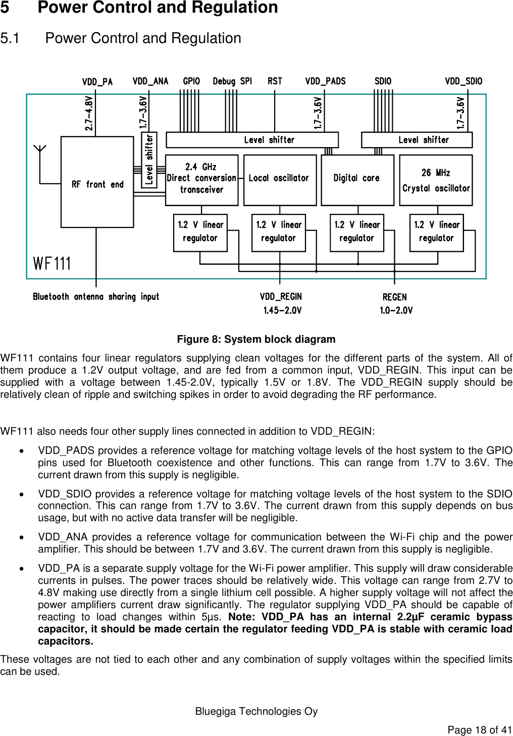
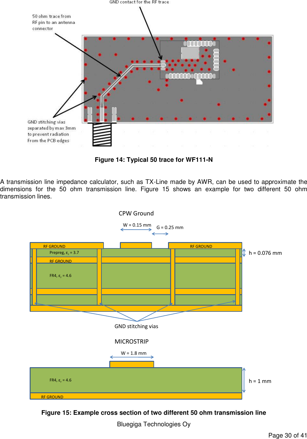
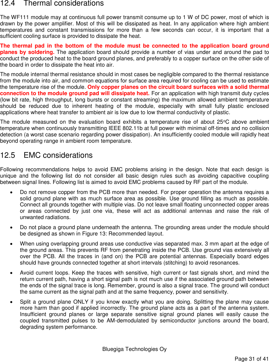
User Manual
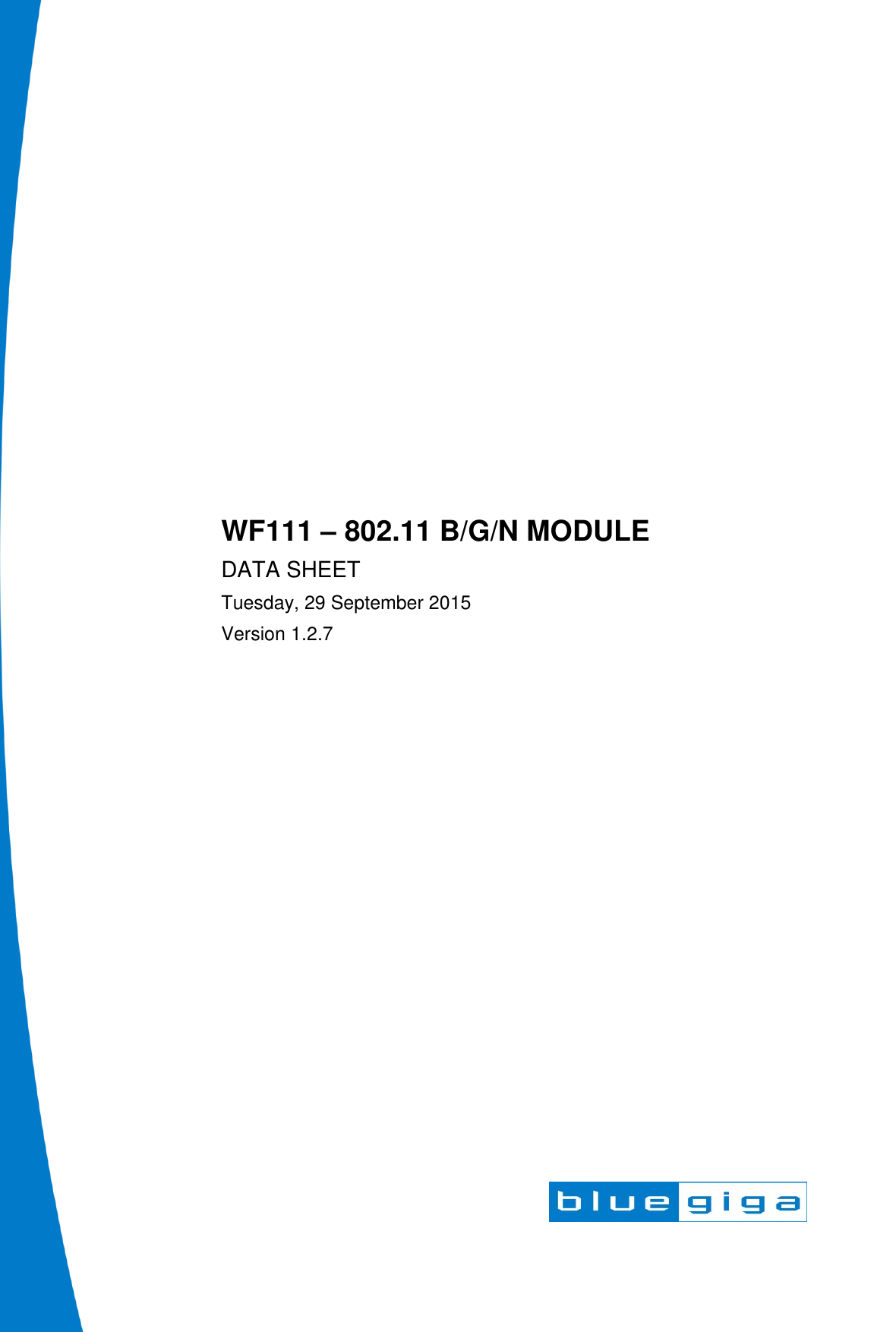
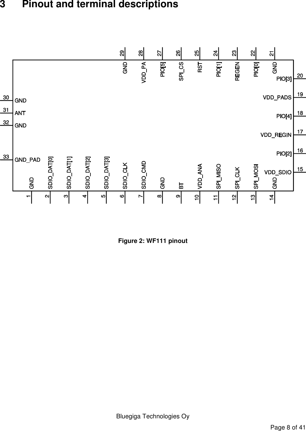
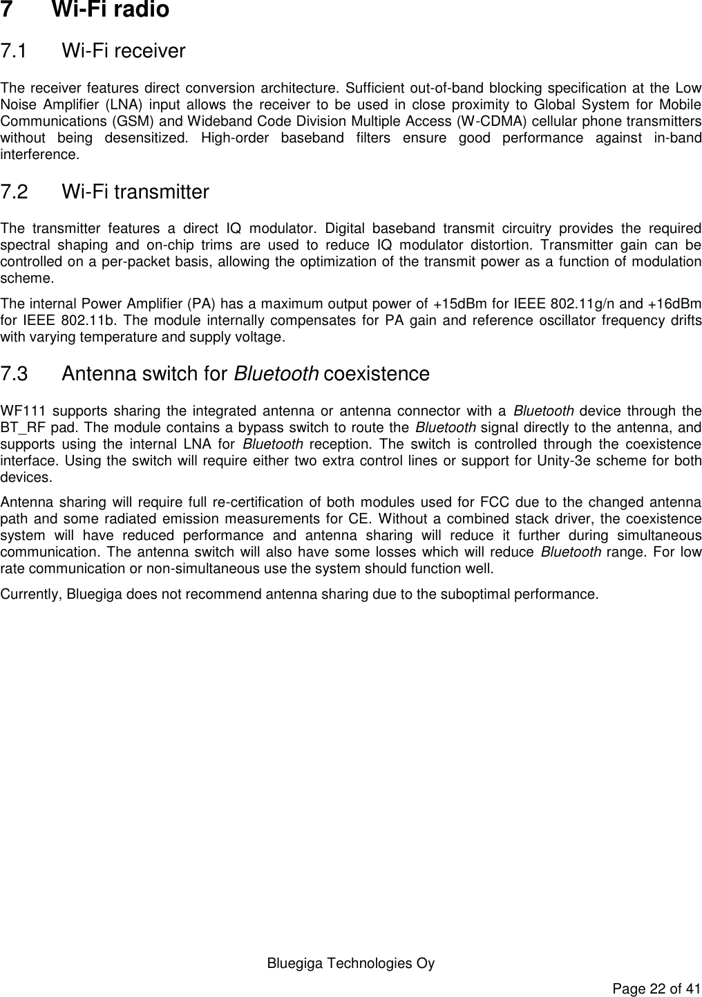
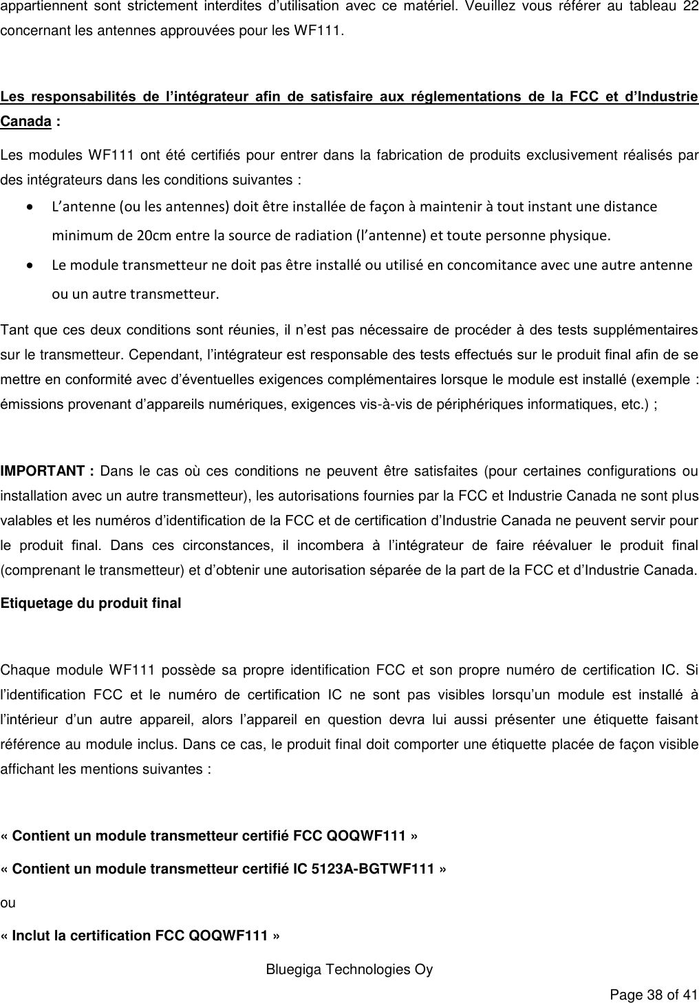
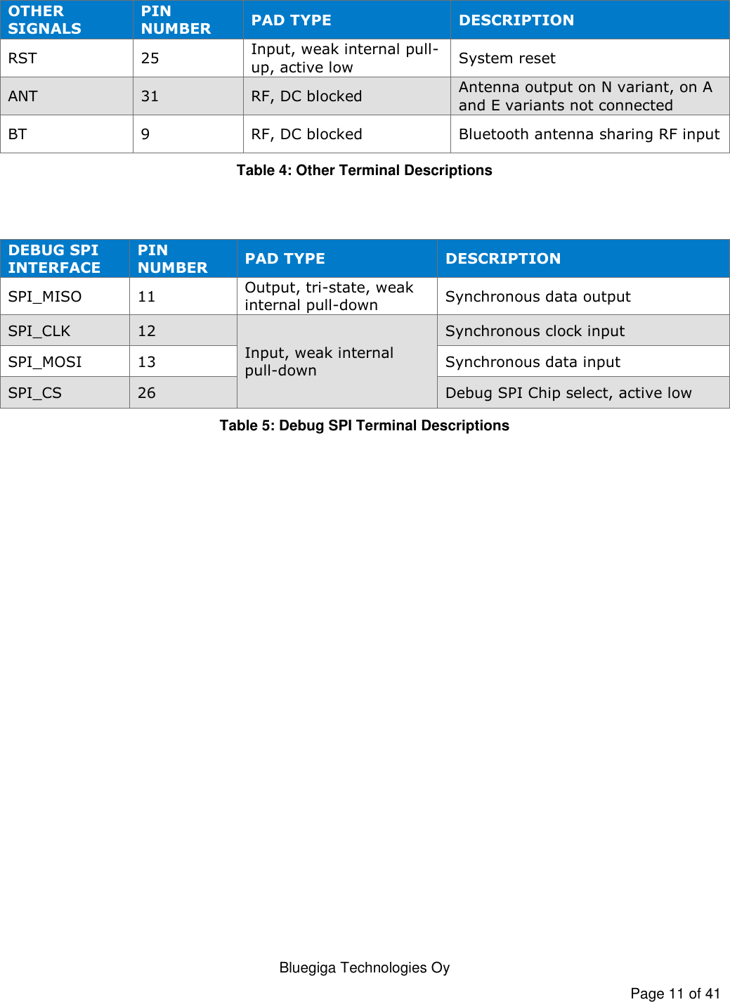
![Bluegiga Technologies Oy Page 9 of 41 POWER SUPPLIES PIN NUMBER DESCRIPTION VDD_REGIN 17 Input for the internal regulators REGEN 23 Pull high to enable internal voltage regulators (2.0V max) GND 1, 8, 14, 21, 29, 30, 32 Ground GND_PAD 33 Thermal pad, on bottom of WF111 VDD_ANA 10 Positive supply for PA control VDD_PADS 19 Positive supply for the digital interfaces VDD_SDIO 15 Positive supply for the SDIO interface VDD_PA 28 Positive supply for the power amplifier Table 1: Supply Terminal Descriptions PIO PORT PIN NUMBER PAD TYPE DESCRIPTION PIO[0] 22 Bi-directional, programmable strength internal pull-down/pull-up Programmable input/output line. Can be used for Bluetooth co-existence. PIO[1] 24 PIO[2] 16 PIO[3] 20 PIO[4] 18 PIO[5] 27 Table 2: GPIO Terminal Descriptions](https://usermanual.wiki/Silicon-Laboratories-Finland/WF111.User-Manual/User-Guide-2770627-Page-9.png)
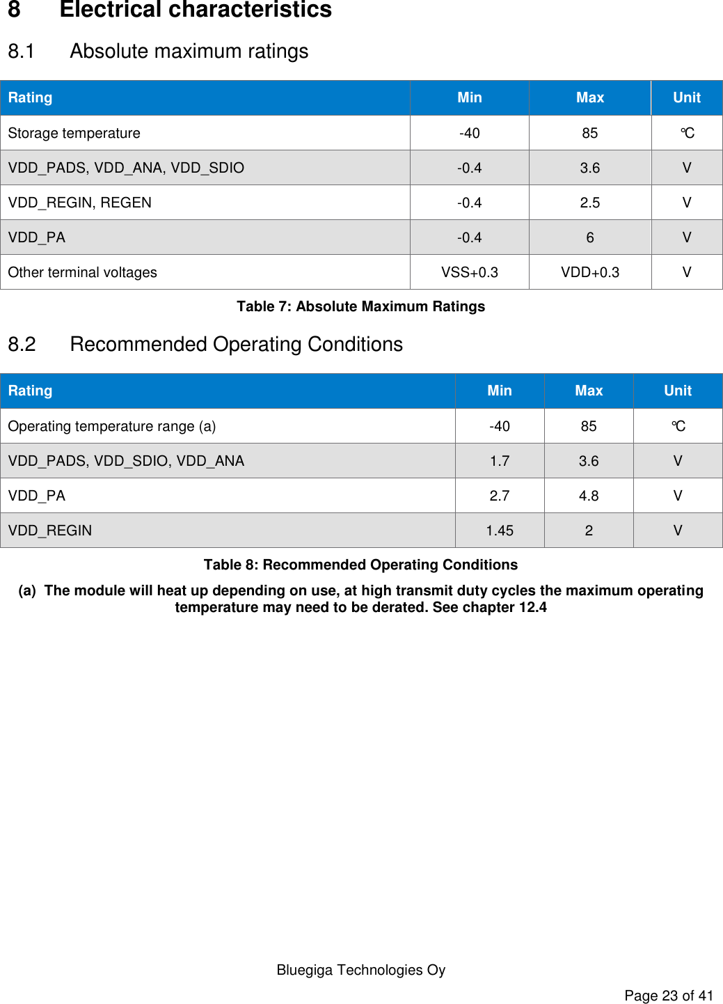
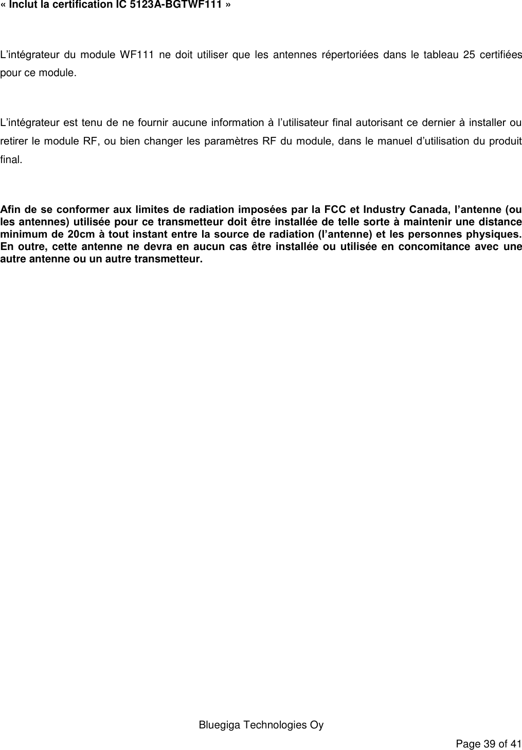
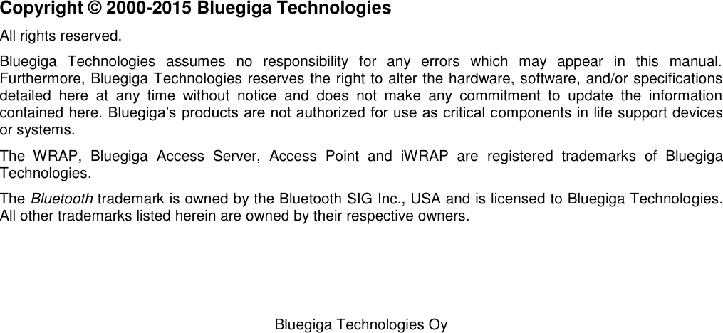
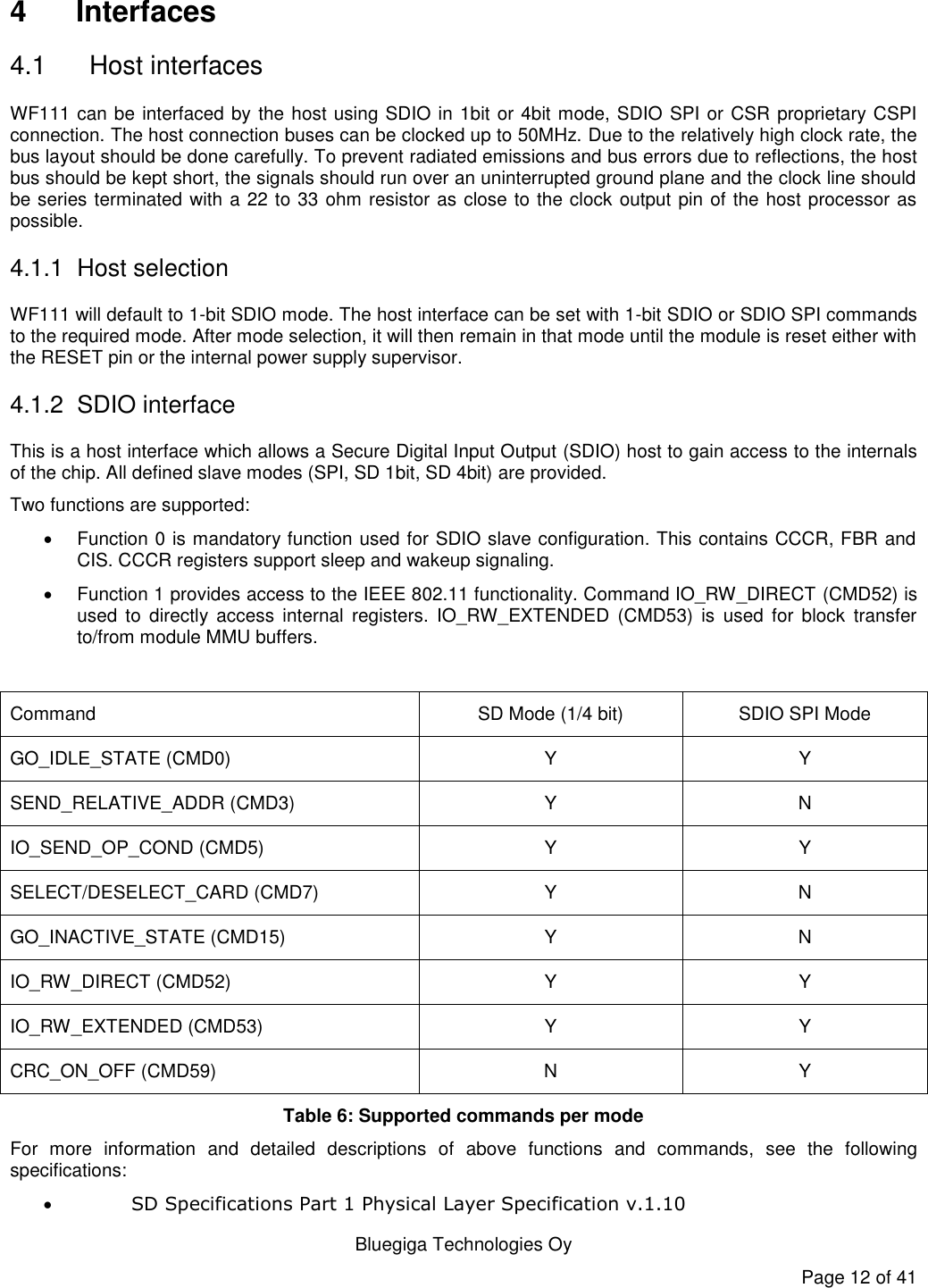
![Bluegiga Technologies Oy Page 10 of 41 SDIO/CSPI Interfaces PIN NUMBER PAD TYPE DESCRIPTION SDIO_DATA[0] 2 Bi-directional, tri-state, weak internal pull-up Synchronous data input/output SDIO_SPI_DI SDIO SPI data output CSPI_MISO CSPI data output SDIO_DATA[1] 3 Synchronous data input/output SDIO_SPI_INT SDIO SPI interrupt output CSPI_INT CSPI data input SDIO_DATA[2] 4 Synchronous data input/output SDIO_DATA[3] 5 Bi-directional, weak/strong internal pull-up Synchronous data input/output SDIO_SPI_CS# SDIO SPI chip select, active low CSPI_CS# CSPI chip select, active low SDIO_CLK 6 Input, weak internal pull-up SDIO clock SDIO_SPI_SCLK SDIO SPI clock CSPI_CLK CSPI clock SDIO_CMD 7 Bi-directional, weak internal pull-up SDIO data input SDIO_SPI_MOSI SDIO SPI data input CSPI_MOSI CSPI data input Table 3: Host Interface Terminal Descriptions](https://usermanual.wiki/Silicon-Laboratories-Finland/WF111.User-Manual/User-Guide-2770627-Page-10.png)
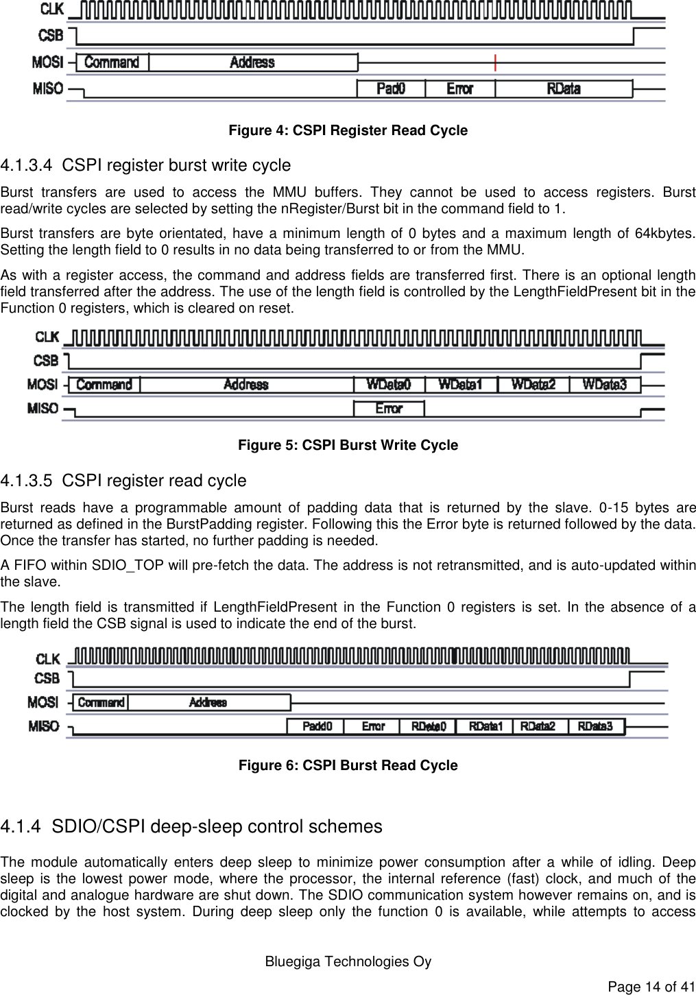
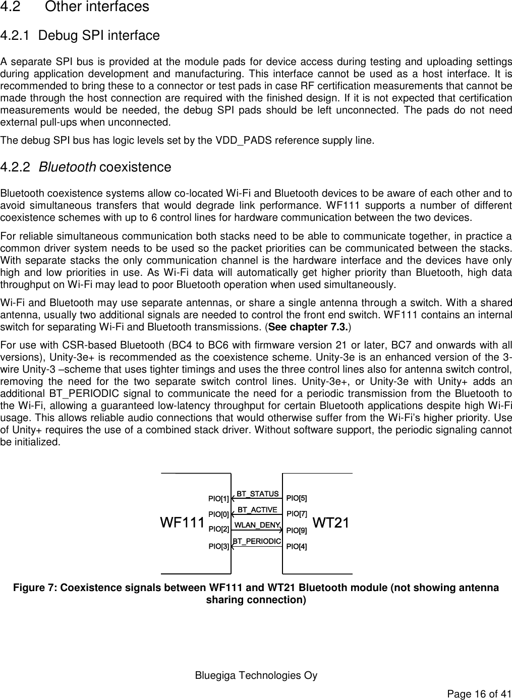
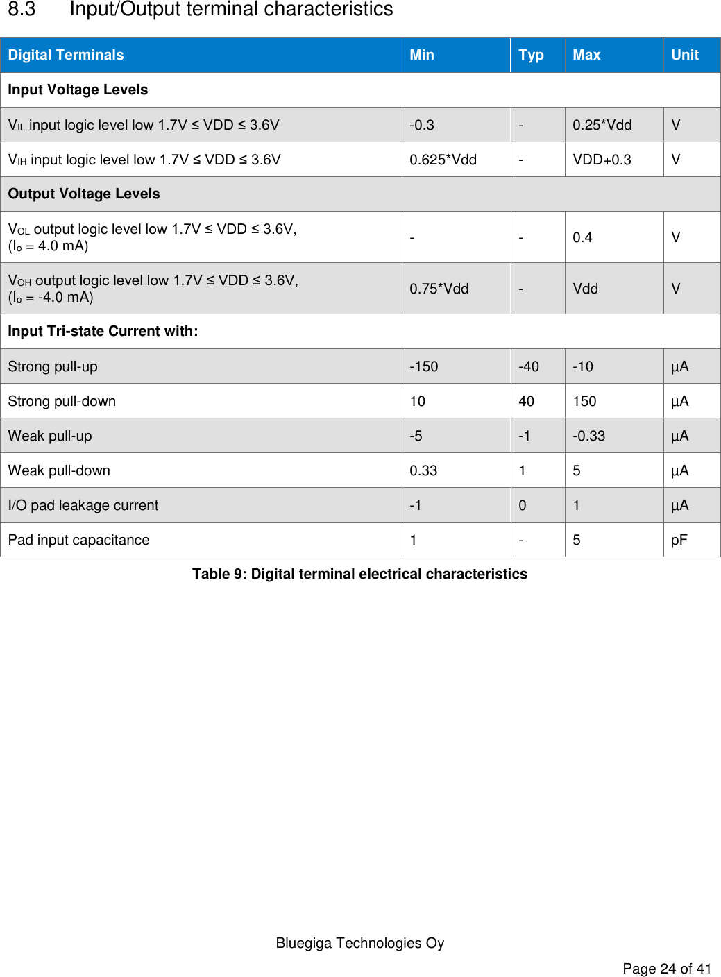
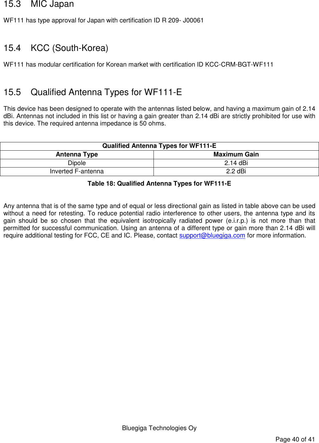
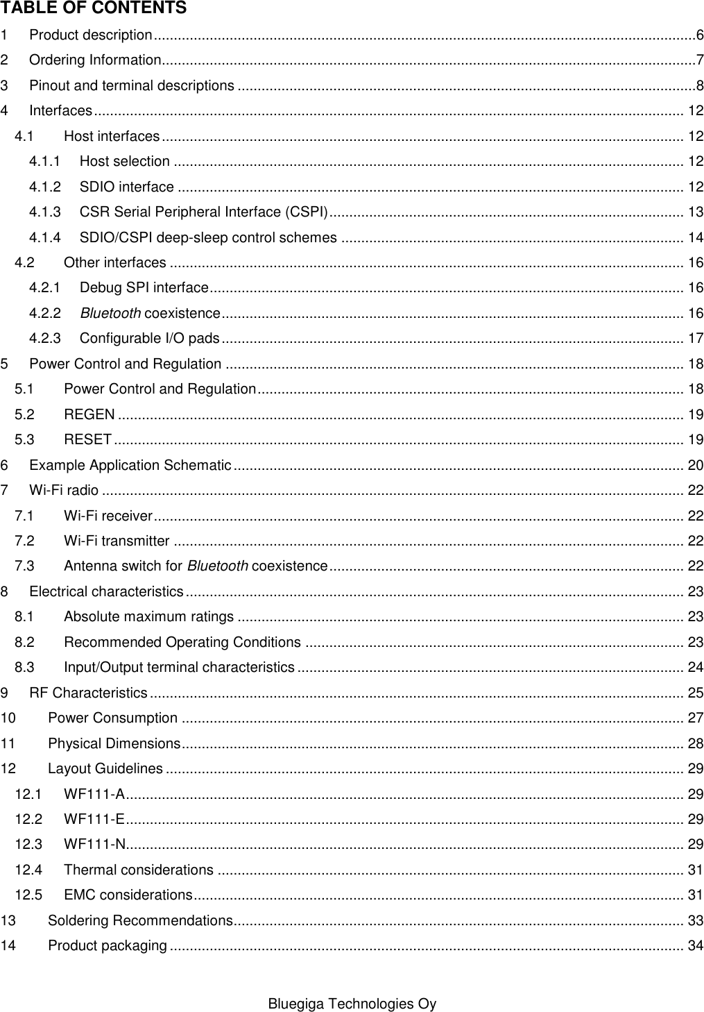
![Bluegiga Technologies Oy Page 17 of 41 Using the Unity-3e+ scheme and the pictured PIO pad bindings, the MIB file mib111_drv_coex.dat should be used. If needed, the PIO pads PIO[3], PIO[5], PIO[4] and PIO[2] can also be used for BT_STATUS, BT_ACTIVE, WLAN_DENY and BT_PERIODIC, respectively, in which case the MIB file mib111_drv_coex_alt.dat should be chosen. On the DKWF111 evaluation board, the PIO[5] pad is connected to an activity led, which is supported by the MIB files mib111_drv_led.dat and mib111_drv_coex_led.dat, the latter of which contains signal bindings for the scheme pictured above. The PSKEYs for the Unity-3e+ on the WT21 are: PSKEY_LC_COMBO_DISABLE_PIO_MASK (0x0028) = 0x0200 0x0000 0x0000 PSKEY_LC_COMBO_DOT11_CHANNEL_PIO_BASE (0x002A) = 0x0011 PSKEY_LC_COMBO_DOT11_ESCO_RTX_PRIORITY ( 0x0050) = 0x0001 PSKEY_LC_COMBO_DOT11_PULL_DISABLE_MASK (0x005A) = 0x0200 PSKEY_LC_COMBO_DOT11_PERIODIC_PIO_MASK (0x005C) = 0x0010 0x0000 PSKEY_LC_COMBO_DOT11_T1 (0x005E) = 0x0043 PSKEY_LC_COMBO_DOT11_T2 (0x005F) = 0x000A PSKEY_TXRX_PIO_CONTROL (0x0209) = 0x0001 WF111 has hardware support for 3-wire, 4-wire, Unity-3e and Unity+ coexistence schemes. The default MIB files support only Unity-3e with Unity+. For other coexistence schemes a custom MIB is required, for more information please contact Bluegiga technical support. 4.2.3 Configurable I/O pads A number of programmable bi-directional input/outputs (I/O) are provided. PIO[0:5] logic levels are referred to the VDD_PADS supply line. PIO lines can be configured through software to implement various automated functions or as generic inputs or outputs. As inputs the lines can be configured to have either weak or strong pull-ups or pull-downs. All PIO lines are configured as inputs with weak pull-downs at reset. In addition to the coexistence functions, any of the PIO lines can be configured as interrupt request lines, wake-up lines from sleep modes, status led drivers with multiple internally generated modes, general I/O pins controlled by the host, or as a 32.768 kHz sleep clock input. For further information, please contact Bluegiga technical support. Note: All unused signals can be left floating. The GPIO lines have internal pull-downs.](https://usermanual.wiki/Silicon-Laboratories-Finland/WF111.User-Manual/User-Guide-2770627-Page-17.png)