SIMCom Wireless Solutions SIM7000A LTE CAT-M1(eMTC) and NB-IoT Module User Manual SIM7000A V1 00

Shanghai SIMCom Wireless Solutions Limited LTE CAT-M1(eMTC) and NB-IoT Module SIM7000A V1 00

Contents

SIM7000A__User Manual_V1 00
SIM7000A_User Manual_V1.01
Smart Machine Smart DecisionSIM7000 _Hardware Design _V1.00 2017-05-23Document TitleSIM7000A_User ManualVersion1.00Date2017-5-23StatusReleasedDocument Control IDSIM7000A_User Manual_V1.01Compliance InformationFCC Compliance Statement: This device complies the FCC Rules . Operation is subject to thefollowing two conditions: 1. This device may not cause harmful interference, and 2. This devicemust accept any interference received, including interference that may cause undesired operation.This device must accept any interference received, including interference that may cause undesiredoperation. Product that is a radio transmitter is labeled with FCC ID.FCC Caution:(1)Exposure to Radio Frequency Radiation. This equipment must be installed and operated inaccordance with provided instructions and the antenna(s) used for this transmitter must be installedto provide a separation distance of at least 20 cm from all persons and must not be collocated oroperating in conjunction with any other antenna or transmitter. End-users and installers must beprovided with antenna installation instructions and transmitter operating conditions for satisfyingRF exposure compliance.(2) Any changes or modifications not expressly approved by the grantee of this device could voidthe user's authority to operate the equipment.(3) This Transmitter must not be co-located or operating in conjunction with any other antenna ortransmitter.(4) Changes or modifications to this unit not expressly approved by the party responsible forcompliance could void the user authority to operate the equipment.(5) the modules FCC ID is not visible when installed in the host, or(6) if the host is marketed so that end users do not have straight forward commonly used methodsfor access to remove the module so that the FCC ID of the module is visible; then an additionalpermanent label referring to the enclosed module: Contains Transmitter Module FCC ID:2AJYU-SIM7000A or Contains FCC ID: 2AJYU-SIM7000A must be used.
Smart Machine Smart DecisionSIM7000 _Hardware Design _V1.00 2017-05-23General NotesSIMCom offers this information as a service to its customers to support the application andengineering efforts that use the products designed by SIMCom. The information provided is basedon the requirements specifically from the customers. SIMCom has not undertaken any independentsearch for additional relevant information, including any information that may be in the customer’spossession. Furthermore, the system validation of the product designed by SIMCom within a largerelectronic system remains the responsibility of the customer or the customer’s system integrator.All specifications supplied herein are subject to change without notice.CopyrightThis document contains the proprietary technical information which is the property of SIMComLimited, copying of this document, giving it to others, the using or communication of the contentsthereof are forbidden without the official authority by SIMCom. Offenders are liable to thepayment of the damages. All rights are reserved in the event of grant of a patent or the registrationof a utility model or design. All specifications supplied herein are subject to change without noticeCopyright © SIMCom Wireless Solutions Co., Ltd. 2017
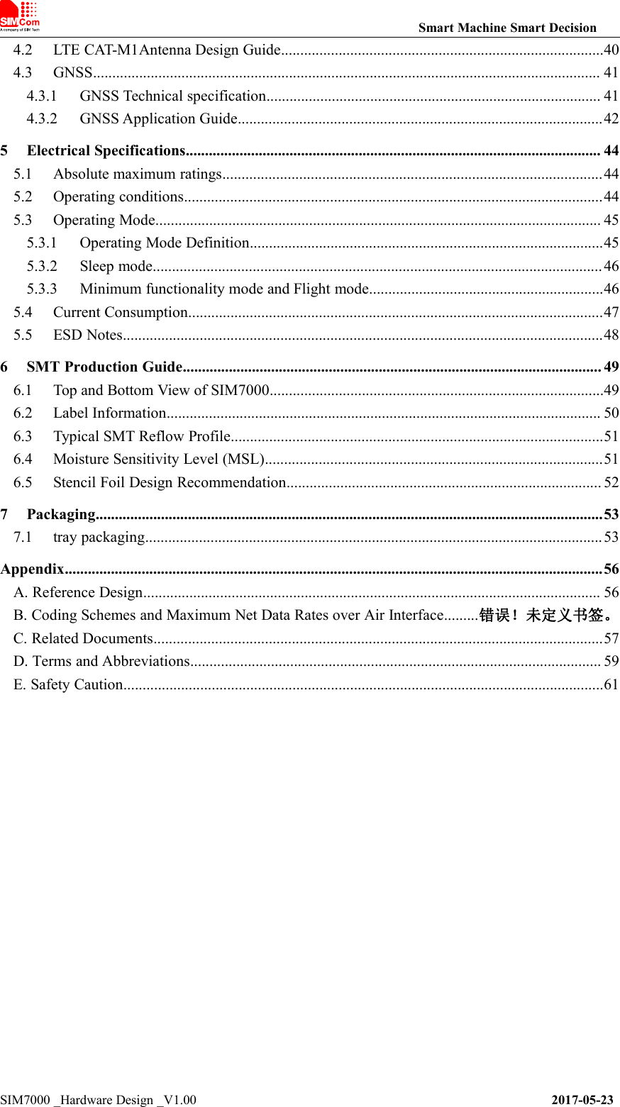
Smart Machine Smart DecisionSIM7000 _Hardware Design _V1.00 2017-05-23ContentsContents............................................................................................................................................... 4Table Index.......................................................................................................................................... 6Figure Index........................................................................................................................................ 7Revision History..................................................................................................................................81 Introduction..................................................................................................................................91.1 Product Outline....................................................................................................................... 91.2 Hardware Interface Overview...............................................................................................101.3 Hardware Block Diagram..................................................................................................... 111.4 Functional Overview.............................................................................................................122 Package Information................................................................................................................. 142.1 Pin Assignment Overview.................................................................................................... 142.2 Pin Description......................................................................................................................162.3 Mechanical Information........................................................................................................192.4 Footprint Recommendation.................................................................................................. 203 Interface Application.................................................................................................................213.1 Power Supply........................................................................................................................ 213.1.1 Power Supply Design Guide..........................................................................................223.1.2 Recommended Power Supply Circuit............................................................................223.1.3 Voltage Monitor............................................................................................................. 233.2 Power on/Power off/Reset Function.....................................................................................243.2.1 Power on........................................................................................................................ 243.2.2 Power off........................................................................................................................253.2.3 Reset Function................................................................................................................263.3 UART Interface.....................................................................................................................273.3.1 UART Design Guide......................................................................................................273.3.2 RI and DTR Behavior.................................................................................................... 283.4 USB Interface........................................................................................................................293.5 SIM Interface........................................................................................................................ 303.5.1 SIM Application Guide..................................................................................................303.5.2 Recommended SIM Card Holder.................................................................................. 313.6 PCM Interface.......................................................................................................................323.6.1 PCM timing....................................................................................................................323.6.2 PCM Application Guide.................................................................................................343.7 I2C Interface......................................................................................................................... 343.8 Network status...................................................................................................................... 343.9 Other interface...................................................................................................................... 353.9.1 ADC............................................................................................................................... 353.9.2 LDO................................................................................................................................364 RF Specifications........................................................................................................................374.1 LTE CAT-M1RF Specifications............................................................................................37
Smart Machine Smart DecisionSIM7000 _Hardware Design _V1.00 2017-05-234.2 LTE CAT-M1Antenna Design Guide....................................................................................404.3 GNSS.................................................................................................................................... 414.3.1 GNSS Technical specification....................................................................................... 414.3.2 GNSS Application Guide...............................................................................................425 Electrical Specifications............................................................................................................ 445.1 Absolute maximum ratings...................................................................................................445.2 Operating conditions.............................................................................................................445.3 Operating Mode.................................................................................................................... 455.3.1 Operating Mode Definition............................................................................................455.3.2 Sleep mode.....................................................................................................................465.3.3 Minimum functionality mode and Flight mode.............................................................465.4 Current Consumption............................................................................................................475.5 ESD Notes.............................................................................................................................486 SMT Production Guide............................................................................................................. 496.1 Top and Bottom View of SIM7000.......................................................................................496.2 Label Information................................................................................................................. 506.3 Typical SMT Reflow Profile.................................................................................................516.4 Moisture Sensitivity Level (MSL)........................................................................................516.5 Stencil Foil Design Recommendation.................................................................................. 527 Packaging....................................................................................................................................537.1 tray packaging.......................................................................................................................53Appendix............................................................................................................................................56A. Reference Design....................................................................................................................... 56B. Coding Schemes and Maximum Net Data Rates over Air Interface.........错误!未定义书签。C. Related Documents.....................................................................................................................57D. Terms and Abbreviations........................................................................................................... 59E. Safety Caution.............................................................................................................................61
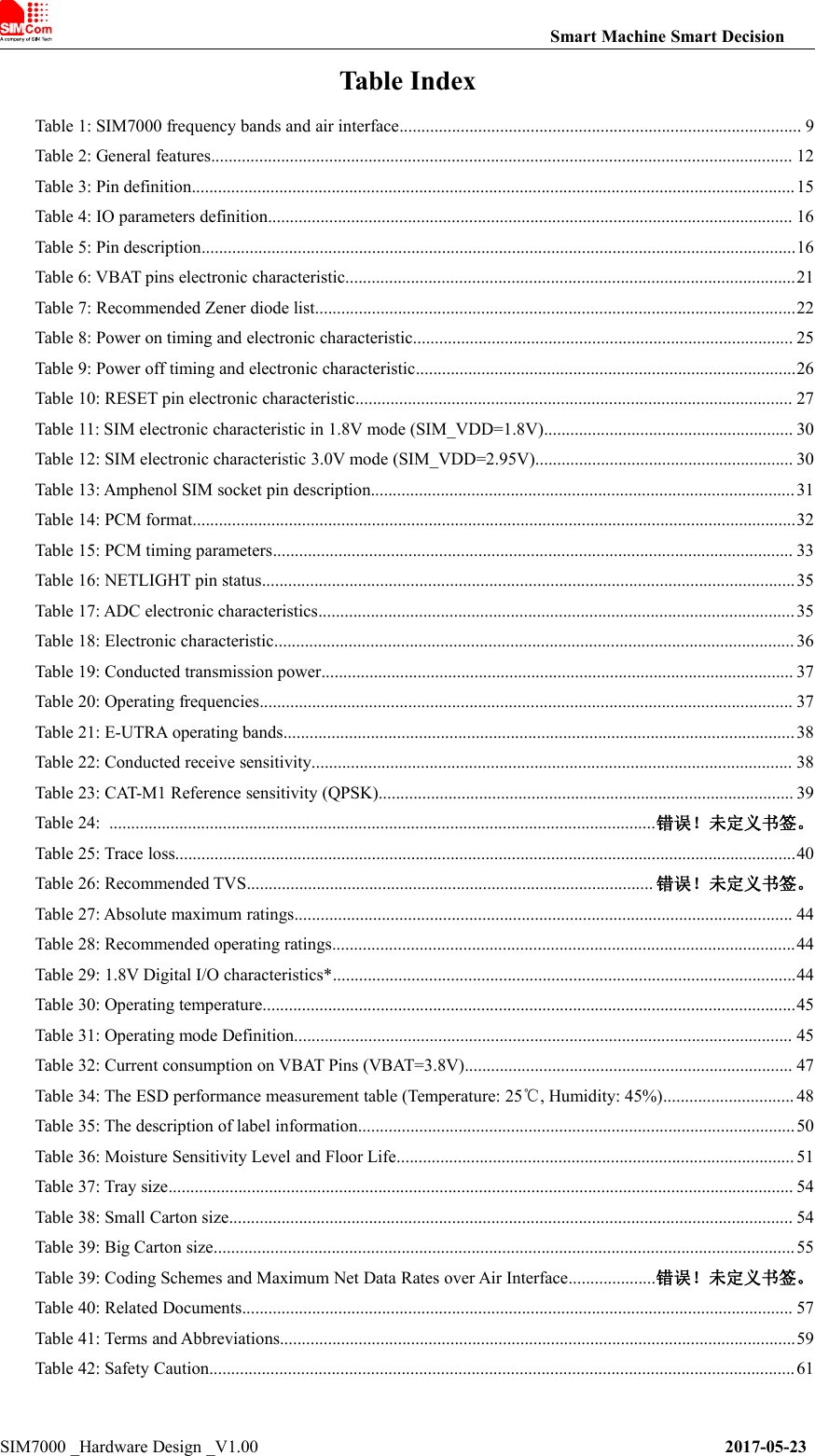
Smart Machine Smart DecisionSIM7000 _Hardware Design _V1.00 2017-05-23Table IndexTable 1: SIM7000 frequency bands and air interface............................................................................................ 9Table 2: General features..................................................................................................................................... 12Table 3: Pin definition..........................................................................................................................................15Table 4: IO parameters definition........................................................................................................................ 16Table 5: Pin description........................................................................................................................................16Table 6: VBAT pins electronic characteristic.......................................................................................................21Table 7: Recommended Zener diode list..............................................................................................................22Table 8: Power on timing and electronic characteristic....................................................................................... 25Table 9: Power off timing and electronic characteristic.......................................................................................26Table 10: RESET pin electronic characteristic.................................................................................................... 27Table 11: SIM electronic characteristic in 1.8V mode (SIM_VDD=1.8V)......................................................... 30Table 12: SIM electronic characteristic 3.0V mode (SIM_VDD=2.95V)........................................................... 30Table 13: Amphenol SIM socket pin description.................................................................................................31Table 14: PCM format..........................................................................................................................................32Table 15: PCM timing parameters....................................................................................................................... 33Table 16: NETLIGHT pin status..........................................................................................................................35Table 17: ADC electronic characteristics............................................................................................................. 35Table 18: Electronic characteristic....................................................................................................................... 36Table 19: Conducted transmission power............................................................................................................ 37Table 20: Operating frequencies.......................................................................................................................... 37Table 21: E-UTRA operating bands..................................................................................................................... 38Table 22: Conducted receive sensitivity.............................................................................................................. 38Table 23: CAT-M1 Reference sensitivity (QPSK)............................................................................................... 39Table 24: .............................................................................................................................错误!未定义书签。Table 25: Trace loss..............................................................................................................................................40Table 26: Recommended TVS............................................................................................. 错误!未定义书签。Table 27: Absolute maximum ratings.................................................................................................................. 44Table 28: Recommended operating ratings..........................................................................................................44Table 29: 1.8V Digital I/O characteristics*..........................................................................................................44Table 30: Operating temperature..........................................................................................................................45Table 31: Operating mode Definition.................................................................................................................. 45Table 32: Current consumption on VBAT Pins (VBAT=3.8V)........................................................................... 47Table 34: The ESD performance measurement table (Temperature: 25℃, Humidity: 45%).............................. 48Table 35: The description of label information....................................................................................................50Table 36: Moisture Sensitivity Level and Floor Life........................................................................................... 51Table 37: Tray size............................................................................................................................................... 54Table 38: Small Carton size................................................................................................................................. 54Table 39: Big Carton size.....................................................................................................................................55Table 39: Coding Schemes and Maximum Net Data Rates over Air Interface....................错误!未定义书签。Table 40: Related Documents.............................................................................................................................. 57Table 41: Terms and Abbreviations......................................................................................................................59Table 42: Safety Caution......................................................................................................................................61
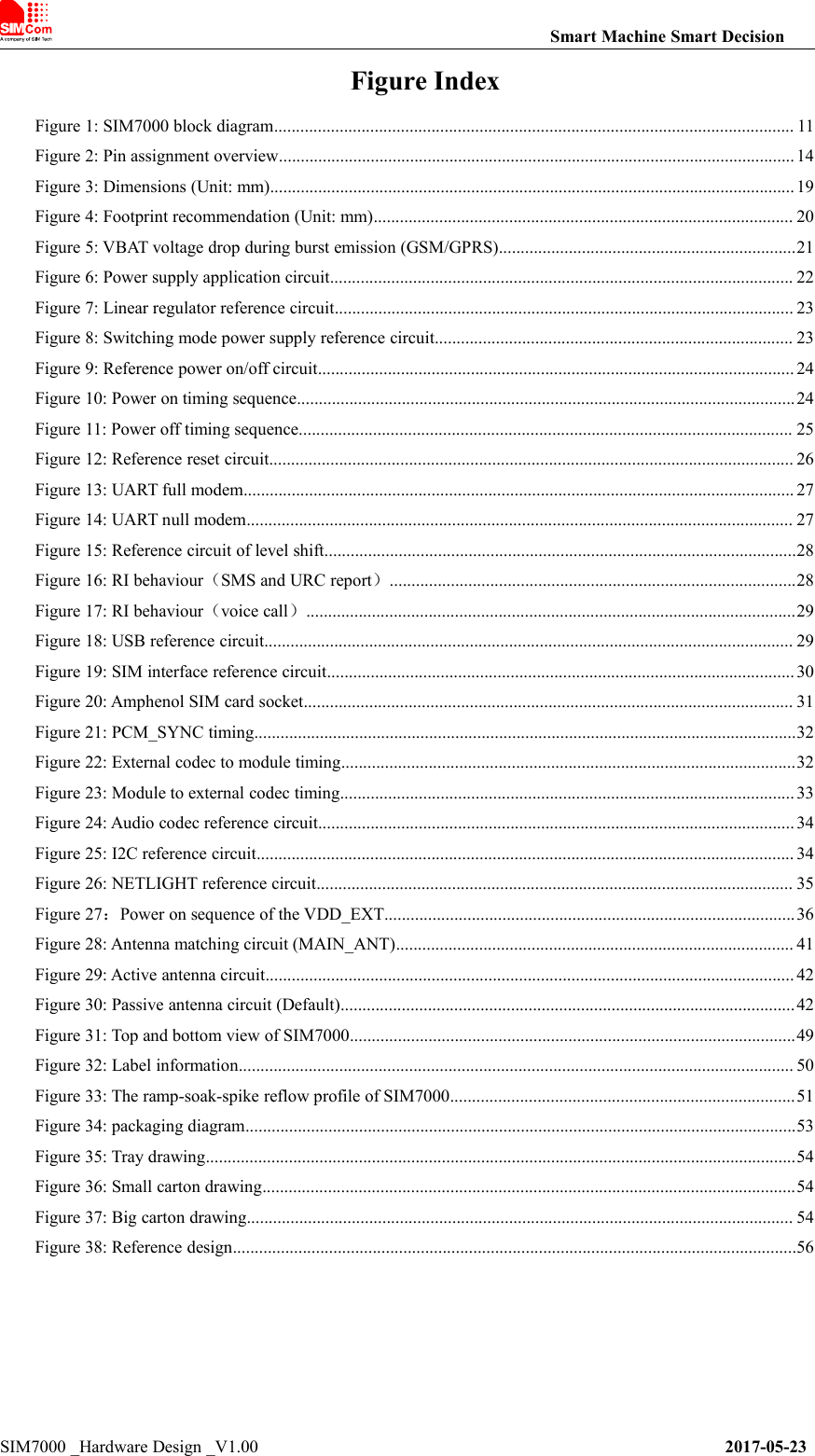
Smart Machine Smart DecisionSIM7000 _Hardware Design _V1.00 2017-05-23Figure IndexFigure 1: SIM7000 block diagram....................................................................................................................... 11Figure 2: Pin assignment overview...................................................................................................................... 14Figure 3: Dimensions (Unit: mm)........................................................................................................................ 19Figure 4: Footprint recommendation (Unit: mm)................................................................................................ 20Figure 5: VBAT voltage drop during burst emission (GSM/GPRS)....................................................................21Figure 6: Power supply application circuit.......................................................................................................... 22Figure 7: Linear regulator reference circuit......................................................................................................... 23Figure 8: Switching mode power supply reference circuit.................................................................................. 23Figure 9: Reference power on/off circuit............................................................................................................. 24Figure 10: Power on timing sequence..................................................................................................................24Figure 11: Power off timing sequence................................................................................................................. 25Figure 12: Reference reset circuit........................................................................................................................ 26Figure 13: UART full modem.............................................................................................................................. 27Figure 14: UART null modem............................................................................................................................. 27Figure 15: Reference circuit of level shift............................................................................................................28Figure 16: RI behaviour(SMS and URC report).............................................................................................28Figure 17: RI behaviour(voice call)................................................................................................................29Figure 18: USB reference circuit......................................................................................................................... 29Figure 19: SIM interface reference circuit........................................................................................................... 30Figure 20: Amphenol SIM card socket................................................................................................................ 31Figure 21: PCM_SYNC timing............................................................................................................................32Figure 22: External codec to module timing........................................................................................................32Figure 23: Module to external codec timing........................................................................................................ 33Figure 24: Audio codec reference circuit............................................................................................................. 34Figure 25: I2C reference circuit........................................................................................................................... 34Figure 26: NETLIGHT reference circuit............................................................................................................. 35Figure 27:Power on sequence of the VDD_EXT..............................................................................................36Figure 28: Antenna matching circuit (MAIN_ANT)........................................................................................... 41Figure 29: Active antenna circuit......................................................................................................................... 42Figure 30: Passive antenna circuit (Default)........................................................................................................ 42Figure 31: Top and bottom view of SIM7000......................................................................................................49Figure 32: Label information............................................................................................................................... 50Figure 33: The ramp-soak-spike reflow profile of SIM7000...............................................................................51Figure 34: packaging diagram..............................................................................................................................53Figure 35: Tray drawing.......................................................................................................................................54Figure 36: Small carton drawing..........................................................................................................................54Figure 37: Big carton drawing............................................................................................................................. 54Figure 38: Reference design.................................................................................................................................56
Smart Machine Smart DecisionSIM7000 _Hardware Design _V1.00 2017-05-23Revision HistoryDataVersionDescription of changeAuthor2017-05-231.00OriginalTu HongjunLi Ya
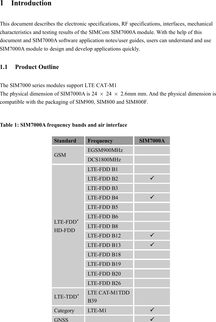
1IntroductionThis document describes the electronic specifications, RF specifications, interfaces, mechanicalcharacteristics and testing results of the SIMCom SIM7000A module. With the help of thisdocument and SIM7000A software application notes/user guides, users can understand and useSIM7000A module to design and develop applications quickly.1.1 Product OutlineThe SIM7000 series modules support LTE CAT-M1The physical dimension of SIM7000A is 24 ×24 ×2.6mm mm. And the physical dimension iscompatible with the packaging of SIM900, SIM800 and SIM800F.Table 1: SIM7000A frequency bands and air interfaceStandardFrequencySIM7000AGSMEGSM900MHzDCS1800MHzLTE-FDD*HD-FDDLTE-FDD B1LTE-FDD B2LTE-FDD B3LTE-FDD B4LTE-FDD B5LTE-FDD B6LTE-FDD B8LTE-FDD B12LTE-FDD B13LTE-FDD B18LTE-FDD B19LTE-FDD B20LTE-FDD B26LTE-TDD*LTE CAT-M1TDDB39CategoryLTE-M1GNSS
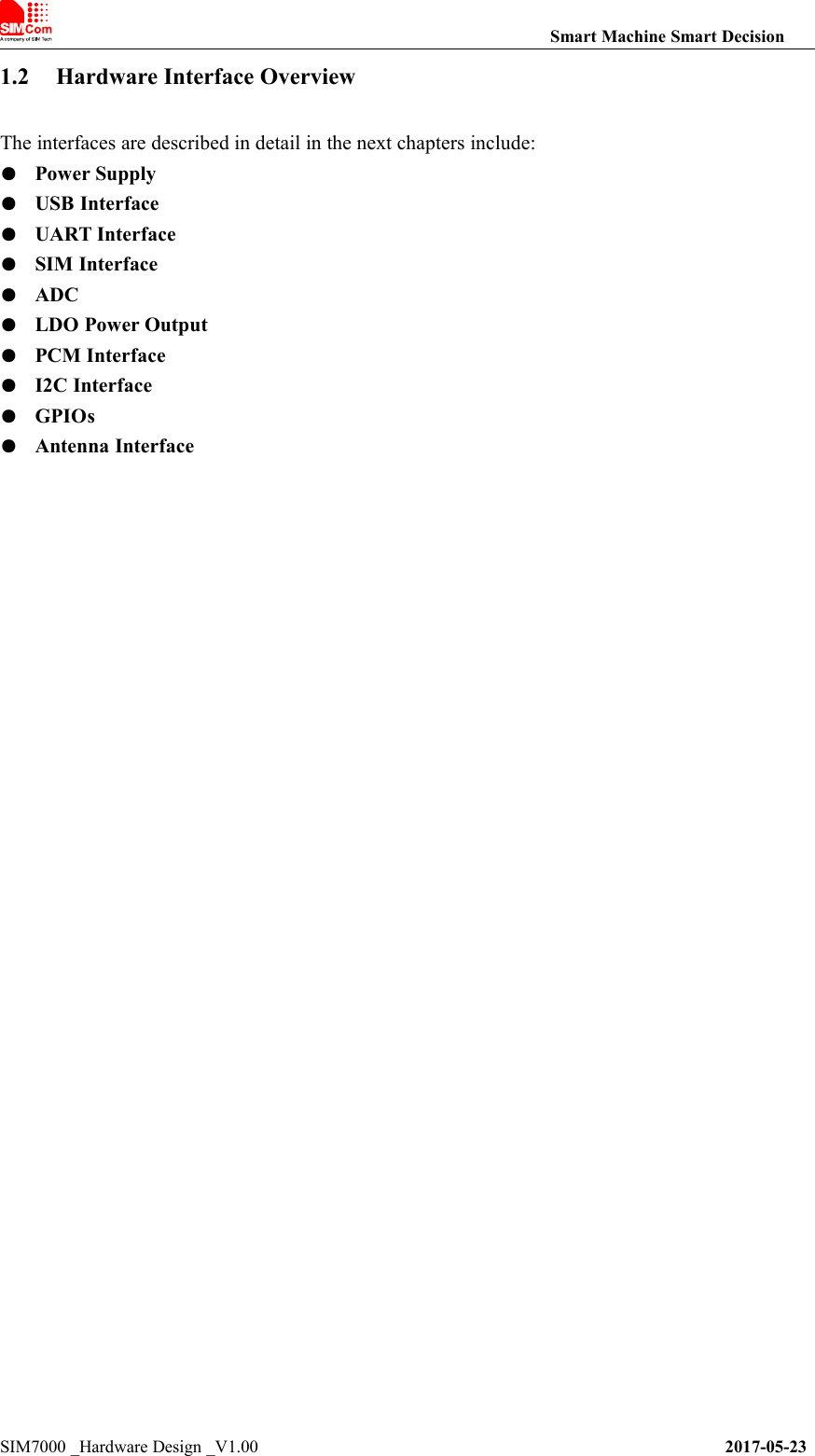
Smart Machine Smart DecisionSIM7000 _Hardware Design _V1.00 2017-05-231.2 Hardware Interface OverviewThe interfaces are described in detail in the next chapters include:●Power Supply●USB Interface●UART Interface●SIM Interface●ADC●LDO Power Output●PCM Interface●I2C Interface●GPIOs●Antenna Interface
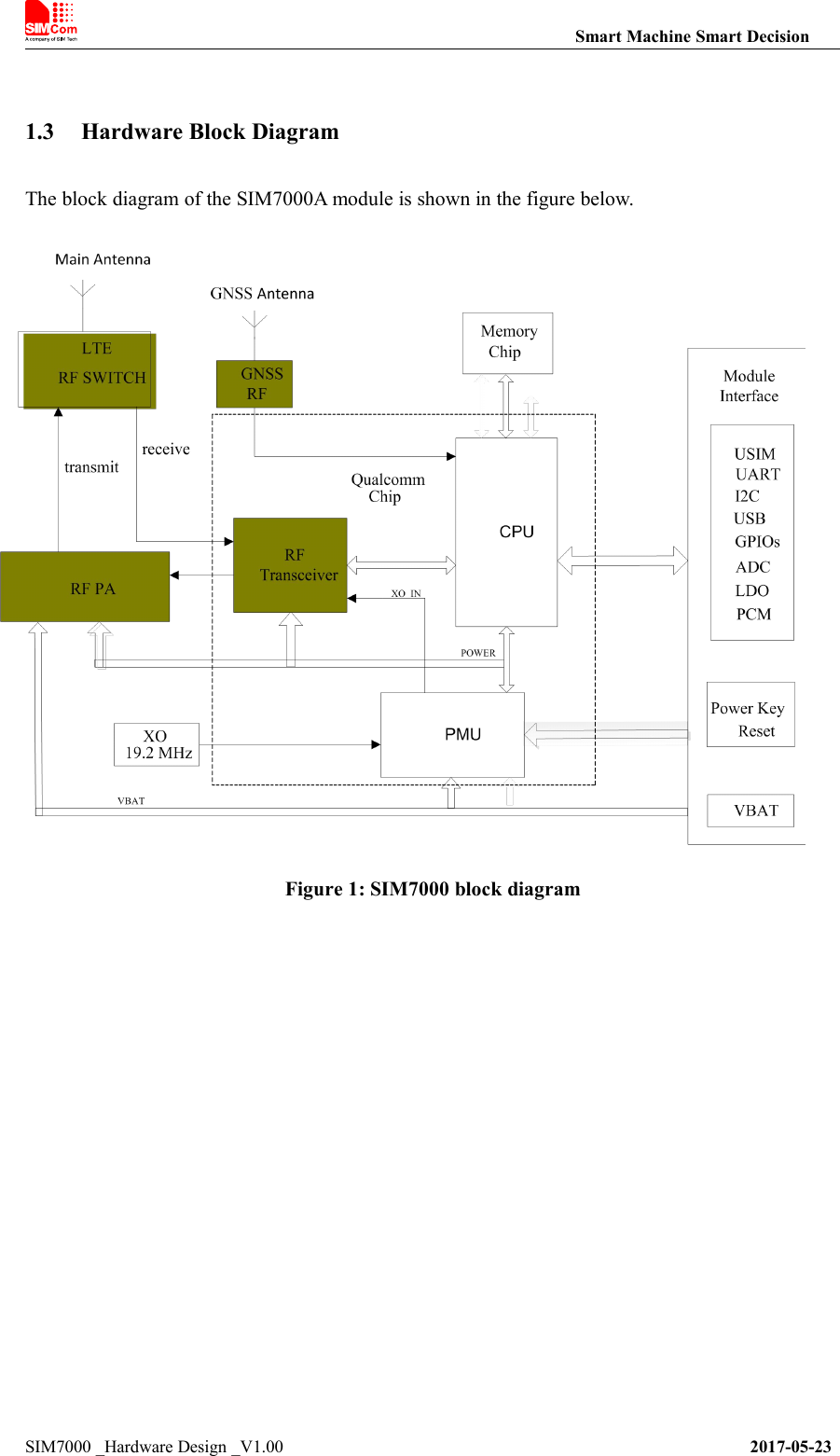
Smart Machine Smart DecisionSIM7000 _Hardware Design _V1.00 2017-05-231.3 Hardware Block DiagramThe block diagram of the SIM7000A module is shown in the figure below.Figure 1: SIM7000 block diagram
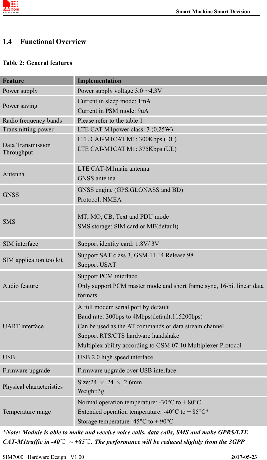
Smart Machine Smart DecisionSIM7000 _Hardware Design _V1.00 2017-05-231.4 Functional OverviewTable 2: General featuresFeatureImplementationPower supplyPower supply voltage 3.0~4.3VPower savingCurrent in sleep mode: 1mACurrent in PSM mode: 9uARadio frequency bandsPlease refer to the table 1Transmitting powerLTE CAT-M1power class: 3 (0.25W)Data TransmissionThroughputLTE CAT-M1CAT M1: 300Kbps (DL)LTE CAT-M1CAT M1: 375Kbps (UL)AntennaLTE CAT-M1main antenna. GNSS antennaGNSSGNSS engine (GPS,GLONASS and BD)Protocol: NMEASMSMT, MO, CB, Text and PDU modeSMS storage: SIM card or ME(default)SIM interfaceSupport identity card: 1.8V/ 3VSIM application toolkitSupport SAT class 3, GSM 11.14 Release 98Support USATAudio featureSupport PCM interfaceOnly support PCM master mode and short frame sync, 16-bit linear dataformatsUART interfaceA full modem serial port by defaultBaud rate: 300bps to 4Mbps(default:115200bps)Can be used as the AT commands or data stream channelSupport RTS/CTS hardware handshakeMultiplex ability according to GSM 07.10 Multiplexer ProtocolUSBUSB 2.0 high speed interfaceFirmware upgradeFirmware upgrade over USB interfacePhysical characteristicsSize:24 ×24 ×2.6mmWeight:3gTemperature rangeNormal operation temperature: -30°C to + 80°CExtended operation temperature: -40°C to + 85°C*Storage temperature -45°C to + 90°C*Note: Module is able to make and receive voice calls, data calls, SMS and make GPRS/LTECAT-M1traffic in -40℃~ +85℃. The performance will be reduced slightly from the 3GPP
Smart Machine Smart DecisionSIM7000 _Hardware Design _V1.00 2017-05-23specifications if the temperature is outside the normal operating temperature range and stillwithin the extreme operating temperature range.
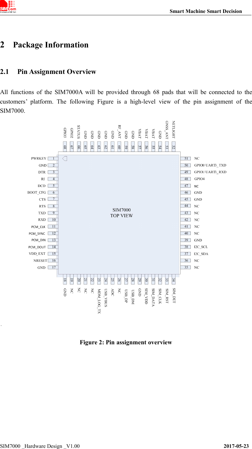
Smart Machine Smart DecisionSIM7000 _Hardware Design _V1.00 2017-05-232Package Information2.1 Pin Assignment OverviewAll functions of the SIM7000A will be provided through 68 pads that will be connected to thecustomers’ platform. The following Figure is a high-level view of the pin assignment of theSIM7000.Figure 2: Pin assignment overview
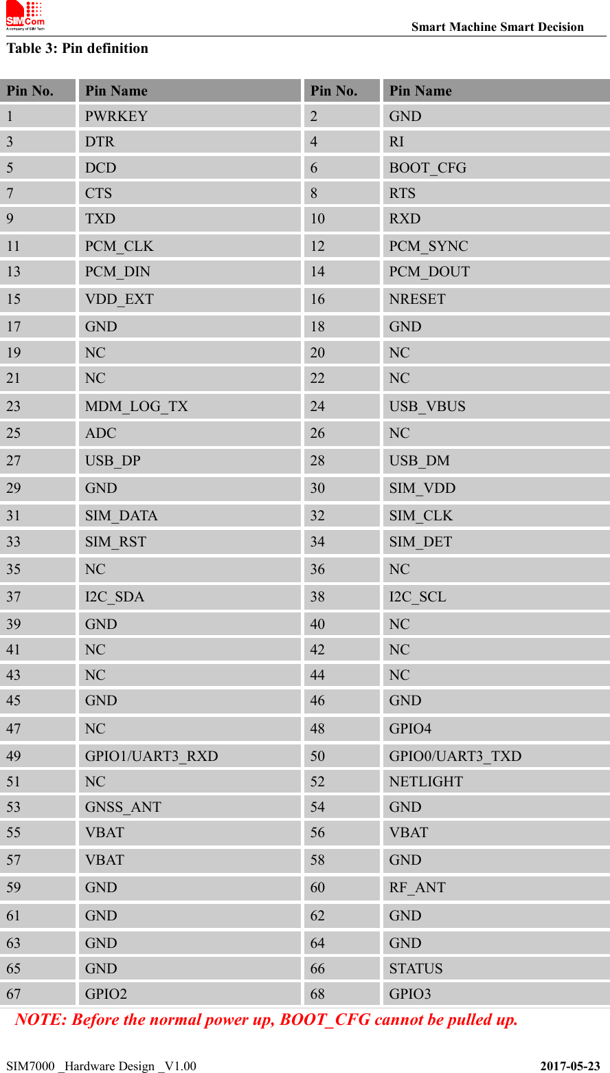
Smart Machine Smart DecisionSIM7000 _Hardware Design _V1.00 2017-05-23Table 3: Pin definitionPin No.Pin NamePin No.Pin Name1PWRKEY2GND3DTR4RI5DCD6BOOT_CFG7CTS8RTS9TXD10RXD11PCM_CLK12PCM_SYNC13PCM_DIN14PCM_DOUT15VDD_EXT16NRESET17GND18GND19NC20NC21NC22NC23MDM_LOG_TX24USB_VBUS25ADC26NC27USB_DP28USB_DM29GND30SIM_VDD31SIM_DATA32SIM_CLK33SIM_RST34SIM_DET35NC36NC37I2C_SDA38I2C_SCL39GND40NC41NC42NC43NC44NC45GND46GND47NC48GPIO449GPIO1/UART3_RXD50GPIO0/UART3_TXD51NC52NETLIGHT53GNSS_ANT54GND55VBAT56VBAT57VBAT58GND59GND60RF_ANT61GND62GND63GND64GND65GND66STATUS67GPIO268GPIO3NOTE: Before the normal power up, BOOT_CFG cannot be pulled up.
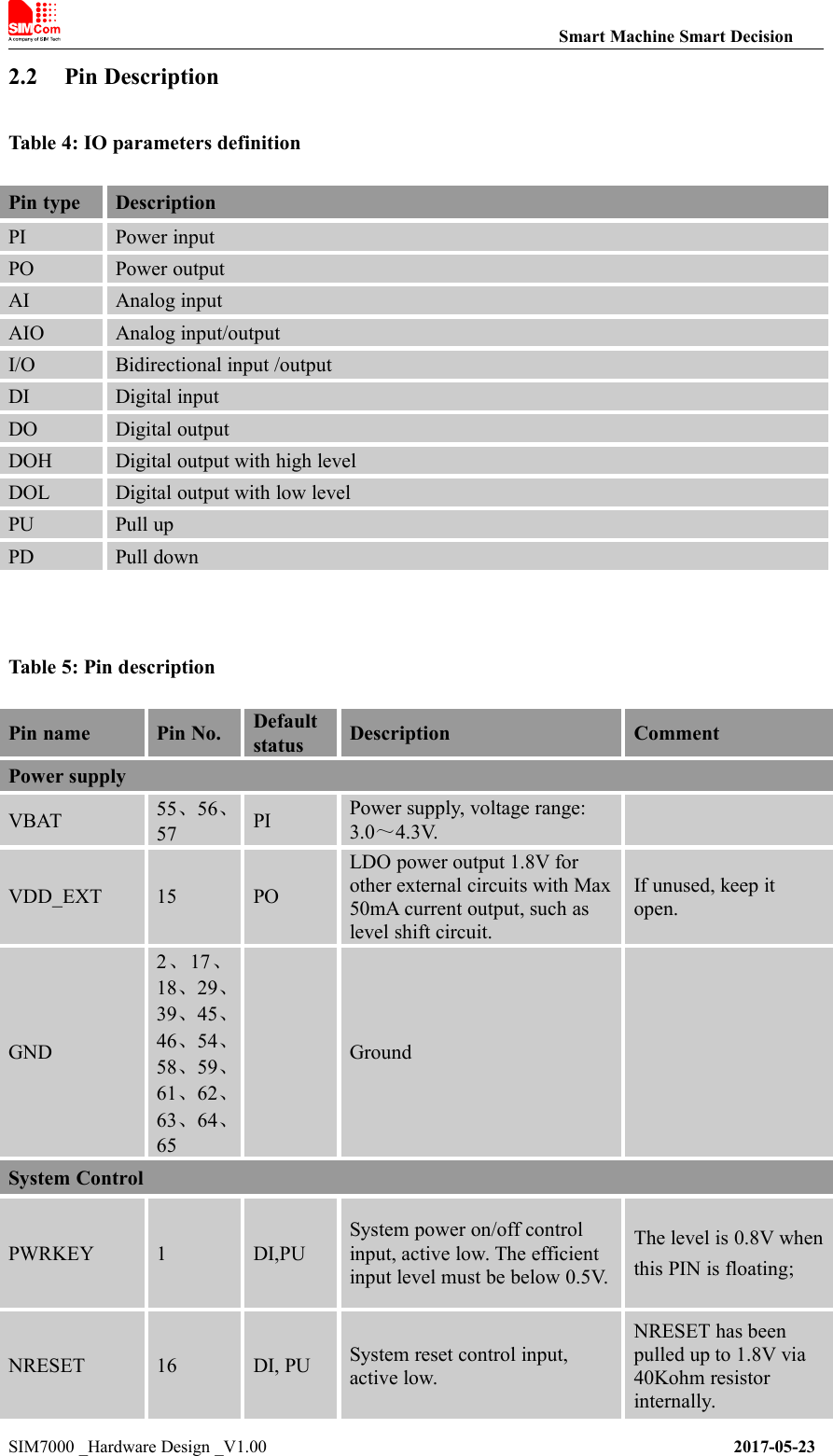
Smart Machine Smart DecisionSIM7000 _Hardware Design _V1.00 2017-05-232.2 Pin DescriptionTable 4: IO parameters definitionPin typeDescriptionPIPower inputPOPower outputAIAnalog inputAIOAnalog input/outputI/OBidirectional input /outputDIDigital inputDODigital outputDOHDigital output with high levelDOLDigital output with low levelPUPull upPDPull downTable 5: Pin descriptionPin namePin No.DefaultstatusDescriptionCommentPower supplyVBAT55、56、57PIPower supply, voltage range:3.0~4.3V.VDD_EXT15POLDO power output 1.8V forother external circuits with Max50mA current output, such aslevel shift circuit.If unused, keep itopen.GND2、17、18、29、39、45、46、54、58、59、61、62、63、64、65GroundSystem ControlPWRKEY1DI,PUSystem power on/off controlinput, active low. The efficientinput level must be below 0.5V.The level is 0.8V whenthis PIN is floating;NRESET16DI, PUSystem reset control input,active low.NRESET has beenpulled up to 1.8V via40Kohm resistorinternally.
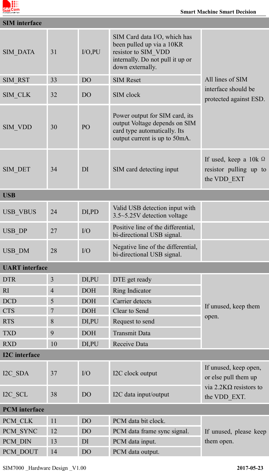
Smart Machine Smart DecisionSIM7000 _Hardware Design _V1.00 2017-05-23SIM interfaceSIM_DATA31I/O,PUSIM Card data I/O, which hasbeen pulled up via a 10KRresistor to SIM_VDDinternally. Do not pull it up ordown externally.All lines of SIMinterface should beprotected against ESD.SIM_RST33DOSIM ResetSIM_CLK32DOSIM clockSIM_VDD30POPower output for SIM card, itsoutput Voltage depends on SIMcard type automatically. Itsoutput current is up to 50mA.SIM_DET34DISIM card detecting inputIf used, keep a 10k Ωresistor pulling up tothe VDD_EXTUSBUSB_VBUS24DI,PDValid USB detection input with3.5~5.25V detection voltageUSB_DP27I/OPositive line of the differential,bi-directional USB signal.USB_DM28I/ONegative line of the differential,bi-directional USB signal.UART interfaceDTR3DI,PUDTE get readyIf unused, keep themopen.RI4DOHRing IndicatorDCD5DOHCarrier detectsCTS7DOHClear to SendRTS8DI,PURequest to sendTXD9DOHTransmit DataRXD10DI,PUReceive DataI2C interfaceI2C_SDA37I/OI2C clock outputIf unused, keep open,or else pull them upvia 2.2KΩ resistors tothe VDD_EXT.I2C_SCL38DOI2C data input/outputPCM interfacePCM_CLK11DOPCM data bit clock.If unused, please keepthem open.PCM_SYNC12DOPCM data frame sync signal.PCM_DIN13DIPCM data input.PCM_DOUT14DOPCM data output.
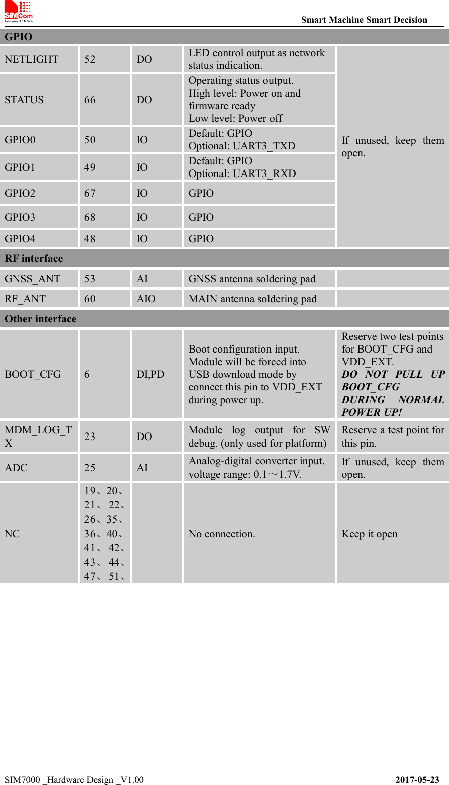
Smart Machine Smart DecisionSIM7000 _Hardware Design _V1.00 2017-05-23GPIONETLIGHT52DOLED control output as networkstatus indication.If unused, keep themopen.STATUS66DOOperating status output.High level: Power on andfirmware readyLow level: Power offGPIO050IODefault: GPIOOptional: UART3_TXDGPIO149IODefault: GPIOOptional: UART3_RXDGPIO267IOGPIOGPIO368IOGPIOGPIO448IOGPIORF interfaceGNSS_ANT53AIGNSS antenna soldering padRF_ANT60AIOMAIN antenna soldering padOther interfaceBOOT_CFG6DI,PDBoot configuration input.Module will be forced intoUSB download mode byconnect this pin to VDD_EXTduring power up.Reserve two test pointsfor BOOT_CFG andVDD_EXT.DO NOT PULL UPBOOT_CFGDURING NORMALPOWER UP!MDM_LOG_TX23DOModule log output for SWdebug. (only used for platform)Reserve a test point forthis pin.ADC25AIAnalog-digital converter input.voltage range: 0.1~1.7V.If unused, keep themopen.NC19、20、21、22、26、35、36、40、41、42、43、44、47、51、No connection.Keep it open
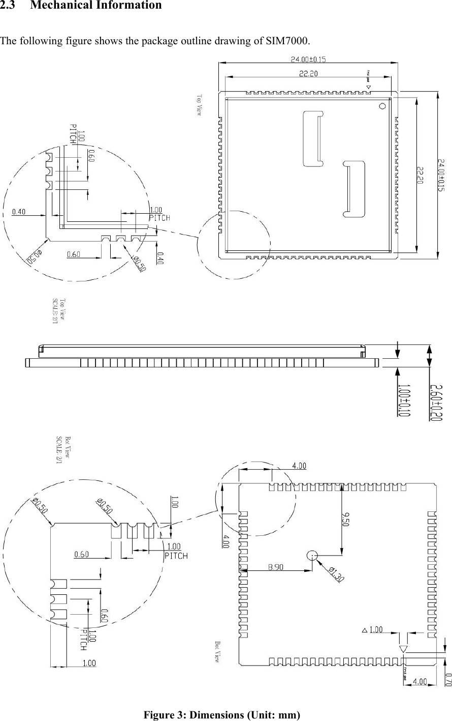
2.3 Mechanical InformationThe following figure shows the package outline drawing of SIM7000.Figure 3: Dimensions (Unit: mm)
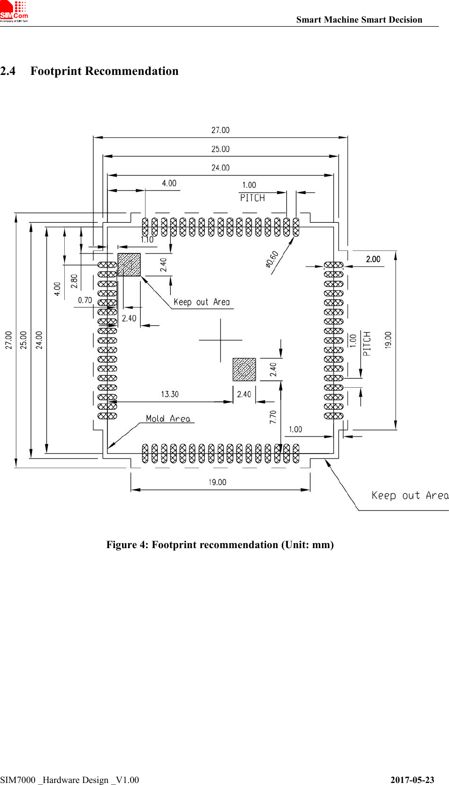
Smart Machine Smart DecisionSIM7000 _Hardware Design _V1.00 2017-05-232.4 Footprint RecommendationFigure 4: Footprint recommendation (Unit: mm)
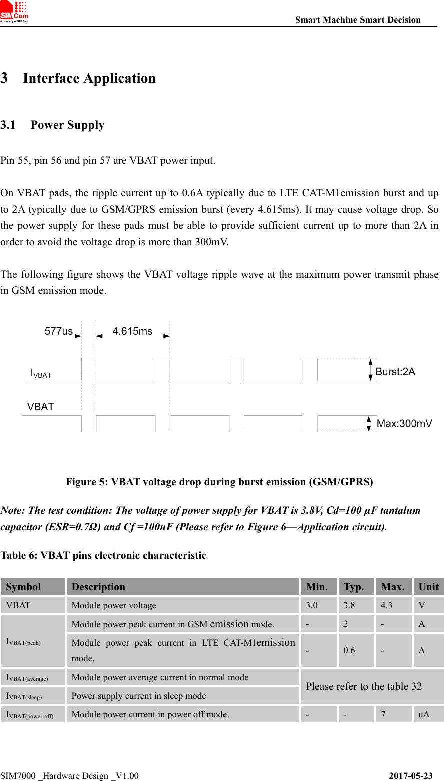
Smart Machine Smart DecisionSIM7000 _Hardware Design _V1.00 2017-05-233Interface Application3.1 Power SupplyPin 55, pin 56 and pin 57 are VBAT power input.On VBAT pads, the ripple current up to 0.6A typically due to LTE CAT-M1emission burst and upto 2A typically due to GSM/GPRS emission burst (every 4.615ms). It may cause voltage drop. Sothe power supply for these pads must be able to provide sufficient current up to more than 2A inorder to avoid the voltage drop is more than 300mV.The following figure shows the VBAT voltage ripple wave at the maximum power transmit phasein GSM emission mode.Figure 5: VBAT voltage drop during burst emission (GSM/GPRS)Note: The test condition: The voltage of power supply for VBAT is 3.8V, Cd=100 µF tantalumcapacitor (ESR=0.7Ω) and Cf =100nF (Please refer to Figure 6—Application circuit).Table 6: VBAT pins electronic characteristicSymbolDescriptionMin.Typ.Max.UnitVBATModule power voltage3.03.84.3VIVBAT(peak)Module power peak current in GSM emission mode.-2-AModule power peak current in LTE CAT-M1emissionmode.-0.6-AIVBAT(average)Module power average current in normal modePlease refer to the table 32IVBAT(sleep)Power supply current in sleep modeIVBAT(power-off)Module power current in power off mode.--7uA
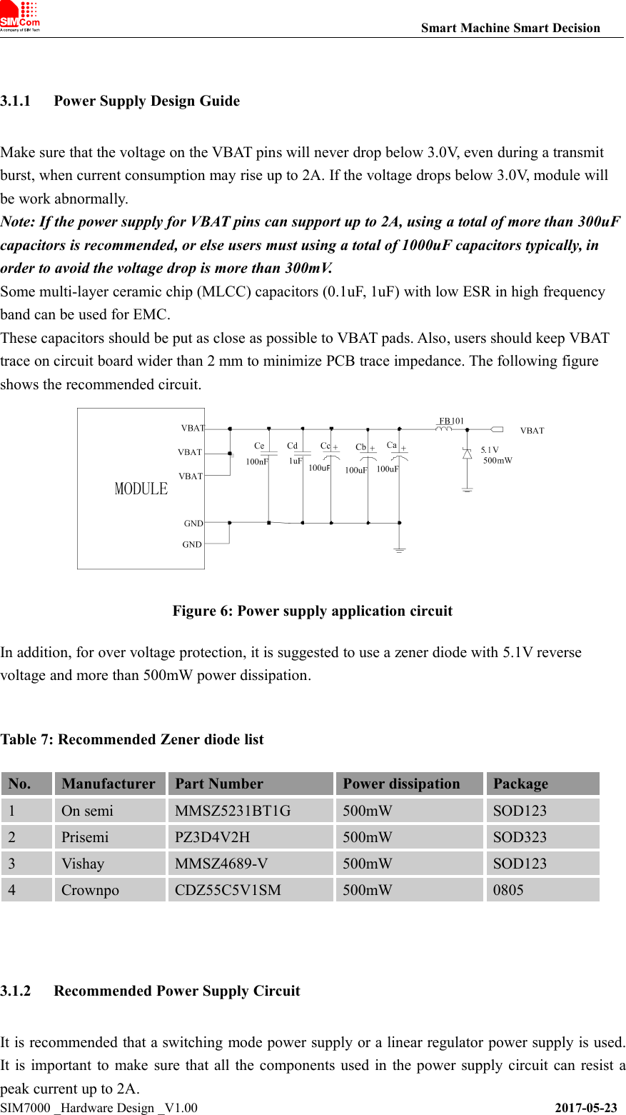
Smart Machine Smart DecisionSIM7000 _Hardware Design _V1.00 2017-05-233.1.1 Power Supply Design GuideMake sure that the voltage on the VBAT pins will never drop below 3.0V, even during a transmitburst, when current consumption may rise up to 2A. If the voltage drops below 3.0V, module willbe work abnormally.Note: If the power supply for VBAT pins can support up to 2A, using a total of more than 300uFcapacitors is recommended, or else users must using a total of 1000uF capacitors typically, inorder to avoid the voltage drop is more than 300mV.Some multi-layer ceramic chip (MLCC) capacitors (0.1uF, 1uF) with low ESR in high frequencyband can be used for EMC.These capacitors should be put as close as possible to VBAT pads. Also, users should keep VBATtrace on circuit board wider than 2 mm to minimize PCB trace impedance. The following figureshows the recommended circuit.Figure 6: Power supply application circuitIn addition, for over voltage protection, it is suggested to use a zener diode with 5.1V reversevoltage and more than 500mW power dissipation.Table 7: Recommended Zener diode listNo.ManufacturerPart NumberPower dissipationPackage1On semiMMSZ5231BT1G500mWSOD1232PrisemiPZ3D4V2H500mWSOD3233VishayMMSZ4689-V500mWSOD1234CrownpoCDZ55C5V1SM500mW08053.1.2 Recommended Power Supply CircuitIt is recommended that a switching mode power supply or a linear regulator power supply is used.It is important to make sure that all the components used in the power supply circuit can resist apeak current up to 2A.
Smart Machine Smart DecisionSIM7000 _Hardware Design _V1.00 2017-05-23The following figure shows the linear regulator reference circuit with 5V input and 3.8V output.Figure 7: Linear regulator reference circuitIf there is a big voltage difference between input and output for VBAT power supply, or theefficiency is extremely important, then a switching mode power supply will be preferable. Thefollowing figure shows the switching mode power supply reference circuit.Figure 8: Switching mode power supply reference circuitNote: The Switching Mode power supply solution for VBAT must be chosen carefully againstElectro Magnetic Interference and ripple current from depraving RF performance.3.1.3 Voltage MonitorTo monitor the VBAT voltage, the AT command “AT+CBC” can be used.To monitor whether the VBAT voltage is inside a special range, the AT command“AT+CBATCHK” can be used to enable the overvoltage warning function and the under-voltagewarning function. The default value of the overvoltage warning function in the software is 4.3V,and the default value of the under-voltage warning function is 3.1V.When the VBAT voltage is out of the range, the module will be power off. If users need to poweroff SIM7000 when the VBAT voltage is out of the range, the AT command “AT+CBATCHK” canbe used to enable the overvoltage power-off function and the under-voltage power-off function. Thedefault value of the overvoltage power-off function in the software is 4.4V, and the default value ofthe under-voltage power-off function is 2.9V.Note: Under-voltage warning function and under-voltage power-off function are disabled bydefault. For more information about these AT commands, please refer to Document [1].
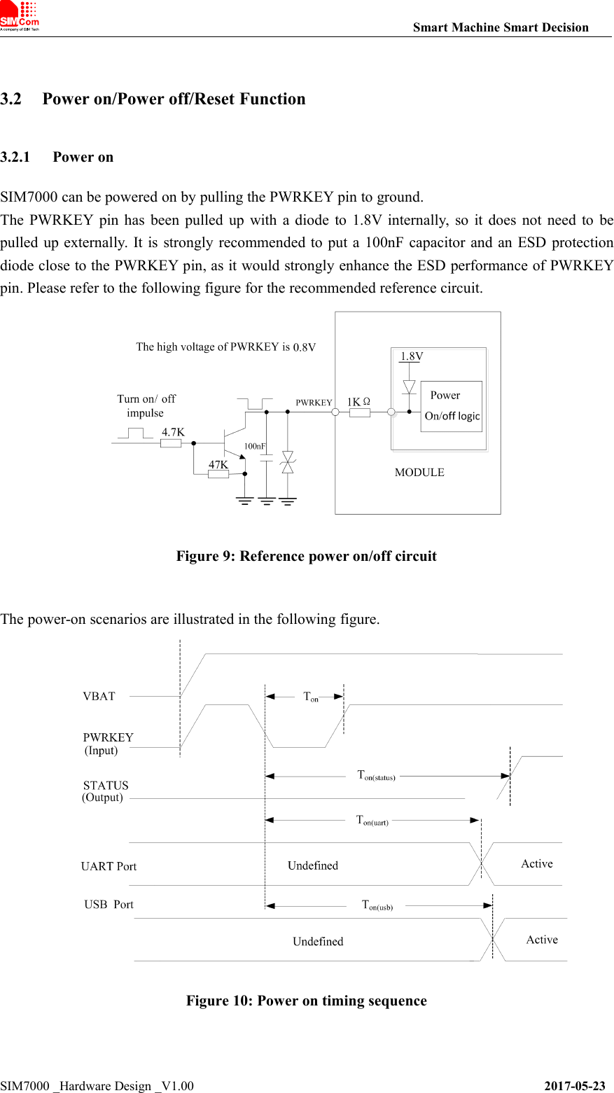
Smart Machine Smart DecisionSIM7000 _Hardware Design _V1.00 2017-05-233.2 Power on/Power off/Reset Function3.2.1 Power onSIM7000 can be powered on by pulling the PWRKEY pin to ground.The PWRKEY pin has been pulled up with a diode to 1.8V internally, so it does not need to bepulled up externally. It is strongly recommended to put a 100nF capacitor and an ESD protectiondiode close to the PWRKEY pin, as it would strongly enhance the ESD performance of PWRKEYpin. Please refer to the following figure for the recommended reference circuit.Figure 9: Reference power on/off circuitThe power-on scenarios are illustrated in the following figure.Figure 10: Power on timing sequence
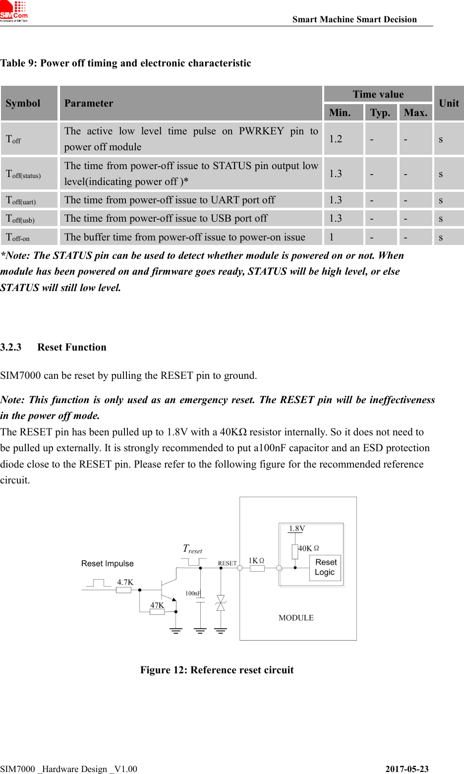
Smart Machine Smart DecisionSIM7000 _Hardware Design _V1.00 2017-05-23Table 8: Power on timing and electronic characteristicSymbolParameterMin.Typ.Max.UnitTonThe time of active low level impulse of PWRKEYpin to power on module72--msTon(status)The time from power-on issue to STATUS pinoutput high level(indicating power up ready )4.2--sTon(uart)The time from power-on issue to UART port ready3.5--sTon(usb)The time from power-on issue to USB port ready3.5--sVIHInput high level voltage on PWRKEY pin0.60.81.8VVILInput low level voltage on PWRKEY pin-0.300.5V3.2.2 Power offThe following methods can be used to power off SIM7000.●Method 1: Power off SIM7000 by pulling the PWRKEY pin to ground.●Method 2: Power off SIM7000 by AT command “AT+CPOWD”.●Method 3: over-voltage or under-voltage automatic power off. The voltage range can be set byAT command “AT+CBATCHK”.●Method 4: over-temperature or under-temperature automatic power off.Note: If the temperature is outside the range of -30~+80℃, some warning will be reported viaAT port. If the temperature is outside the range of -40~+85℃, SIM7000 will be powered offautomatically.For details about “AT+CPOWD” and “AT+CBATCHK”, please refer to Document [1].These procedures will make modules disconnect from the network and allow the software to enter asafe state, and save data before module be powered off completely.The power off scenario by pulling down the PWRKEY pin is illustrated in the following figure.Figure 11: Power off timing sequence
Smart Machine Smart DecisionSIM7000 _Hardware Design _V1.00 2017-05-23Table 9: Power off timing and electronic characteristicSymbolParameterTime valueUnitMin.Typ.Max.ToffThe active low level time pulse on PWRKEY pin topower off module1.2--sToff(status)The time from power-off issue to STATUS pin output lowlevel(indicating power off )*1.3--sToff(uart)The time from power-off issue to UART port off1.3--sToff(usb)The time from power-off issue to USB port off1.3--sToff-onThe buffer time from power-off issue to power-on issue1--s*Note: The STATUS pin can be used to detect whether module is powered on or not. Whenmodule has been powered on and firmware goes ready, STATUS will be high level, or elseSTATUS will still low level.3.2.3 Reset FunctionSIM7000 can be reset by pulling the RESET pin to ground.Note: This function is only used as an emergency reset. The RESET pin will be ineffectivenessin the power off mode.The RESET pin has been pulled up to 1.8V with a 40KΩ resistor internally. So it does not need tobe pulled up externally. It is strongly recommended to put a100nF capacitor and an ESD protectiondiode close to the RESET pin. Please refer to the following figure for the recommended referencecircuit.Figure 12: Reference reset circuit
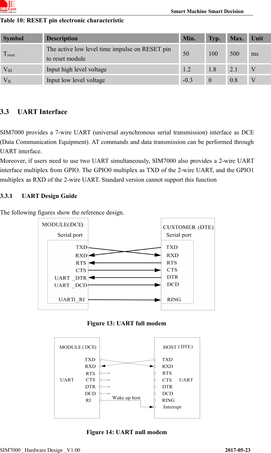
Smart Machine Smart DecisionSIM7000 _Hardware Design _V1.00 2017-05-23Table 10: RESET pin electronic characteristicSymbolDescriptionMin.Typ.Max.UnitTresetThe active low level time impulse on RESET pinto reset module50100500msVIHInput high level voltage1.21.82.1VVILInput low level voltage-0.300.8V3.3 UART InterfaceSIM7000 provides a 7-wire UART (universal asynchronous serial transmission) interface as DCE(Data Communication Equipment). AT commands and data transmission can be performed throughUART interface.Moreover, if users need to use two UART simultaneously, SIM7000 also provides a 2-wire UARTinterface multiplex from GPIO. The GPIO0 multiplex as TXD of the 2-wire UART, and the GPIO1multiplex as RXD of the 2-wire UART. Standard version cannot support this function3.3.1 UART Design GuideThe following figures show the reference design.Figure 13: UART full modemFigure 14: UART null modem
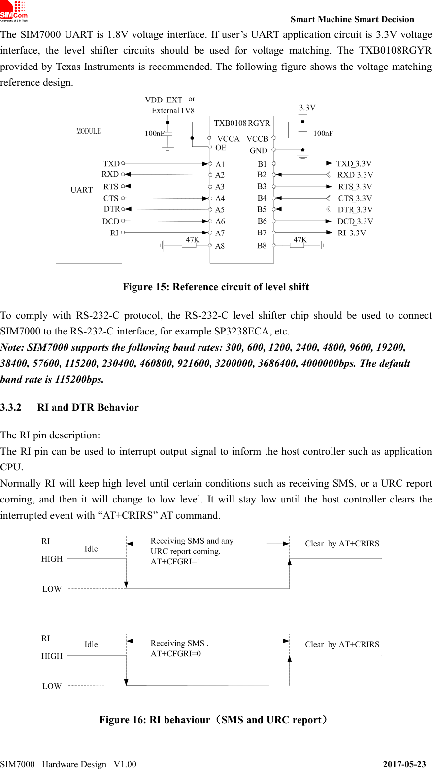
Smart Machine Smart DecisionSIM7000 _Hardware Design _V1.00 2017-05-23The SIM7000 UART is 1.8V voltage interface. If user’s UART application circuit is 3.3V voltageinterface, the level shifter circuits should be used for voltage matching. The TXB0108RGYRprovided by Texas Instruments is recommended. The following figure shows the voltage matchingreference design.Figure 15: Reference circuit of level shiftTo comply with RS-232-C protocol, the RS-232-C level shifter chip should be used to connectSIM7000 to the RS-232-C interface, for example SP3238ECA, etc.Note: SIM7000 supports the following baud rates: 300, 600, 1200, 2400, 4800, 9600, 19200,38400, 57600, 115200, 230400, 460800, 921600, 3200000, 3686400, 4000000bps. The defaultband rate is 115200bps.3.3.2 RI and DTR BehaviorThe RI pin description:The RI pin can be used to interrupt output signal to inform the host controller such as applicationCPU.Normally RI will keep high level until certain conditions such as receiving SMS, or a URC reportcoming, and then it will change to low level. It will stay low until the host controller clears theinterrupted event with “AT+CRIRS” AT command.Figure 16: RI behaviour(SMS and URC report)
Smart Machine Smart DecisionSIM7000 _Hardware Design _V1.00 2017-05-23Normally RI will be kept at a high level until a voice call, then it will output periodic rectangularwave with 5900ms low level and 100ms high level. It will output this kind of periodic rectangularwave until the call is answered or hung up.Figure 17: RI behaviour(voice call)Note: For more details of AT commands about UART, please refer to document [1] and [22].The DTR pin description:After setting the AT command “AT+CSCLK=1”, SIM7000 will enter sleep mode by pulling up theDTR pin when module is in the idle mode. In sleep mode, the UART is unavailable. WhenSIM7000 enters sleep mode, pulling down DTR can wake up module.3.4 USB InterfaceThe SIM7000 contains a USB interface compliant with the USB2.0 specification as a peripheral,but the USB charging function is not supported.SIM7000 supports the USB suspend and resume mechanism which can reduce power consumption.If there is no data transmission on the USB bus, SIM7000 will enter suspend mode automatically,and will be resumed by some events such as voice call, receiving SMS, etc.Figure 18: USB reference circuitBecause of the high speed on USB bus, more attention should be paid to the influence of thejunction capacitance of the ESD component on USB data lines. Typically, the capacitance of the D1and D2 should be less than 1pF.D3 is suggested to select the diode with anti-ESD and voltage surge function, or customer couldadd a ZENER diode for surge clamping.Note:The USB_DM and USB_DP nets must be traced by 90Ohm+/-10% differential impedance.
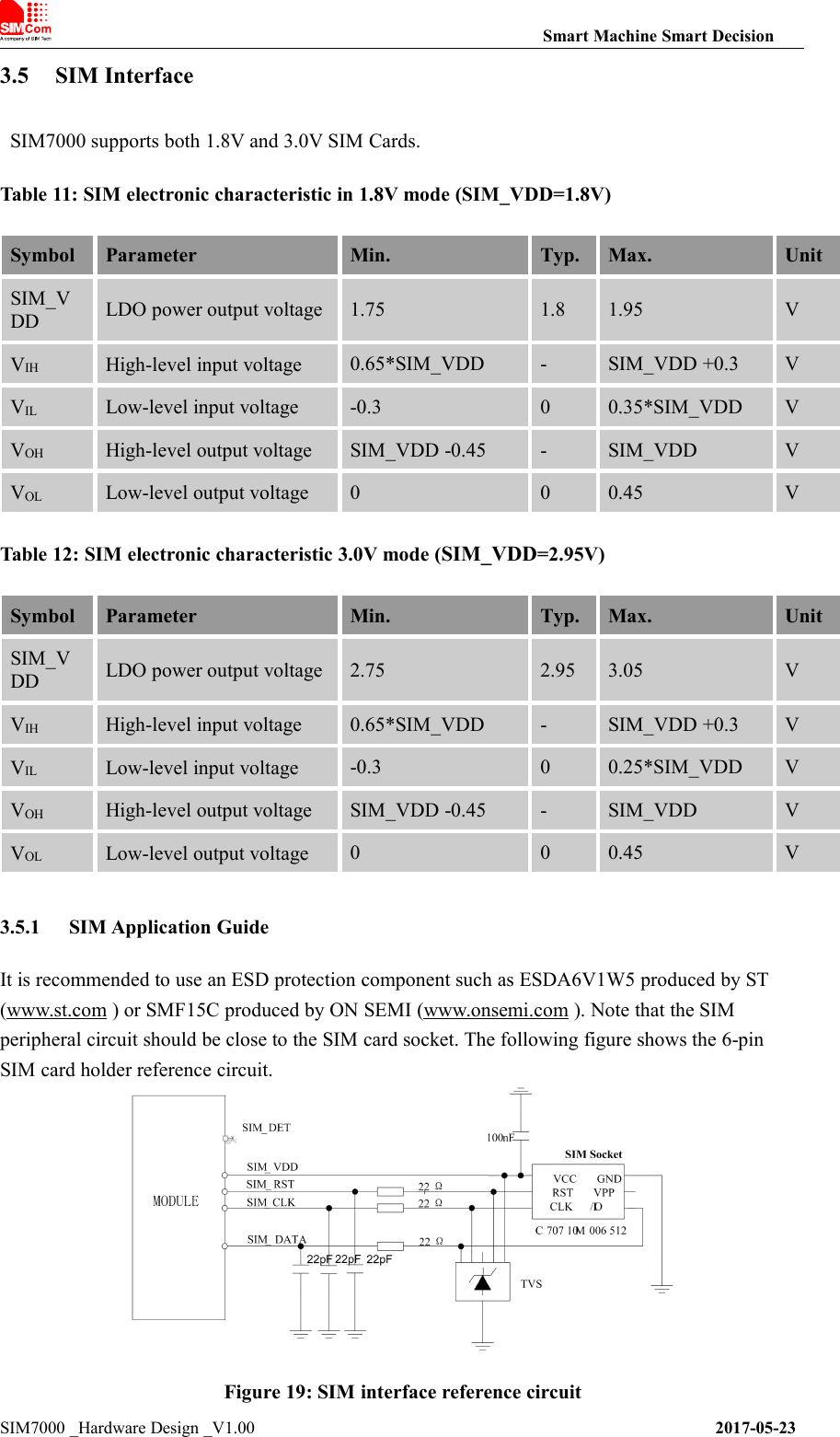
Smart Machine Smart DecisionSIM7000 _Hardware Design _V1.00 2017-05-233.5 SIM InterfaceSIM7000 supports both 1.8V and 3.0V SIM Cards.Table 11: SIM electronic characteristic in 1.8V mode (SIM_VDD=1.8V)SymbolParameterMin.Typ.Max.UnitSIM_VDDLDO power output voltage1.751.81.95VVIHHigh-level input voltage0.65*SIM_VDD-SIM_VDD +0.3VVILLow-level input voltage-0.300.35*SIM_VDDVVOHHigh-level output voltageSIM_VDD -0.45-SIM_VDDVVOLLow-level output voltage000.45VTable 12: SIM electronic characteristic 3.0V mode (SIM_VDD=2.95V)SymbolParameterMin.Typ.Max.UnitSIM_VDDLDO power output voltage2.752.953.05VVIHHigh-level input voltage0.65*SIM_VDD-SIM_VDD +0.3VVILLow-level input voltage-0.300.25*SIM_VDDVVOHHigh-level output voltageSIM_VDD -0.45-SIM_VDDVVOLLow-level output voltage000.45V3.5.1 SIM Application GuideIt is recommended to use an ESD protection component such as ESDA6V1W5 produced by ST(www.st.com ) or SMF15C produced by ON SEMI (www.onsemi.com ). Note that the SIMperipheral circuit should be close to the SIM card socket. The following figure shows the 6-pinSIM card holder reference circuit.Figure 19: SIM interface reference circuit
Smart Machine Smart DecisionSIM7000 _Hardware Design _V1.00 2017-05-23Note: SIM_DATA has been pulled up with a 10KΩ resistor to SIM_VDD in module. A 100nFcapacitor on SIM_VDD is used to reduce interference. For more details of AT commands aboutSIM, please refer to document [1].SIM_CLK is very important signal, the rise time and fall timeof SIM_CLK should be less than 40ns, otherwise the SIM card might not be initialized correctly.If SIM_DET is used, a 10KΩ resistor is necessary to pulling up to the power VDD_EXT.3.5.2 Recommended SIM Card HolderIt is recommended to use the 6-pin SIM socket such as C707 10M006 512 produced by Amphenol.User can visit http://www.amphenol.com for more information about the holder.Figure 20: Amphenol SIM card socketTable 13: Amphenol SIM socket pin descriptionPinSignalDescriptionC1SIM_VDDSIM Card Power supply.C2SIM_RSTSIM Card Reset.C3SIM_CLKSIM Card Clock.C5GNDConnect to GND.C6VPPC7SIM_DATASIM Card data I/O.
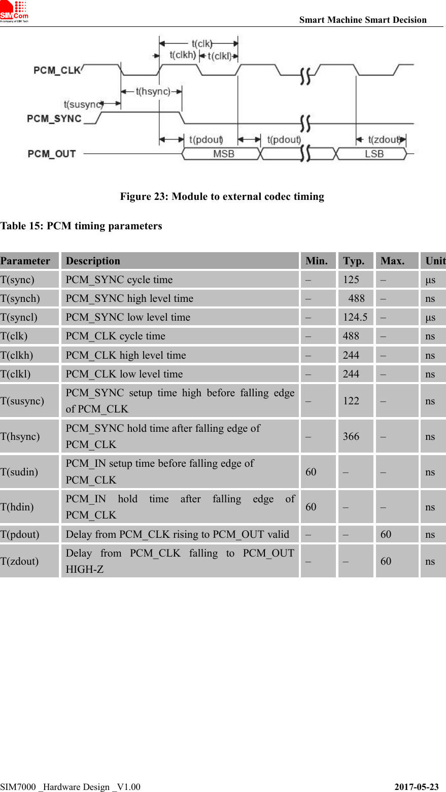
3.6 PCM InterfaceSIM7000 provides a PCM interface for external codec, which can be used in master mode withshort sync and 16 bits linear format.Table 14: PCM formatNote: For more details about PCM AT commands, please refer to document [1].3.6.1 PCM timingSIM7000 supports 2.048 MHz PCM data and sync timing for 16 bits linear format codec.Figure 21: PCM_SYNC timingFigure 22: External codec to module timingCharacteristicsSpecificationLine Interface FormatLinear(Fixed)Data length16bits(Fixed)PCM Clock/Sync SourceMaster Mode(Fixed)PCM Clock Rate2048 KHz (Fixed)PCM Sync FormatShort sync(Fixed)Data OrderingMSB
Smart Machine Smart DecisionSIM7000 _Hardware Design _V1.00 2017-05-23Figure 23: Module to external codec timingTable 15: PCM timing parametersParameterDescriptionMin.Typ.Max.UnitT(sync)PCM_SYNC cycle time–125–μsT(synch)PCM_SYNC high level time–488–nsT(syncl)PCM_SYNC low level time–124.5–μsT(clk)PCM_CLK cycle time–488–nsT(clkh)PCM_CLK high level time–244–nsT(clkl)PCM_CLK low level time–244–nsT(susync)PCM_SYNC setup time high before falling edgeof PCM_CLK–122–nsT(hsync)PCM_SYNC hold time after falling edge ofPCM_CLK–366–nsT(sudin)PCM_IN setup time before falling edge ofPCM_CLK60––nsT(hdin)PCM_IN hold time after falling edge ofPCM_CLK60––nsT(pdout)Delay from PCM_CLK rising to PCM_OUT valid––60nsT(zdout)Delay from PCM_CLK falling to PCM_OUTHIGH-Z––60ns
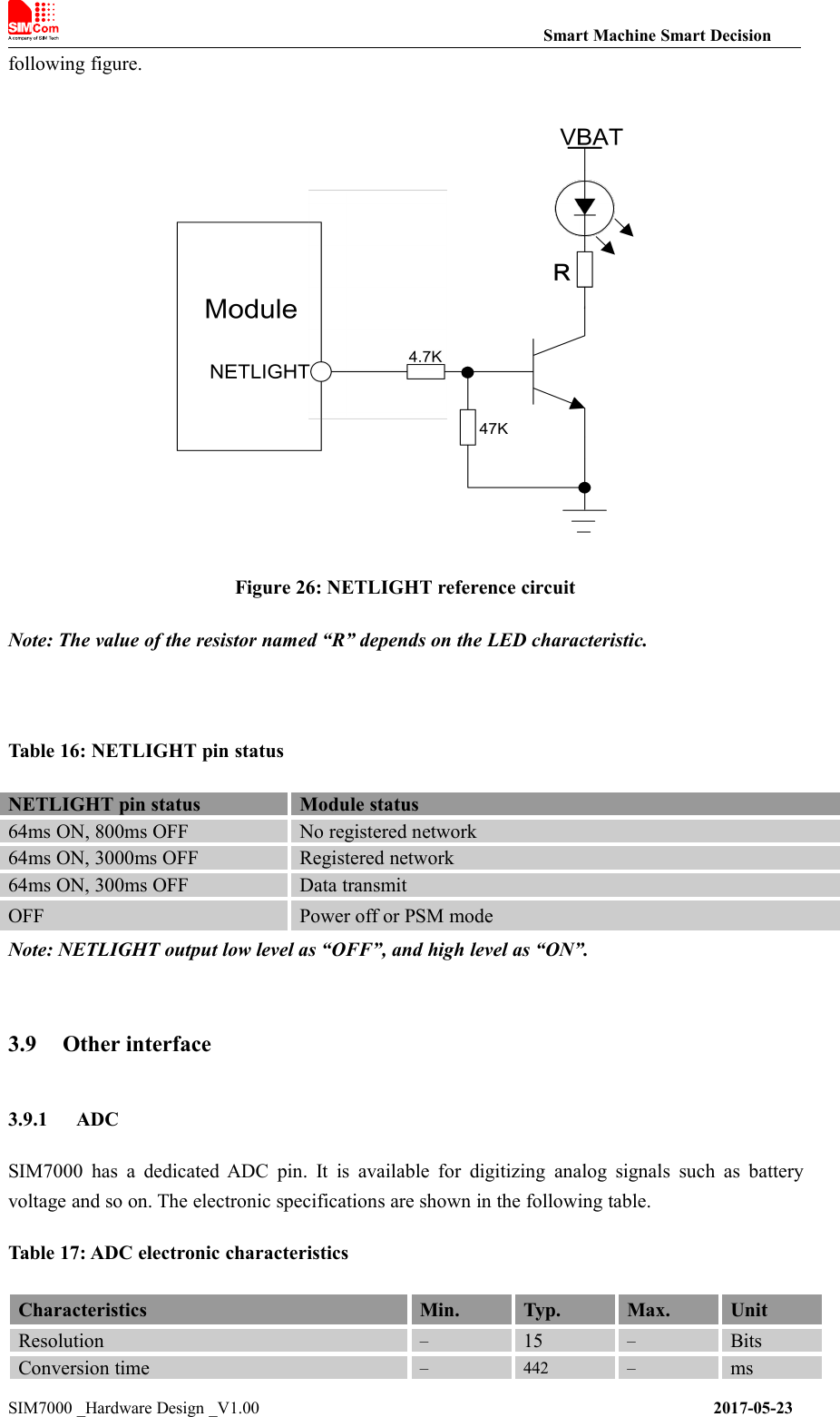
Smart Machine Smart DecisionSIM7000 _Hardware Design _V1.00 2017-05-233.6.2 PCM Application GuideThe following figure shows the external codec reference design.Figure 24: Audio codec reference circuit3.7 I2C InterfaceSIM7000 provides a I2C interface compatible with I2C specification, version 5.0, with clock rateup to 400 kbps. Its operation voltage is 1.8V.The following figure shows the I2C bus reference design.Figure 25: I2C reference circuitNote:I2C_SDA and I2C_SCL do not have pull-up resistors in module. So the two externalpulling up resistors are needed in application circuit.“AT+CRIIC and AT+CWIIC” AT commands could be used to read/write register values of theI2C peripheral devices. For more details about AT commands please refer to document [1].3.8 Network statusThe NETLIGHT pin is used to control Network Status LED, its reference circuit is shown in the
Smart Machine Smart DecisionSIM7000 _Hardware Design _V1.00 2017-05-23following figure.Figure 26: NETLIGHT reference circuitNote: The value of the resistor named “R” depends on the LED characteristic.Table 16: NETLIGHT pin statusNETLIGHT pin statusModule status64ms ON, 800ms OFFNo registered network64ms ON, 3000ms OFFRegistered network64ms ON, 300ms OFFData transmitOFFPower off or PSM modeNote: NETLIGHT output low level as “OFF”, and high level as “ON”.3.9 Other interface3.9.1 ADCSIM7000 has a dedicated ADC pin. It is available for digitizing analog signals such as batteryvoltage and so on. The electronic specifications are shown in the following table.Table 17: ADC electronic characteristicsCharacteristicsMin.Typ.Max.UnitResolution–15–BitsConversion time–442–ms
Smart Machine Smart DecisionSIM7000 _Hardware Design _V1.00 2017-05-23Input Range0.11.7VInput serial resistance1––MΩNote: “AT+CADC” can be used to read the voltage of the ADC pin, for more details, please referto document [1].3.9.2 LDOSIM7000 has a LDO power output named VDD_EXT. The output voltage is 1.8V.Figure 27:Power on sequence of the VDD_EXTTable 18: Electronic characteristicSymbolDescriptionMin.Typ.Max.UnitVVDD_EXTOutput voltage1.71.81.9VIOOutput current--50mANote:The VDD_EXT is used to the IO power in the module. The Output voltage is not supportedto set.
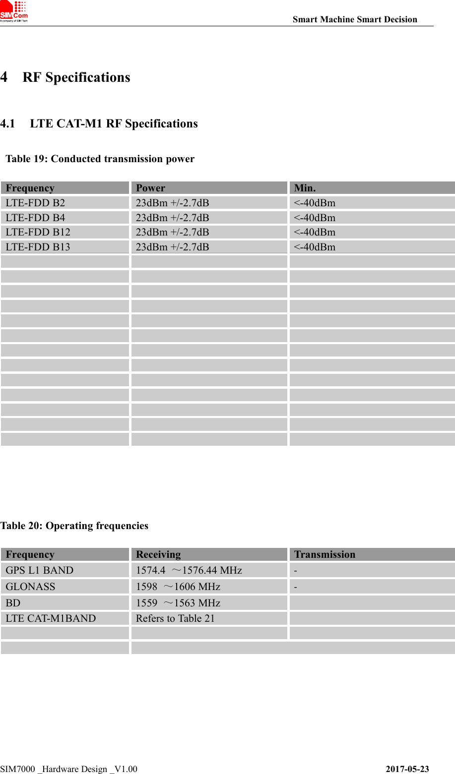
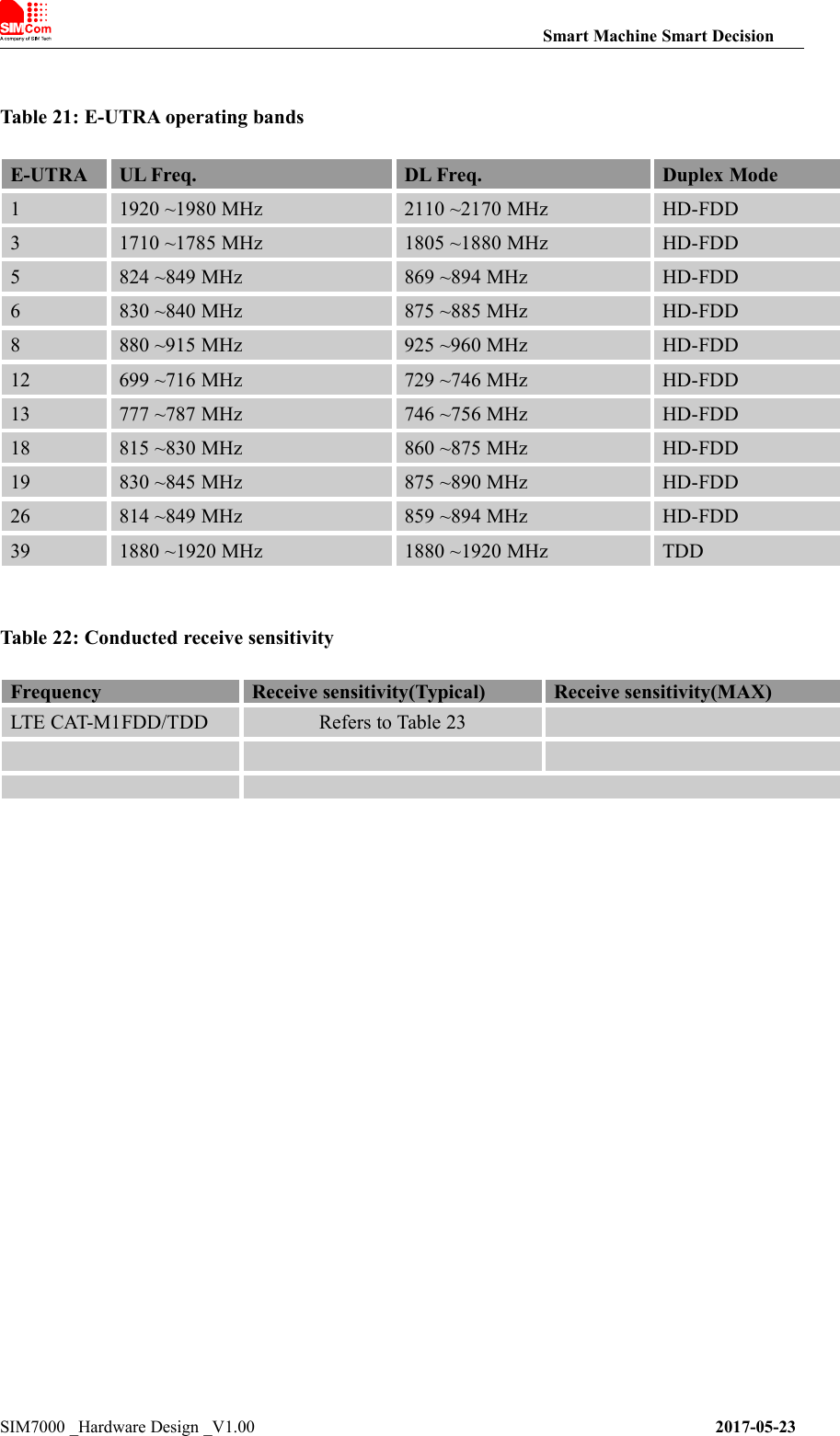
Smart Machine Smart DecisionSIM7000 _Hardware Design _V1.00 2017-05-234RF Specifications4.1 LTE CAT-M1 RF SpecificationsTable 19: Conducted transmission powerFrequencyPowerMin.LTE-FDD B223dBm +/-2.7dB<-40dBmLTE-FDD B423dBm +/-2.7dB<-40dBmLTE-FDD B1223dBm +/-2.7dB<-40dBmLTE-FDD B1323dBm +/-2.7dB<-40dBmTable 20: Operating frequenciesFrequencyReceivingTransmissionGPS L1 BAND1574.4 ~1576.44 MHz-GLONASS1598 ~1606 MHz-BD1559 ~1563 MHzLTE CAT-M1BANDRefers to Table 21
Smart Machine Smart DecisionSIM7000 _Hardware Design _V1.00 2017-05-23Table 21: E-UTRA operating bandsE-UTRAUL Freq.DL Freq.Duplex Mode11920 ~1980 MHz2110 ~2170 MHzHD-FDD31710 ~1785 MHz1805 ~1880 MHzHD-FDD5824 ~849 MHz869 ~894 MHzHD-FDD6830 ~840 MHz875 ~885 MHzHD-FDD8880 ~915 MHz925 ~960 MHzHD-FDD12699 ~716 MHz729 ~746 MHzHD-FDD13777 ~787 MHz746 ~756 MHzHD-FDD18815 ~830 MHz860 ~875 MHzHD-FDD19830 ~845 MHz875 ~890 MHzHD-FDD26814 ~849 MHz859 ~894 MHzHD-FDD391880 ~1920 MHz1880 ~1920 MHzTDDTable 22: Conducted receive sensitivityFrequencyReceive sensitivity(Typical)Receive sensitivity(MAX)LTE CAT-M1FDD/TDDRefers to Table 23
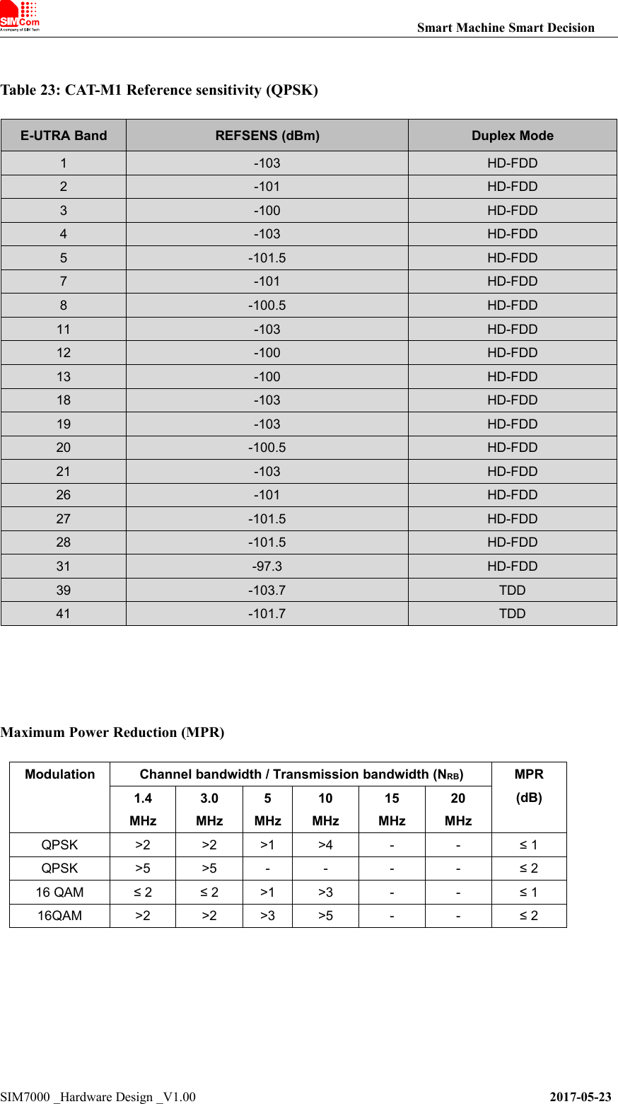
Smart Machine Smart DecisionSIM7000 _Hardware Design _V1.00 2017-05-23Table 23: CAT-M1 Reference sensitivity (QPSK)E-UTRA BandREFSENS (dBm)Duplex Mode1-103HD-FDD2-101HD-FDD3-100HD-FDD4-103HD-FDD5-101.5HD-FDD7-101HD-FDD8-100.5HD-FDD11-103HD-FDD12-100HD-FDD13-100HD-FDD18-103HD-FDD19-103HD-FDD20-100.5HD-FDD21-103HD-FDD26-101HD-FDD27-101.5HD-FDD28-101.5HD-FDD31-97.3HD-FDD39-103.7TDD41-101.7TDDMaximum Power Reduction (MPR)ModulationChannel bandwidth / Transmission bandwidth (NRB)MPR(dB)1.4MHz3.0MHz5MHz10MHz15MHz20MHzQPSK>2>2>1>4--≤ 1QPSK>5>5----≤ 216 QAM≤ 2≤ 2>1>3--≤ 116QAM>2>2>3>5--≤ 2
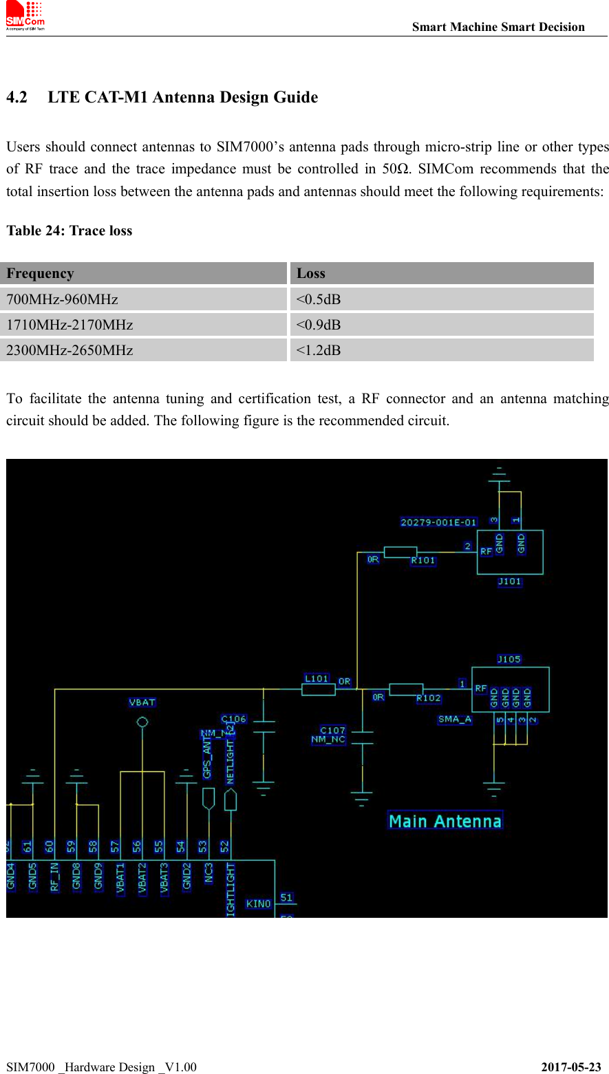
Smart Machine Smart DecisionSIM7000 _Hardware Design _V1.00 2017-05-234.2 LTE CAT-M1 Antenna Design GuideUsers should connect antennas to SIM7000’s antenna pads through micro-strip line or other typesof RF trace and the trace impedance must be controlled in 50Ω. SIMCom recommends that thetotal insertion loss between the antenna pads and antennas should meet the following requirements:Table 24: Trace lossFrequencyLoss700MHz-960MHz<0.5dB1710MHz-2170MHz<0.9dB2300MHz-2650MHz<1.2dBTo facilitate the antenna tuning and certification test, a RF connector and an antenna matchingcircuit should be added. The following figure is the recommended circuit.
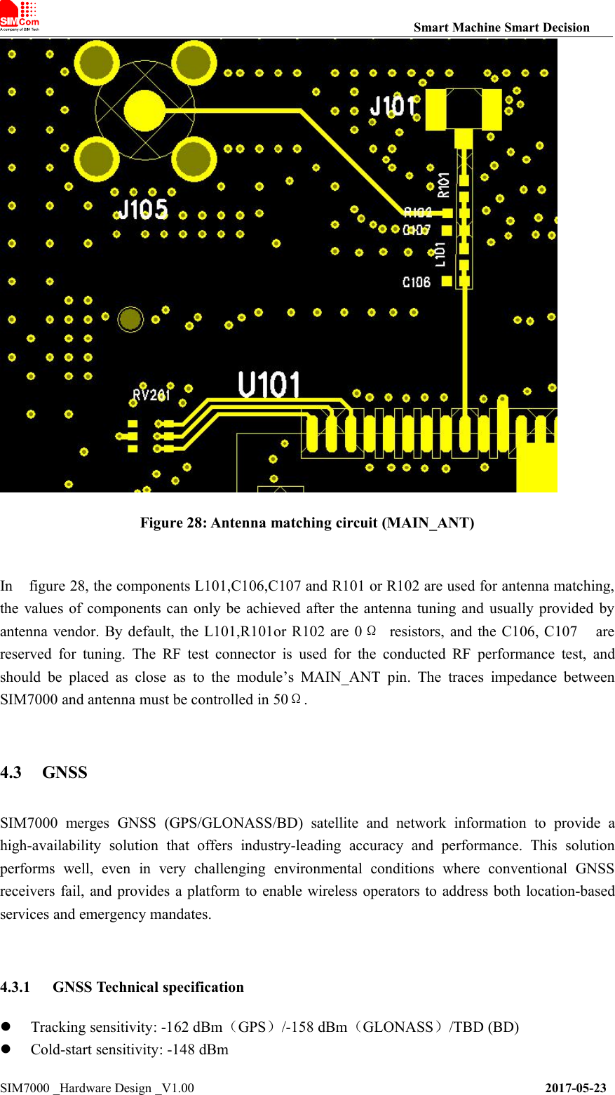
Smart Machine Smart DecisionSIM7000 _Hardware Design _V1.00 2017-05-23Figure 28: Antenna matching circuit (MAIN_ANT)In figure 28, the components L101,C106,C107 and R101 or R102 are used for antenna matching,the values of components can only be achieved after the antenna tuning and usually provided byantenna vendor. By default, the L101,R101or R102 are 0 Ωresistors, and the C106, C107 arereserved for tuning. The RF test connector is used for the conducted RF performance test, andshould be placed as close as to the module’s MAIN_ANT pin. The traces impedance betweenSIM7000 and antenna must be controlled in 50Ω.4.3 GNSSSIM7000 merges GNSS (GPS/GLONASS/BD) satellite and network information to provide ahigh-availability solution that offers industry-leading accuracy and performance. This solutionperforms well, even in very challenging environmental conditions where conventional GNSSreceivers fail, and provides a platform to enable wireless operators to address both location-basedservices and emergency mandates.4.3.1 GNSS Technical specificationTracking sensitivity: -162 dBm(GPS)/-158 dBm(GLONASS)/TBD (BD)Cold-start sensitivity: -148 dBm
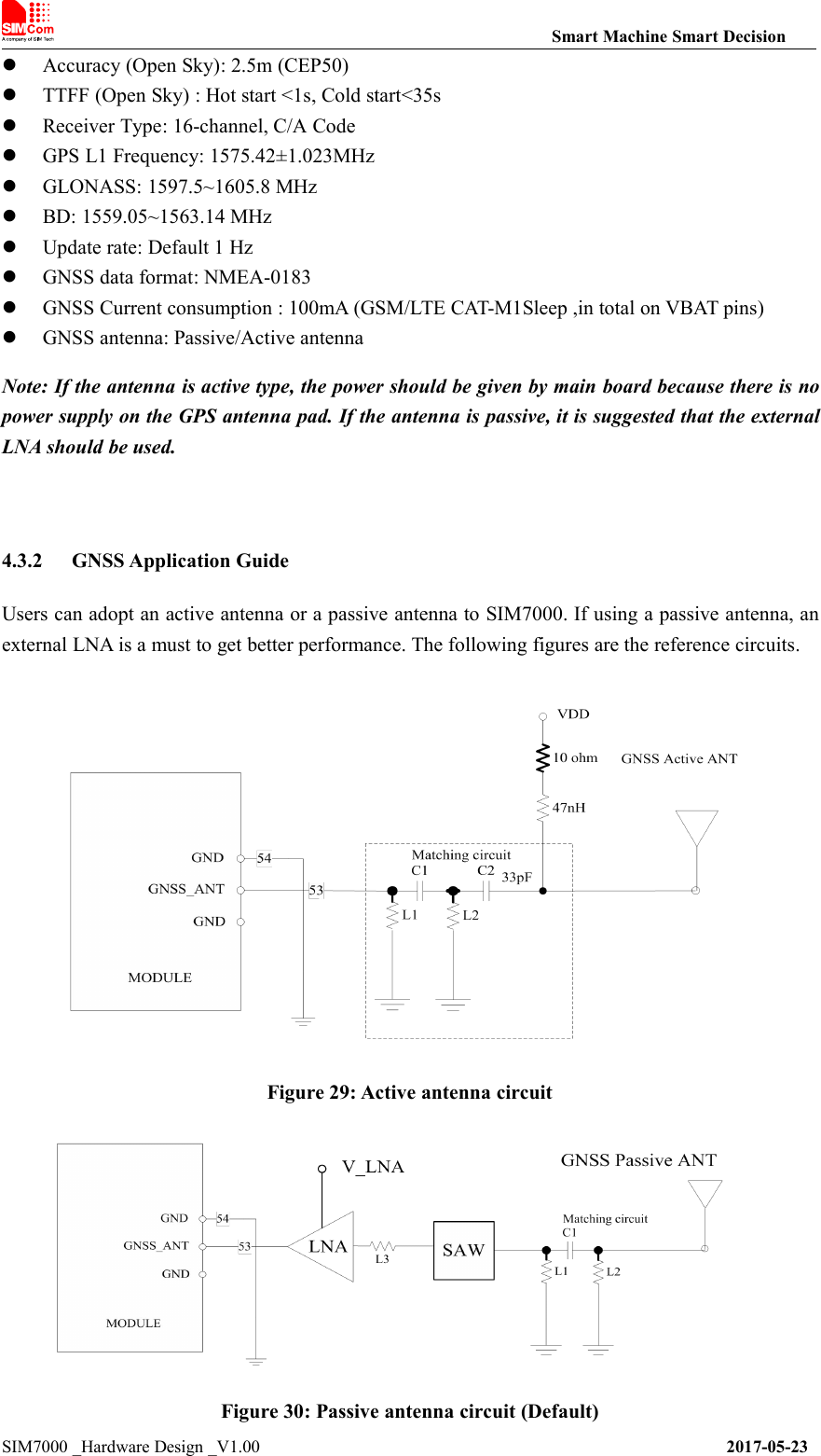
Smart Machine Smart DecisionSIM7000 _Hardware Design _V1.00 2017-05-23Accuracy (Open Sky): 2.5m (CEP50)TTFF (Open Sky) : Hot start <1s, Cold start<35sReceiver Type: 16-channel, C/A CodeGPS L1 Frequency: 1575.42±1.023MHzGLONASS: 1597.5~1605.8 MHzBD: 1559.05~1563.14 MHzUpdate rate: Default 1 HzGNSS data format: NMEA-0183GNSS Current consumption : 100mA (GSM/LTE CAT-M1Sleep ,in total on VBAT pins)GNSS antenna: Passive/Active antennaNote: If the antenna is active type, the power should be given by main board because there is nopower supply on the GPS antenna pad. If the antenna is passive, it is suggested that the externalLNA should be used.4.3.2 GNSS Application GuideUsers can adopt an active antenna or a passive antenna to SIM7000. If using a passive antenna, anexternal LNA is a must to get better performance. The following figures are the reference circuits.Figure 29: Active antenna circuitFigure 30: Passive antenna circuit (Default)
Smart Machine Smart DecisionSIM7000 _Hardware Design _V1.00 2017-05-23In above figures, the components C1, L1 and L2 are used for antenna matching. Usually, the valuesof the components can only be achieved after antenna tuning and usually provided by antennavendor. C2 is used for DC blocking. L3 is the matching component of the external LNA, and thevalue of L3 is determined by the LNA characteristic and PCB layout. Both VDD of active antennaand V_LNA need external power supplies which should be considered according to active antennaand LNA characteristic. LDO/DCDC is recommended to get lower current consuming by shuttingdown active antennas and LNA when GNSS is not working.GNSS can be tested by NMEA port. NMEA sentences can be obtained through UART or USBautomatically. NMEA sentences include GSV, GGA, RMC, GSA, and VTG. Before using GNSS,user should configure SIM7000 in proper operating mode by AT command. Please refer to relateddocuments for details. SIM7000 can also get position location information through AT directly.Note:1. GNSS is closed by default and can be started by “AT+CGNSPWR=1”. The AT command hastwo parameters, the first is on/off, and the second is GNSS mode. Default mode is standalonemode.AGPS mode needs more support from the mobile telecommunication network. Please refer todocument [24] for more details.2. If the passive antenna is used, put the LNA close to the antenna.3. Make sure there are no noise signals around GNSS antenna.
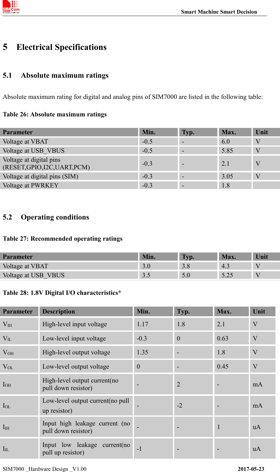
Smart Machine Smart DecisionSIM7000 _Hardware Design _V1.00 2017-05-235Electrical Specifications5.1 Absolute maximum ratingsAbsolute maximum rating for digital and analog pins of SIM7000 are listed in the following table:Table 26: Absolute maximum ratingsParameterMin.Typ.Max.UnitVoltage at VBAT-0.5-6.0VVoltage at USB_VBUS-0.5-5.85VVoltage at digital pins(RESET,GPIO,I2C,UART,PCM)-0.3-2.1VVoltage at digital pins (SIM)-0.3-3.05VVoltage at PWRKEY-0.3-1.85.2 Operating conditionsTable 27: Recommended operating ratingsParameterMin.Typ.Max.UnitVoltage at VBAT3.03.84.3VVoltage at USB_VBUS3.55.05.25VTable 28: 1.8V Digital I/O characteristics*ParameterDescriptionMin.Typ.Max.UnitVIHHigh-level input voltage1.171.82.1VVILLow-level input voltage-0.300.63VVOHHigh-level output voltage1.35-1.8VVOLLow-level output voltage0-0.45VIOHHigh-level output current(nopull down resistor)-2-mAIOLLow-level output current(no pullup resistor)--2-mAIIHInput high leakage current (nopull down resistor)--1uAIILInput low leakage current(nopull up resistor)-1--uA
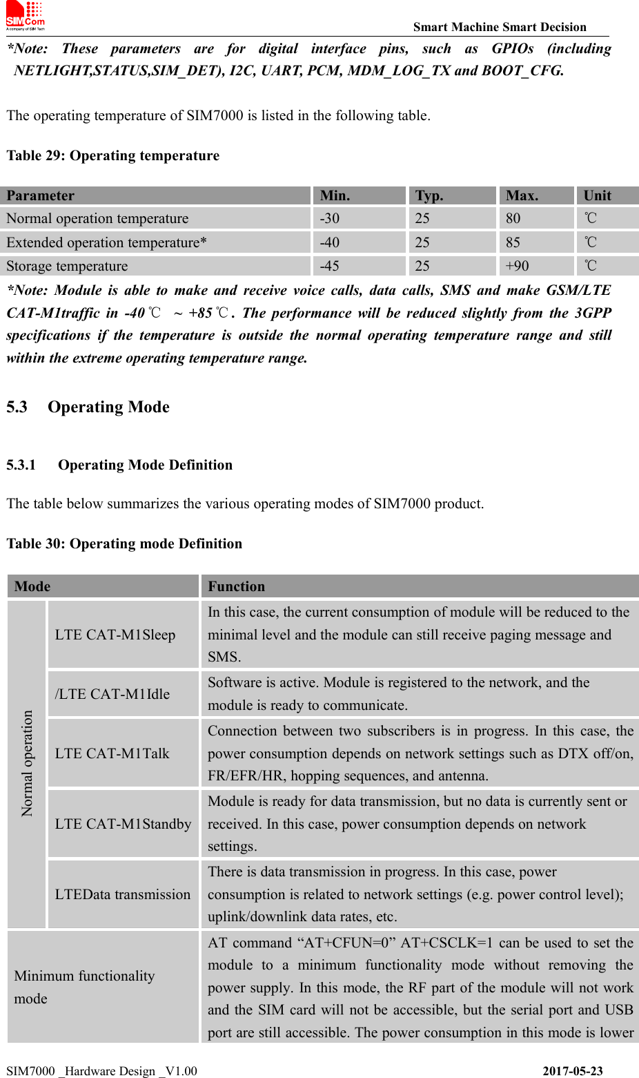
Smart Machine Smart DecisionSIM7000 _Hardware Design _V1.00 2017-05-23*Note: These parameters are for digital interface pins, such as GPIOs (includingNETLIGHT,STATUS,SIM_DET), I2C, UART, PCM, MDM_LOG_TX and BOOT_CFG.The operating temperature of SIM7000 is listed in the following table.Table 29: Operating temperatureParameterMin.Typ.Max.UnitNormal operation temperature-302580℃Extended operation temperature*-402585℃Storage temperature-4525+90℃*Note: Module is able to make and receive voice calls, data calls, SMS and make GSM/LTECAT-M1traffic in -40 ℃~ +85 ℃. The performance will be reduced slightly from the 3GPPspecifications if the temperature is outside the normal operating temperature range and stillwithin the extreme operating temperature range.5.3 Operating Mode5.3.1 Operating Mode DefinitionThe table below summarizes the various operating modes of SIM7000 product.Table 30: Operating mode DefinitionModeFunctionNormal operationLTE CAT-M1SleepIn this case, the current consumption of module will be reduced to theminimal level and the module can still receive paging message andSMS./LTE CAT-M1IdleSoftware is active. Module is registered to the network, and themodule is ready to communicate.LTE CAT-M1TalkConnection between two subscribers is in progress. In this case, thepower consumption depends on network settings such as DTX off/on,FR/EFR/HR, hopping sequences, and antenna.LTE CAT-M1StandbyModule is ready for data transmission, but no data is currently sent orreceived. In this case, power consumption depends on networksettings.LTEData transmissionThere is data transmission in progress. In this case, powerconsumption is related to network settings (e.g. power control level);uplink/downlink data rates, etc.Minimum functionalitymodeAT command “AT+CFUN=0” AT+CSCLK=1 can be used to set themodule to a minimum functionality mode without removing thepower supply. In this mode, the RF part of the module will not workand the SIM card will not be accessible, but the serial port and USBport are still accessible. The power consumption in this mode is lower
Smart Machine Smart DecisionSIM7000 _Hardware Design _V1.00 2017-05-23than normal mode.Flight modeAT command “AT+CFUN=4” can be used to set the module to flightmode without removing the power supply. In this mode, the RF partof the module will not work, but the serial port and USB port are stillaccessible. The power consumption in this mode is lower than normalmode.PSM modeSetting the timer of the software can be entered PSM mode. In thismode, the module will be the least current consumption. Meanwhile,all the output of the LDO and DCDC in the module will be closedexcept the RTC power. And also all of the functions will beunavailable except the RTC function. RTC timer can wake up themodule.Power off modeModule will go into power off mode by sending the AT command“AT+CPOWD” or pull down the PWRKEY pin, normally. In thismode the power management unit shuts down the power supply, andsoftware is not active. The serial port and USB are is not accessible.5.3.2 Sleep modeIn sleep mode, the current consumption of module will be reduced to the minimal level, andmodule can still receive paging message and SMS.Several hardware and software conditions must be satisfied together in order to let SIM7000 entersleep mode:1. UART condition2. USB condition3. Software conditionNote: Before designing, pay attention to how to realize sleeping/waking function and refer toDocument [26] for more details.5.3.3 Minimum functionality mode and Flight modeMinimum functionality mode ceases a majority function of the module, thus minimizing the powerconsumption. This mode is set by the AT command which provides a choice of the functionalitylevels.●AT+CFUN=0: Minimum functionality●AT+CFUN=1: Full functionality (Default)●AT+CFUN=4: Flight modeIf SIM7000 has been set to minimum functionality mode, the RF function and SIM card functionwill be closed. In this case, the serial port and USB are still accessible, but RF function and SIMcard will be unavailable.If SIM7000 has been set to flight mode, the RF function will be closed. In this case, the serial portand USB are still accessible, but RF function will be unavailable.
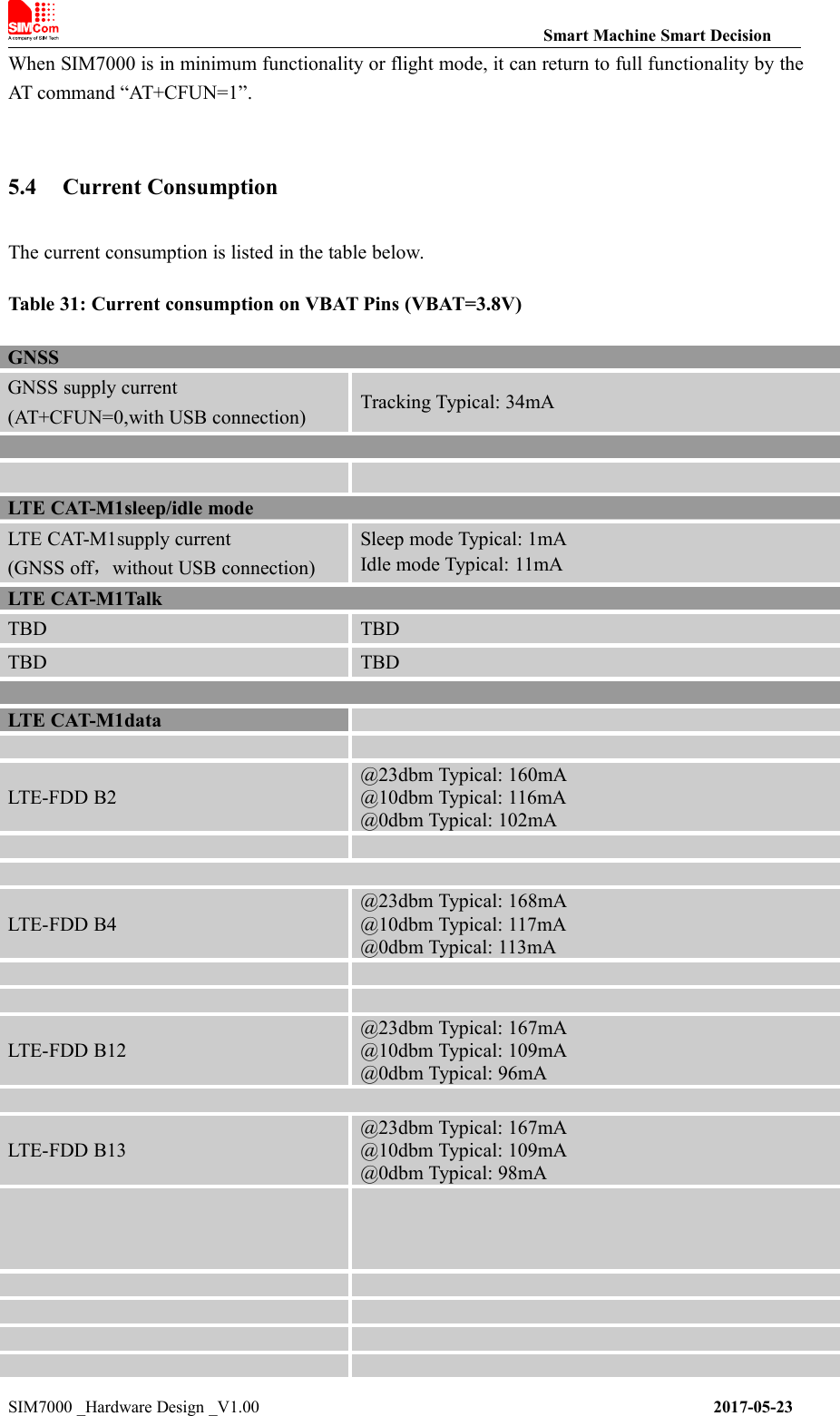
Smart Machine Smart DecisionSIM7000 _Hardware Design _V1.00 2017-05-23When SIM7000 is in minimum functionality or flight mode, it can return to full functionality by theAT command “AT+CFUN=1”.5.4 Current ConsumptionThe current consumption is listed in the table below.Table 31: Current consumption on VBAT Pins (VBAT=3.8V)GNSSGNSS supply current(AT+CFUN=0,with USB connection)Tracking Typical: 34mALTE CAT-M1sleep/idle modeLTE CAT-M1supply current(GNSS off,without USB connection)Sleep mode Typical: 1mAIdle mode Typical: 11mALTE CAT-M1TalkTBDTBDTBDTBDLTE CAT-M1dataLTE-FDD B2@23dbm Typical: 160mA@10dbm Typical: 116mA@0dbm Typical: 102mALTE-FDD B4@23dbm Typical: 168mA@10dbm Typical: 117mA@0dbm Typical: 113mALTE-FDD B12@23dbm Typical: 167mA@10dbm Typical: 109mA@0dbm Typical: 96mALTE-FDD B13@23dbm Typical: 167mA@10dbm Typical: 109mA@0dbm Typical: 98mA
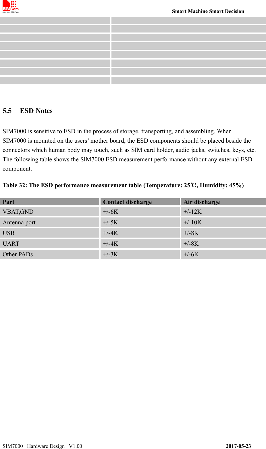
Smart Machine Smart DecisionSIM7000 _Hardware Design _V1.00 2017-05-235.5 ESD NotesSIM7000 is sensitive to ESD in the process of storage, transporting, and assembling. WhenSIM7000 is mounted on the users’ mother board, the ESD components should be placed beside theconnectors which human body may touch, such as SIM card holder, audio jacks, switches, keys, etc.The following table shows the SIM7000 ESD measurement performance without any external ESDcomponent.Table 32: The ESD performance measurement table (Temperature: 25℃, Humidity: 45%)PartContact dischargeAir dischargeVBAT,GND+/-6K+/-12KAntenna port+/-5K+/-10KUSB+/-4K+/-8KUART+/-4K+/-8KOther PADs+/-3K+/-6K
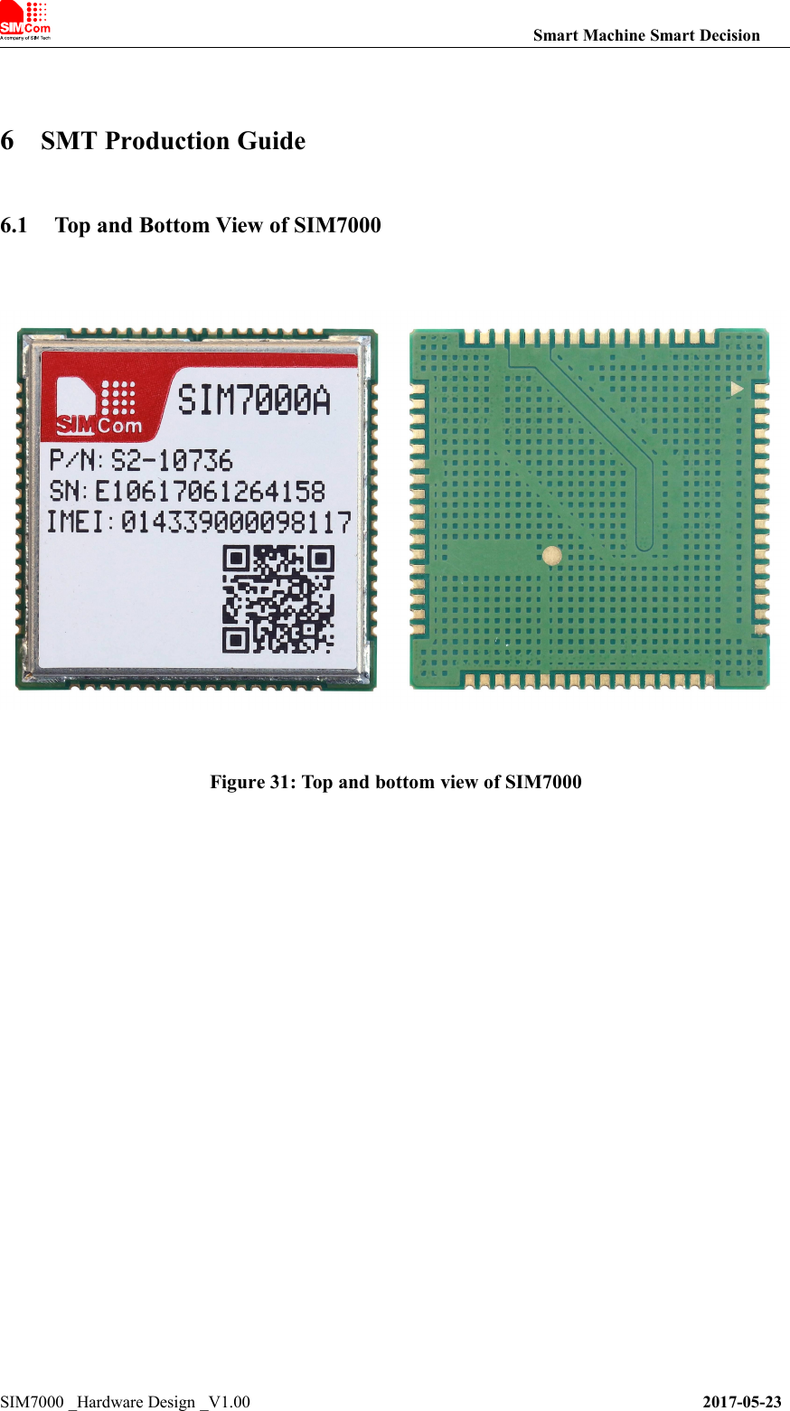
Smart Machine Smart DecisionSIM7000 _Hardware Design _V1.00 2017-05-236SMT Production Guide6.1 Top and Bottom View of SIM7000Figure 31: Top and bottom view of SIM7000
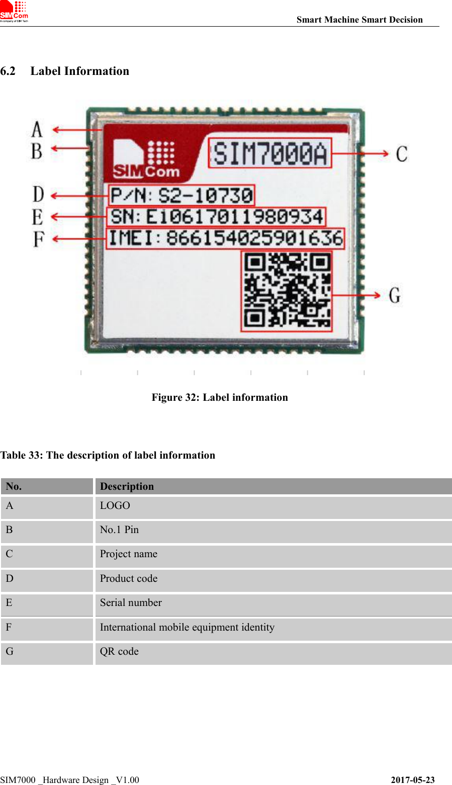
Smart Machine Smart DecisionSIM7000 _Hardware Design _V1.00 2017-05-236.2 Label InformationFigure 32: Label informationTable 33: The description of label informationNo.DescriptionALOGOBNo.1 PinCProject nameDProduct codeESerial numberFInternational mobile equipment identityGQR code
Smart Machine Smart DecisionSIM7000 _Hardware Design _V1.00 2017-05-236.3 Typical SMT Reflow ProfileSIMCom provides a typical soldering profile. Therefore the soldering profile shown below is onlya generic recommendation and should be adjusted to the specific application and manufacturingconstraints.Figure 33: The ramp-soak-spike reflow profile of SIM7000Note: For more details about secondary SMT, please refer to the document [21].6.4 Moisture Sensitivity Level (MSL)SIM7000 is qualified to Moisture Sensitivity Level (MSL) 3 in accordance with JEDEC J-STD-033.If the prescribed time limit is exceeded, users should bake modules for 192 hours in dryingequipment (<5% RH) at 40+5/-0°C, or 72 hours at 85+5/-5°C. Note that plastic tray is notheat-resistant, and only can be baked at 45° C.Table 34: Moisture Sensitivity Level and Floor LifeMoisture Sensitivity Level(MSL)Floor Life (out of bag) at factory ambient≤30°C/60% RH or asstated1Unlimited at ≦30℃/85% RH21 year2a4 weeks3168 hours472 hours548 hours5a24 hours6Mandatory bake before use. After bake, it must be reflowed within the
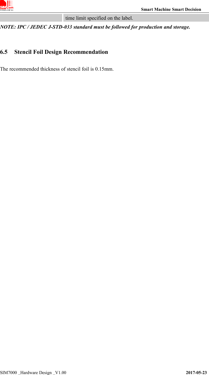
Smart Machine Smart DecisionSIM7000 _Hardware Design _V1.00 2017-05-23time limit specified on the label.NOTE: IPC / JEDEC J-STD-033 standard must be followed for production and storage.6.5 Stencil Foil Design RecommendationThe recommended thickness of stencil foil is 0.15mm.
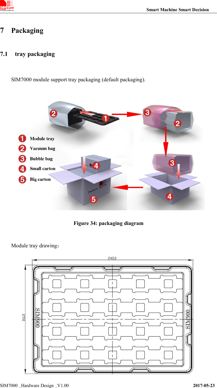
Smart Machine Smart DecisionSIM7000 _Hardware Design _V1.00 2017-05-237Packaging7.1 tray packagingSIM7000 module support tray packaging (default packaging).Figure 34: packaging diagramModule tray drawing:
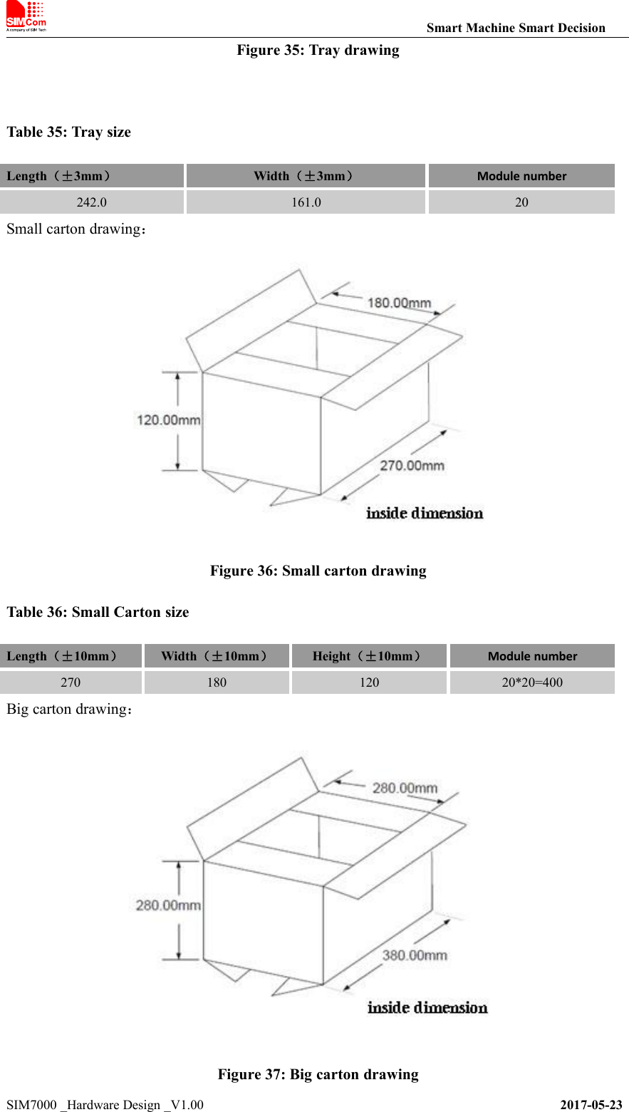
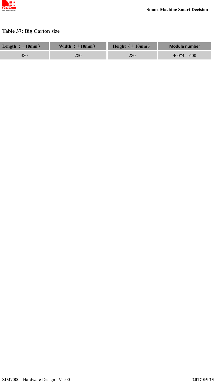
Smart Machine Smart DecisionSIM7000 _Hardware Design _V1.00 2017-05-23Figure 35: Tray drawingTable 35: Tray sizeLength(±3mm)Width(±3mm)Module number242.0161.020Small carton drawing:Figure 36: Small carton drawingTable 36: Small Carton sizeLength(±10mm)Width(±10mm)Height(±10mm)Module number27018012020*20=400Big carton drawing:Figure 37: Big carton drawing
Smart Machine Smart DecisionSIM7000 _Hardware Design _V1.00 2017-05-23Table 37: Big Carton sizeLength(±10mm)Width(±10mm)Height(±10mm)Module number380280280400*4=1600
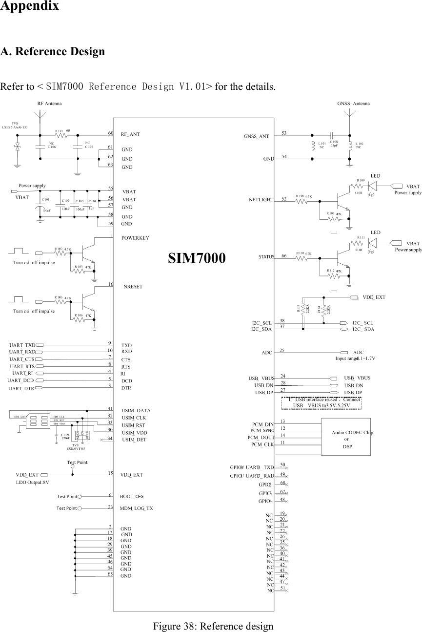
AppendixA. Reference DesignRefer to < SIM7000 Reference Design V1.01> for the details.Figure 38: Reference design
Smart Machine Smart DecisionSIM7000 _Hardware Design _V1.00 2017-05-23B. Related DocumentsTable 38: Related DocumentsNO.TitleDescription[1]SIM7X00 Series_ATCommand Manual_V1.xxAT Command Manual[2]ITU-T Draft newrecommendationV.25terSerial asynchronous automatic dialing and control[3]GSM 07.07Digital cellular telecommunications (Phase 2+); AT commandset for GSM Mobile Equipment (ME)[4]GSM 07.10Support GSM 07.10 multiplexing protocol[5]GSM 07.05Digital cellular telecommunications (Phase 2+); Use of DataTerminal Equipment – Data Circuit terminating Equipment(DTE – DCE) interface for Short Message Service (SMS)and Cell Broadcast Service (CBS)[6]GSM 11.14Digital cellular telecommunications system (Phase 2+);Specification of the SIM Application Toolkit for theSubscriber Identity Module – Mobile Equipment (SIM – ME)interface[7]GSM 11.11Digital cellular telecommunications system (Phase 2+);Specification of the Subscriber Identity Module – MobileEquipment (SIM – ME) interface[8]GSM 03.38Digital cellular telecommunications system (Phase 2+);Alphabets and language-specific information[9]GSM 11.10Digital cellular telecommunications system (Phase 2) ;Mobile Station (MS) conformance specification ;Part 1:Conformance specification[10]3GPP TS 51.010-1Digital cellular telecommunications system (Release 5);Mobile Station (MS) conformance specification[11]3GPP TS 34.124Electromagnetic Compatibility (EMC) for mobile terminalsand ancillary equipment.[12]3GPP TS 34.121Electromagnetic Compatibility (EMC) for mobile terminalsand ancillary equipment.[13]3GPP TS 34.123-1Technical Specification Group Radio Access Network;Terminal conformance specification; Radio transmission andreception (FDD)[14]3GPP TS 34.123-3User Equipment (UE) conformance specification; Part 3:Abstract Test Suites.[15]EN 301 908-02 V2.2.1Electromagnetic compatibility and Radio spectrum Matters(ERM); Base Stations (BS) and User Equipment (UE) forIMT-2000. Third Generation cellular networks; Part 2:Harmonized EN for IMT-2000, CDMA Direct Spread(UTRA FDD) (UE) covering essential requirements of article3.2 of the R&TTE Directive[16]EN 301 489-24 V1.2.1Electromagnetic compatibility and Radio Spectrum Matters(ERM); Electromagnetic Compatibility (EMC) standard forradio equipment and services; Part 24: Specific conditions forIMT-2000 CDMA Direct Spread (UTRA) for Mobile andportable (UE) radio and ancillary equipment[17]IEC/EN60950-1(2001)Safety of information technology equipment (2000)
Smart Machine Smart DecisionSIM7000 _Hardware Design _V1.00 2017-05-23[18]3GPP TS 51.010-1Digital cellular telecommunications system (Release 5);Mobile Station (MS) conformance specification[19]GCF-CC V3.23.1Global Certification Forum - Certification Criteria[20]2002/95/ECDirective of the European Parliament and of the Council of27 January 2003 on the restriction of the use of certainhazardous substances in electrical and electronic equipment(RoHS)[21]Modulesecondary-SMT-UGD-V1.xxModule secondary SMT Guidelines[22]SIM7X00Series_UART_ApplicationNote_V1.xxThis document describes how to use UART interface ofSIMCom modules.[23]SIM7X00 Series_USBAUDIO_ApplicationNote_V1.xxUSB AUDIO Application Note[24]SIM7X00Series_GPS_ApplicationNote_V1.xxGPS Application Note[25]Antenna design guidelines fordiversity receiver systemAntenna design guidelines for diversity receiver system[26]SIM7X00 Series_Sleep Mode_Application Note_V1.xxSleep Mode Application Note
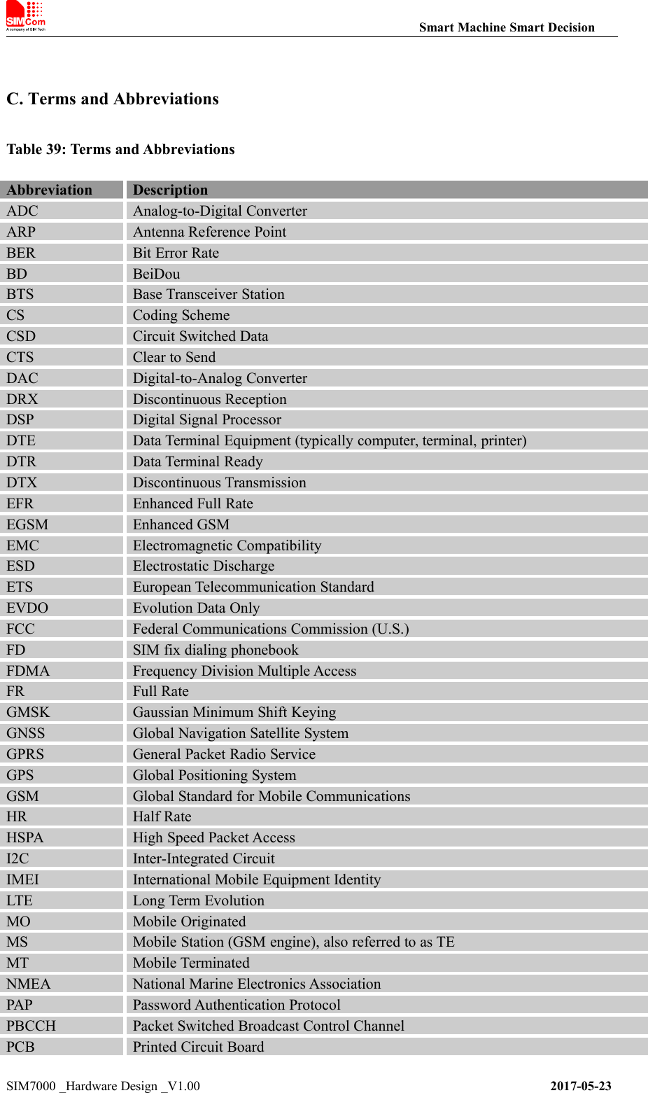
Smart Machine Smart DecisionSIM7000 _Hardware Design _V1.00 2017-05-23C. Terms and AbbreviationsTable 39: Terms and AbbreviationsAbbreviationDescriptionADCAnalog-to-Digital ConverterARPAntenna Reference PointBERBit Error RateBDBeiDouBTSBase Transceiver StationCSCoding SchemeCSDCircuit Switched DataCTSClear to SendDACDigital-to-Analog ConverterDRXDiscontinuous ReceptionDSPDigital Signal ProcessorDTEData Terminal Equipment (typically computer, terminal, printer)DTRData Terminal ReadyDTXDiscontinuous TransmissionEFREnhanced Full RateEGSMEnhanced GSMEMCElectromagnetic CompatibilityESDElectrostatic DischargeETSEuropean Telecommunication StandardEVDOEvolution Data OnlyFCCFederal Communications Commission (U.S.)FDSIM fix dialing phonebookFDMAFrequency Division Multiple AccessFRFull RateGMSKGaussian Minimum Shift KeyingGNSSGlobal Navigation Satellite SystemGPRSGeneral Packet Radio ServiceGPSGlobal Positioning SystemGSMGlobal Standard for Mobile CommunicationsHRHalf RateHSPAHigh Speed Packet AccessI2CInter-Integrated CircuitIMEIInternational Mobile Equipment IdentityLTELong Term EvolutionMOMobile OriginatedMSMobile Station (GSM engine), also referred to as TEMTMobile TerminatedNMEANational Marine Electronics AssociationPAPPassword Authentication ProtocolPBCCHPacket Switched Broadcast Control ChannelPCBPrinted Circuit Board
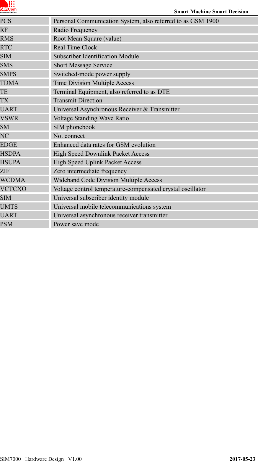
Smart Machine Smart DecisionSIM7000 _Hardware Design _V1.00 2017-05-23PCSPersonal Communication System, also referred to as GSM 1900RFRadio FrequencyRMSRoot Mean Square (value)RTCReal Time ClockSIMSubscriber Identification ModuleSMSShort Message ServiceSMPSSwitched-mode power supplyTDMATime Division Multiple AccessTETerminal Equipment, also referred to as DTETXTransmit DirectionUARTUniversal Asynchronous Receiver & TransmitterVSWRVoltage Standing Wave RatioSMSIM phonebookNCNot connectEDGEEnhanced data rates for GSM evolutionHSDPAHigh Speed Downlink Packet AccessHSUPAHigh Speed Uplink Packet AccessZIFZero intermediate frequencyWCDMAWideband Code Division Multiple AccessVCTCXOVoltage control temperature-compensated crystal oscillatorSIMUniversal subscriber identity moduleUMTSUniversal mobile telecommunications systemUARTUniversal asynchronous receiver transmitterPSMPower save mode
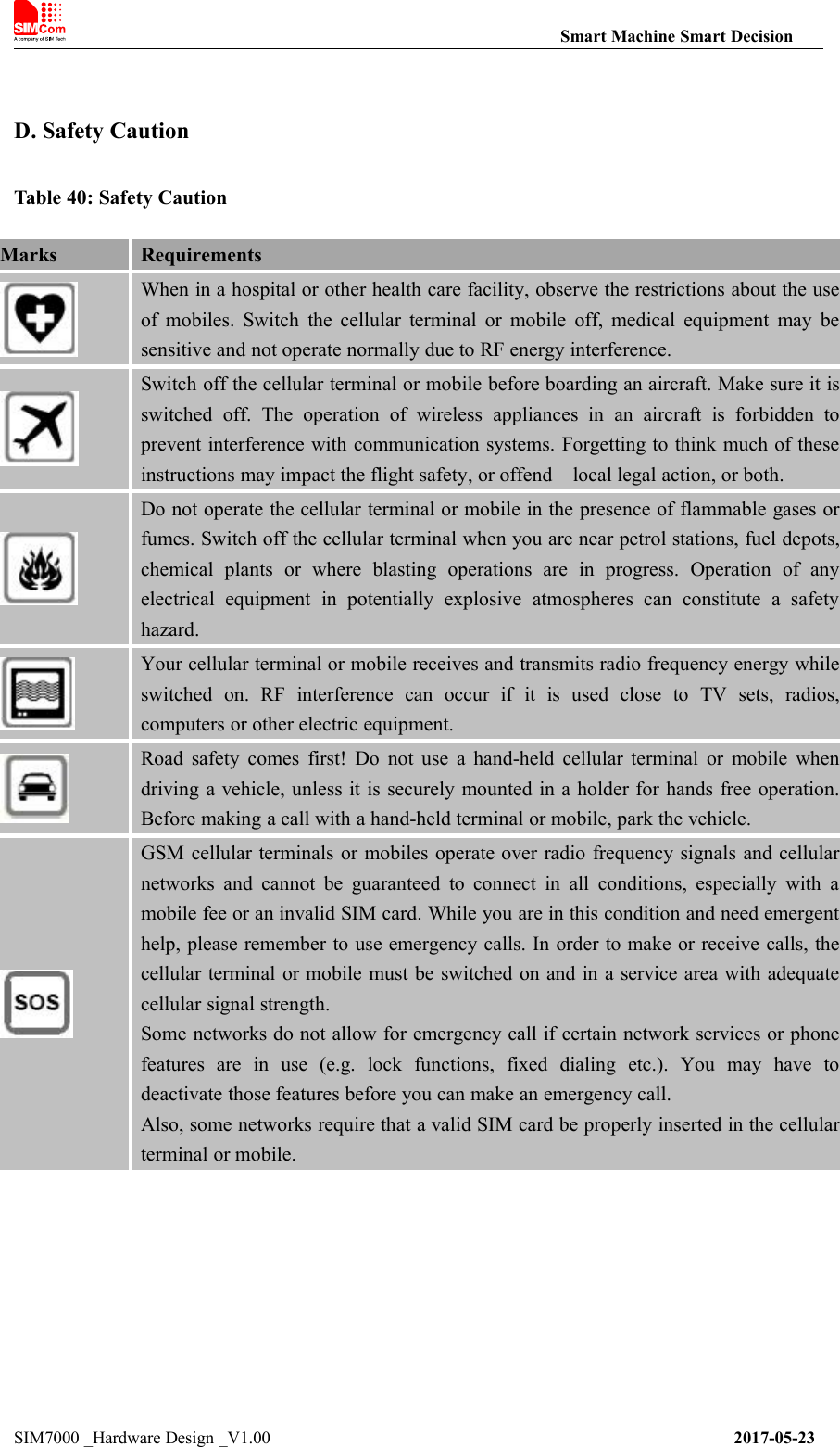
Smart Machine Smart DecisionSIM7000 _Hardware Design _V1.00 2017-05-23D. Safety CautionTable 40: Safety CautionMarksRequirementsWhen in a hospital or other health care facility, observe the restrictions about the useof mobiles. Switch the cellular terminal or mobile off, medical equipment may besensitive and not operate normally due to RF energy interference.Switch off the cellular terminal or mobile before boarding an aircraft. Make sure it isswitched off. The operation of wireless appliances in an aircraft is forbidden toprevent interference with communication systems. Forgetting to think much of theseinstructions may impact the flight safety, or offend local legal action, or both.Do not operate the cellular terminal or mobile in the presence of flammable gases orfumes. Switch off the cellular terminal when you are near petrol stations, fuel depots,chemical plants or where blasting operations are in progress. Operation of anyelectrical equipment in potentially explosive atmospheres can constitute a safetyhazard.Your cellular terminal or mobile receives and transmits radio frequency energy whileswitched on. RF interference can occur if it is used close to TV sets, radios,computers or other electric equipment.Road safety comes first! Do not use a hand-held cellular terminal or mobile whendriving a vehicle, unless it is securely mounted in a holder for hands free operation.Before making a call with a hand-held terminal or mobile, park the vehicle.GSM cellular terminals or mobiles operate over radio frequency signals and cellularnetworks and cannot be guaranteed to connect in all conditions, especially with amobile fee or an invalid SIM card. While you are in this condition and need emergenthelp, please remember to use emergency calls. In order to make or receive calls, thecellular terminal or mobile must be switched on and in a service area with adequatecellular signal strength.Some networks do not allow for emergency call if certain network services or phonefeatures are in use (e.g. lock functions, fixed dialing etc.). You may have todeactivate those features before you can make an emergency call.Also, some networks require that a valid SIM card be properly inserted in the cellularterminal or mobile.
Smart Machine Smart DecisionSIM7000 _Hardware Design _V1.00 2017-05-23Contact us:Shanghai SIMCom Wireless Solutions Ltd.Add: SIM Technology Building, No.633, Jinzhong Road, Changning District, Shanghai P.R. China200335Tel:+86 21 3235 3300Fax:+86 21 3235 3020URL:www.simcomm2m.com

Navigation menu