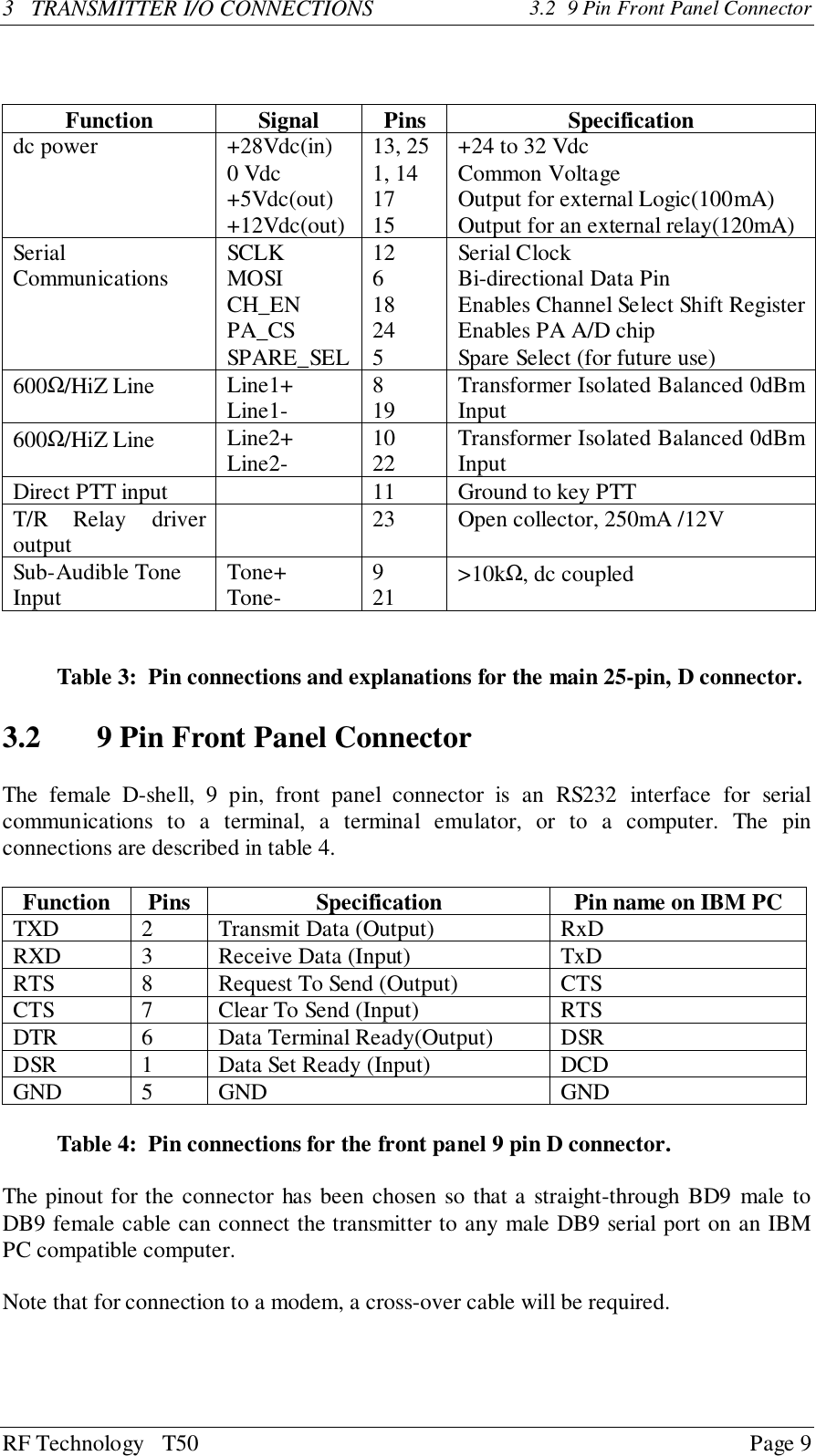
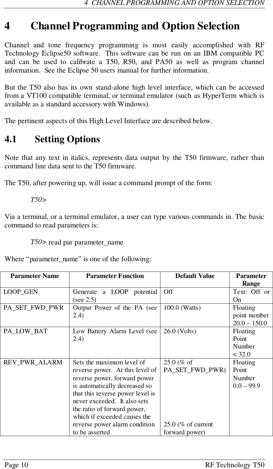
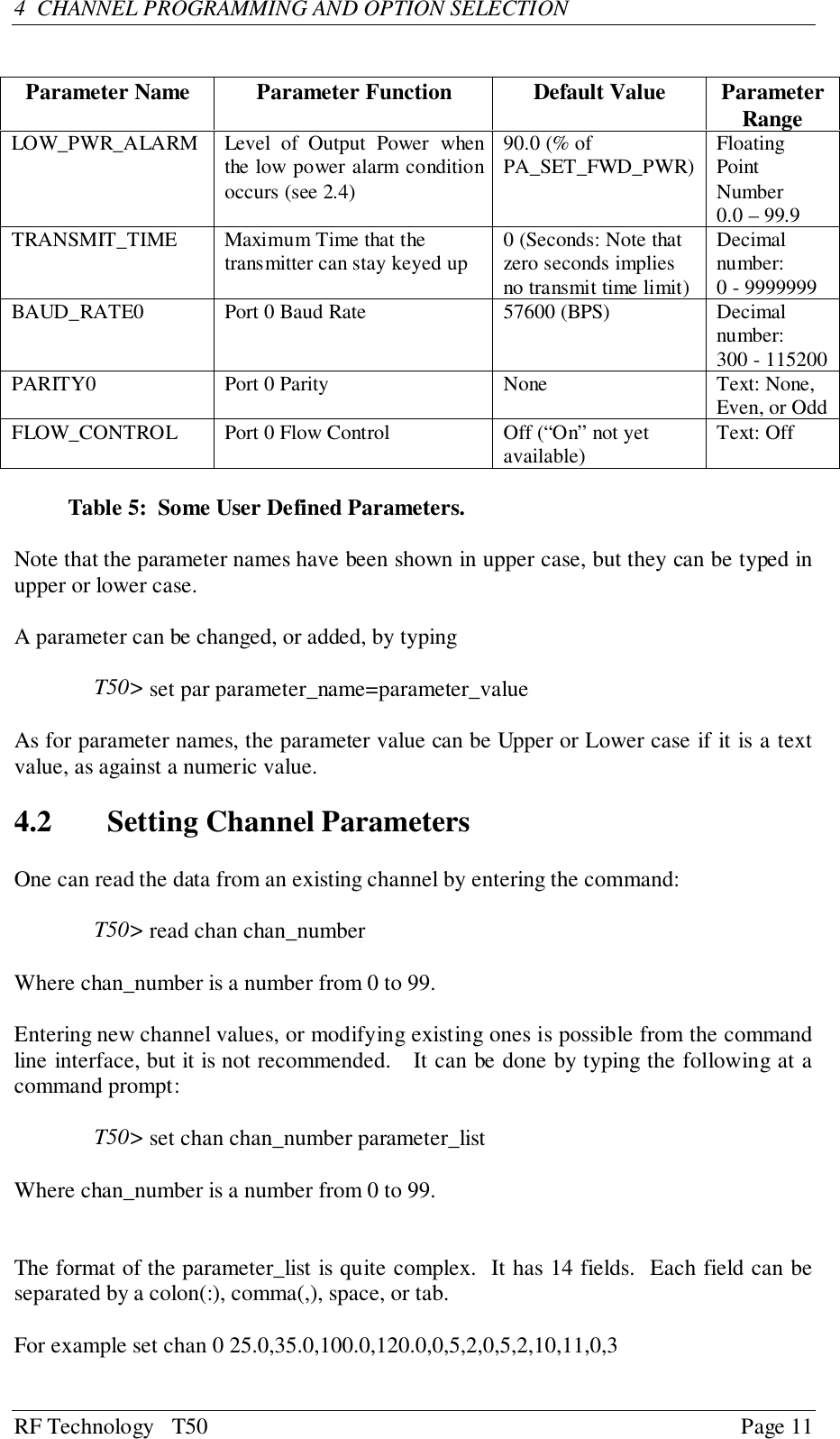
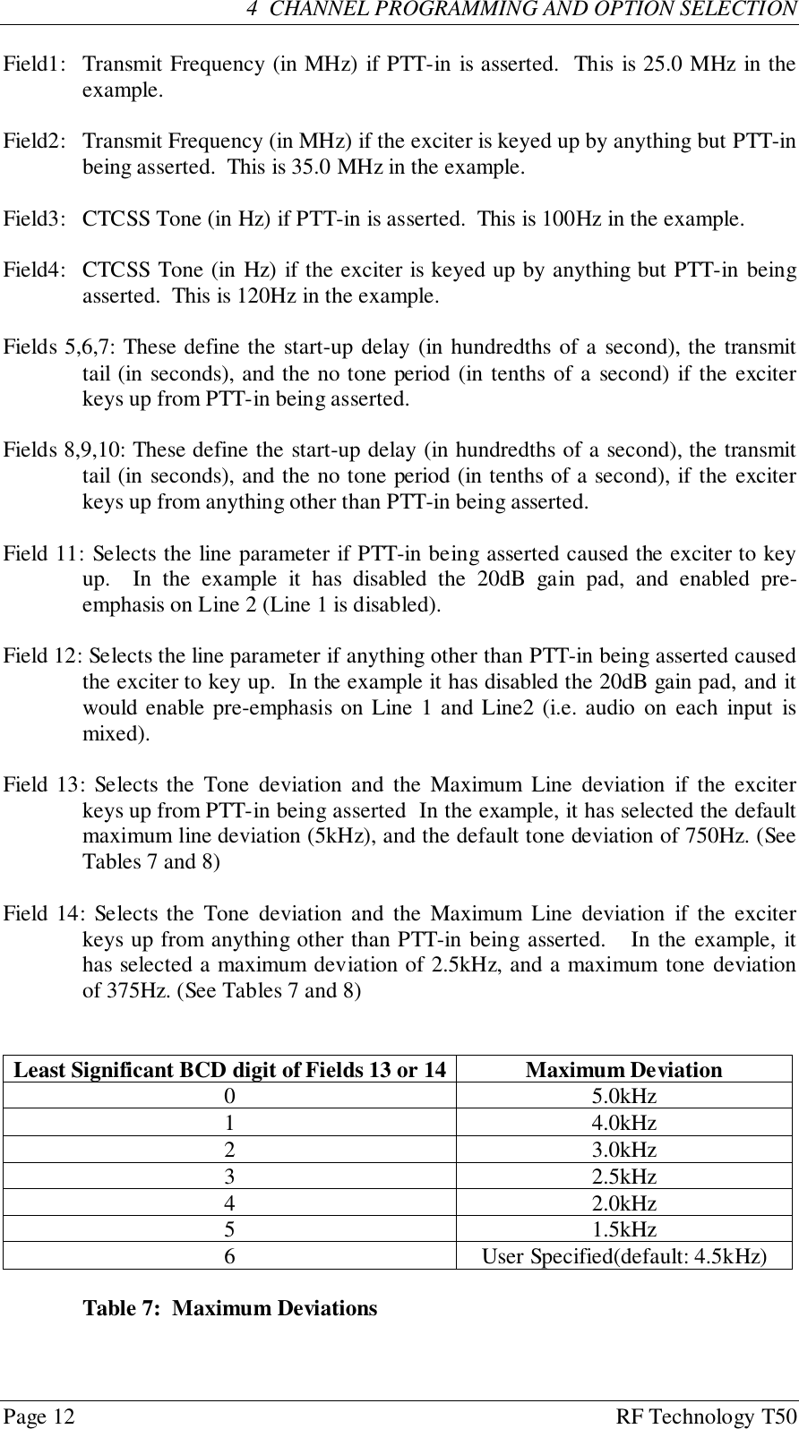
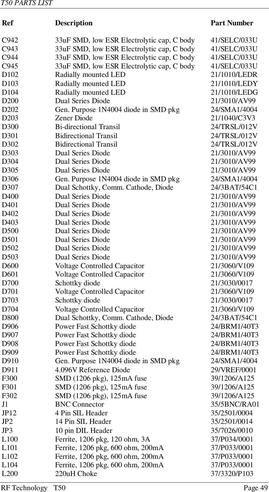
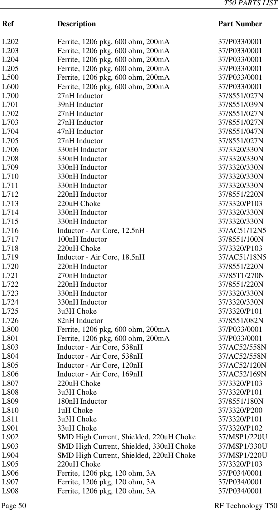
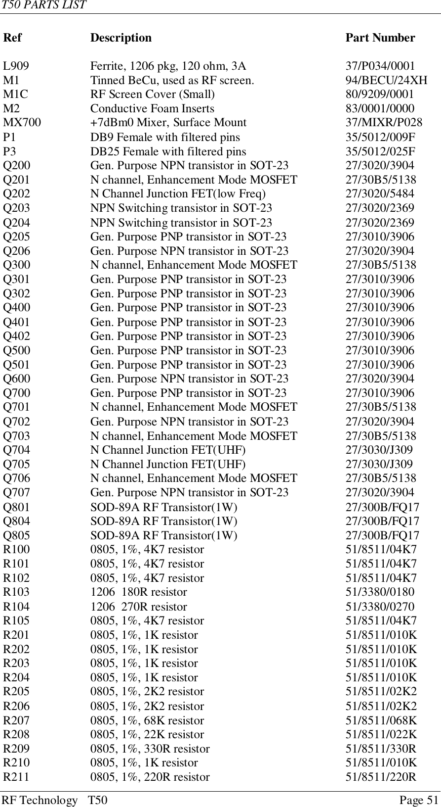
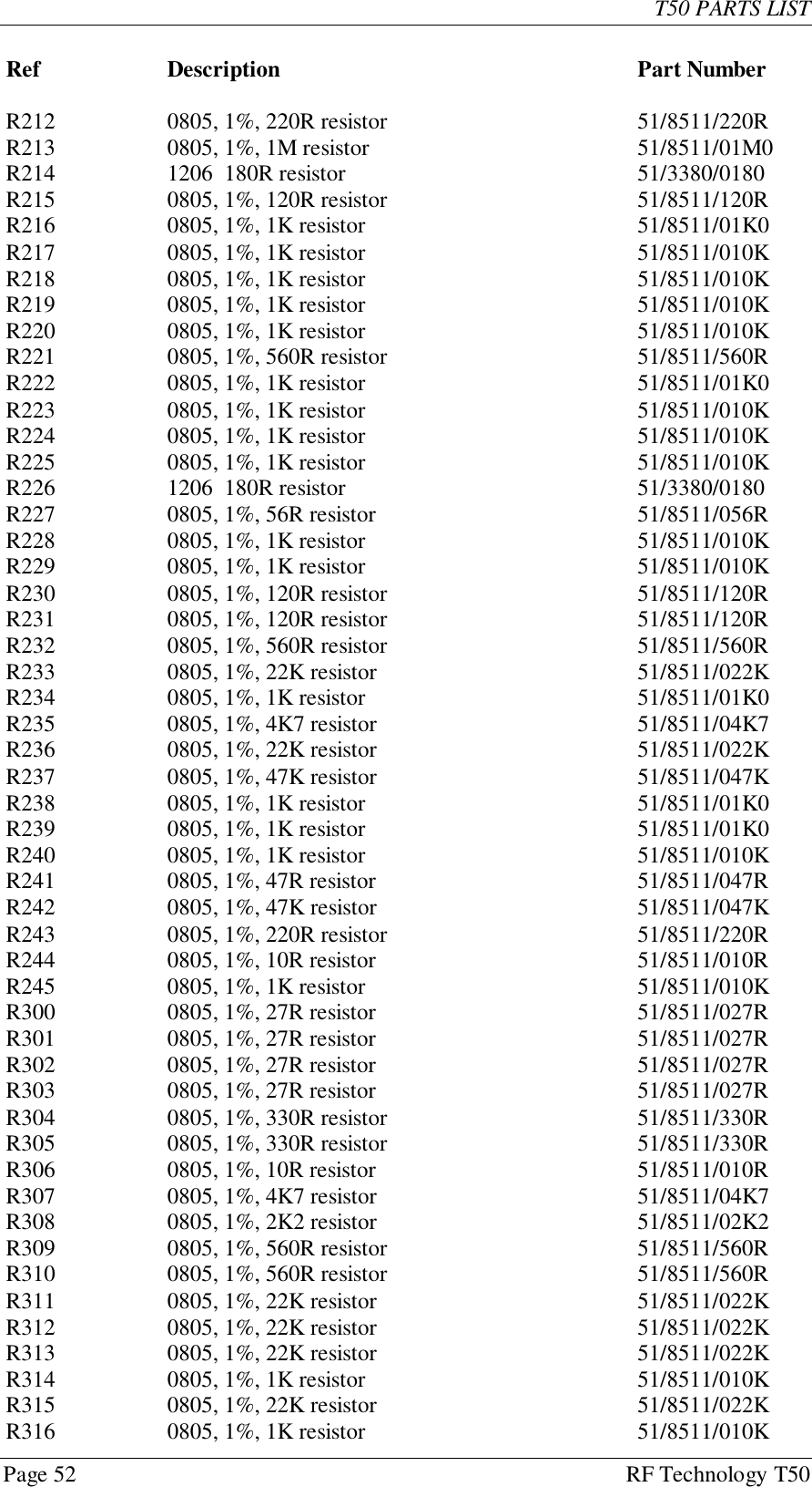
RF Technology 50A 25 - 50 MHz Base Station Transceiver User Manual Exciter operations manual
RF Technology Pty Ltd 25 - 50 MHz Base Station Transceiver Exciter operations manual
Contents
- 1. Receiver operations manual
- 2. Power amplifier operations manual
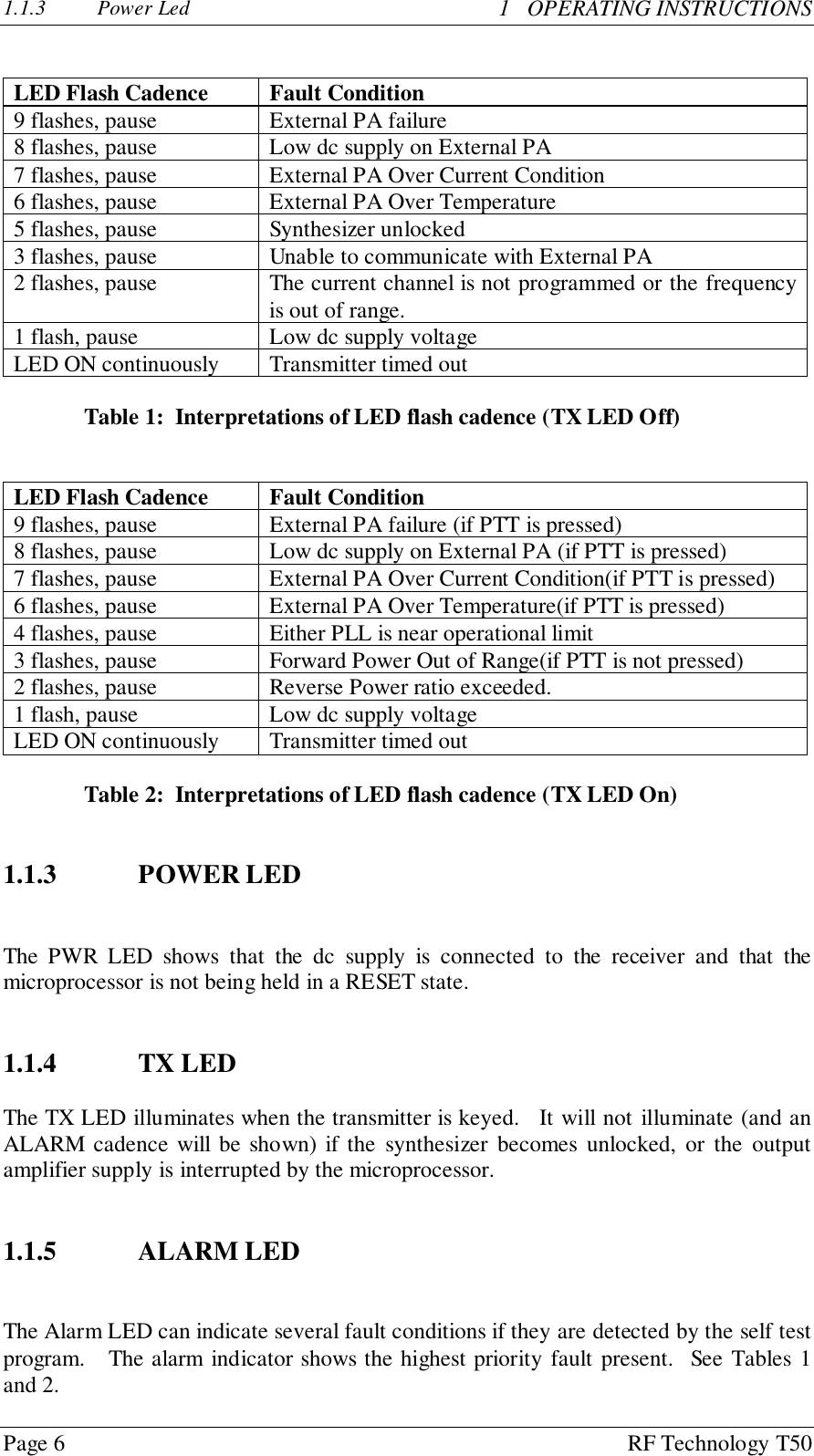
- 3. Exciter operations manual
Exciter operations manual