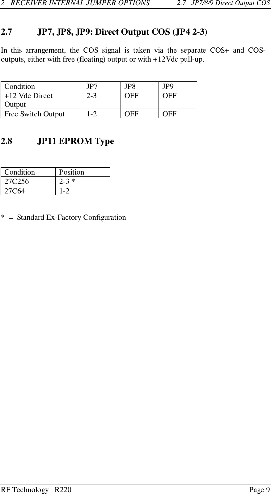
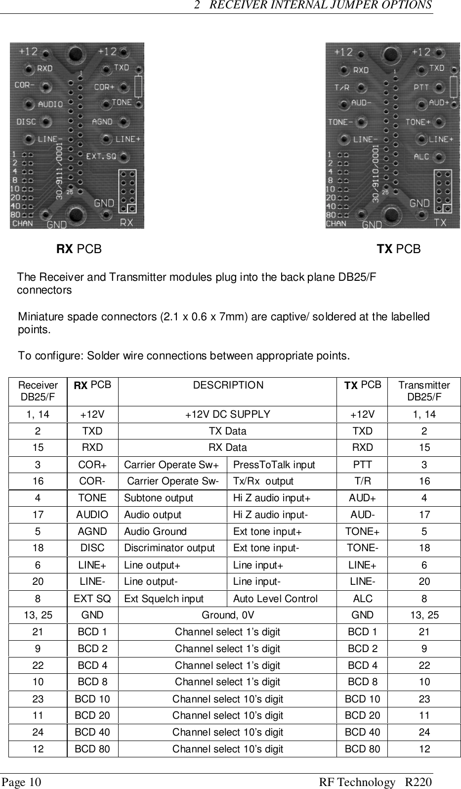
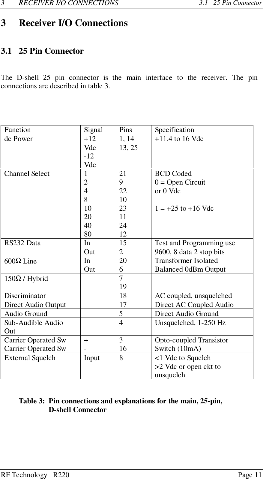
RF Technology 200A-AN Base station User Manual Receiver manual

RF Technology Pty Ltd Base station Receiver manual

Contents

  • 1. Receiver manual
  • 2.

Receiver manual

Eclipse SeriesRF Technologyrfinfo@rftechnology.com.auNovember 2001R220 ReceiverOperation and Maintenance ManualThis manual is produced by RF Technology Pty Ltd.,10/8 Leighton Place, Hornsby, 2077, Australia, and isCopyright ©2001, RF TechnologyPart No. PCB 30/9132
Page 2 RF Technology   R220CONTENTS CONTENTSContents1 Operating Instructions 51.1 Front Panel Controls and Indicators 51.1.1 Mon. Volume 51.1.2 Mon. Sq. 51.1.3 N. SQ 51.1.4 C. SQ 61.1.5 Line 61.1.6 PWR LED 61.1.7 SQ LED 61.1.8 Alarm LED 72 Receiver Internal Jumper Options 72.1 JP1:   240Hz Notch Filter 72.2 JP2:   Audio Response 82.3 JP3:   Audio Filter In/Out 82.4 JP4:   600Ω Line dc Loop COS 82.5 JP6:   COS Polarity 82.6 JP7/8/9:   dc Loop COS Configuration 82.7 JP7, JP8, JP9:   Direct Output COS 92.8 JP11 EPROM Type 93 Receiver I/O Connections 113.1 25 Pin Connector 114 Channel and Tone Frequency Programming 125 Circuit Description 125.1 RF Section 125.2 IF Section 125.3 VCO Section 135.4 PLL Section  135.5 Audio Signal Processing 145.6 Noise Filter, Amplifier and Detector 145.7 Subtone Filter and CTCSS 145.8 External Squelch 155.9 Microprocessor Controller 155.10 Carrier Operated Switch 155.11 Voltage Regulator 166 Alignment Procedure 166.1 Standard Input Signal 166.2 RF Alignment 166.3 IF Alignment 176.4 Line Level Adjustment 186.5 Reference Oscillator Calibration 18
RF Technology   R220 Page 3CONTENTS CONTENTS7 Specifications 187.1 General Description 187.1.1 Channel Capacity 187.1.2 CTCSS 187.1.3 Channel Programming 187.1.4 Channel Selection 197.1.5 Microprocessor 197.2 Physical Configuration 197.3 Front Panel Controls, Indicators and Test Points 197.3.1 Controls 197.3.2 Indicators 197.3.3 Test Points 207.4 Electrical Specifications 207.4.1 Power Requirements 207.4.2 Frequency Range and Channel Spacing 207.4.3 Frequency Synthesizer Step Size 207.4.4 Frequency Stability 207.4.5 Nominal Antenna Impedance 207.4.6 IF Frequencies 217.4.7 Sensitivity 217.4.8 Selectivity 217.4.9 Spurious and Image Rejection 217.4.10 Intermodulation 217.4.11 Modulation Acceptance BW 217.4.12 Noise Squelch 217.4.13 Carrier Level Squelch 227.4.14 Receiver Frequency Spread 227.4.15 Receiver Conducted Spurious Emissions 227.4.16 Audio Frequency Response 227.4.17 Audio Output Level 227.4.18 Audio Distortion 227.4.19 Channel Select Input/Output 227.4.20 Carrier Operated Switch Output 237.4.21 CTCSS 237.4.22 External Squelch Input 257.5 Connectors 257.5.1 Antenna Connector 257.5.2 Power and I/O Connector 257.5.3 Test Connector 25
Page 4 RF Technology   R220CONTENTS CONTENTSBParts List
RF Technology   R220 Page 51 OPERATING INSTRUCTIONSWARNINGChanges or modifications not expressly approvedby RF Technology could void your authority tooperate this equipment.  Specifications may varyfrom those given in this document in accordancewith requirements of local authorities. RFTechnology equipment is subject to continualimprovement and RF Technology reserves the rightto change performance and specification withoutfurther notice.1 Operating Instructions1.1 Front Panel Controls and Indicators1.1.1 Mon. VolumeThe Mon. Volume control is used to adjust the volume of the internal loudspeakerand any external speaker connected to the test socket. It does not effect the level ofthe 600Ω line or direct audio output.1.1.2 Mon. SQ.The Mon. SQ. switch allows all squelch functions controlling the monitor output tobe disabled. When the switch is in the Mon. SQ. position the audio at the monitorspeaker is controlled by the noise detector.  The CTCSS, carrier and external squelchfunctions are disabled.  This can be useful when you are trying to trace the source ofon-channel interference or when setting the noise squelch threshold.  the audio fromthe 600Ω line and direct outputs is not effected by the switch position.1.1.3 N.SQThe N.SQ trimpot is used to set the noise squelch sensitivity.   Use the followingprocedure to set the noise squelch to maximum sensitivity.1. Set the toggle switch to the Mon. Sq. position and set the Mon. Volume controlto 9 o’clock.
Page 6 RF Technology   R2201.1 Front Panel Controls and Indicators 1.1  OPERATING INSTRUCTIONS2. Turn the N. SQ. adjustment counter clockwise until the squelch opens andnoise is heard from the speaker.  Adjust the VOLUME to a comfortablelistening level.3. In the absence of any on channel signal, turn the N.SQ. screw clockwise untilthe noise in the speaker is muted.  Then turn the screw two additional turns inthe clockwise direction.1.1.4 C.SQThe C.SQ trimpot is used to set the carrier squelch sensitivity. Carrier squelch isuseful at higher signal levels than those at which noise squelch and can be usedtypically from 1-200µ V input.It is provided mainly for use in fixed link applications where a high minimum signalto noise ratio is required or where very fast squelch operation is required for datatransmission. The carrier squelch will open and close in less than 2 mSec.In most base station applications carrier squelch is disabled by turning the adjustmentcounter clockwise until the screw clicks.The carrier squelch may be set to a predetermined level with the Techelp/ServiceMonitor 2000 software or by using the following procedure:1. First turn the adjustment fully counter-clockwise.  Then set the noisesquelch as above.2. Connect a source of an on channel signal with the desired threshold level tothe receiver's RF input.3. Turn the screw clockwise until the SQ LED goes OFF.   Then turn the screwback until the LED just comes ON.1.1.5 LINEThe LINE trimpot is used to set the line and direct audio output level. It is normallyset to give 0dBm (775mV) to line with a standard input signal equal to  60% ofmaximum deviation at 1 KHz. The level can be measured between test socket pins 6and 1 and set as desired.1.1.6 PWR LEDThe PWR LED shows that the dc supply is connected to the receiver.1.1.7 SQ LEDThe SQ LED comes on when the audio to the line and direct outputs is un-squelched.
RF Technology   R220 Page 72 RECEIVER INTERNAL JUMPER OPTIONSThe LED and squelch function are controlled by noise, carrier and tone squelchcircuits.1.1.8 ALARM LEDThe ALARM LED can indicate the detection of several different fault conditions bythe self test circuits. The alarm indicator shows the highest priority fault present.Receivers using software issue 5 and higher use the cadence of the LED flashsequence to indicate the alarm condition.  Refer to table 1.LED Flash Cadence Fault Condition5 flashes, pause Synthesizer unlocked4 flashes, pause Tuning voltage outside limits3 flashes, pause Signal level below preset threshold (fixed link)1 flash, pause dc supply voltage low or highLED ON continuously External squelch is activeTable 1:  Interpretations of LED flash cadence Receivers using software issue 4 and lower use the LED flash rate to indicate thealarm condition.  Refer to table 2.Indication Fault conditionFlashing, 8 per second Synthesizer unlockedFlashing, 4 per second Tuning voltage outside 2-7 VdcFlashing, 2 per second Signal level below preset threshold (fixed links)Continuous dc supply voltage low or highTable 2:  Interpretations of LED flash speed, for early models.2 Receiver Internal Jumper OptionsIn the following subsections an asterisk (*) signifies the standard (Ex-Factory)configuration of a jumper.2.1 JP1: 240 Hz Notch FilterJP1 allows the 240Hz notch filter in the normal audio path to be bypassed.Condition PositionNotch Filter In 1-2 *Notch Filter Out 2-3
Page 8 RF Technology   R2202.2 JP2:  Audio Response 2   RECEIVER INTERNAL JUMPER OPTIONS2.2 JP2: Audio ResponseCondition Position750 uSec. de-emphasis 1-2 *Flat response 2-32.3 JP3: Audio Filter In/OutJP3 bypasses the 300Hz high-pass filter and 240Hz notch filter if necessary.Condition PositionHi-pass, Notch In 2-3 *Flat response 1-22.4 JP4: 600ΩΩΩΩ Line dc Loop COSJP4 allows the dc return path through the output audio transformer to be broken, topermit dc signaling via the audio pair or wires.Condition Positiondc Loop Configured by JP7, JP8, JP9 1-2 *dc Loop Not used 2-32.5 JP6: COS PolarityCondition PositionActive on Signal 2-3 *Active on No Signal 1-22.6 JP7, JP8, JP9: dc Loop COS Configuration (JP4 1-2)These settings are relevant when the Carrier Operated Switch (COS) signal is to beused across the same wires as the audio.  Refer to setting of JP4, in section 2.4.  Theycontrol the levels and connection into the audio balanced line circuitry.Condition JP7 JP8 JP9Source +12 Vdc Loop 2-3 ON 1-2 *Free Switch Output 1-2 ON 2-3
RF Technology   R220 Page 92   RECEIVER INTERNAL JUMPER OPTIONS 2.7   JP7/8/9 Direct Output COS2.7 JP7, JP8, JP9: Direct Output COS (JP4 2-3)In this arrangement, the COS signal is taken via the separate COS+ and COS-outputs, either with free (floating) output or with +12Vdc pull-up.Condition JP7 JP8 JP9+12 Vdc DirectOutput 2-3 OFF OFFFree Switch Output 1-2 OFF OFF2.8 JP11 EPROM TypeCondition Position27C256 2-3 *27C64 1-2*  =  Standard Ex-Factory Configuration
Page 10 RF Technology   R2202   RECEIVER INTERNAL JUMPER OPTIONS     RX PCB                             TX PCBThe Receiver and Transmitter modules plug into the back plane DB25/FconnectorsMiniature spade connectors (2.1 x 0.6 x 7mm) are captive/ soldered at the labelledpoints.To configure: Solder wire connections between appropriate points.ReceiverDB25/F RX PCB DESCRIPTION TX PCB TransmitterDB25/F1, 14 +12V +12V DC SUPPLY +12V 1, 142 TXD TX Data TXD 215 RXD RX Data RXD 153 COR+ Carrier Operate Sw+ PressToTalk input PTT 316 COR-  Carrier Operate Sw- Tx/Rx  output T/R 164 TONE Subtone output Hi Z audio input+ AUD+ 417 AUDIO Audio output Hi Z audio input- AUD- 175 AGND Audio Ground Ext tone input+ TONE+ 518 DISC Discriminator output Ext tone input- TONE- 186 LINE+ Line output+ Line input+ LINE+ 620 LINE- Line output- Line input- LINE- 208 EXT SQ Ext Squelch input Auto Level Control ALC 813, 25 GND Ground, 0V GND 13, 2521 BCD 1 Channel select 1’s digit BCD 1 219 BCD 2 Channel select 1’s digit BCD 2 922 BCD 4 Channel select 1’s digit BCD 4 2210 BCD 8 Channel select 1’s digit BCD 8 1023 BCD 10 Channel select 10’s digit BCD 10 2311 BCD 20 Channel select 10’s digit BCD 20 1124 BCD 40 Channel select 10’s digit BCD 40 2412 BCD 80 Channel select 10’s digit BCD 80 12
RF Technology   R220 Page 113 RECEIVER I/O CONNECTIONS 3.1   25 Pin Connector3 Receiver I/O Connections3.1 25 Pin ConnectorThe D-shell 25 pin connector is the main interface to the receiver. The pinconnections are described in table 3.Function Signal Pins Specificationdc Power +12Vdc-12Vdc1, 1413, 25 +11.4 to 16 VdcChannel Select 124810204080219221023112412BCD Coded0 = Open Circuitor 0 Vdc1 = +25 to +16 VdcRS232 Data InOut 152Test and Programming use9600, 8 data 2 stop bits600Ω Line InOut 206Transformer IsolatedBalanced 0dBm Output150Ω / Hybrid 719Discriminator 18 AC coupled, unsquelchedDirect Audio Output 17 Direct AC Coupled AudioAudio Ground 5 Direct Audio GroundSub-Audible AudioOut 4 Unsquelched, 1-250 HzCarrier Operated SwCarrier Operated Sw +-316 Opto-coupled TransistorSwitch (10mA)External Squelch Input 8 <1 Vdc to Squelch>2 Vdc or open ckt tounsquelchTable 3:  Pin connections and explanations for the main, 25-pin,                D-shell Connector
Page 12 RF Technology   R2204   FREQUENCY PROGRAMMING4 Frequency ProgrammingChannel and tone frequency programming is most easily accomplished with RFTechnology TecHelp/Service Monitor 2000 software.  This software can be run onan IBM compatible/Windows PC and provides a number of additional usefulfacilities.TecHelp/Service Monitor 2000 allows setting of the adaptive noise squelchthreshold, provides a simple means of calibrating the signal strength output andminimum signal alarm.TecHelp/Service Monitor 2000 can be supplied by your dealer, distributor or bycontacting RF Technology direct.5 Circuit DescriptionThe following descriptions should be read as an aid to understanding the block andschematic diagrams at the rear of  this manual.5.1 RF SectionA two pole voltage tuned filter (D13, D14, L35-39) is used to limit the RF bandwidth prior to the RF amplifier transistor Q1. The tuning voltage is supplied by thefrequency synthesizer through voltage follower U28D.  The circuit values are chosenso that the centre frequency tracks the VCO frequency.RF amplifier transistor Q1 is followed by a second two pole voltage tuned filter(D15, D16, L28-32) which provides additional image and spurious frequencyrejection.  The filter output is connected to the RF input port of the mixer MX1.MX1 is a high level double balanced diode ring mixer with excellent intermodulationperformance.  It has a conversation loss of approximately 6 dB.  The gain betweenthe receiver input and the mixer input is approximately 10 dB so that the total gainbetween the antenna input and the IF input 3-4dB.Monolithic amplifiers MA1, MA2 and transistor Q5 amplify the VCO output to thenecessary LO level for MX1 approximately +13dBm.The network C8, C9 L1-3 and R6 passes the IF frequency of 45 MHz and terminatesthe RF and LO components.5.2 IF SectionThe first IF amplifier uses two parallel connected JFET transistors Q2 and Q3 toobtain 8-10 dB gain. The two transistors provide improved dynamic range and inputmatching over a single transistor.
RF Technology   R220 Page 135    CIRCUIT DESCRIPTION 5.2  IF SectionA two pole 45 MHz crystal filter XF1 is used between the first and second IFamplifiers. The second IF amplifier Q4 provides additional gain of 6-10dB. A twopole crystal filter is used between Q4 and the 2nd oscillator mixer. These two crystalfilters provide some adjacent channel rejection and all of the second IF imagefrequency rejection.U1 is a monolithic oscillator and mixer IC.  It converts the 45 MHz IF signal down to455 KHz. The second oscillator frequency or 45.455 MHz is controlled by crystalY1. The 455 KHz output of the second mixer is fed through a ceramic filter CF1 tothe second IF amplifier transistor Q27.  Q27 provides an additional 15 dB gain aheadof the limiter and discriminator IC U3.The limiter/discriminator IC U3 further amplifies the signal and passes it throughCF2. CF2 does not contribute to the adjacent channel rejection but is used to reducethe wide band noise input to the limiter section of U3.The limiter section of U3 drives the quadrature detector discriminator. C31 and IFtuned circuit L10 comprise the discriminator phase shift network.U3 also has a received signal strength indicator output (RSSI). The RSSI voltageconnects to the test socket for alignment use. The RSSI voltage is also used by themicroprocessor for the adaptive noise squelch, carrier squelch and low signal alarmfunctions.Dual op-amp U2 is used to amplify and buffer the discriminator audio and RSSIoutputs.5.3 VCO SectionThe Voltage Controlled Oscillator uses a junction FET Q6 which oscillates at therequired mixer injection frequency.  Varactor diode D4 is used by the PLL circuit tokeep the oscillator on the desired frequency. Transistor Q7 is used as a filter toreduce the noise on the oscillator supply voltage.5.4 PLL SectionThe synthesizer frequency reference is supplied by a temperature compensatedcrystal oscillator (XO1).  The frequency stability of the oscillator is better than 1ppm.The 12 MHz output of Q25 or XO1  is amplified by Q8 to drive the reference inputof the PLL synthesizer IC U4. This IC is a single chip synthesizer which includes a1.1 GHz pre-scaler, programmable divider, reference divider and phase/frequencydetector. The frequency data is entered  a serial data link from the microprocessor.The phase detector output signals of U4 are used to control two switched currentsources. The output of the positive and negative sources' Q10 and Q16, produce thetuning voltage which is smoothed by the loop filter components to bias the VCOvaractor diode D4.
Page 14 RF Technology   R2205.5  Audio Signal Processing 5  CIRCUIT DESCRIPTION5.5 Audio Signal ProcessingA 4 KHz low pass filter (U27b) is used to remove high frequency noise from thesignal. A 300 Hz high pass filter (U26a,b) then removes the sub-audible tones. A 240Hz notch filter (U26c,d) is used to improve the rejection of tones above 200 Hz.  Thehigh pass and notch filters can be bypassed by internal jumpers JP1 and JP3.The audio frequency response can be set for either 750 uS de-emphasis or a flatcharacteristic by JP2.   JP2 selects the feedback network of amplifier U27c.After de-emphasis and filtering, the audio signal is applied to the inputs of twoanalog switches (U17a,b). These switches are controlled by the micro-controller andsquelch or mute the audio to the line and monitor output circuits. The monitor outputcan be set for noise squelch only operation by S1.The audio from U17a is adjusted by the volume control before connecting to themonitor output amplifier U5. U5 drives the internal speaker and can also supply 3-5watts to an external loudspeaker.The audio from U17b is adjusted by RV3 before connecting to the line output IC(U22a,b). U22 is a dual amplifier connected in a bridge configuration to drive the600Ω line output transformer T1.5.6 Noise Filter, Amplifier and DetectorThe unfiltered audio from the discriminator is fed to trimpot RV4 which is used toset the noise squelch threshold. From RV4 the audio goes to the noise filter (U27a).This is a 10 KHz high pass filter and is used to eliminate voice frequencycomponents.The noise signal is then amplified by U27d and fed to the noise detector. The noisedetector consists of D6, Q17 and U26c. D6 and Q17 are a charge pump detector andpull the input to U26c low as the noise increases. U26c has positive feedback andacts like a schmitt trigger. The output of U26c goes high when noise is detected. Itconnects to the micro-controller and to analog switch U17d. U17d varies the gain ofthe noise amplifier to provide approximately 2dB hysteressis.5.7 Sub-Tone Filter and CTCSSThe discriminator audio is fed through cascaded low pass filters U28a and U28b tofilter out the voice frequency components. The filtered sub-tone audio is supplied tothe CTCSS hybrid and the rear panel system connector. The filtered output can beused for re-transmission of CTCSS or DCS.The CTCSS decoder module is a micro-controller base hybrid module. Under controlof the main microprocessor U15 it can decode all 38 EIA tones and 12 additionalcommonly used tones. The decode bandwidth is set to 1% but may be changed to 2%by a jumper on the printed circuit board.
RF Technology   R220 Page 155 CIRCUIT DESCRIPTION 5.8   External Squelch5.8 External SquelchThe audio output can be muted through pin 8 of the receiver system connector P1.When pin 8 is pulled to less than 1 volt above ground, the micro-controller U15 willmute the audio output.This facility can be used to mute the audio during transmission, as is required insingle frequency systems, by simply connecting pin 8 of the receiver to thetransmitter T/R relay driver output (pin 16 on Eclipse transmitters).5.9 Microprocessor ControllerThe microprocessor controller circuit uses an advanced eight bit processor andseveral support chips. The processor U15 includes EE memory for channelfrequencies, tones, and other information. It also has an asynchronous serial port andan analog to digital converter.The program is stored in U12, a CMOS EPROM.  U13 is an address latch for the loworder address bits. U11 is used to read the channel select lines onto the data bus. U7is an address decoder for U11 and U12. U14 is a supervisory chip which keeps theprocessor reset unless the +5 Volt supply is within operating limits. U16 translatesthe asynchronous serial port data to standard RS232 levels.The analog to digital converter is used to measure the received signal strength, tuningvoltage, dc supply voltage and the carrier squelch setting.5.10 Carrier Operated SwitchThe carrier operated switch is an opto-coupled (ISO1) output.  Internal jumpers(JP4,7,8,9) can be connected to provide loop source, loop switch, free switch andvarious other configurations.The COS can be set to be active (switch closed) on carrier or active in the absence ofcarrier.The generic term ``Carrier Operated Switch'' may be misleading in this case. SINCE,if a sub-audible tone has been programmed for the channel in use, the COS iscontrolled by carrier and tone detection.
Page 16 RF Technology   R2205.11 Voltage Regulator 5   CIRCUIT DESCRIPTION5.11 Voltage RegulatorThe dc input voltage is regulated down to 9.4 Vdc by a discrete regulator circuit. Theseries pass transistor Q20 is driven by error amplifiers Q21 and Q22. Q23 is used tostart up the regulator and once the circuit turns on, it plays no further part in theoperation.This circuit is short circuit and overload protected. It provides much better lineisolation and lower dropout voltage than can be obtained with current integratedcircuit regulators.6 Alignment ProcedureThe following procedures may be used to align the receiver for optimumperformance. Normally only RF alignment will be required when changingfrequencies.  IF alignment should only be necessary after repairs on that part of thecircuit.Reference oscillator or TCXO calibration may be required periodically due to crystalaging. The aging should be less than 1 ppm/year.6.1 Standard Input SignalRF Signal Generator50Ω output impedanceFrequency range 215 - 240 MHzFM modulation at 1KHz1.5KHz peak for 12.5KHz channel spacing6.2 RF AlignmentAlignment Frequency215 - 240 MHz range 221.000 MHz
RF Technology   R220 Page 176 ALIGNMENT PROCEDURE 6.3   IF AlignmentStep Input Measure Adjust1 Select alignmentfrequency channel dc Volts on test socketpin 9 to pin 1 L34 to read 4.00Vdc2 Signal generator oncentre frequencychannel to J1.Modulation off.dc Volts on test socketpin 7 to pin 1 Generator level toread 1 - 2 Vdc3 Signal generator oncentre frequencychannel to J1.Modulation off.dc Volts on test socketpin 7 to pin 1 L29, 31, 36, 38 formaximum reading.Reduce generatoroutput to keep below2 Vdc6.3 IF AlignmentStep Input Measure Adjust1 Signal generator oncenter frequencychannel to J1.Modulation OFFdc Volts in test socketpin 7 to pin 1 Generator level toread 1 - 2 Vdc2 Signal generator oncenter frequencychannel to J1.Modulation OFFdc Volts in test socketpin 7 to pin 1 L5, L6, L7, L8 formaximum reading.Reduce generatoroutput to keep below2 Vdc3 Set generator level to10 µVFrequency U3 pin 9 L9 to read 455 KHz+/- 10Hz4 Set generator level to1 millivolt.Modulation ON.Audio level test socketpin 6 to pin 1 Line level (RV3) toobtain approx. 1Vrms5 Set generator level to1 millivolt.Modulation ON.Audio level test socketpin 6 to pin 1 L10 for maximum6 Set generator level to1 millivolt.Modulation ON.Audio level P1 pin 18to pin 5 RV1 for .5 Vrms7 Set generator level toapprox. 25µVSINAD on test socketpin 6 to pin 1 Reduce generatorlevel to obtain 12 DbSINAD.  Carefullyadjust L5, L6, L7, L8to obtain the bestSINAD.  Reducegenerator output tomaintain 12 dBSINAD
Page 18 RF Technology   R2206.4 Line Level Adjustment 6   ALIGNMENT PROCEDURE6.4 Line Level AdjustmentStep Input Measure Adjust1 Signal generator oncentre frequencychannel to J1.Modulation ON.Level 1 millivoltAudio level test socketpin 6 to pin 1 RV3 for 390 mV rms6.5 Reference Oscillator CalibrationStep Input Measure Adjust1 None required Frequency junction ofR69 and R26 on thetop of the PCB.  (LOinput to the mixer)C181 or XO1 for L.O.+/-100 HzL.O. = Fc+45 MHz7 Specifications7.1 General DescriptionThe receiver is a high performance, frequency synthesized, narrow band FM unitwhich can be used in conjunction with transmitter and power supply modules as abase station or as a stand alone receiver. All necessary control and 600Ω lineinterface circuitry is included.7.1.1 Channel CapacityAlthough most applications are single channel, it can be programmed for up to 100channels numbered 0-99. This is to provide the capability of programming allchannels into all of the receivers used at a given site.7.1.2 CTCSSThe CTCSS tone or no tone can also be programmed for each channel. So that eachchannel number can represent unique RF and tone frequency combination.7.1.3 Channel ProgrammingThe channelling information is stored in a non-volatile memory chip and can beprogrammed via the front panel test connector using a PC and RF Technologysupplied  TecHelp/Service Monitor 2000 software.
RF Technology   R220 Page 197 SPECIFICATIONS 7.1.4   Channel Selection7.1.4 Channel SelectionChannel selection is by eight channel select lines. These are available through therear panel connector.A BCD active high code applied to the lines selects the required channel. This can besupplied by pre-wiring the rack connector so that each rack position is dedicated to afixed channel.BCD switches inside the receiver can be used to pre-set any desired channel. Theseeliminate the need to externally select the channel.7.1.5 MicroprocessorA microprocessor is used to control the synthesizer and squelch functions andfacilitate the channel frequency programming. With the standard software it also canprovide fault monitoring and reporting.7.2 Physical ConfigurationThe receiver is designed to fit in a 19 inch rack mounted frame. The installed heightis 4 RU (178 mm) and the depth 350 mm. The receiver is 63.5 mm or two Eclipsemodules wide.7.3 Front Panel Controls, Indicators and Test Points7.3.1 ControlsMute defeat switch - toggle  (Overrides CTCSS, noise and carrier squelch at themonitor output)Monitor Speaker Volume - KnobLine Output Level - screwdriver adjust multiturn potNoise Squelch Setting - screwdriver adjust multiturn potCarrier Squelch Setting - screwdriver adjust multiturn pot7.3.2 IndicatorsPower ON - Green LEDSquelch Open - Yellow LEDFault Indicator - Flashing Red LED
Page 20 RF Technology   R2207.3.3 Test Points 7   SPECIFICATIONS7.3.3 Test PointsLine Output Level - 1 + GndReceive Signal Strength - 1 + GndTuning Voltage - 1 + GndSerial Data (RS232) - 2 + Gnd7.4 Electrical Specifications7.4.1 Power RequirementsOperating Voltage - 10.5 to 16 VdcCurrent Drain - 250mA Max.Polarity - Negative Ground7.4.2 Frequency Range and Channel Spacing215 – 240 MHz    12.5KHz7.4.3 Frequency Synthesizer Step Size5.0 or 6.25 KHz7.4.4 Frequency Stability+/- 1 ppm, 0 to +60 C7.4.5 Nominal Antenna Impedance50Ω
RF Technology   R220 Page 217   SPECIFICATIONS 7.4.6  IF Frequencies7.4.6 IF FrequenciesFirst IF frequency 45 MHzSecond IF frequency 455 KHz7.4.7 Sensitivity-120 dBm Max. for 12 dB SINAD-117 dBm Max. for 20 dB Quieting7.4.8 Selectivity12 KHz spacing - 70dB per ECR-2357.4.9 Spurious and Image Rejection90dB7.4.10 Intermodulation80dB7.4.11 Modulation Acceptance BW12.5 KHz spacing - 3.75 KHz per RS204C7.4.12 Noise SquelchAdjustment Range:    6 - 18 dB SINADAttack Time:     20 mSec. above 20dB QuietingRelease Time:   150 mSec. at 20dB Quieting decreasing to 20ms above 2µVpreset thresholdHysteresis:    Hysteresis is equal to approximately 2dB change in noise  quieting
Page 22 RF Technology   R2207.4.13   Carrier Level Squelch 7   SPECIFICATIONS7.4.13 Carrier Level SquelchCarrier level squelch can be used when it is necessary to set the opening point above26dB SINAD as may be required in link applications. The minimum adjustmentrange is 1 to 200µV.7.4.14 Receiver Frequency SpreadLess than 1 dB change in sensitivity over the band7.4.15 Receiver Conducted Spurious EmissionsLess than -57dBm from 1 to 2900 MHz7.4.16 Audio Frequency Response600ΩΩΩΩLine and Direct Output:  +1/-3dB 300-3000 Hz relative to either a flatresponse or 750µs de-emphasis with the high pass and notch filters bypassed.+1/-6 dB with the filters in circuit.Sub-Audio Output:  +1/-3dB 67-250 Hz7.4.17 Audio Output Level600ΩΩΩΩLine:   Adjustable -10 to +10dBmMonitor Loudspeaker:   5 Watts with external speaker, 0.3 Watt with internalspeakerDiscriminator and Sub-Audio:  Nominally equal to 1 volt peak at rated systemdeviation7.4.18 Audio Distortion750µµµµs De-Emphasis:  Less than 3% at 1 KHz and 60% of rated system deviationFlat Response:  Less than 5% at 1 KHz and 60% of rated system deviation7.4.19 Channel Select Input/OutputCoding:   8 lines BCD coded 00-99
RF Technology   R220 Page 237 SPECIFICATIONS 7.4.20   Carrier Operated Switch OutputLogic Input Levels: 0  =  < 0.4 Volts1  =  > 3.5 VoltsInternal 10K pull down resistors selects Channel 00 when all inputs are O/C.7.4.20 Carrier Operated Switch OutputFloating Opto-Coupler Output:  The carrier operated switch output is via an opto-coupler. Collector and emitter connections are available to allow connection forsource or sink.The opto-coupler can be linked inside the receiver to be on when a carrier is detectedor to be on in the absence of carrier.Connection to Remote Switch via 600ΩΩΩΩ Line:  Internal connections are provided sothat the opto-coupler can be connected to the 600Ω line for use over a single pair.This permits remote switching with no extra connections.Current Source/Sink, Collector Voltage:   The COS output is implemented with anoptocoupler whose ratings are:\\Ic  =  10mA MaximumVc  =  30 Volts Maximum7.4.21 CTCSSThe CTCSS decoding is provided by a hybrid module. This provides programmabledecoding of all 38 EIA  and 12 other common tones.  Refer to table 4.
Page 24 RF Technology   R2207.4.21  CTCSS 7   SPECIFICATIONSFrequency EIA NumberNo Tone67.0 A169.471.9 B174.4 C177.0 A279.7 C282.5 B285.4 C388.5 A391.5 C494.8 B397.4100.0 A4103.5 B4107.2 A5110.9 B5114.8 A6118.8 B6123.0 A7127.3 B7131.8 A8136.5 B8141.3 A9146.2 B9151.4 A10156.7 B10159.8162.2 A11165.5167.9 B11171.3173.8 A12177.3179.9 B12183.5186.2 A13189.9192.8 B13196.6199.5203.5 A14206.5210.7 B14218.1 A15225.7 B15229.1233.6 A16241.8 B16250.3 A17254.1Table 4:  Tone Squelch Frequencies
RF Technology   R220 Page 257 SPECIFICATIONS 7.4.22   External Squelch Input7.4.22 External Squelch InputAn external input is provided to squelch or mute the receiver audio output. This maybe used in conjunction with an external decoder or to mute the receiver duringtransmissions.External Squelch Input can be connected to the T/R Relay pin on Eclipse transmittersmute the receiver during transmission.7.5 Connectors7.5.1 Antenna ConnectorType N Female Mounted on the module rear panel7.5.2 Power & I/O Connector25-pin ``D'' Male Mounted on the rear panel7.5.3 Test Connector9-pin ``D'' Female mounted on the front panelA Engineering DiagramsA.1 Circuit diagramFigure 1 shows the detailed schematic diagram with component numbers and values
Page 26 RF Technology   R220B       Parts ListC1      CAP 1N0 5% 63V NPO SM120646/3300/01N0C10     CAP 100N 10% 50V X7R RD.246/2001/100NC100    CAP 100N 10% 50V X7R RD.246/2001/100NC101    CAP 4N7 10% COG RAD.246/2000/04N7C102    CAP 27P 2% 100V NPO RAD.145/2680/027PC103    CAP 1N5 10% 50V COG RAD.246/2000/01N5C104    CAP 100N 5% 50V MKT RD.247/2007/100NC105    CAP 470U 25V RB ELECTRO41/2001/470UC106    CAP 100N 10% 50V X7R RD.246/2001/100NC107    CAP 10N 1% 63V KP7.547/2007/010NC108    CAP 10N 1% 63V KP7.547/2007/010NC109    CAP 10N 1% 63V KP7.547/2007/010NC11     CAP 47P 2% 100V NPO RAD.145/2680/047PC110    CAP 10N 1% 63V KP7.547/2007/010NC111    CAP 1UO 10% 50V MKT47/2007/01U0C112    CAP 10N 1% 63V KP7.547/2007/010NC113    CAP 10N 1% 63V KP7.547/2007/010NC114    CAP 10N 1% 63V KP7.547/2007/010NC115    CAP 10N 1% 63V KP7.547/2007/010NC116    CAP 10N 1% 63V KP7.547/2007/010NC117    CAP 10N 1% 63V KP7.547/2007/010NC118    CAP 1N0 5% 63V NPO SM120646/3300/01N0C119    CAP 47U 25V RB ELECTRO41/2001/047UC12     CAP 33P 2% 100V NPO RAD.145/2680/033PC120    CAP 1N0 5% 100V NPO RAD.246/2000/01N0C121    CAP 2N2 5% 400V MKT RAD.247/2040/02N2C122    CAP 15N 5% 400V MKT RAD.247/2040/015NC123    CAP 33N 5% 400V MKT RAD.247/2040/033NC124    CAP 6N8 10% 400V MKT RD.247/2040/06N8C125    CAP 10N 10% 400V MKT RD.247/2040/010NC126    CAP 100N 10% 50V X7R RD.246/2001/100NC127    CAP 470U 25V RB ELECTRO41/2001/470UC128    CAP 100N 10% 50V X7R RD.246/2001/100NC129    CAP 47U 25V RB ELECTRO41/2001/047UC13     CAP 33P 2% 100V NPO RAD.145/2680/033PC130    CAP 470U 25V RB ELECTRO41/2001/470UC131    CAP 1UO 10% 50V MKT47/2007/01U0C132    CAP 1UO 10% 50V MKT47/2007/01U0C133    CAP 1UO 10% 50V MKT47/2007/01U0C134    CAP 2U2 10% 100V MKT RD.247/2010/02U2C135    CAP 100N 10% 50V X7R RD.246/2001/100NC136    CAP 470U 25V RB ELECTRO41/2001/470UC137    CAP 10U 35V RAD ELECTRO41/2001/010UC138    CAP 10N 10% 50V X7R RAD.246/2001/010NC139    CAP 10N 10% 50V X7R RAD.246/2001/010NC14     CAP 100N 10% 63V X7R 120646/3310/100NC140    CAP 10N 10% 50V X7R RAD.246/2001/010NC141    CAP 10N 10% 50V X7R RAD.246/2001/010NC142    CAP 10U 35V RAD ELECTRO41/2001/010UC143    CAP 10U 35V RAD ELECTRO41/2001/010UC144    CAP 10U 35V RAD ELECTRO41/2001/010UC145    CAP 10U 35V RAD ELECTRO41/2001/010UC146    CAP 100N 10% 50V X7R RD.246/2001/100NC147    CAP 100N 10% 50V X7R RD.246/2001/100NC148    CAP 100N 10% 50V X7R RD.246/2001/100NC149    CAP 1N0 5% 100V NPO RAD.246/2000/01N0C15     CAP 1N0 5% 100V NPO RAD.246/2000/01N0C150    CAP 1N0 5% 100V NPO RAD.246/2000/01N0C151    CAP 100N 10% 50V X7R RD.246/2001/100NC152    CAP 470U 25V RB ELECTRO41/2001/470UC153    CAP 100N 10% 50V X7R RD.246/2001/100NC154    CAP 100N 10% 50V X7R RD.246/2001/100NC155    CAP 10N 10% 50V X7R RAD.246/2001/010NC156    CAP 1N0 5% 100V NPO RAD.246/2000/01N0C157    CAP 18P 2% 100V NPO RAD.145/2680/018PC158    CAP 18P 2% 100V NPO RAD.145/2680/018PC159    CAP 10U 35V RAD ELECTRO41/2001/010UC16     CAP 33P 2% 100V NPO RAD.145/2680/033PC160    CAP 10N 10% 50V X7R RAD.246/2001/010NC161    CAP 10N 10% 50V X7R RAD.246/2001/010NC162    CAP 10N 10% 50V X7R RAD.246/2001/010NC163    CAP 10U 35V RAD ELECTRO41/2001/010UC164    CAP 10U 35V RAD ELECTRO41/2001/010UC165 C166    CAP 10N 10% 50V X7R RAD.246/2001/010NC167    CAP 10U 35V RAD ELECTRO41/2001/010UC169    CAP 10P 5% 63V NPO SM1206
RF Technology   R220 Page 2746/3300/010PC17     CAP 33P 2% 100V NPO RAD.145/2680/033PC170    CAP 1N0 5% 63V NPO SM120646/3300/01N0C171    CAP 1N0 5% 63V NPO SM120646/3300/01N0C172    CAP 47P 5% 63V NPO SM120646/3300/047PC173C174C175    CAP 10P 5% 63V NPO SM120646/3300/010PC176    CAP 1N0 5% 63V NPO SM120646/3300/01N0C177    CAP 47P 5% 63V NPO SM120646/3300/047PC178C179C18     CAP 33P 2% 100V NPO RAD.145/2680/033PC180    CAP 1N0 5% 63V NPO SM120646/3300/01N0C185    CAP 10N 10% 50V X7R RAD.246/2001/010NC186    CAP 100N 10% 50V X7R RD.246/2001/100NC187    CAP 100N 10% 50V X7R RD.246/2001/100NC188    CAP 10N 10% 50V X7R RAD.246/2001/010NC19     CAP 33P 2% 100V NPO RAD.145/2680/033PC2      CAP 100N 10% 63V X7R 120646/3310/100NC20     CAP 10N 10% 50V X7R RAD.246/2001/010NC21     CAP 100N 10% 50V X7R RD.246/2001/100NC22     CAP 10P 2% 100V NPO RAD.145/2680/010PC23     CAP 33P 2% 100V NPO RAD.145/2680/033PC24     CAP 22P 2% 100V NPO RAD.145/2680/022PC25     CAP 100N 10% 50V X7R RD.246/2001/100NC26     CAP 100N 10% 50V X7R RD.246/2001/100NC27     CAP 100N 10% 50V X7R RD.246/2001/100NC28     CAP 100N 10% 50V X7R RD.246/2001/100NC29     CAP 100N 10% 50V X7R RD.246/2001/100NC3      CAP 1N0 5% 63V NPO SM120646/3300/01N0C30     CAP 10U 35V RAD ELECTRO41/2001/010UC31     CAP 10P 2% 100V NPO RAD.145/2680/010PC32     CAP 100N 10% 50V X7R RD.246/2001/100NC33     CAP 10N 10% 50V X7R RAD.246/2001/010NC34     CAP 100P 2% 100V NPO RAD145/2680/100PC35     CAP 100N 10% 50V X7R RD.246/2001/100NC36     CAP 47U 25V RB ELECTRO41/2001/047UC37     CAP 1N0 5% 63V NPO SM120646/3300/01N0C38     CAP 1N0 5% 100V NPO RAD.246/2000/01N0C39     CAP 10N 10% 50V X7R RAD.246/2001/010NC4      CAP 100N 10% 63V X7R 120646/3310/100NC40     CAP 1N0 5% 100V NPO RAD.246/2000/01N0C41     CAP 10U 35V RAD ELECTRO41/2001/010UC42     CAP 33P 2% 100V NPO RAD.145/2680/033PC43     CAP 10N 10% 50V X7R RAD.246/2001/010NC44     CAP 10N 10% 50V X7R RAD.246/2001/010NC45     CAP 15P 5% 63V NPO SM120646/3300/015PC46     CAP 15P 5% 63V NPO SM120646/3300/015PC47     CAP 1N0 5% 63V NPO SM120646/3300/01N0C48     CAP 1N0 5% 63V NPO SM120646/3300/01N0C49     CAP 100N 10% 63V X7R 120646/3310/100NC5      CAP 1N0 5% 63V NPO SM120646/3300/01N0C50     CAP 56P 5% 63V NPO SM120646/3300/056PC53     CAP 100N 10% 63V X7R 120646/3310/100NC54     CAP 1N0 5% 63V NPO SM120646/3300/01N0C55     CAP 1N0 5% 63V NPO SM120646/3300/01N0C56     CAPC57     CAP 1N0 5% 63V NPO SM120646/3300/01N0C59     CAP 10U 35V RAD ELECTRO41/2001/010UC60     CAP 27P 5% 63V NPO SM120646/3300/027PC62     CAP 100P 5% 63V NPO 120646/3300/100PC63     CAP 100P 5% 63V NPO 120646/3300/100PC64     CAP 1N0 5% 63V NPO SM120646/3300/01N0C65     CAP 100N 10% 63V X7R 120646/3310/100NC66     CAP 1N0 5% 63V NPO SM120646/3300/01N0C67     CAP 1N0 5% 63V NPO SM120646/3300/01N0C68     CAP 100N 10% 63V X7R 120646/3310/100NC69     CAP 1N0 5% 63V NPO SM120646/3300/01N0C7      CAP 1N0 5% 63V NPO SM120646/3300/01N0C70     CAP 1N0 5% 63V NPO SM120646/3300/01N0C71     CAP 47P 2% 100V NPO RAD.145/2680/047PC72     CAP 10N 10% 50V X7R RAD.246/2001/010NC73     CAP 1N0 5% 63V NPO SM120646/3300/01N0C74     CAP 100N 10% 63V X7R 120646/3310/100NC75     CAP 100N 10% 63V X7R 120646/3310/100NC76     CAP 100N 10% 50V X7R RD.246/2001/100NC77     CAP 10U 35V RAD ELECTRO41/2001/010UC78     CAP 4N7 10% COG RAD.246/2000/04N7C79     CAP 47N 20% 50V X7R RD.246/2001/047NC8      CAP 56P 5% 63V NPO SM120646/3300/056PC80     CAP 1N0 5% 63V NPO SM120646/3300/01N0C81     CAP 10N 10% 50V X7R RAD.246/2001/010NC82     CAP 47N 20% 50V X7R RD.246/2001/047NC83     CAP 1N0 5% 63V NPO SM120646/3300/01N0
Page 28 RF Technology   R220C84     CAP 1N0 5% 63V NPO SM120646/3300/01N0C85     CAP 1N0 5% 63V NPO SM120646/3300/01N0C86     CAP 1N0 5% 63V NPO SM120646/3300/01N0C87     CAP 4P7 5% 63V NPO SM120646/3300/04P7C88     CAP 100N 10% 63V X7R 120646/3310/100NC89     CAP 100N 10% 50V X7R RD.246/2001/100NC9      CAP 68P 5% 63V NPO SM120646/3300/068PC90     CAP 1N2 5% NPO RAD.246/2000/01N2C91     CAP 1UO 10% 50V MKT47/2007/01U0C92     CAP 100N 5% 50V MKT RD.247/2007/100NC93     CAP 22N 10% 63V MKT RAD.247/2007/022NC94     CAP 1N2 5% NPO RAD.246/2000/01N2C95     CAP 100N 5% 50V MKT RD.247/2007/100NC96     CAP 22N 10% 63V MKT RAD.247/2007/022NC97     CAP 47U 25V RB ELECTRO41/2001/047UC98     CAP 1N0 5% 100V NPO RAD.246/2000/01N0C99     CAP 1N0 5% 100V NPO RAD.246/2000/01N0CF2     FILTER CERAMIC CFU455B34/2000/CFUBD1      DIO ZEN 5V1 BZX84C5V1 SOT21/3040/C5V1D10     DIODE 8V2 ZENER21/1040/B8V2D11     DIODE LED RED RT ANG MTG21/1010/LEDRD12     DIODE LED GRN RT ANG MTG21/1010/LEDGD13     DIO VCAP MMBV432L SOT2321/3060/V432D14     DIO VCAP MMBV432L SOT2321/3060/V432D15     DIO VCAP MMBV432L SOT2321/3060/V432D16     DIO VCAP MMBV432L SOT2321/3060/V432D17     DIODE SILICON IN414821/1010/4148D2      DIO BAND SW BA682 SOD8021/3050/0682D3      DIO SHTKY BAT17 SOT2321/3030/0017D4      DIO VCAP MMBV432L SOT2321/3060/V432D5      DIODE SILICON IN414821/1010/4148D6      DIODE SILICON IN414821/1010/4148D7      DIODE LED YEL RT ANG MTG21/1010/LEDYD8      DIO ZEN 1N4751 30V 1W AXI21/1040/4751D9      DIODE 3AMP 1KV RECTIFIER21/1080/5408H1      HYBRED CTCSS18/1000/1752ISO1    IC OPTO-ISOLATOR 4N3525/1010/4N35JP1     CON 3WAY HEADER35/2501/0003JP11    CON 3WAY HEADER35/2501/0003JP12    CON 2WAY HEADER35/2501/0002JP2     CON 3WAY HEADER35/2501/0003JP3     CON 3WAY HEADER35/2501/0003JP4     CON 3WAY HEADER35/2501/0003JP6     CON 3WAY HEADER35/2501/0003JP7     CON 3WAY HEADER35/2501/0003JP8     CON 2WAY HEADER35/2501/0002JP9     CON 3WAY HEADER35/2501/0003L1      IND 220N 10% CHOKE SM100837/3320/220NL10     INDUCTOR VAR 455KHz 10mm37/2031/97HML11     IND 3U3 10% CHOKE SM100837/3320/03U3L12     INDUCTOR 1uH AXIAL37/2021/001UL13     IND 39N 10% CHOKE SM100837/3320/039NL14     IND 220N 10% CHOKE SM100837/3320/220NL15     IND 18N 10% CHOKE SM100837/3320/018NL16     IND 220N 10% CHOKE SM100837/3320/220NL17     FERRITE BEAD SMD37/3321/LM31L18     IND 3U3 10% CHOKE SM100837/3320/03U3L19     RES 33K 5% .25W SM120651/3380/033KL2      IND 220N 10% CHOKE SM100837/3320/220NL20     IND 3U3 10% CHOKE SM100837/3320/03U3L21     FERRITE BEAD SMD37/3321/LM31L22     FERRITE BEAD SMD37/3321/LM31L23     INDUCTOR 150mH 10RBH37/2021/1RBHL24     IND 6 HOLE FERRITE RFC37/1021/0001L25     FERRITE BEAD SMD37/3321/LM31L26     INDUCTOR 1uH AXIAL37/2021/001UL27     IND 3U3 10% CHOKE SM100837/3320/03U3L28     IND 8N2 10% CHOKE SM100837/3320/08N2L3      IND 220N 10% CHOKE SM100837/3320/220NL30     IND 680N 10% CHOKE SM100837/3320/680NL32     IND 8N2 10% CHOKE SM100837/3320/08N2L33     IND 3U3 10% CHOKE SM100837/3320/03U3L35     IND 8N2 10% CHOKE SM100837/3320/08N2L37     IND 680N 10% CHOKE SM100837/3320/680NL39     IND 8N2 10% CHOKE SM100837/3320/08N2L4      INDUCTOR 1uH AXIAL37/2021/001UL40     INDUCTOR 1uH AXIAL37/2021/001UL41L42     IND 220N 10% CHOKE SM100837/3320/220NL5      INDUCTOR 680N 10mm37/2021/680NL6      INDUCTOR 680N 10mm37/2021/680NL7      INDUCTOR 680N 10mm37/2021/680NL8      INDUCTOR 680N 10mm
RF Technology   R220 Page 2937/2021/680NL9      INDUCTOR 1.5u 10mm37/2021/1.5UMA1     AMP MMIC MWA0211L SOT14324/3010/211LMA2     AMP MMIC VAM-624/3010/VAM6MA3     AMP MMIC MWA0211L SOT14324/3010/211LMA4     AMP MMIC MWA0211L SOT14324/3010/211LMX1     MIXER RFMX 1-1337/2070/0113P1      FILT D RT AGL 25W M  1NF35/5011/025MP2      FILT D RT AGL 9W F FERRIT35/5012/009FPROG.   IC EPROM 27C25626/2090/C256Q1      TRSTR NPN MRF9511 SOT14327/3020/9511Q10     TRSTR GP PNP 2N3906 TO9227/2010/3906Q11     TRSTR GP PNP MPS364027/2010/3640Q12     TRSTR GP NPN 2N3904 TO9227/2020/3904Q13     TRSTR GP PNP MPS364027/2010/3640Q14     TRSTR GP NPN MPS2369 TO9227/2010/2369Q15     TRSTR GP NPN 2N3904 TO9227/2020/3904Q16     TRSTR GP PNP 2N3906 TO9227/2010/3906Q17     TRSTR GP NPN 2N3904 TO9227/2020/3904Q18     TRSTR GP NPN 2N3904 TO9227/2020/3904Q19     TRSTR GP NPN 2N3904 TO9227/2020/3904Q2      FET NJ J309 TO92M27/2030/J309Q20     TRSTR PNP MJF6107 TO22O27/2010/6107Q21     TRSTR GP NPN 2N3904 TO9227/2020/3904Q22     TRSTR GP NPN 2N3904 TO9227/2020/3904Q23     FET NJ 2N5459 TO92M27/2030/5459Q24     TRSTR GP NPN 2N3904 TO9227/2020/3904Q26     TRSTR GP NPN 2N3904 TO9227/2020/3904Q27     TRSTR GP NPN 2N3904 TO9227/2020/3904Q3      FET NJ J309 TO92M27/2030/J309Q4      FET NJ 2N5484 TO92M27/2030/5484Q5      TRSTR RF NPN MRF5812 SO827/3020/5812Q6      FET NJ MMBFJ309 SOT2327/3030/J309Q7      TRSTR GP NPN 2N3904 TO9227/2020/3904Q8      TRSTR GP NPN MPS2369 TO9227/2010/2369Q9      TRSTR GP NPN 2N3904 TO9227/2020/3904R1      RES 220 5% 0.25W SM120651/3380/0220R10     RES 150 5% 0.25W AXIAL51/1040/0150R100    RES 10M 5% 0.25W AXIAL51/1040/010MR101    RES 6K49 1% 0.25W AXIAL51/1010/6K49R102    RES 28K7 1% 0.25W AXIAL51/1010/28K7R103    RES 562K 1% 0.25W AXIAL51/1010/562KR104    RES 28K7 1% 0.25W AXIAL51/1010/28K7R105    RES 6K49 1% 0.25W AXIAL51/1010/6K49R106    RES 562K 1% 0.25W AXIAL51/1010/562KR107    RES 75K 1% 0.25W AXIAL51/1010/075KR108    RES 10K 5% 0.25W AXIAL51/1040/010KR109    RES 3K57 1% 0.25W AXIAL51/1010/3K57R11     RES 5K6 5% 0.25W AXIAL51/1040/05K6R110    RES 3K57 1% 0.25W AXIAL51/1010/3K57R111    RES 3K57 1% 0.25W AXIAL51/1010/3K57R112    RES 10K 5% 0.25W AXIAL51/1040/010KR113    RES 390 5% 0.25W AXIAL51/1040/0390R114    RES 10K 5% 0.25W AXIAL51/1040/010KR115    RES 39 5% 0.25W AXIAL51/1040/0039R116    RES 220 5% 0.25W AXIAL51/1040/0220R117    RES 10 5% 0.25W AXIAL51/1040/0010R118    RES 2R2 5% 0.25W AXIAL51/1040/02R2R119    RES 10K 5% 0.25W AXIAL51/1040/010KR12     RES 150 5% 0.25W AXIAL51/1040/0150R120    RES 330 5% 0.25W AXIAL51/1040/0330R121    RES 33K 5% 0.25W AXIAL51/1040/033KR122    RES 270 5% 0.25W AXIAL51/1040/0270R123    RES 2K2 5% 0.25W AXIAL51/1040/02K2R124    RES 2K2 5% 0.25W AXIAL51/1040/02K2R125    RES 680 5% 0.25W AXIAL51/1040/0680R126    RES 680 5% 0.25W AXIAL51/1040/0680R127    RES 680 5% 0.25W AXIAL51/1040/0680R128    RES 1K5 5% 0.25W AXIAL51/1040/01K5R129    RES 6K8 5% 0.25W AXIAL51/1040/06K8R13     RES 12K 5% 0.25W AXIAL51/1040/012KR130    RES 680 5% 0.25W AXIAL51/1040/0680R131    RES 10K 5% 0.25W AXIAL51/1040/010KR132    RES 51K1 1% 0.25W AXIAL51/1010/51K1R133    RES 274K 1% 0.25W AXIAL51/1010/274KR134    RES 10K 5% 0.25W AXIAL51/1040/010KR135    RES 10K 5% 0.25W AXIAL51/1040/010KR136    RES 10K 5% 0.25W AXIAL51/1040/010KR137    RES 1K0 5% 0.25W AXIAL51/1040/01K0R138    RES 5K11 1% 0.25W AXIAL51/1010/5K11R139    RES 47 5% 0.25W AXIAL51/1040/0047R14     RES 1K0 5% 0.25W AXIAL51/1040/01K0
Page 30 RF Technology   R220R140    RES 680 5% 0.25W AXIAL51/1040/0680R141    RES 4K7 5% 0.25W AXIAL51/1040/04K7R142    RES 10M 5% 0.25W AXIAL51/1040/010MR143    RES 4K7 5% 0.25W AXIAL51/1040/04K7R144    RES 4K7 5% 0.25W AXIAL51/1040/04K7R145    RES 4K7 5% 0.25W AXIAL51/1040/04K7R146    RES 10M 5% 0.25W AXIAL51/1040/010MR147    RES 10K 5% 0.25W AXIAL51/1040/010KR148    RES 1K0 5% 0.25W AXIAL51/1040/01K0R149    RES 5K11 1% 0.25W AXIAL51/1010/5K11R150    RES 2K2 5% 0.25W AXIAL51/1040/02K2R151    RES 680 5% 0.25W AXIAL51/1040/0680R152    RES 5K11 1% 0.25W AXIAL51/1010/5K11R153    RES 100K 5% 0.25W AXIAL51/1040/100KR154    RES 64K9 1% 0.25W AXIAL51/1010/64K9R155    RES 680 5% 0.25W AXIAL51/1040/0680R156    RES 1K0 5% 0.25W AXIAL51/1040/01K0R157    RES 10K 5% 0.25W AXIAL51/1040/010KR16     RES 1K0 5% 0.25W AXIAL51/1040/01K0R160    RES 100K 5% 0.25W SM120651/3380/100KR161    RES 100K 5% 0.25W SM120651/3380/100KR162    RES 270 5% 0.25W SM120651/3380/0270R163    RES 100K 5% 0.25W SM120651/3380/100KR164    RES 100K 5% 0.25W SM120651/3380/100KR166    RES 15R 5% 0.25W SM120651/3380/0015R168    RES 100K 5% 0.25W SM120651/3380/100KR169    RES 100K 5% 0.25W SM120651/3380/100KR17     RES 68K 5% 0.25W AXIAL51/1040/068KR170    RES 270 5% 0.25W SM120651/3380/0270R171    RES 100K 5% 0.25W SM120651/3380/100KR172    RES 100K 5% 0.25W SM120651/3380/100KR177    RES 1K0 5% 0.25W AXIAL51/1040/01K0R178    RES 1K0 5% 0.25W AXIAL51/1040/01K0R179    RES 680 5% 0.25W AXIAL51/1040/0680R18     RES 470K 5% 0.25W AXIAL51/1040/470KR180    RES 470K 5% 0.25W AXIAL51/1040/470KR181    RES 4K7 5% 0.25W AXIAL51/1040/04K7R182    RES 100 5% 0.25W AXIAL51/1040/0100R183    RES 3K3 5% 0.25W AXIAL51/1040/03K3R184    RES 3K3 5% 0.25W AXIAL51/1040/03K3R185    RES 470K 5% 0.25W SM120651/3380/470KR186    RES 10 5% 0.25W AXIAL51/1040/0010R187    RES 100K 5% 0.25W AXIAL51/1040/100KR188    RES 10K 5% 0.25W AXIAL51/1040/010KR19     RES 10K 5% 0.25W AXIAL51/1040/010KR2      RES 1K0 5% 0.25W SM120651/3380/01K0R20     RES 10K 5% 0.25W AXIAL51/1040/010KR21     RES 470 5% 0.25W AXIAL51/1040/0470R22     RES 1K0 5% 0.25W AXIAL51/1040/01K0R23     RES 680 5% 0.25W AXIAL51/1040/0680R25     RES 100K 5% 0.25W AXIAL51/1040/100KR26     RES 270 5% 0.25W SM120651/3380/0270R27     RES 270 5% 0.25W SM120651/3380/0270R28     RES 1K0 5% 0.25W SM120651/3380/01K0R29     RES 39R 5% 0.25W SM120651/3380/0039R3      RES 680 5% 0.25W SM120651/3380/0680R30     RES 39R 5% 0.25W SM120651/3380/0039R31     RES 180 5% 0.25W SM120651/3380/0180R32     RES 390 5% 0.25W SM120651/3380/0390R33     RES 270 5% 0.25W SM120651/3380/0270R34     RES 10K 5% 0.25W SM120651/3380/010KR35     RES 10K 5% 0.25W SM120651/3380/010KR36     RES 10R 5% 0.25W SM120651/3380/0010R37     RES 2K2 5% 0.25W SM120651/3380/02K2R38     RES 1K0 5% 0.25W SM120651/3380/01K0R39     RES 100 5% 0.25W SM120651/3380/0100R4      RES 47R 5% 0.25W SM120651/3380/0047R40     RES 100 5% 0.25W SM120651/3380/0100R41     RES 100 5% 0.25W SM120651/3380/0100R42     RES 100 5% 0.25W SM120651/3380/0100R43     RES 220 5% 0.25W AXIAL51/1040/0220R44     RES 47R 5% 0.25W SM120651/3380/0047R45     RES 15R 5% 0.25W SM120651/3380/0015R46     RES 22 5% O.25W AXIAL51/1040/0022R47     RES 560 5% 0.25W AXIAL51/1040/0560R48     RES 680 5% 0.25W AXIAL51/1040/0680R49     RES 680 5% 0.25W AXIAL51/1040/0680R5      RES 47R 5% 0.25W SM120651/3380/0047R50     RES 100 5% 0.25W AXIAL51/1040/0100R51     RES 1K0 5% 0.25W AXIAL51/1040/01K0R52     RES 3K3 5% 0.25W AXIAL51/1040/03K3R53     RES 1K0 5% 0.25W AXIAL51/1040/01K0
RF Technology   R220 Page 31R54     RES 3K3 5% 0.25W AXIAL51/1040/03K3R55     RES 2K2 5% 0.25W AXIAL51/1040/02K2R56     RES 1K0 5% 0.25W AXIAL51/1040/01K0R57     RES 4K7 5% 0.25W AXIAL51/1040/04K7R58     RES 2K2 5% 0.25W AXIAL51/1040/02K2R59     RES 560 5% 0.25W AXIAL51/1040/0560R6      RES 47R 5% 0.25W SM120651/3380/0047R60     RES 10K 5% 0.25W AXIAL51/1040/010KR61     RES 1K0 5% 0.25W AXIAL51/1040/01K0R62     RES 1K0 5% 0.25W AXIAL51/1040/01K0R63     RES 1K0 5% 0.25W AXIAL51/1040/01K0R64     RES 1K0 5% 0.25W AXIAL51/1040/01K0R65     RES 1K0 5% 0.25W AXIAL51/1040/01K0R66     RES 1K0 5% 0.25W AXIAL51/1040/01K0R67     RES 1K0 5% 0.25W AXIAL51/1040/01K0R68     RES 180 5% 0.25W SM120651/3380/0180R69     RES 18R 5% 0.25W SM120651/3380/0018R7      RES 1R0 5% 0.25W SM120651/3380/01R0R70     RES 1R0 5% 0.25W SM120651/3380/01R0R71     RES 220K 5% 0.25W AXIAL51/1040/220KR72     RES 47K 5% 0.25W AXIAL51/1040/047KR73     RES 51K 5% 0.25W AXIAL51/1040/051KR74     RES 51K 5% 0.25W AXIAL51/1040/051KR75     RES 51K 5% 0.25W AXIAL51/1040/051KR76     RES 47K 5% 0.25W AXIAL51/1040/047KR77     RES 47K 5% 0.25W AXIAL51/1040/047KR78     RES 47K 5% 0.25W AXIAL51/1040/047KR79     RES 10K 5% 0.25W AXIAL51/1040/010KR8      RES 150 5% 0.25W AXIAL51/1040/0150R80     RES 1K0 5% 0.25W AXIAL51/1040/01K0R81     RES 10K 5% 0.25W AXIAL51/1040/010KR82     RES 6K8 5% 0.25W AXIAL51/1040/06K8R83     RES 1K0 5% 0.25W AXIAL51/1040/01K0R84     RES 270K 5% 0.25W AXIAL51/1040/270KR85     RES 22K 5% 0.25W AXIAL51/1040/022KR86     RES 6K8 5% 0.25W AXIAL51/1040/06K8R87     RES 220K 5% 0.25W AXIAL51/1040/220KR88     RES 5K6 5% 0.25W AXIAL51/1040/05K6R89     RES 100K 5% 0.25W AXIAL51/1040/100KR9      RES 150 5% 0.25W AXIAL51/1040/0150R90     RES 150K 5% 0.25W AXIAL51/1040/150KR91     RES 560K 5% 0.25W AXIAL51/1040/560KR92     RES 10K 5% 0.25W AXIAL51/1040/010KR93     RES 2K2 5% 0.25W AXIAL51/1040/02K2R94     RES 2K2 5% 0.25W AXIAL51/1040/02K2R95     RES 64K9 1% 0.25W AXIAL51/1010/64K9R96     RES 64K9 1% 0.25W AXIAL51/1010/64K9R97     RES 64K9 1% 0.25W AXIAL51/1010/64K9R98     RES 15K 5% 0.25W AXIAL51/1040/015KR99     RES 15K 5% 0.25W AXIAL51/1040/015KRN1     RES PACK 100K X8 DIP1652/2002/100KRN2     RES PACK 10K SIP1052/2002/010KRV1     TRIMPOT 10K 1 TURN VERT53/1020/010KRV3     TRIMPOT 10K MULTITURN HOR53/2060/010KRV4     TRIMPOT 10K MULTITURN HOR53/2060/010KRV5     TRIMPOT 10K MULTITURN HOR53/2060/010KT1      TRANSFORMER LINE 600 OHM37/2040/5065U1      IC MIXER RX NE612N25/2050/612NU11     IC 3 STATE BUF 74HC244N26/2030/244NU12     IC EPROM 27C25626/2090/C256U13     IC 8 BIT LATCH 74HC573N26/2030/C573U14     IC MICRO SUPER MC34064P-526/2000/064PU15     IC MICRO 68HC11A1P26/2000/HC11U16     IC RS232 INTER MAX232C26/2001/232CU17     IC ANALOGE GATE MC14066B26/2040/4066U2      IC DUAL OP AMP MC345825/2050/3458U22     IC DUAL OP AMP MC1458B25/2050/1458U24     IC HEX INVERT CD404926/2040/4049U26     IC QUAD OP AMP TLC27425/2050/274CU27     IC QUAD OP AMP TLC27425/2050/274CU28     IC QUAD OP AMP TLC27425/2050/274CU3      IC IF AMP LIM DISC NE614A25/2020/614AU4      IC FREQ SYN MB1501 SO16SP26/2000/1501U5      IC AUDIO AMP TDA200325/2070/2003U6      IC VOLT REGULATOR LM780525/2040/7805U7      IC QUAD NAND 74C00 DIP1426/2031/4C00XF1     CRYSTAL FILTER33/2000/45MZXF2     CRYSTAL FILTER33/2000/45MZY1      CRYSTAL,45.455 HC-45/U32/2045/45M4Y2      CRYSTAL 5.0MHz32/2049/05M0Y3      CRYSTAL 8.0MHz32/2049/08M0L29     COIL 10mm 2T SHLD FRT COR
Page 32 RF Technology   R22037/2022/0311L31     COIL 10mm 2T SHLD FRT COR37/2022/0311L34     COIL 1 turn37/2021/0310L36     COIL 10mm 2T SHLD FRT COR37/2022/0311L38     COIL 10mm 2T SHLD FRT COR37/2022/0311CF1    FILTER CERAMIC CFS455G34/2000/CFSGR15    RES 470 5% 0.25W AXIAL51/1040/0470R24    RES 33K 5% 0.25W AXIAL51/1040/033KR220 TCXO Ref. Osc.XO1    TCXO 12 MHz,HI-Q TCO47432/3031/12.0

Navigation menu