Performance Designed PL051014T Afterglow Fener PS4/PS3 Wireless Dongle User Manual AV6301 Datasheet Rev 0 4x
Performance Designed Products, LLC Afterglow Fener PS4/PS3 Wireless Dongle AV6301 Datasheet Rev 0 4x
Contents
- 1. UserMan
- 2. Datasheet
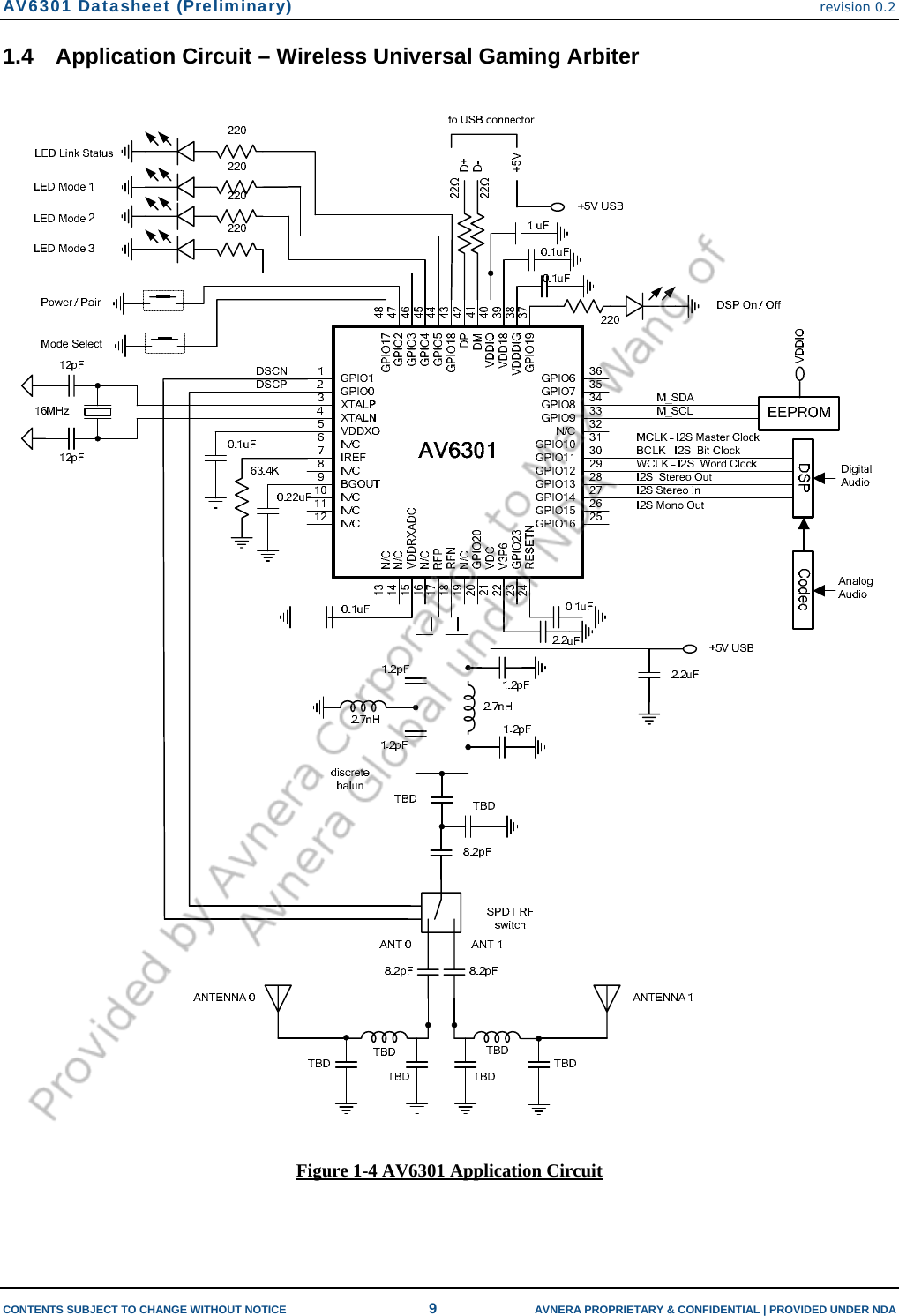
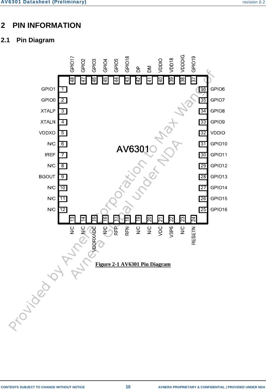
Datasheet