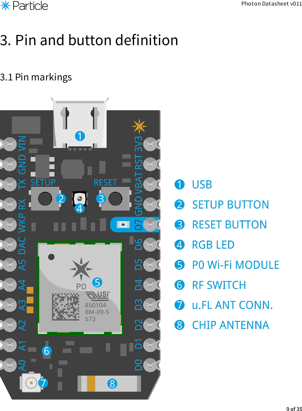
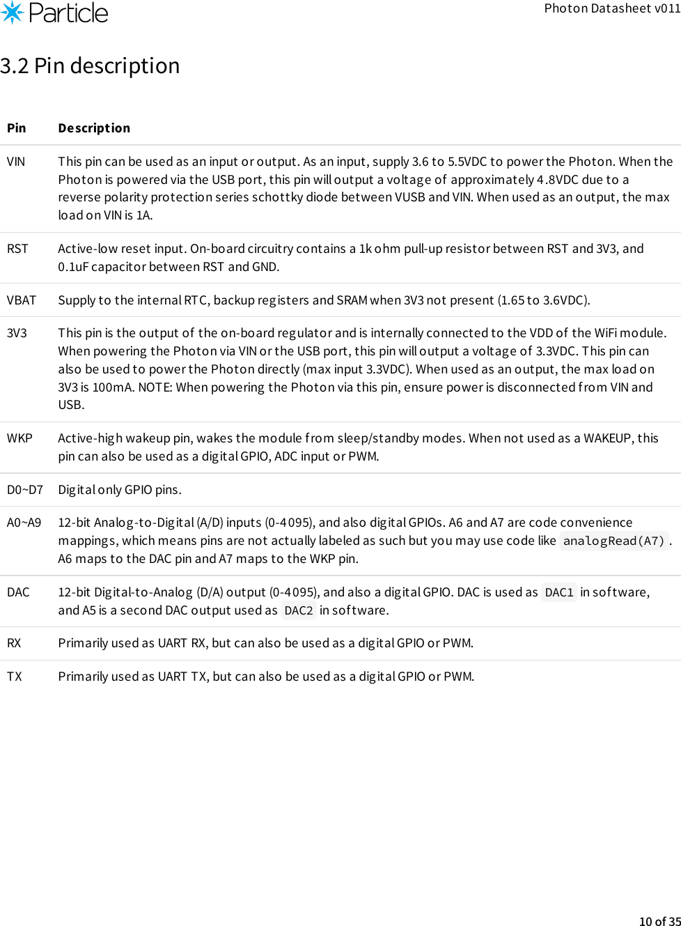
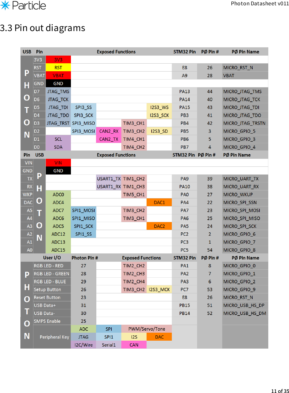
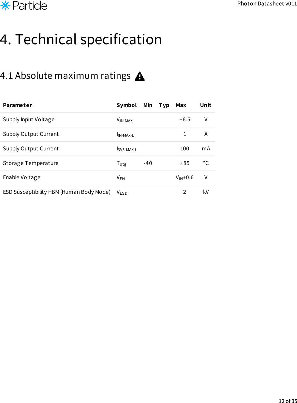
Particle PHOTON PHOTON User Manual photon datasheet v011 FCC md
Spark Labs, Inc., PHOTON photon datasheet v011 FCC md
UserManual.wiki
>
Particle
>
PHOTON User Manual
Users Manual
Navigation menu
Upload a User Manual
Namespaces
Wiki Guide
HTML
PDF
Info
Views
User Manual
Discussion / Help
Navigation
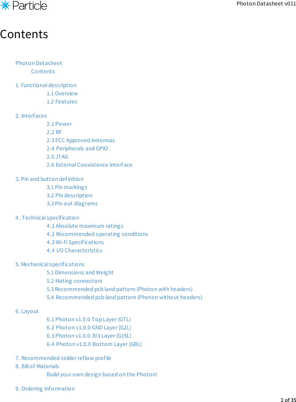

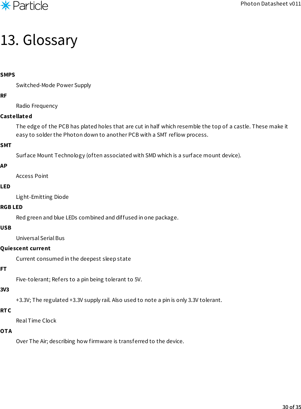
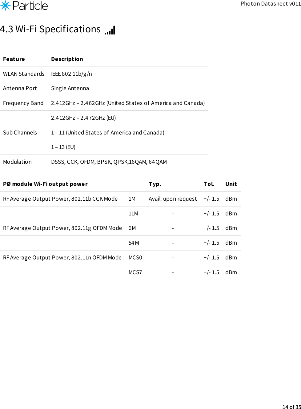
![Photon Datasheet v0112.3 FCC Approved AntennasAntenna T ype Manuf acturer MFG. Part # GainDipole antenna LumenRadio 104 -1001 2.15dBiChip antenna Advanced Ceramic X AT7020-E3R0HBA 1.3dBi2.4 Peripherals and GPIOThe Photon has ton of capability in a small footprint, with analog, digital and communication interf aces.Peripheral Type Qty Input(I) / Output(O) FT / 3V3Digital 18 I/O FT/3V3Analog (ADC) 8 I 3V3Analog (DAC) 2 O 3V3SPI 2 I/O 3V3I2S 1 I/O 3V3I2C 1 I/O FTCAN 1 I/O FTUSB 1 I/O 3V3PWM 9 O 3V3Notes: FT = 5.0V tolerant pins. All pins except A3 and DAC are 5V tolerant (when not in analog mode). If used as a 5V inputthe pull-up/pull-down resistor must be disabled. 3V3 = 3.3V max pins. PWM is available on D0, D1, D2, D3, A4, A5, WKP, RX, TX with a caveat: PWM timer peripheral is duplicated on two pins(A5/D2) and (A4/D3) for 7 total independent PWM outputs. For example: PWM may be used on A5 while D2 is used as aGPIO, or D2 as a PWM while A5 is used as an analog input. However A5 and D2 cannot be used as independentlycontrolled PWM outputs at the same time.[1] [2]3[1][2][3]6 of 35](https://usermanual.wiki/Particle/PHOTON/User-Guide-2659044-Page-6.png)
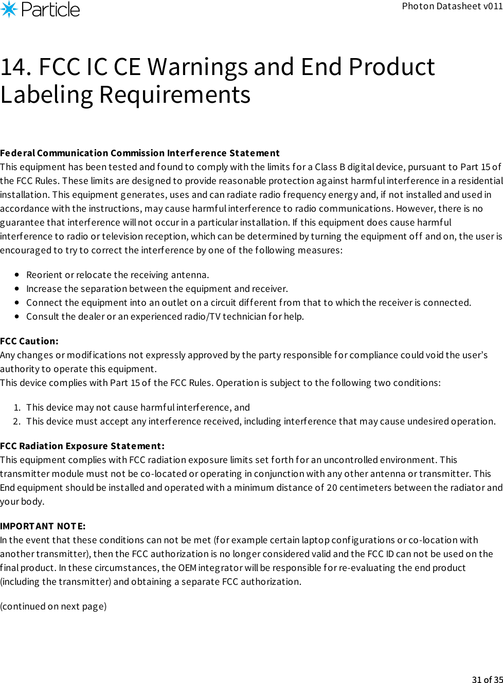
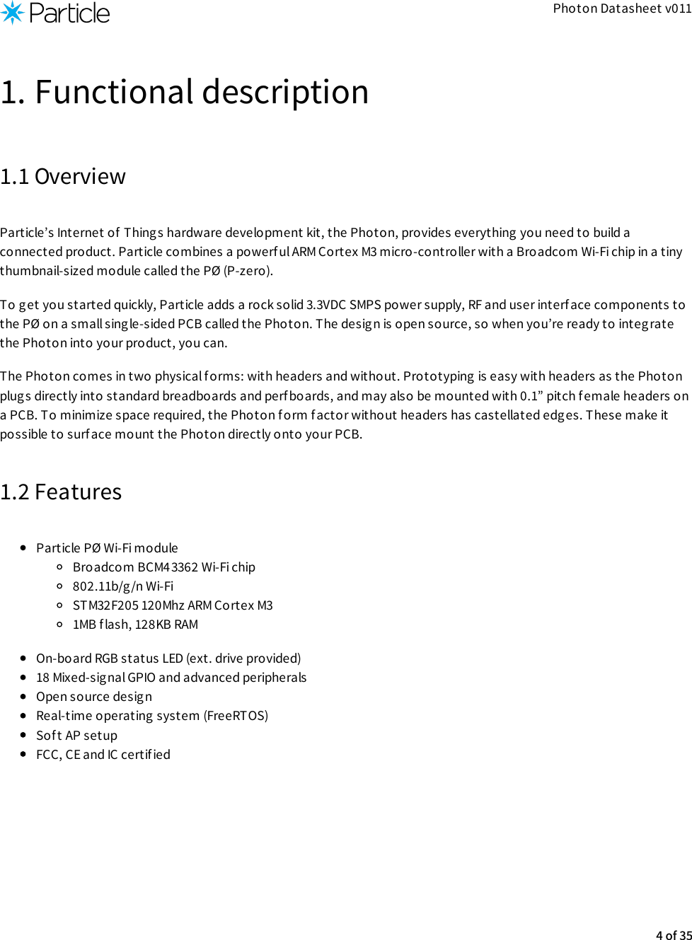
![Photon Datasheet v0112.5 JTAGPin D3 through D7 are JTAG interface pins. These can be used to reprogram your Photon bootloader or user firmwareimage with standard JTAG tools such as the ST-Link v2, J-Link, R-Link, OLIMEX ARM-USB-TINI-H, and also the FTDI-basedParticle JTAG Prog rammer.Photon Pin Description ST M32 Pin PØ Pin # PØ Pin Name Default InternalD7 JTAG_TMS PA13 44 MICRO_JTAG_TMS ~40k pull-upD6 JTAG_TCK PA14 40 MICRO_JTAG_TCK ~40k pull-downD5 JTAG_TDI PA15 43 MICRO_JTAG_TDI ~40k pull-upD4 JTAG_TDO PB3 41 MICRO_JTAG_TDO FloatingD3 JTAG_TRST PB4 42 MICRO_JTAG_TRSTN ~4 0k pull-up3V3 PowerGND GroundRST ResetNotes: Default state after reset f or a short period of time before these pins are restored to GPIO (if JTAG debugging is notrequired, i.e. USE_SWD_JTAG=y is not specified on the command line.A standard 20-pin 0.1” shrouded male JTAG interf ace connector should be wired as f ollows:[1][1]7 of 35](https://usermanual.wiki/Particle/PHOTON/User-Guide-2659044-Page-7.png)
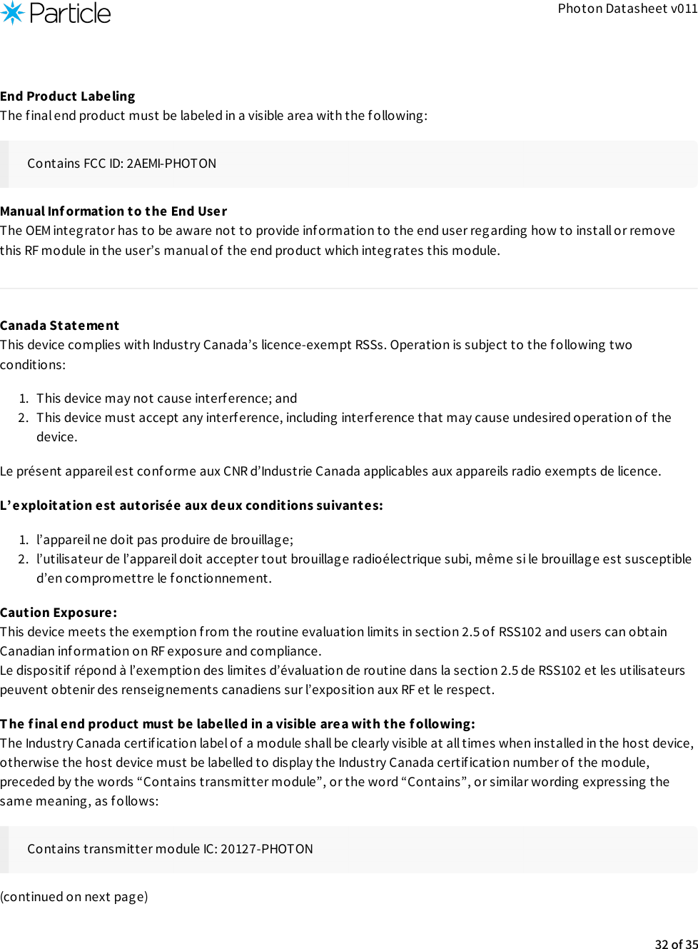
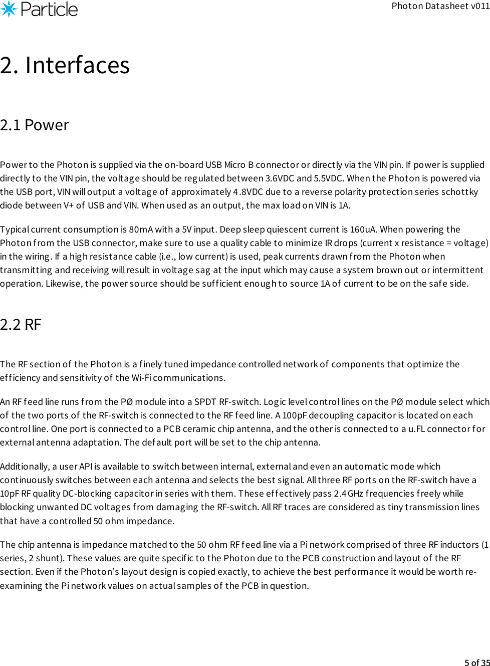
![Photon Datasheet v0114.2 Recommended operating conditions Parameter Symbol Min Typ Max UnitSupply Input Voltage V +3.6 +5.5 VSupply Input Voltage V +3.0 +3.3 +3.6 VSupply Output Voltage V +4 .8 VSupply Output Voltage V +3.3 VSupply Input Voltage V +1.65 +3.6 VSupply Input Current (VBAT) I 19 uAOperating Current (Wi-Fi on) I 80 100 mAOperating Current (Wi-Fi on) I 235 430 mAOperating Current (Wi-Fi on, w/powersave) I 18 100 mAOperating Current (Wi-Fi off ) I 30 40 mASleep Current (5V @ VIN) I 1 2 mADeep Sleep Current (5V @ VIN) I 80 100 uAOperating Temperature T -20 +60 °CHumidity Range Non condensing, relative humidity 95 %Notes: These numbers represent the extreme range of short peak current bursts when transmitting and receiving in802.11b/g/n modes at dif ferent power levels. Averag e TX current consumption in will be 80-100mA. These are very short average current bursts when transmitting and receiving. On average if minimizing f requencyof TX/RX events, current consumption in powersave mode will be 18mAIN3V3IN3V3VBATVBATIN avgIN pk [1] [1]IN avg [2]IN avgQsQdsop[1][2]13 of 35](https://usermanual.wiki/Particle/PHOTON/User-Guide-2659044-Page-13.png)
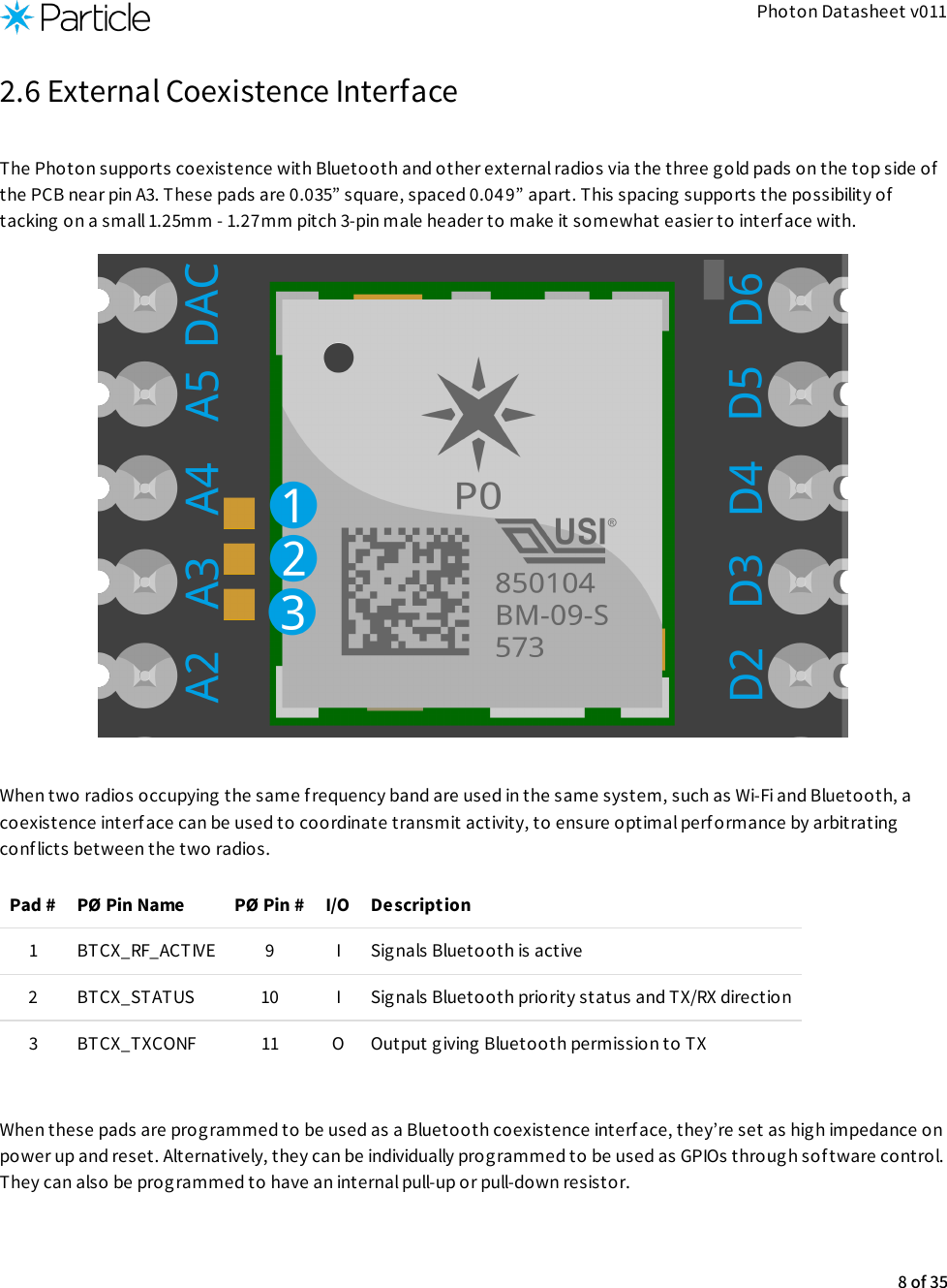
![Photon Datasheet v0114.4 I/O CharacteristicsThese specifications are based on the STM32F205RG datasheet, with reference to Photon pin nomenclature.Parameter Symbol Conditions Min Typ Max UnitStandard I/O input low level voltage V -0.3 0.28*(V -2)+0.8VI/O FT input low level voltage V -0.3 0.32*(V -2)+0.75VStandard I/O input hig h level voltage V 0.4 1*(V -2)+1.3V +0.3 VI/O FT input hig h level voltage V V > 2V 0.42*(V -2)+15.5 VV V ≤ 2V 0.4 2*(V -2)+15.2 VStandard I/O Schmitt trigg er voltagehysteresisV 200 mVI/O FT Schmitt trigger voltagehysteresisV 5% V mVInput leakag e current I GND ≤ V ≤ VGPIOs±1 µAInput leakag e current I R V = 5V, I/OFT3 µAWeak pull-up equivalent resistor R V = GND 30 4 0 50 k ΩWeak pull-down equivalent resistor R V = V 30 4 0 50 k ΩI/O pin capacitance C 5 pFNotes: FT = Five-volt tolerant. In order to sustain a voltage hig her than V +0.3 the internal pull-up/pull-down resistorsmust be disabled. Hysteresis voltage between Schmitt trig g er switching levels. Based on characterization, not tested in production. With a minimum of 100mV. Leakage could be higher than max. if neg ative current is injected on adjacent pins.IL 3V3[1] IL 3V3IH 3V3 3V3[1] IH 3V3 3V3IH 3V3 3V3[2]hys[2]hys 3V3[3][4] lkg io 3V3[4] lkg PU io[5] PU io[5] PD io 3V3IO[1] 3V3[2][3][4]15 of 35](https://usermanual.wiki/Particle/PHOTON/User-Guide-2659044-Page-15.png)
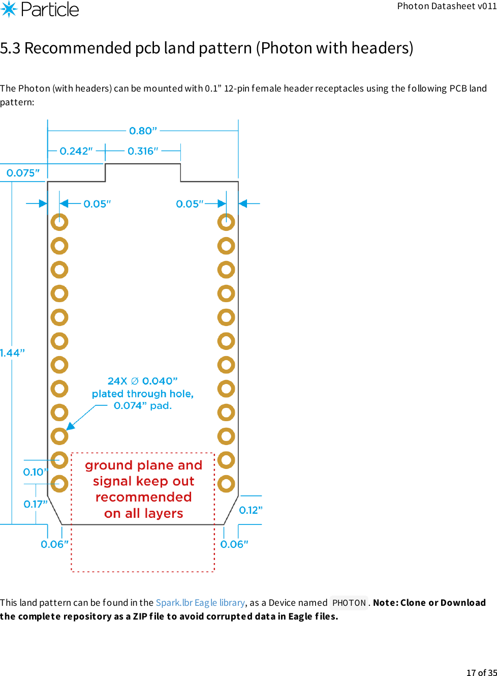
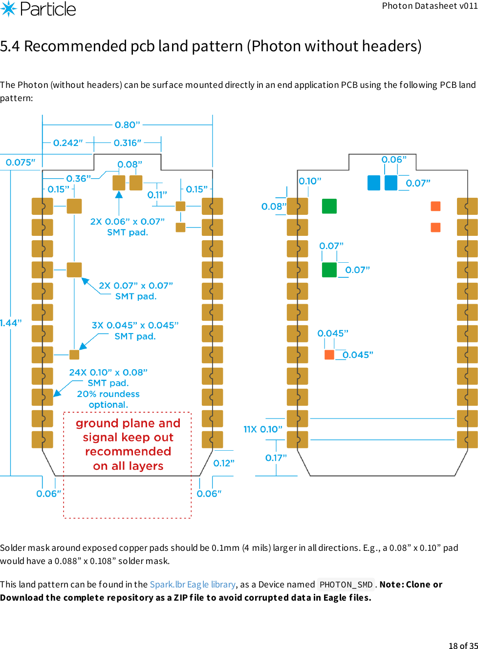
![Photon Datasheet v011 Pull-up and pull-down resistors are desig ned with a true resistance in series with switchable PMOS/NMOS. ThisPMOS/NMOS contribution to the series resistance is minimum (~10% order).5. Mechanical specifications5.1 Dimensions and WeightHeaders Dimensions in inches (mm) WeightWith 1.44 x 0.8 x 0.27 (36.58 x 20.32 x 6.86) 5 gramsWithout 1.44 x 0.8 x 0.17 (36.58 x 20.32 x 4.32) 3.7 grams5.2 Mating connectorsThe Photon (with headers) can be mounted with (qty 2) 12-pin single row 0.1” female headers. Typically these are0.335” (8.5mm) tall, but you may pick a taller one if desired. When you search for parts like these it can be difficult tonavigate the thousands of parts available.On Digikey.com, this section Rectangular Connectors - Headers, Receptacles, Female Sockets contains 36,000 of them. Narrow the search with: 12 positions, 1 row, 0.1” (2.54mm) pitch, Through Hole mountingtypes (unless you want SMT), and sort by Price Ascending. You may f ind something like this:Description MFG MFG Part Number12-pin 0.1” Female Header (Tin) Sullins Connector Solutions PPTC121LFBN-RC12-pin 0.1” Female Header (Gold) Sullins Connector Solutions PPPC121LFBN-RCYou may also search f or other types, such as reverse mounted (bottom side SMT) female headers, low profile types,machine pin, etc..[5]16 of 35](https://usermanual.wiki/Particle/PHOTON/User-Guide-2659044-Page-16.png)