Novatel Wireless NRMUNDP-1D UNDP-1PCI EXPRESS MINI CARD User Manual UNDP 1 Universal Notebook Data Platform User Guide
Novatel Wireless, Inc. UNDP-1PCI EXPRESS MINI CARD UNDP 1 Universal Notebook Data Platform User Guide
Contents
- 1. User Manual
- 2. USER MANUAL
- 3. User Manual 1
- 4. User Manual 2
- 5. Host User Manual
- 6. WWAN portion of User manual
WWAN portion of User manual
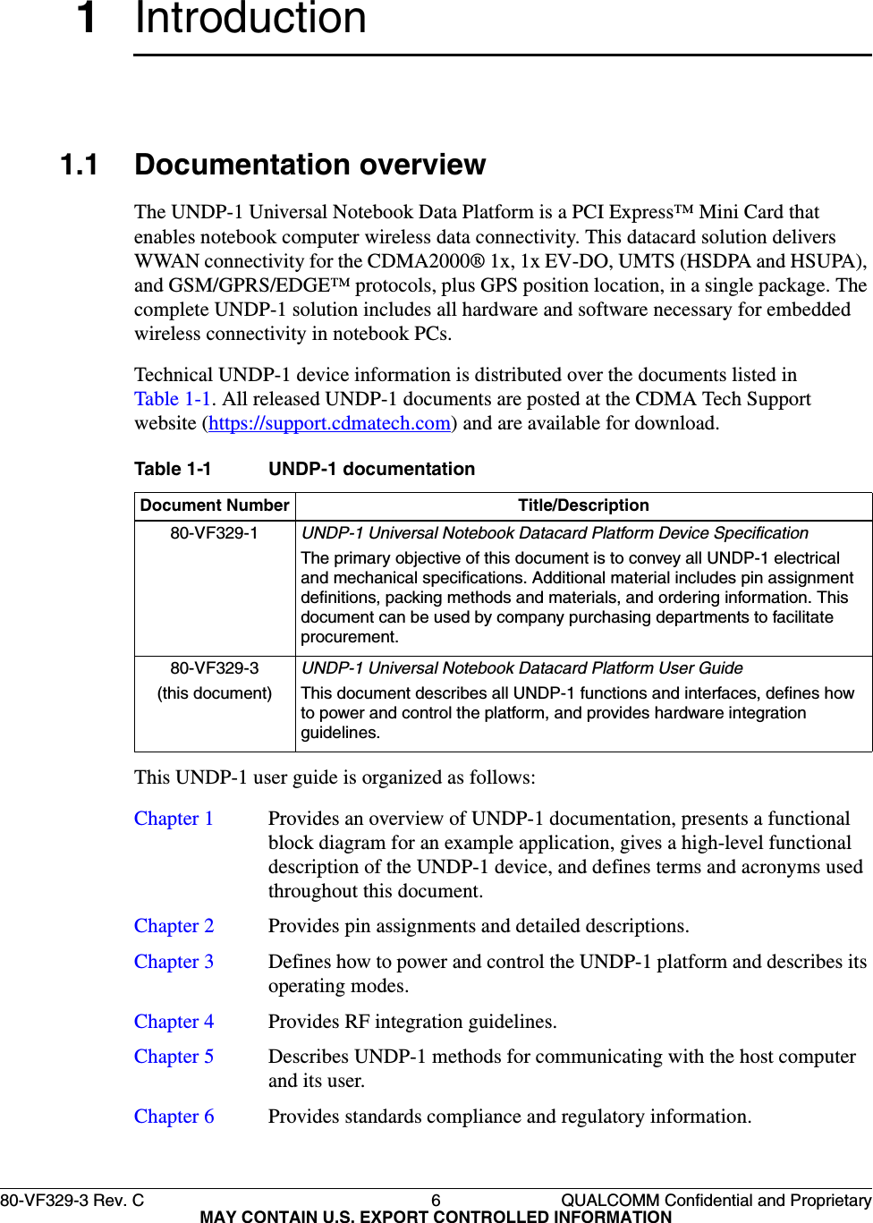
![80-VF329-3 Rev. C 7 QUALCOMM Confidential and ProprietaryMAY CONTAIN U.S. EXPORT CONTROLLED INFORMATIONUNDP-1 Universal Notebook Data Platform User Guide IntroductionTable 1-2 lists documents referred to throughout the UNDP-1 document-set; consult them for additional information.Table 1-2 Reference documentsRef No. Document[1] QUALCOMM WWAN Connection Manager API (80-VF219-1)[2] Supplement to Streaming Download Protocol (80-VF459-1)[3] Antenna Design Guidelines for Laptop and Notebook Computers (80-H2929-1)[4] FCC Regulations - CFR 47, Part1, 2, 15, 22 and 24[5] PCI Express Mini Card Electromechanical Specification, Revision 1.1[6] Universal Serial Bus Specification, Revision 2.0[7] Protection of Electrical and Electronic Parts, Assemblies, and Equipment(ANSI/ESD S20.20-1999)](https://usermanual.wiki/Novatel-Wireless/NRMUNDP-1D.WWAN-portion-of-User-manual/User-Guide-1186287-Page-7.png)
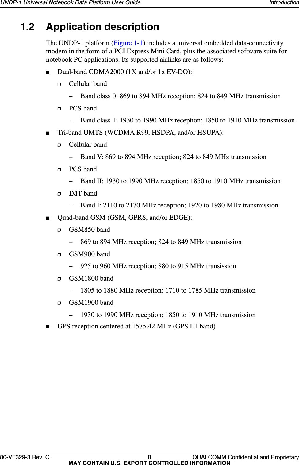
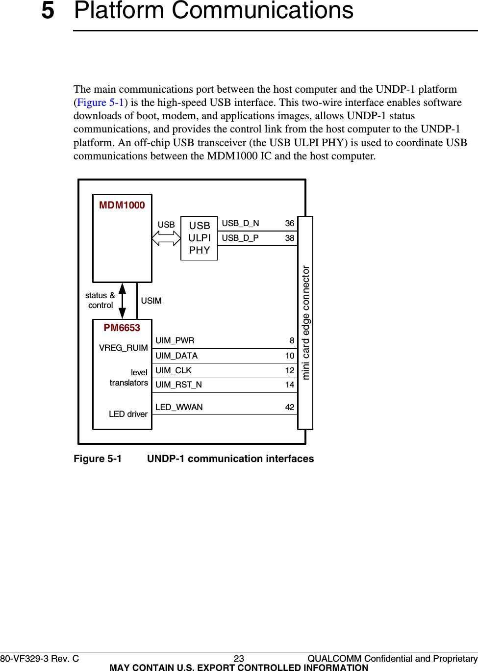
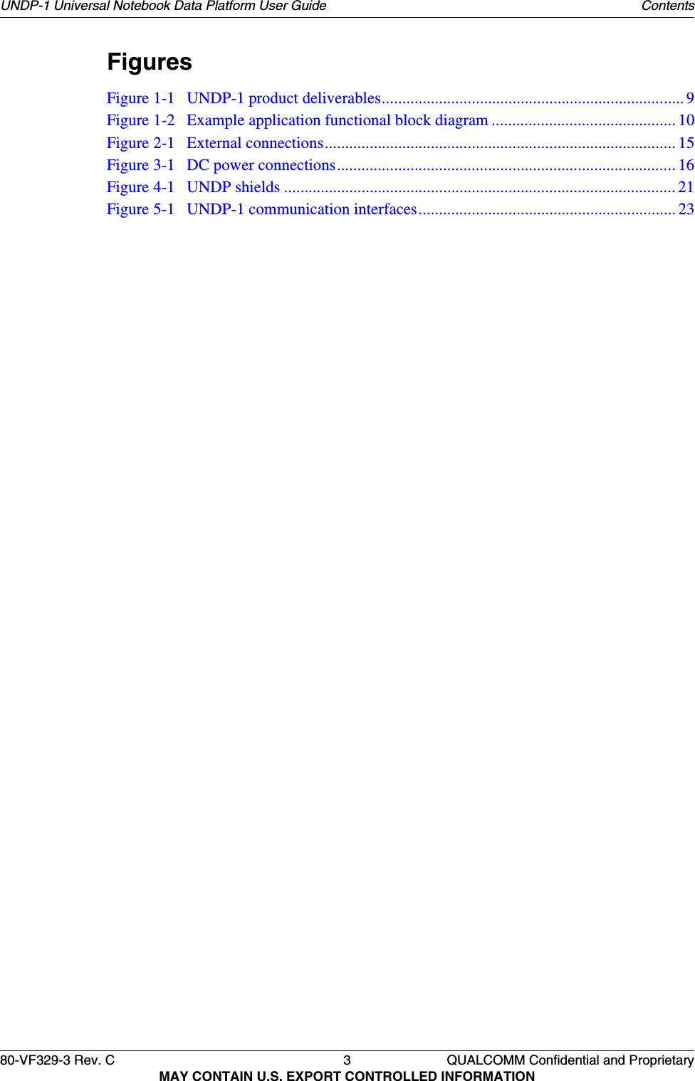
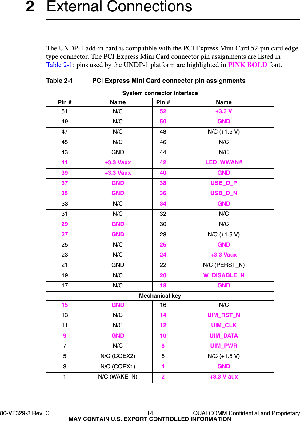
![80-VF329-3 Rev. C 10 QUALCOMM Confidential and ProprietaryMAY CONTAIN U.S. EXPORT CONTROLLED INFORMATIONUNDP-1 Universal Notebook Data Platform User Guide IntroductionA high-level hardware block diagram is shown in Figure 1-2. Two Hirose (U.FL-R-SMT) antenna connectors are provided for the following:1. The primary connector supports transmission and reception by the active CDMA, UMTS, or GSM transceiver.2. The secondary connector supports diversity reception by the active CDMA or UMTS link plus GPS reception.Figure 1-2 Example application functional block diagramThe antenna elements are typically integrated into the notebook computer and connected to the UNDP-1 module via flexible RF coaxial cables. This configuration, when adequate antenna performance is achieved, satisfies the PCI-SIG® standard requirements for PCI Express Mini Cards. Antenna performance requirements are defined in [3] and listed within Table 1-2.MDM1000RTR6285 Quad-band GSM Tx Quad-band UMTS Tx Tx power detector Quad-band GSM Rx Quad-band UMTS Rx (w/ Rx diversity) GPS RxPM6653Transmit outputchainsInput power managementVoltage regulatorsGeneral housekeepingUser interfacesIC interfacesprimary antenna connectorPrimary RFfront -endGSM Rx filtersUMTS IMT PRx filterSecondaryRF front-end w/ Rx BPFsTX BBRX0 BBRX1 BBVCTCXOsecondary antenna connectorRFR6500 Dual-band CDMA Rx (w/ Rx diversity) GPS RxCDMA Cell & PCS PRx filtersGPS filterstatus & controlstatus & controlstatus & controlUSBUSB ULPI PHYUSIMARM11ARM9DSP (x2)DDR SDRAMCDMA 1x, 1xEV-DOUMTS HSUPA & HSDPAGSM/GPRS/EDGEto RFICs & ULPIsupply voltagesTRK_LO_ADJTCXOUSIMVMAIN_3P3LED_WWANmini card edge connectorVDDLED driver32 Mbit NORUMTS IMT RX0CDMA + UMTS PCS RX0CDMA + UMTS Cell RX0UMTS IMT RX1GPS RXC + U Cell RX1C + U PCS RX1W_DISABLE_N](https://usermanual.wiki/Novatel-Wireless/NRMUNDP-1D.WWAN-portion-of-User-manual/User-Guide-1186287-Page-10.png)
![80-VF329-3 Rev. C 11 QUALCOMM Confidential and ProprietaryMAY CONTAIN U.S. EXPORT CONTROLLED INFORMATIONUNDP-1 Universal Notebook Data Platform User Guide IntroductionThe primary antenna is connected to its RF front-end circuits (a switch module, CDMA and UMTS duplexers, etc). In the transmit direction, these front-end circuits are driven by the transmit output chains: two chains support GSM low and high bands (GSM850 + GSM900 and GSM1800 + GSM1900); three chains support CDMA (Cell + PCS) and UMTS (Cell + PCS + IMT) operation. All baseband-to-RF processing - for all supported bands - is performed within the RTR6285 IC.The four GSM receive paths are filtered, then routed to the RTR6285 IC for processing. The CDMA and UMTS primary receive filtering is achieved within the front-end duplexers; the signals are then routed to either the RTR6285 IC (UMTS IMT) or the RFR6500 IC (CDMA and UMTS Cell + PCS) for RF-to-baseband processing.Like the primary antenna, the secondary antenna is connected to its own RF front-end circuits (a switch module, CDMA/UMTS filters, GPS filter, etc). The filtered signals are then routed to the appropriate RFIC for RF-to-baseband processing (RTR6285 IC for UMTS IMT; RFR6500 for CDMA and UMTS Cell + PCS and GPS).The MDM1000 device provides all the digital baseband processing, including modem functions for all the supported airlinks. Integrated MDM1000 functions include the ARM1136-J™ and ARM926EJ-S™ processor cores; two low-power, high-performance digital signal processor (DSP) cores; and 32 MB stacked dual data rate (DDR) synchronous dynamic random access memory (SDRAM). UICC (RUIM/USIM) is supported via an offboard UICC connector that is implemented per the PCI Express Mini Card specification, version 1.1. The UNDP-1 UICC interface is compliant with GSM 11.12 and ISO/IEC 7816-3 standards.In addition to the PCI Express Mini Card edge connector, board-level pads are provided for interfacing to a JTAG fixture. With its 4 MB of NOR flash memory and 32 MB of RAM (stacked DDR-SDRAM inside the MDM1000), the UNDP-1 supports a new code storage architecture via the QUALCOMM Data Loader (QDL). The Advanced Mobile Suscriber Software (AMSS) image is stored on the PC file system and downloaded to the UNDP-1 device RAM at system startup. NOR flash memory contains a boot image to support the initialization and configuration of the UNDP-1 hardware system, including the RF calibration items. It then enumerates on the USB, and the host computer downloads the embedded software and configuration memory items over the USB using QDL.Software interfaces that were developed for QUALCOMM chipsets are supported by the UNDP-1 product. The QDL data card interface ISOD describes the C API functions that PC software applications must use to interface with UNDP-1; see [1] listed within Table 1-2 for details. The supplement to the streaming download protocol specification describes the high-speed download protocol; see [2] within the same table for details.The UNDP-1 platform includes the PM6653 power management IC to detect and validate the applied DC power source, coordinate system powerup and powerdown actions, generate all the required on-board supply voltages, implement the primary on-board clock sources, and provide several secondary functions (such as driving the status LED).](https://usermanual.wiki/Novatel-Wireless/NRMUNDP-1D.WWAN-portion-of-User-manual/User-Guide-1186287-Page-11.png)
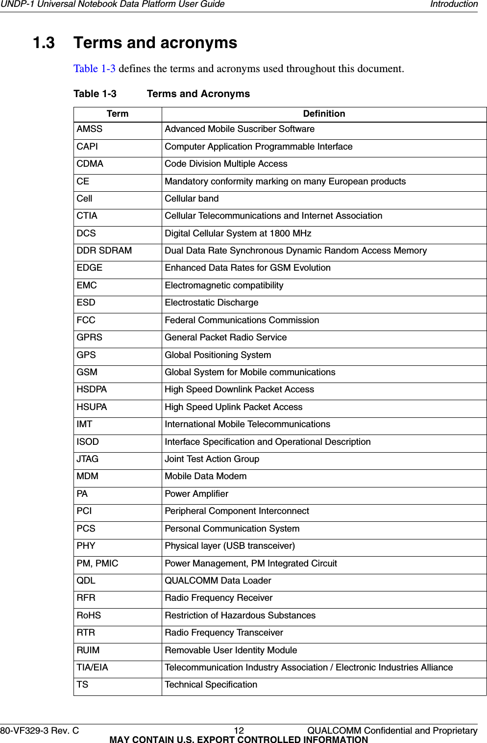
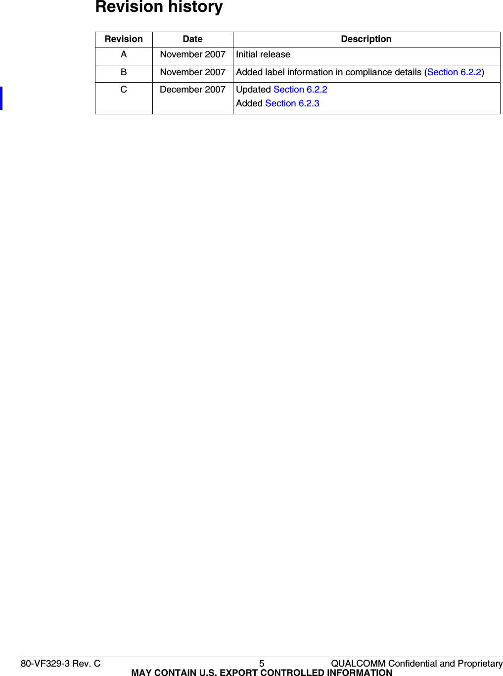
![80-VF329-3 Rev. C 21 QUALCOMM Confidential and ProprietaryMAY CONTAIN U.S. EXPORT CONTROLLED INFORMATIONUNDP-1 Universal Notebook Data Platform User Guide RF Integration4.4 Shielding and interferenceShielding is an extension of the system ground and must be installed to prevent interference between the host computer and the UNDP-1 platform. The platform is fully shielded (Figure 4-1), in accordance with FCC regulations (see [4] listed in Table 1-2). Figure 4-1 UNDP shieldsNOTE These UNDP shields must not be removed.The host PC is a hostile environment for RF transceivers, making the shields absolutely necessary. Potential interference sources include the following:■Noise or ripple on the DC power supply voltage input lines, including transients due to switching-mode power supplies or host operating mode changes.■High-speed digital logic transistions – The fast rising and falling edges include high frequency harmonics that can fall into the UNDP Rx and/or Tx passbands. Host circuits most likely to cause problems are the microprocessor, memory, and its displays and display drivers.■Clocks – Also due to their high-speed transitions■Other wireless devices, whether integrated into the host PC or external, such as WLAN (802.11) and Bluetooth devices. Transmit channels and their associated wideband noise can jam the UNDP receivers, and even their LO frequencies, digital logic, or clock signals can be disruptive.](https://usermanual.wiki/Novatel-Wireless/NRMUNDP-1D.WWAN-portion-of-User-manual/User-Guide-1186287-Page-21.png)