Novatel Wireless CNN0301 1XRTT Multi-Band M2M OEM Module User Manual CNN0301IG001 HS 3001
Novatel Wireless Inc. 1XRTT Multi-Band M2M OEM Module CNN0301IG001 HS 3001
UserManual.wiki
>
Novatel Wireless
>
CNN0301 User Manual
>
Integration Guide
Contents
1.
User Manual
2.
Integration Guide
Integration Guide
Navigation menu
Upload a User Manual
Namespaces
Wiki Guide
HTML
PDF
Info
Views
User Manual
Discussion / Help
Navigation
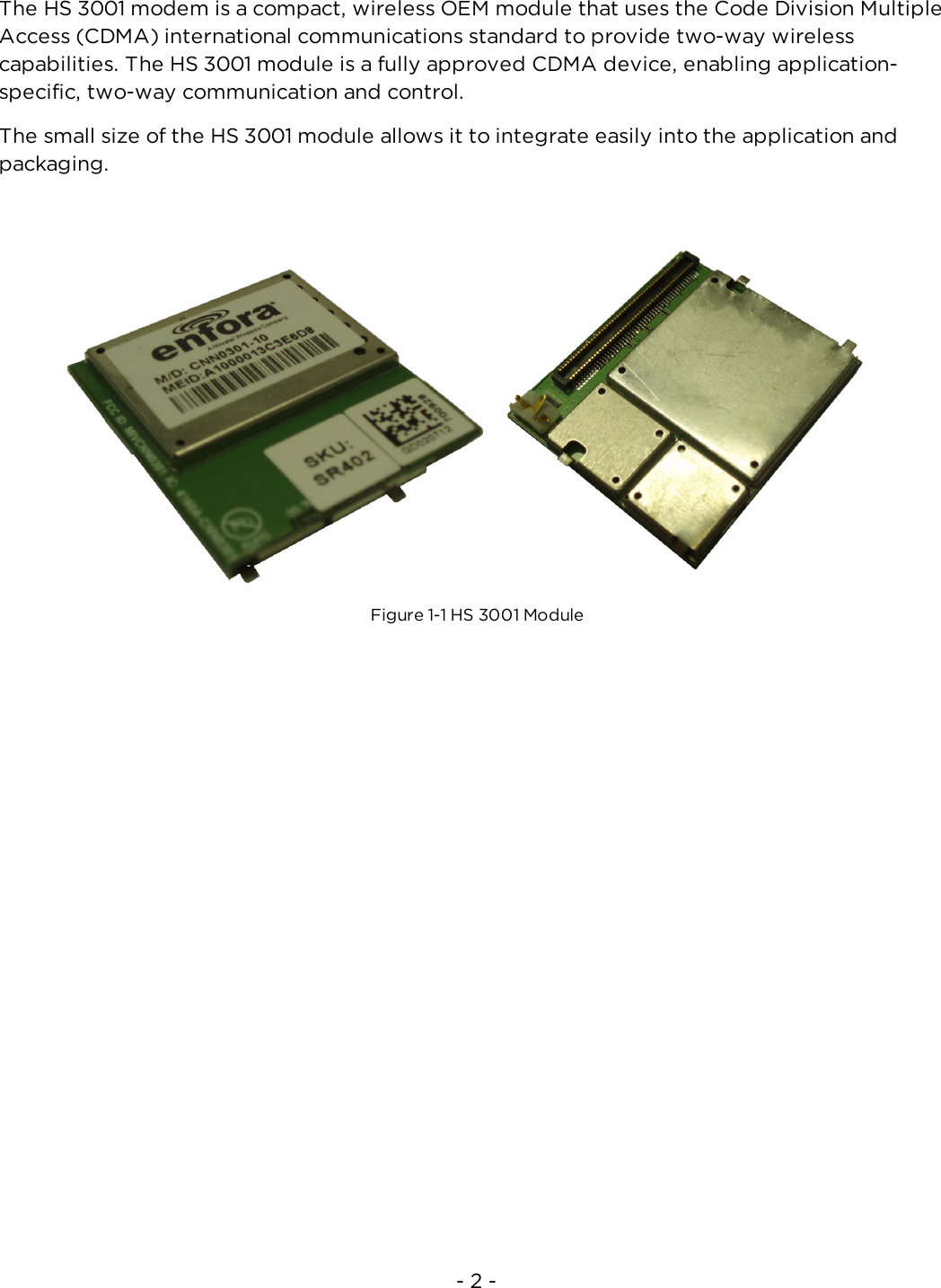
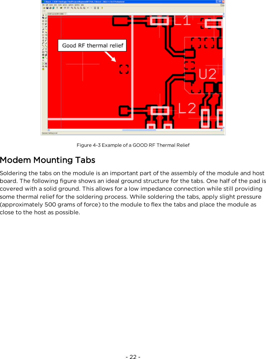
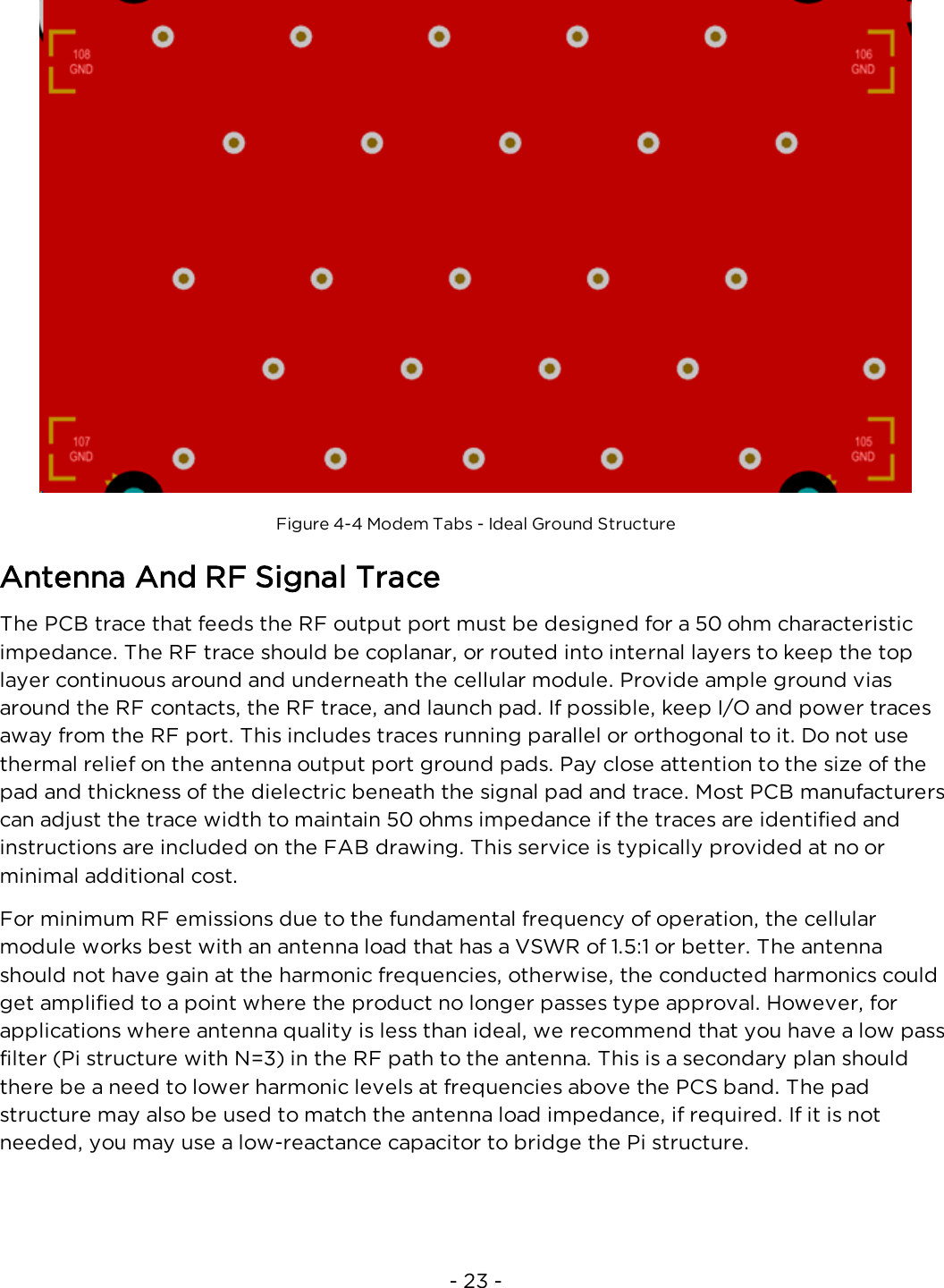
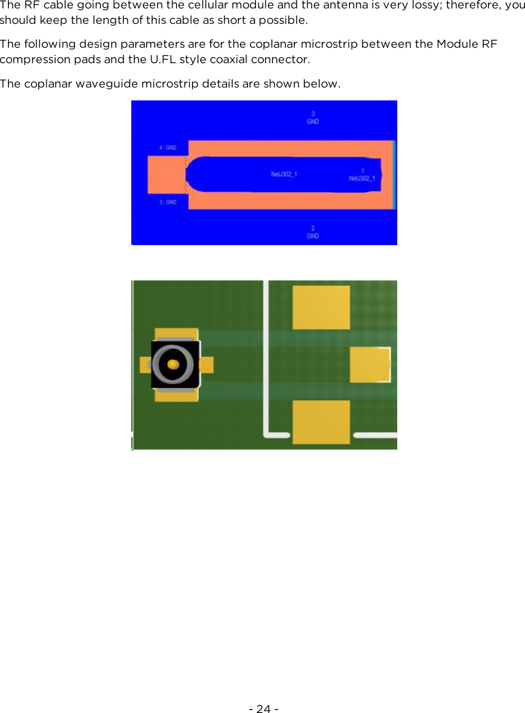
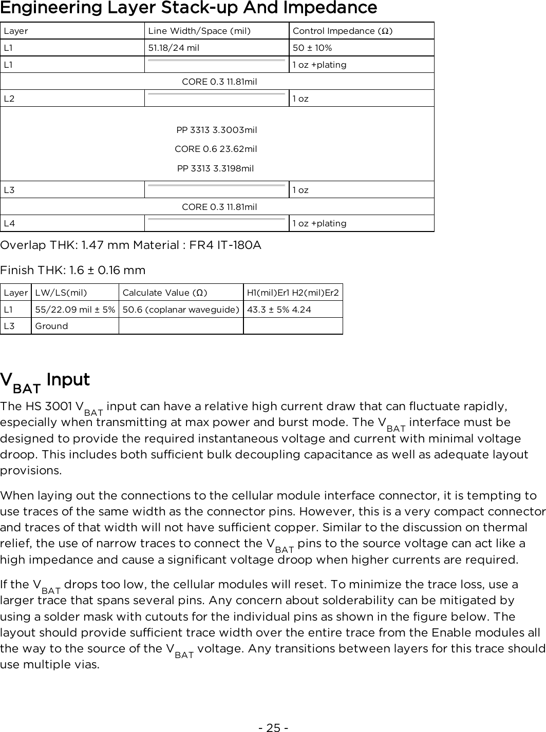
![- iii -Warranty Information[Revised: 11/11/2010]This warranty applies to (a) products sold directly by Novatel Wireless M2M, unless a differentwarranty is specified in a written agreement between Novatel Wireless M2M and thepurchaser; and (b) products sold to end users through a distributor authorized by NovatelWireless M2M, but only where the authorized distributor does not provide a separatewarranty on such products, and Novatel Wireless M2M has agreed to provide this warranty tosuch end users. If you purchased the product from an authorized distributor, please checkwhether this warranty from Novatel Wireless M2M, or a separate warranty from thedistributor, applies to your purchase. This warranty does not apply to any (i) accessories orbatteries for the products; or (ii) demonstration samples or prototypes of the products. Unlessotherwise provided in a written agreement between Novatel Wireless M2M and thepurchaser, all such accessories, batteries, samples or prototypes are provided by NovatelWireless M2M AS IS without any warranty of any kind.Novatel Wireless M2M warrants to the original purchaser of the product from NovatelWireless M2M or its authorized distributor (as applicable) that, for a period of one (1) yearfrom the date of shipment of the product from Novatel Wireless M2M, the product hardwarewill be substantially free from defects in material or workmanship under normal operation, andthe product firmware will perform substantially in accordance with the productdocumentation provided by Novatel Wireless M2M. Novatel Wireless M2M does not warrantthat (a) the product hardware or firmware will meet the purchaser's requirements; (b) theoperation of the product hardware or firmware will be uninterrupted or error-free; or (c) theproduct, when integrated in, or combined with, other products or software not supplied byNovatel Wireless M2M, will continue to perform substantially in accordance with the productdocumentation. This limited warranty is for the benefit of the original purchaser, and is nottransferable.During the warranty period, Novatel Wireless M2M, at its expense and in its sole discretion,will repair the product, or replace the product with a corresponding or equivalent product, ifit is determined to have a covered defect, provided that the purchaser first notifies NovatelWireless M2M (directly or through its authorized distributor from which the product waspurchased) of any such defect, furnishes Novatel Wireless M2M with a proof of purchase (ifrequired), requests and obtains a return merchandize authorization (RMA) number fromNovatel Wireless M2M, and returns the product under that RMA to Novatel Wireless M2M (or,at Novatel Wireless M2M's option, to its authorized distributor), with the shipping chargesbeing prepaid by purchaser. If, upon reasonable examination of the returned product, NovatelWireless M2M does not substantiate the defect claimed by purchaser, or determines that thedefect is not covered under this limited warranty, Novatel Wireless M2M will not be requiredto repair or replace the product, but may instead reship the product to the purchaser (or, atNovatel Wireless M2M's option, to its authorized distributor where the product can be made](https://usermanual.wiki/Novatel-Wireless/CNN0301.Integration-Guide/User-Guide-2007016-Page-4.png)