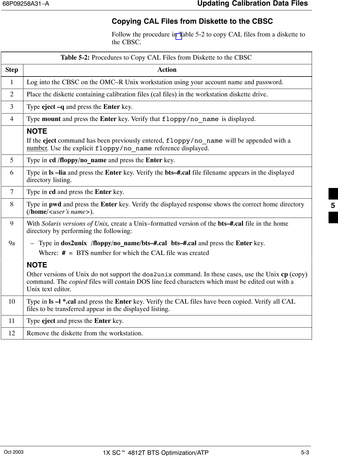
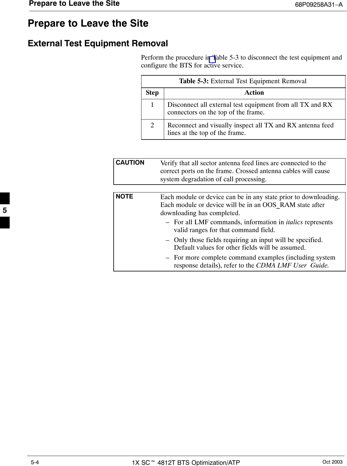
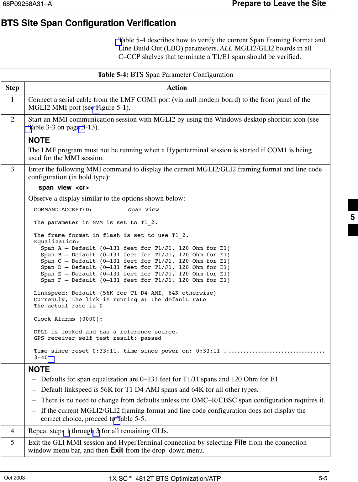
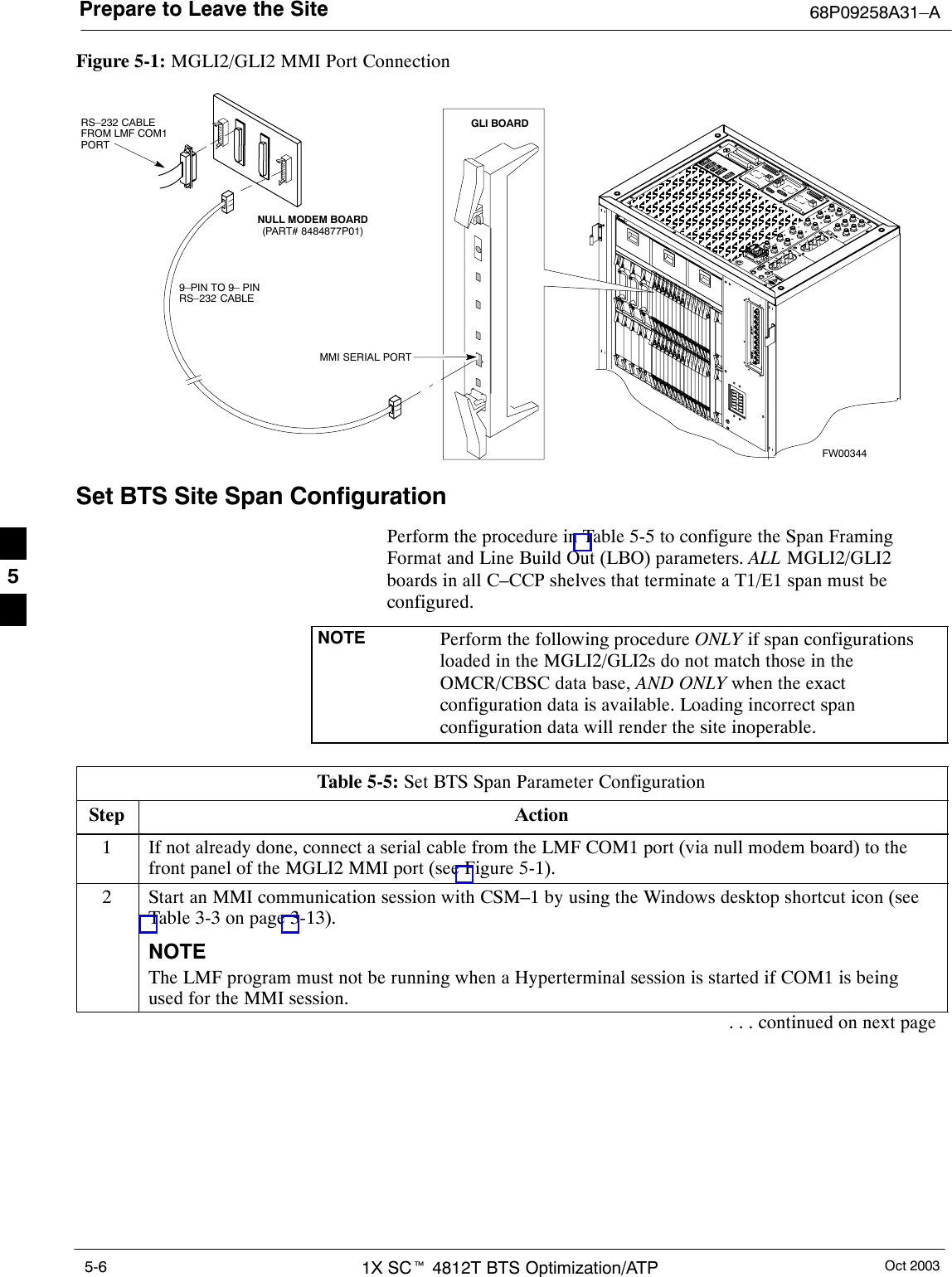
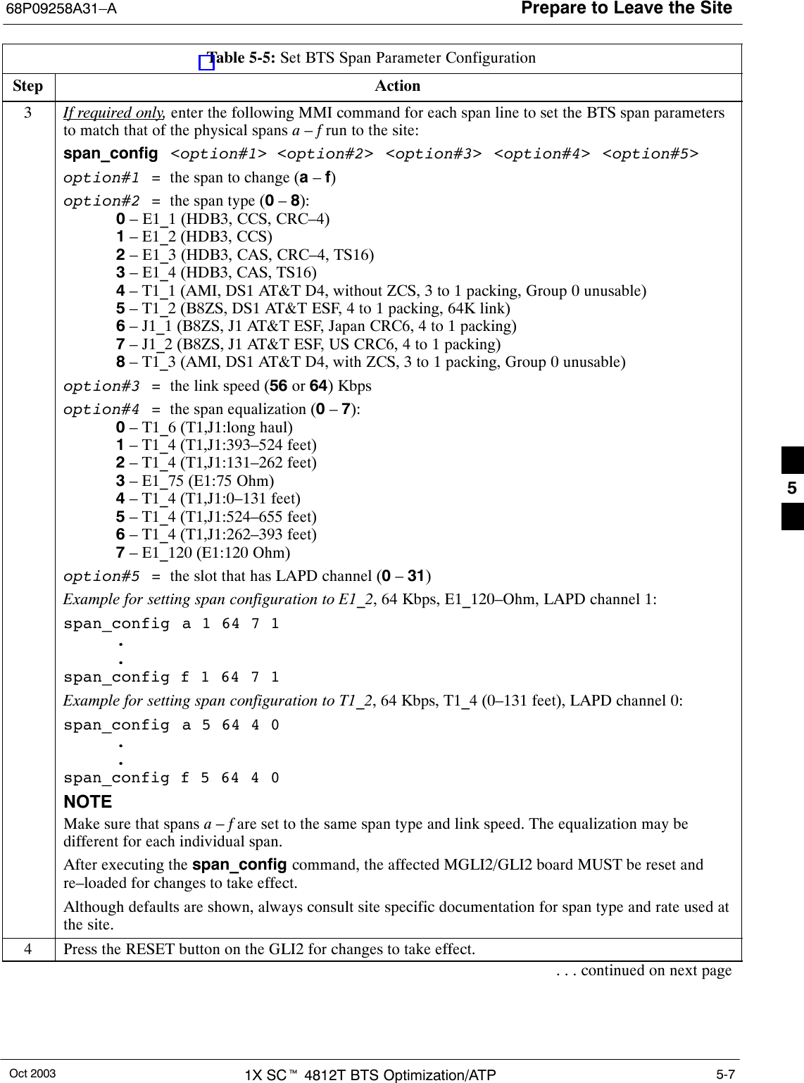
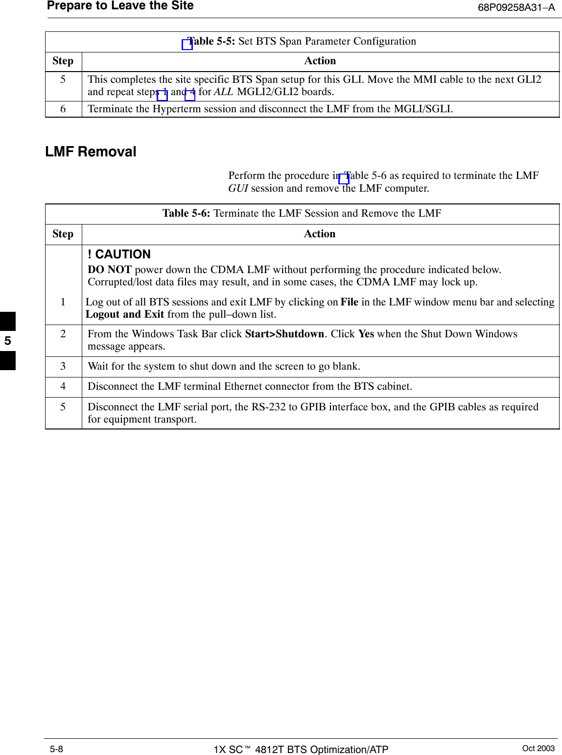
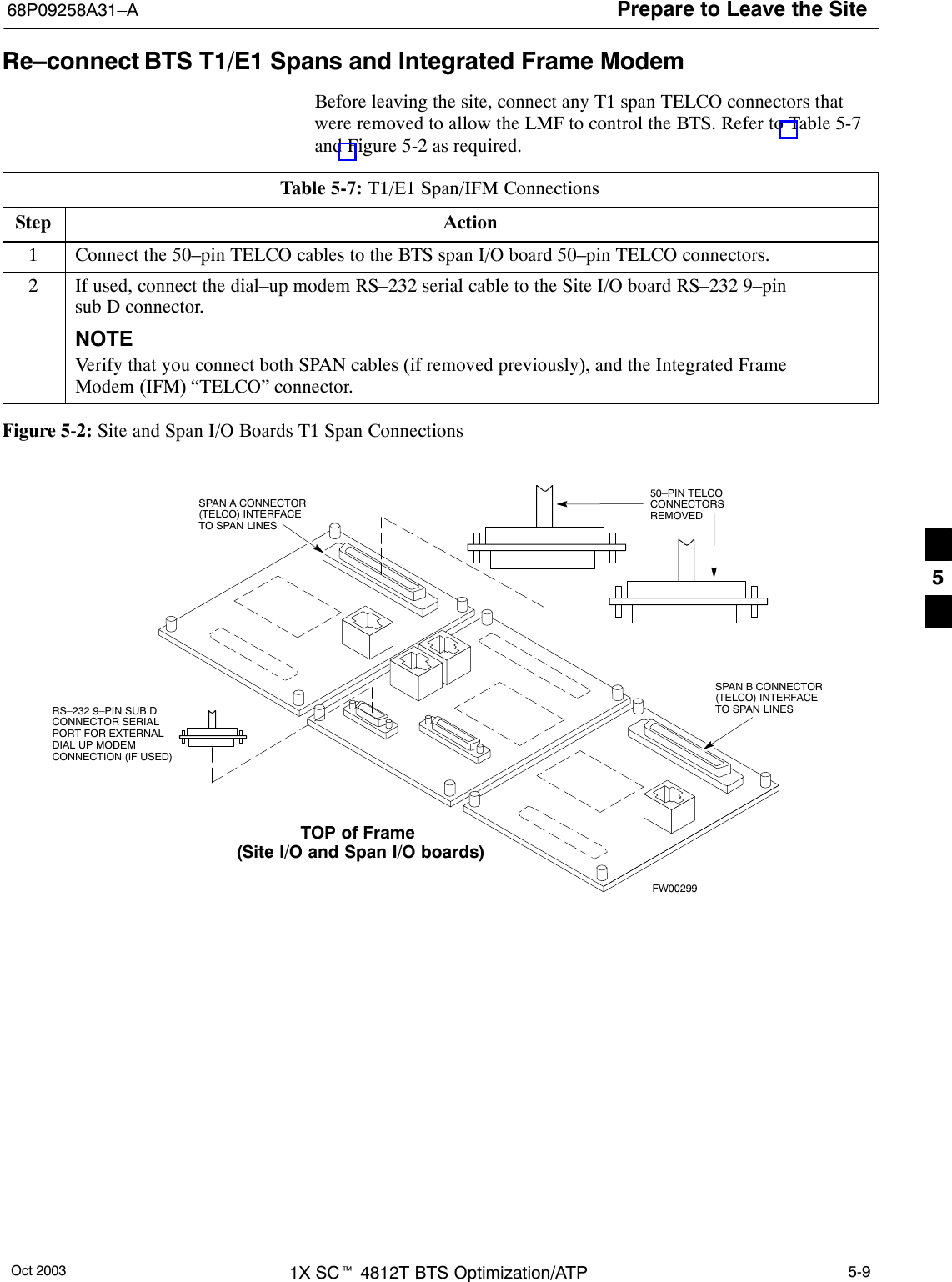
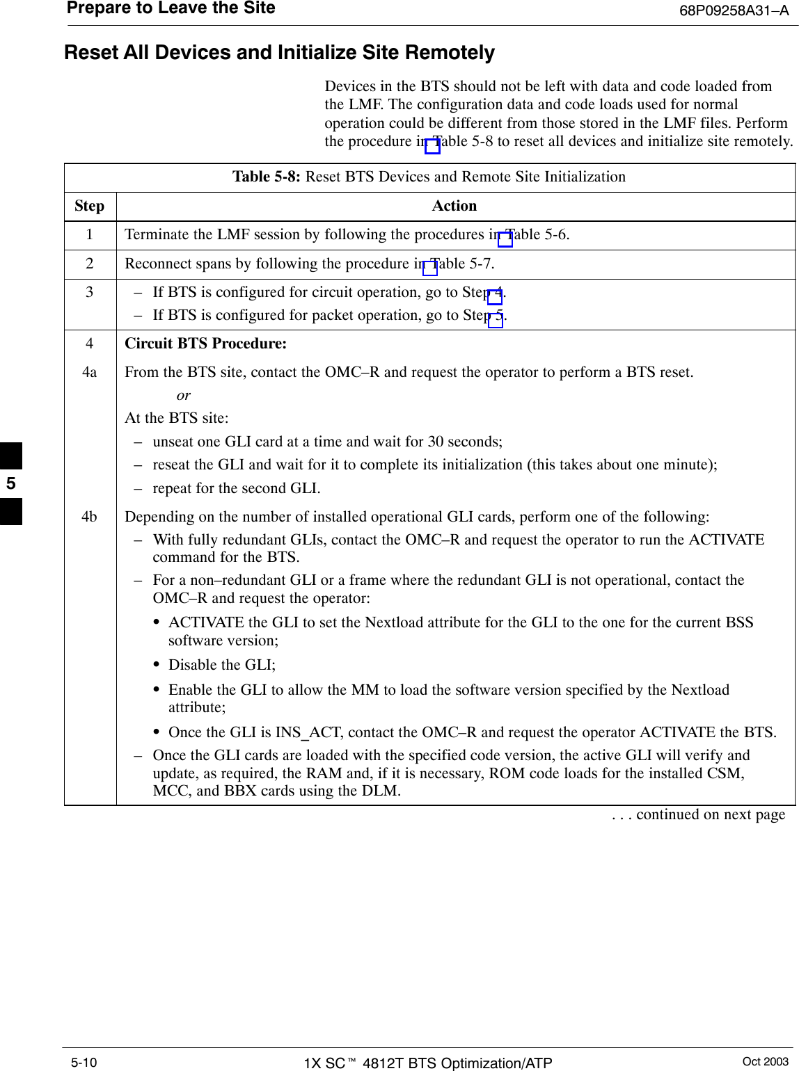
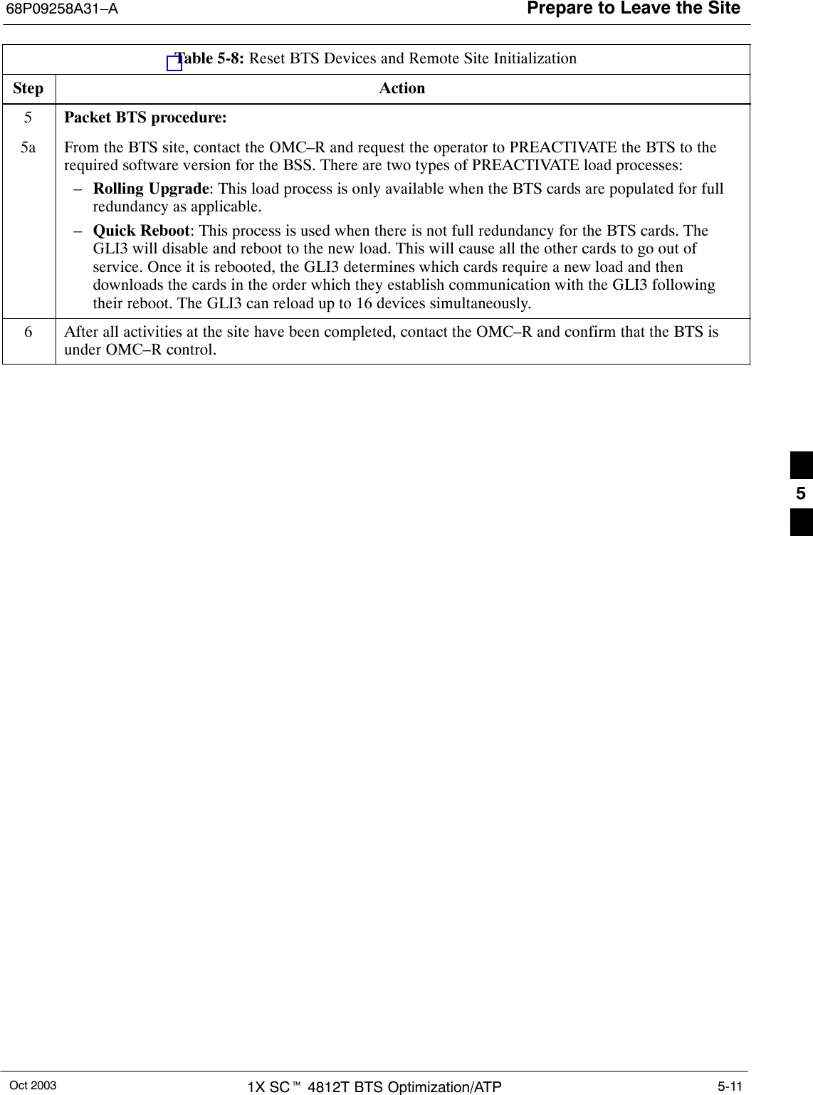
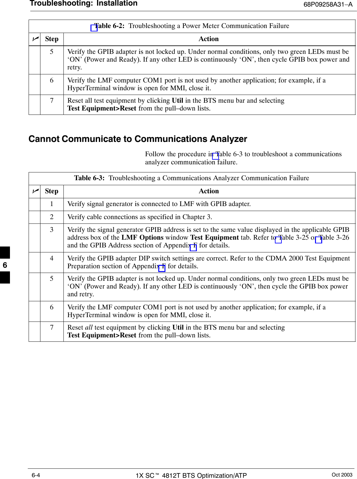
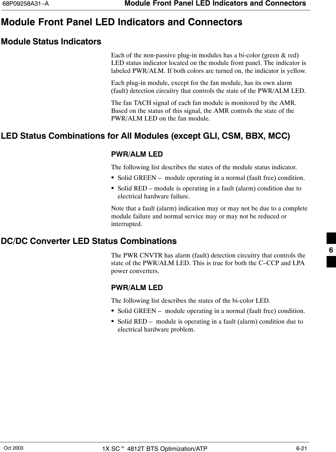
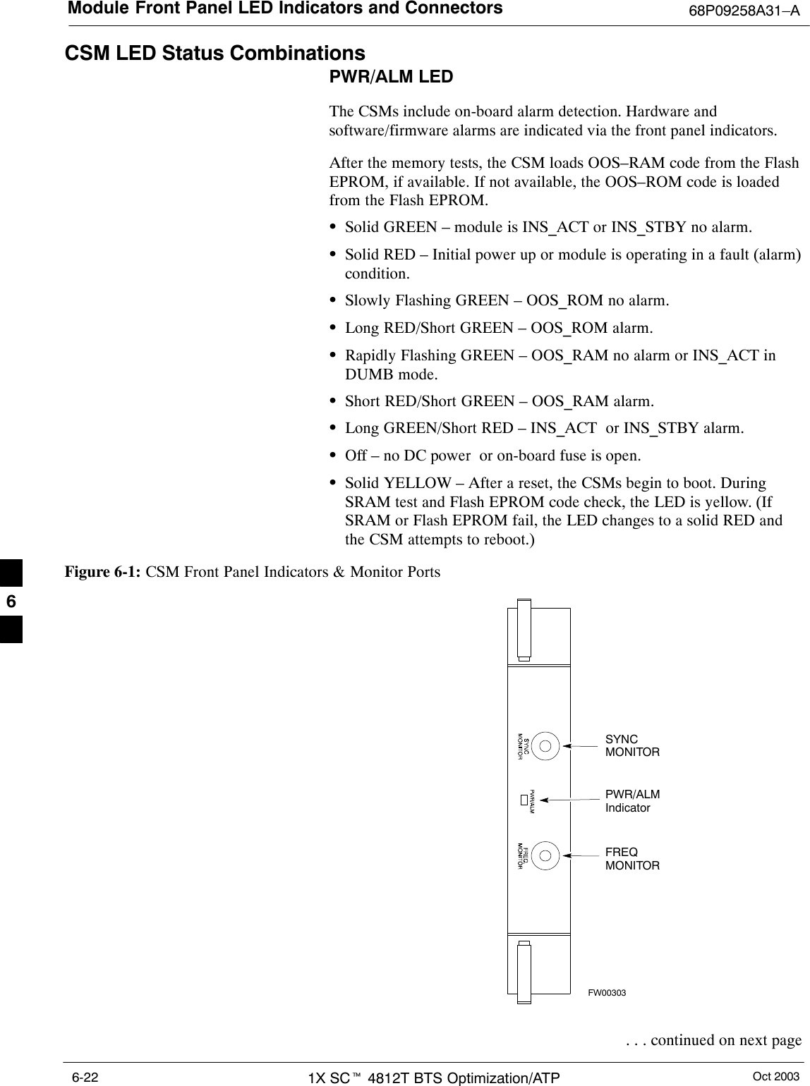
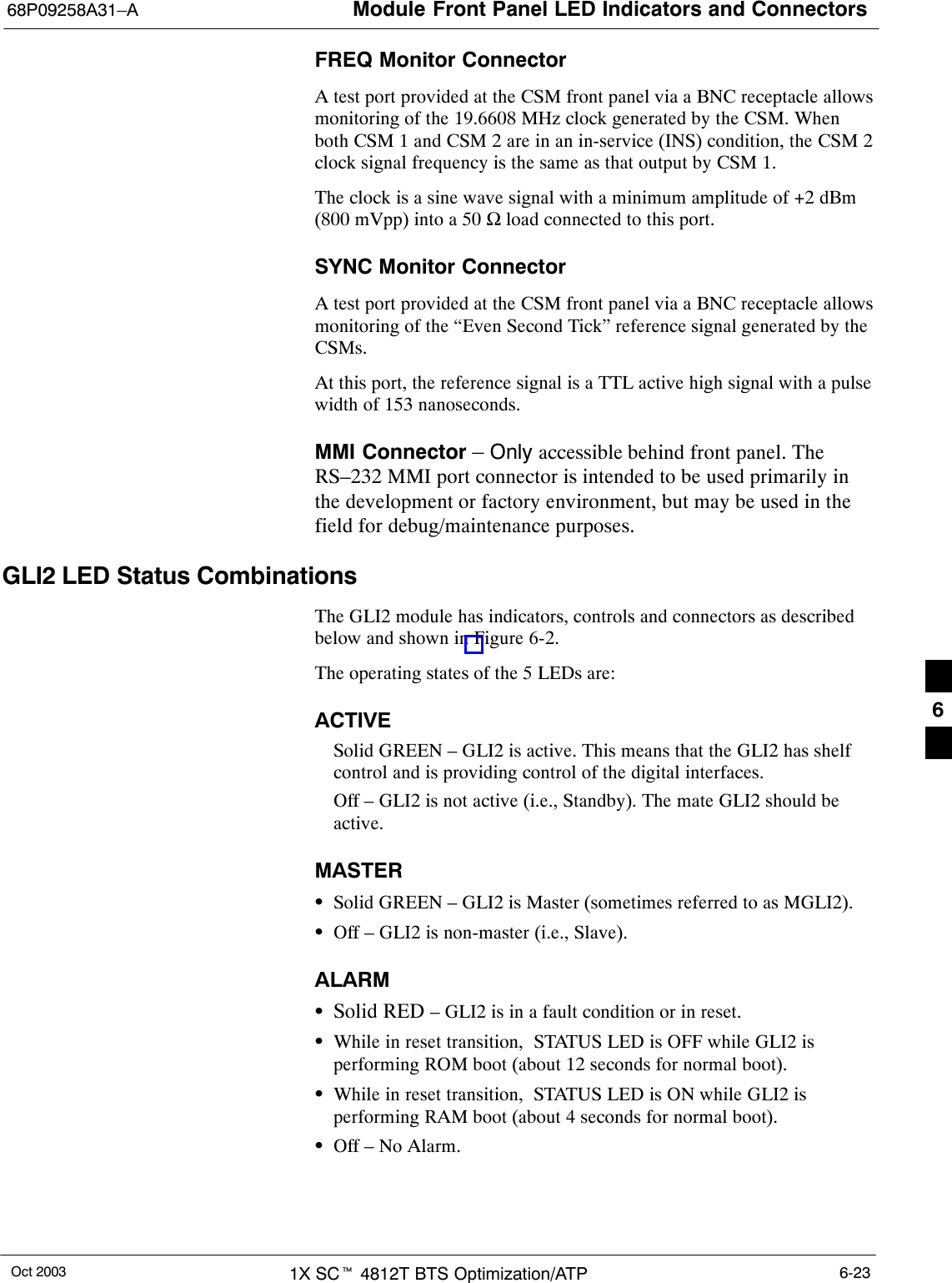
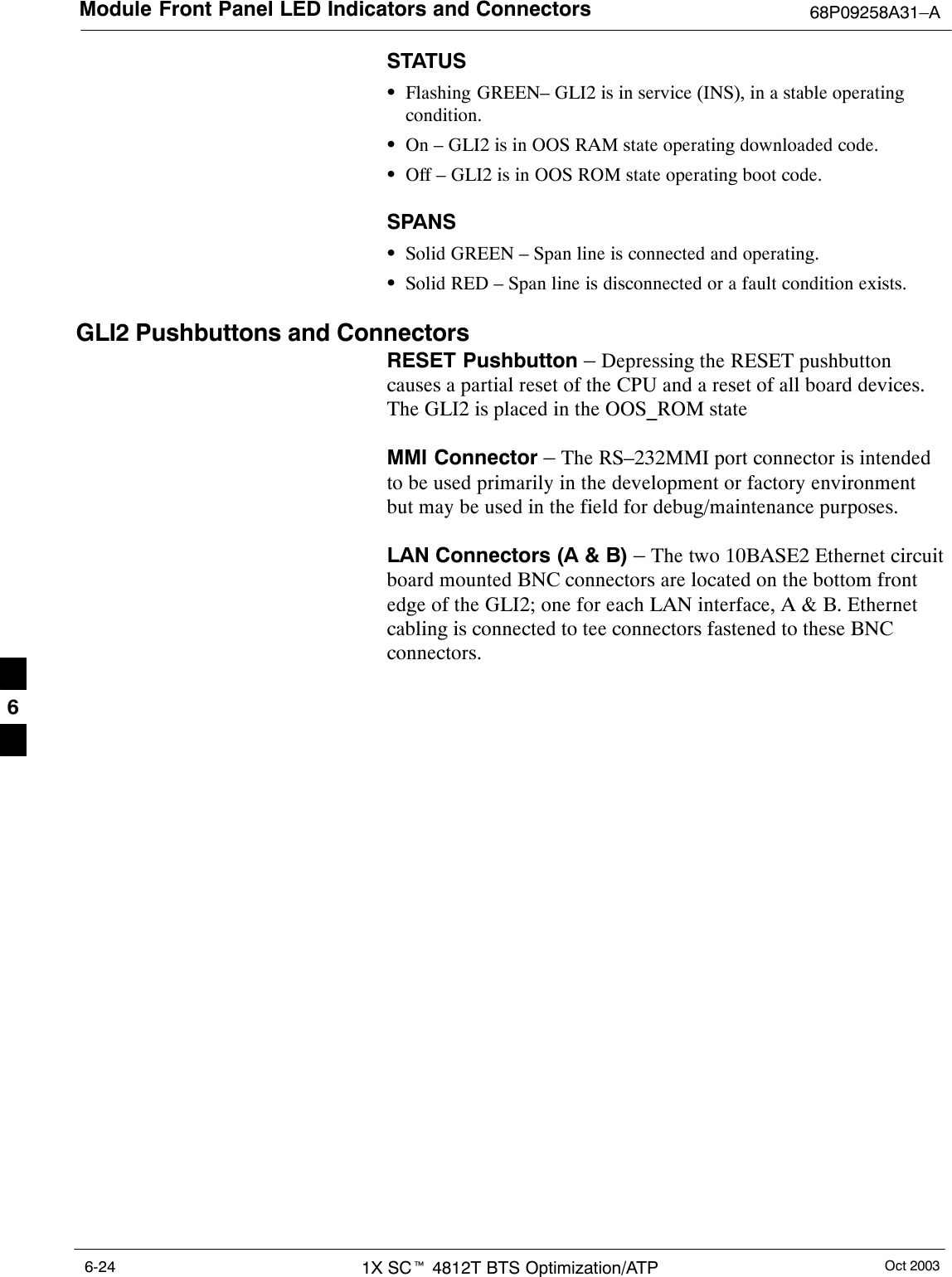
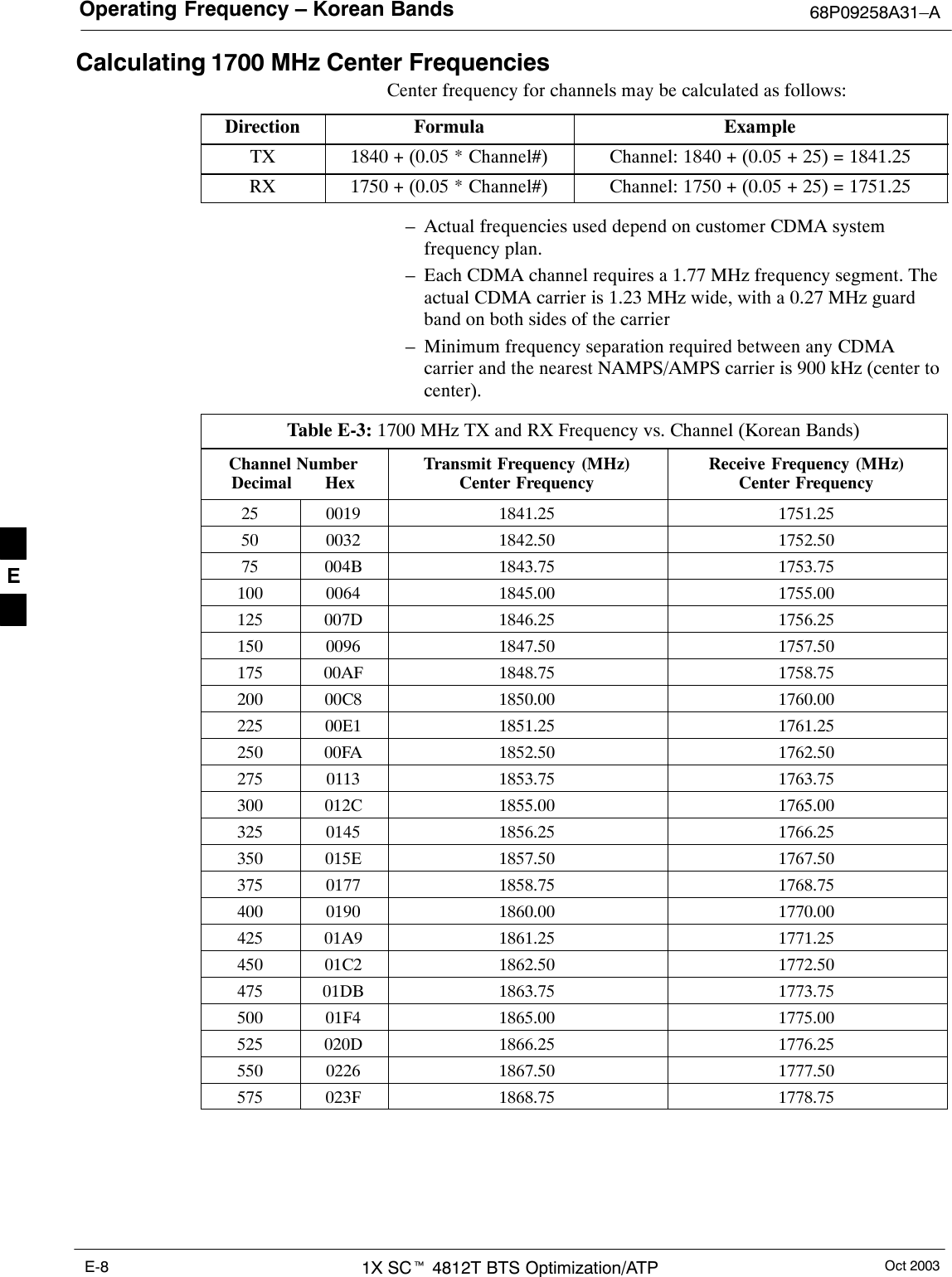
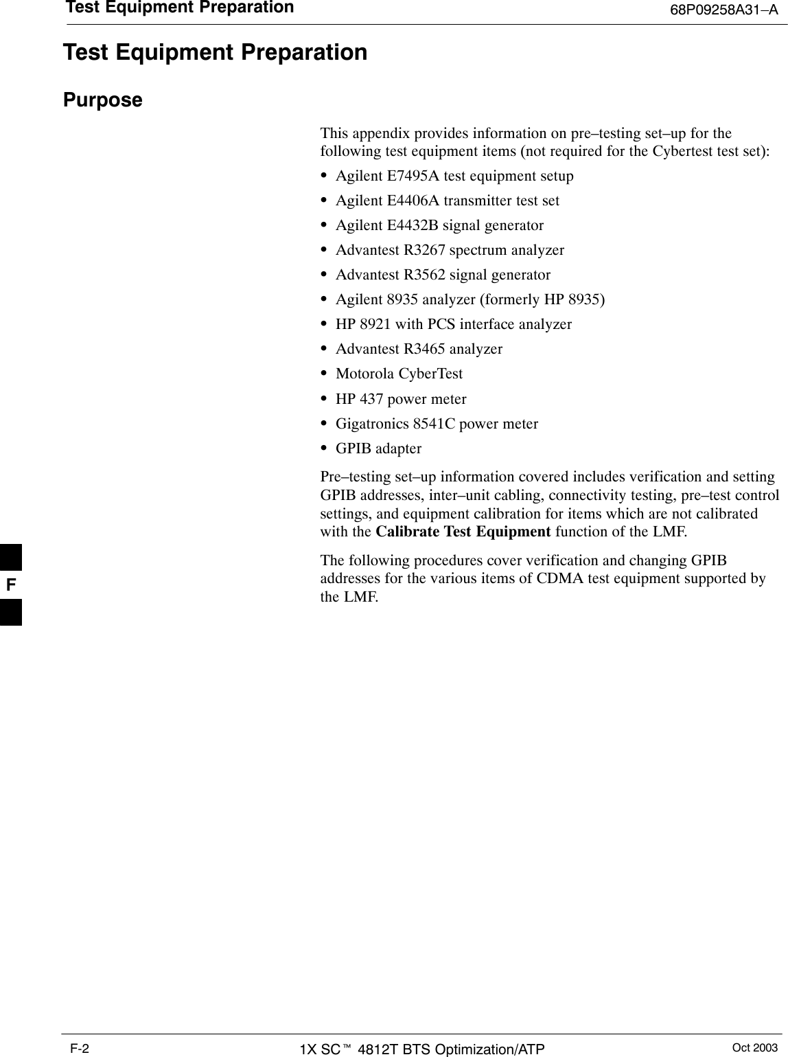
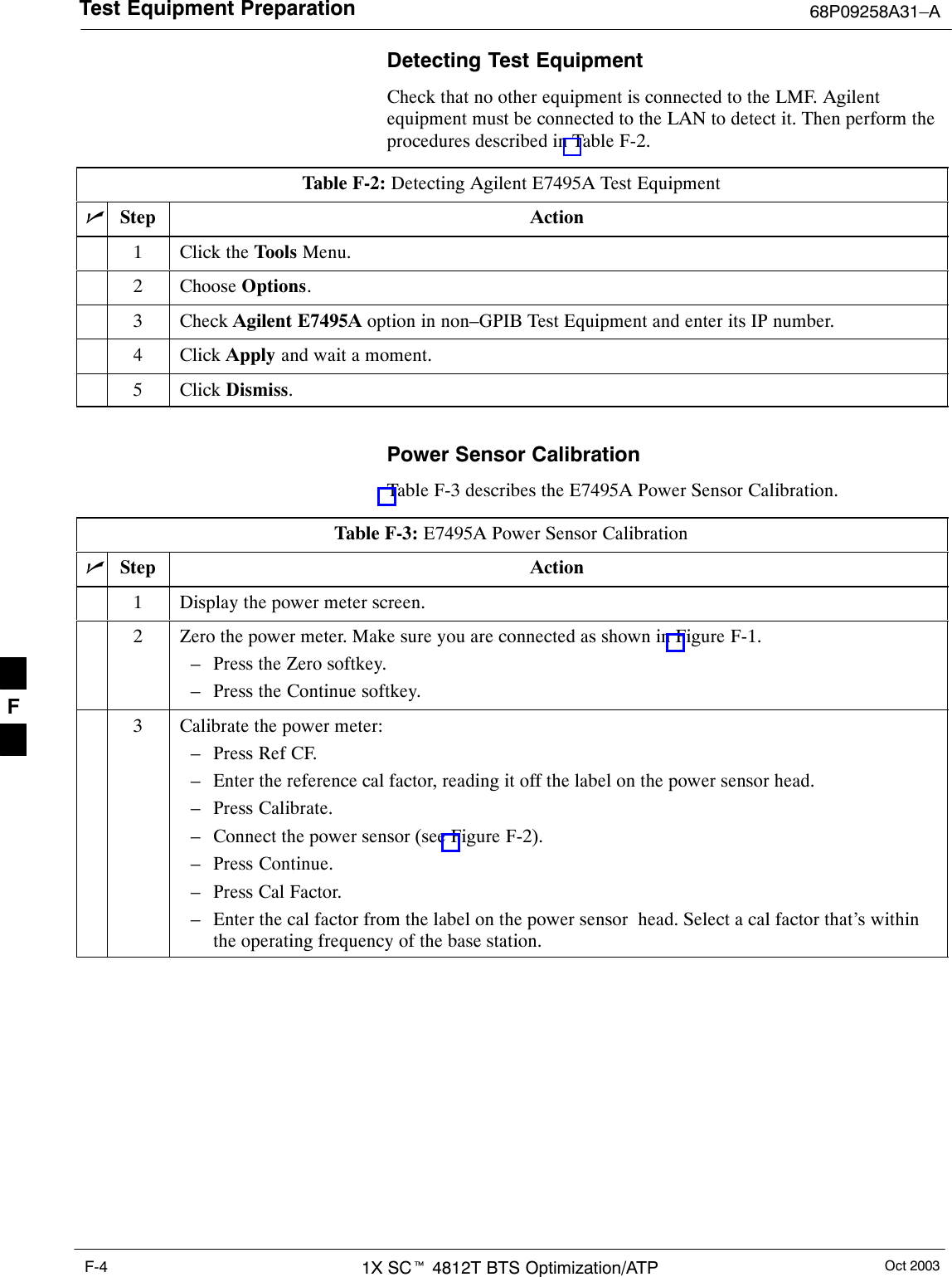
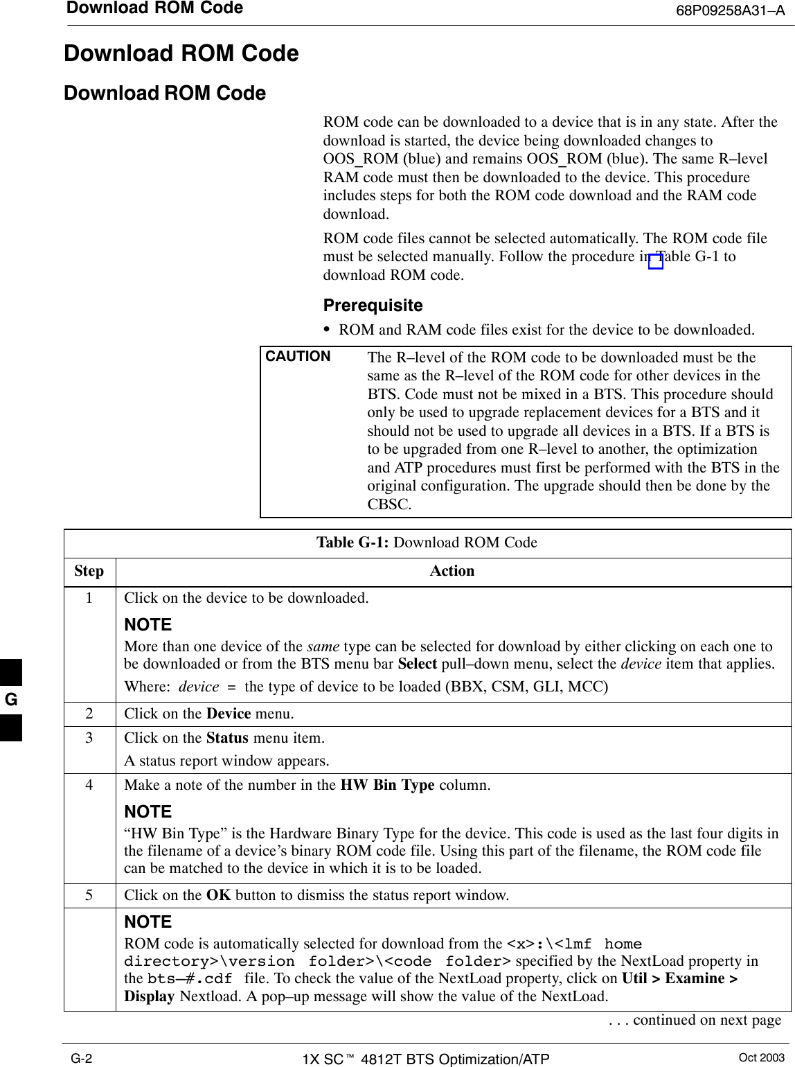
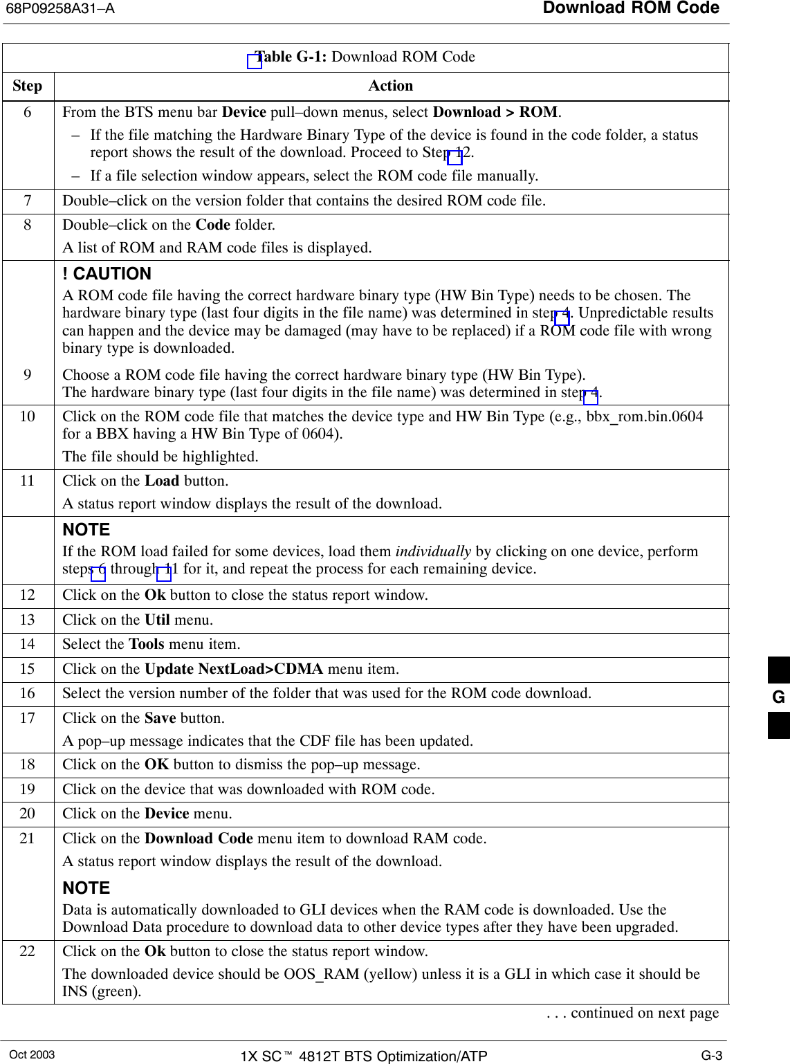
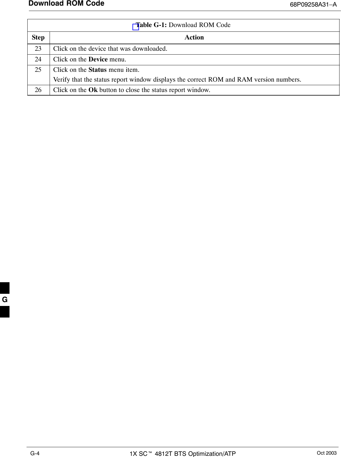
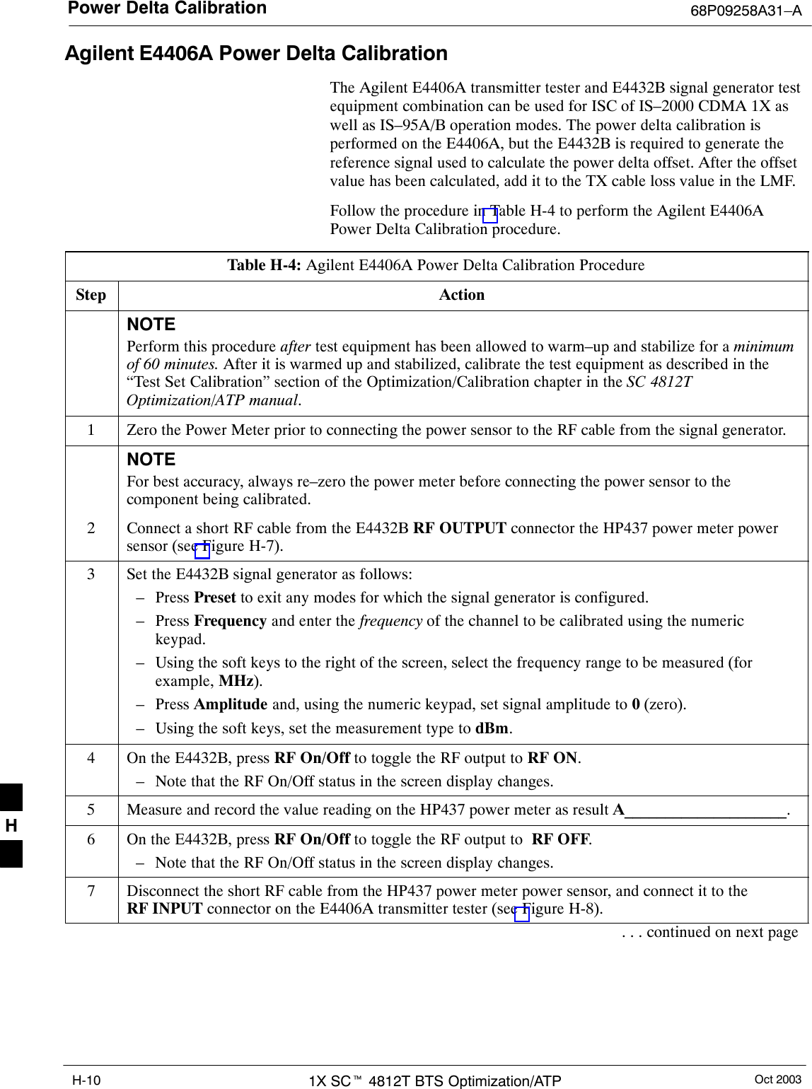
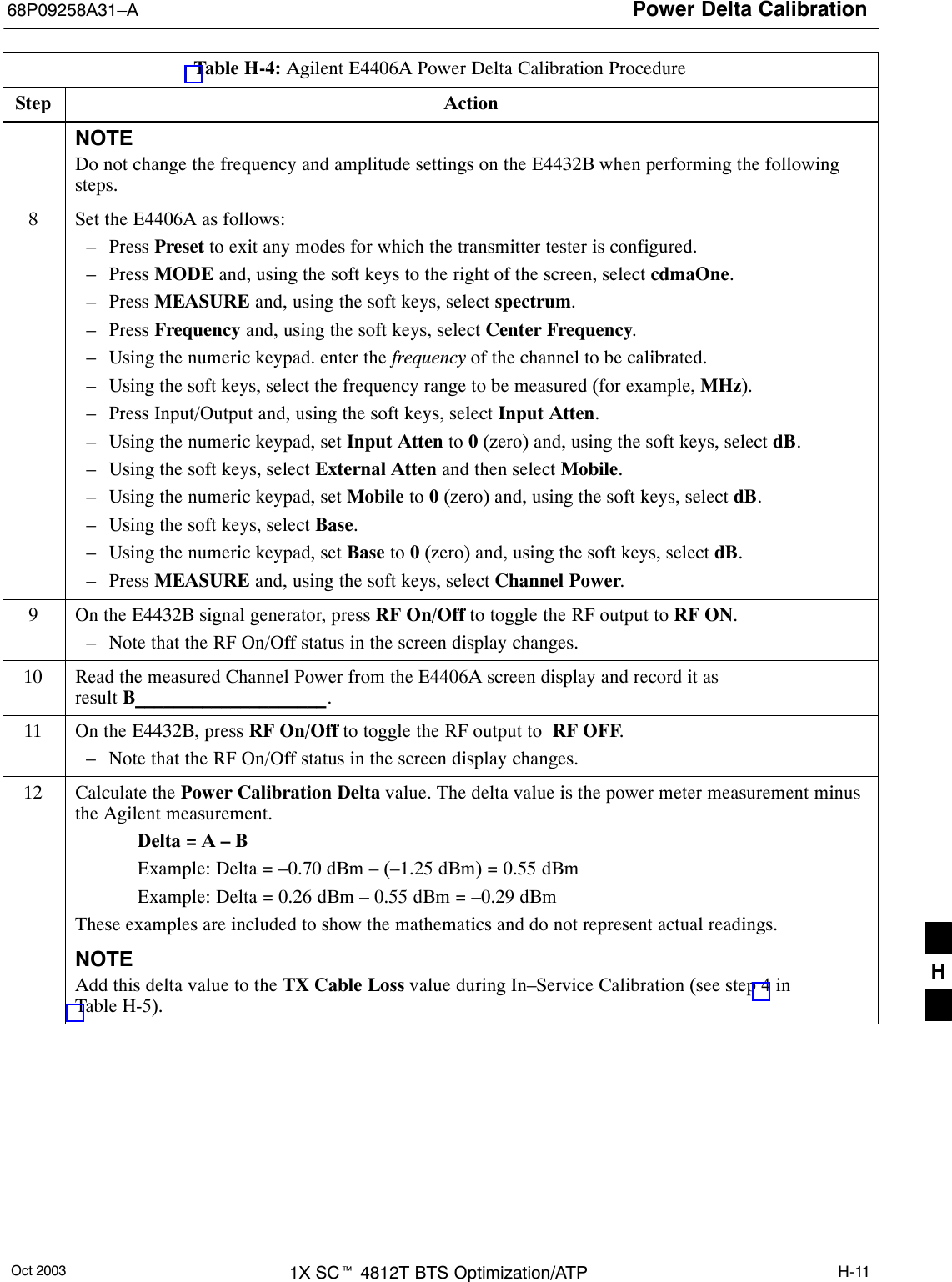
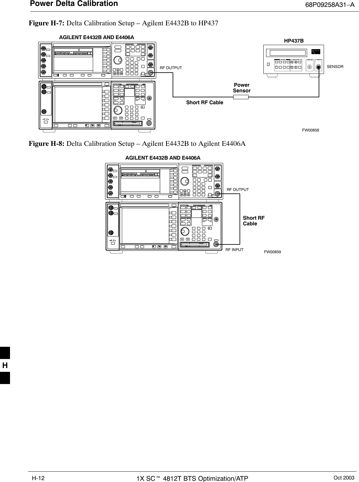
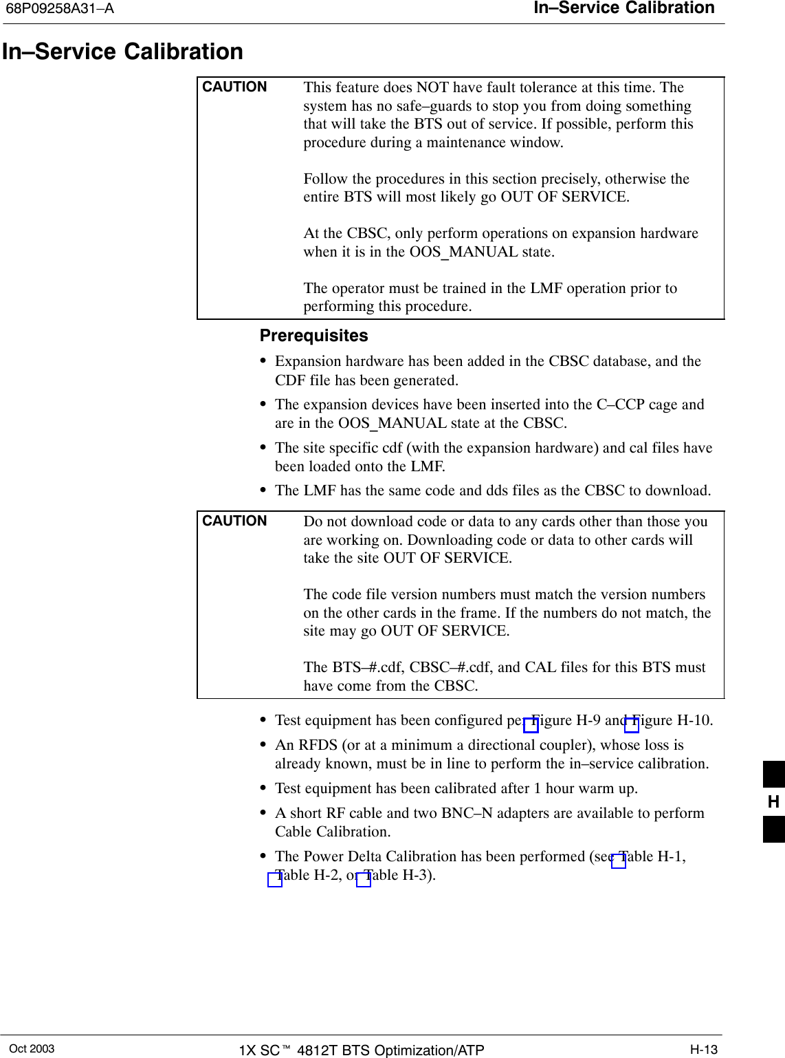
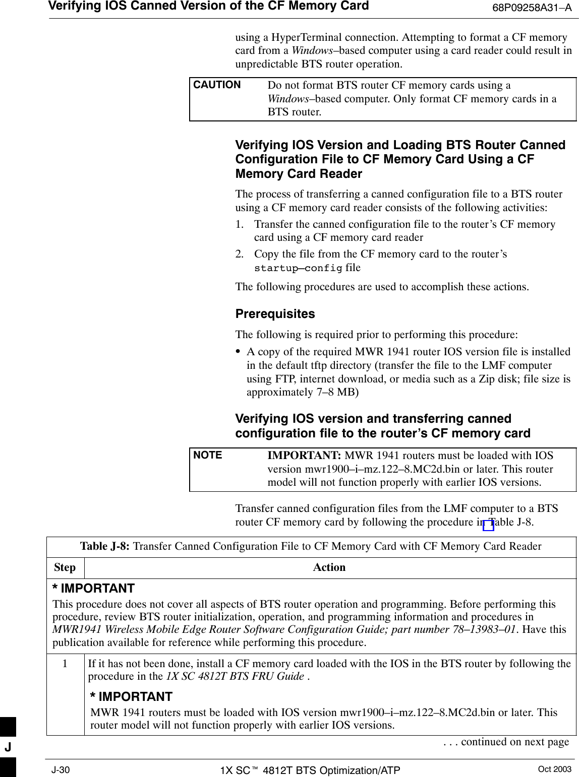
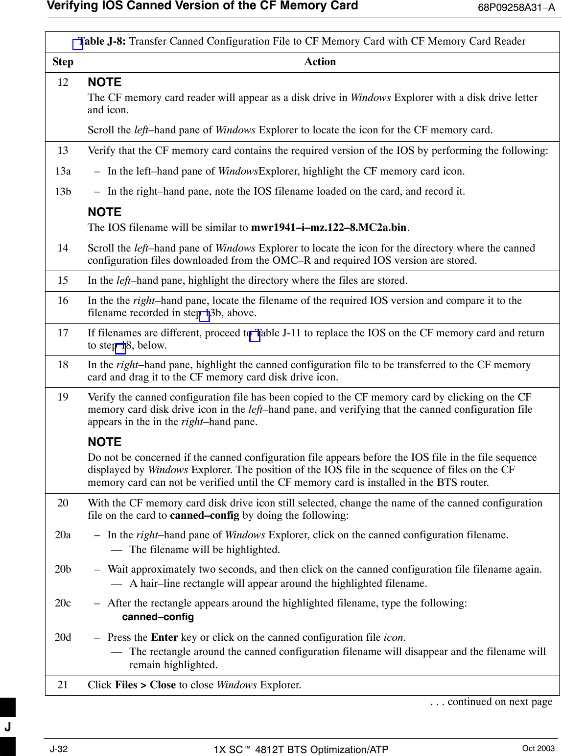
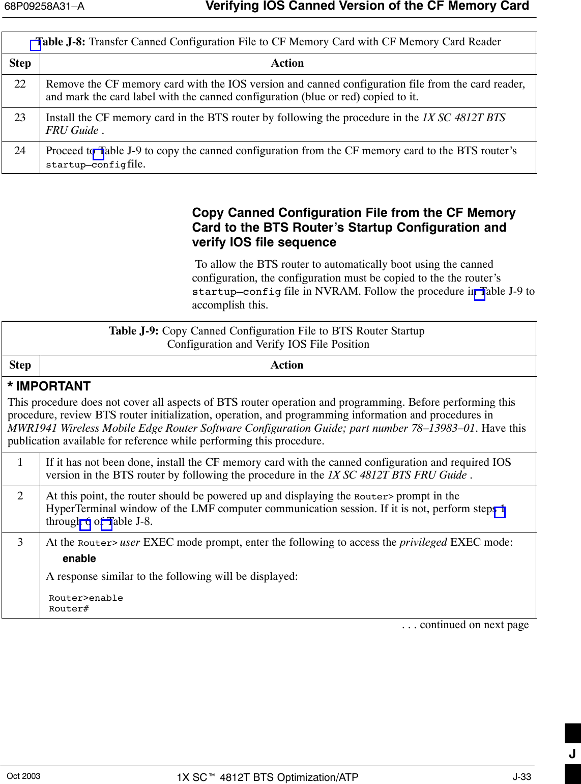
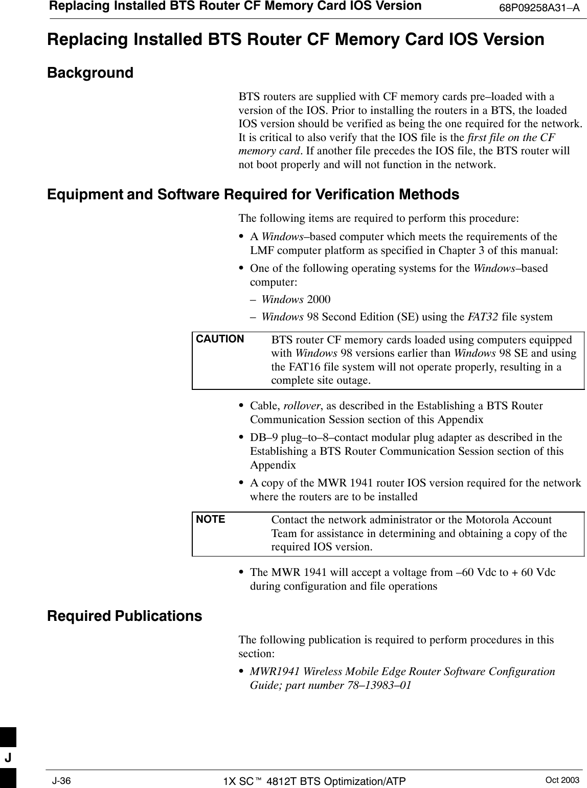
Nokia Solutions and Networks T6EF1 CDMA Base station transmitter User Manual 1X SC4812T BTS Optimization ATP Release 2 16 3 x

Nokia Solutions and Networks CDMA Base station transmitter 1X SC4812T BTS Optimization ATP Release 2 16 3 x

Contents

Users Manual 3

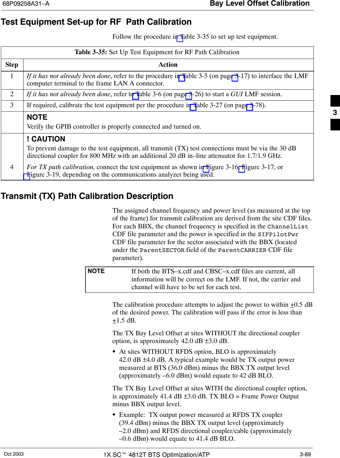
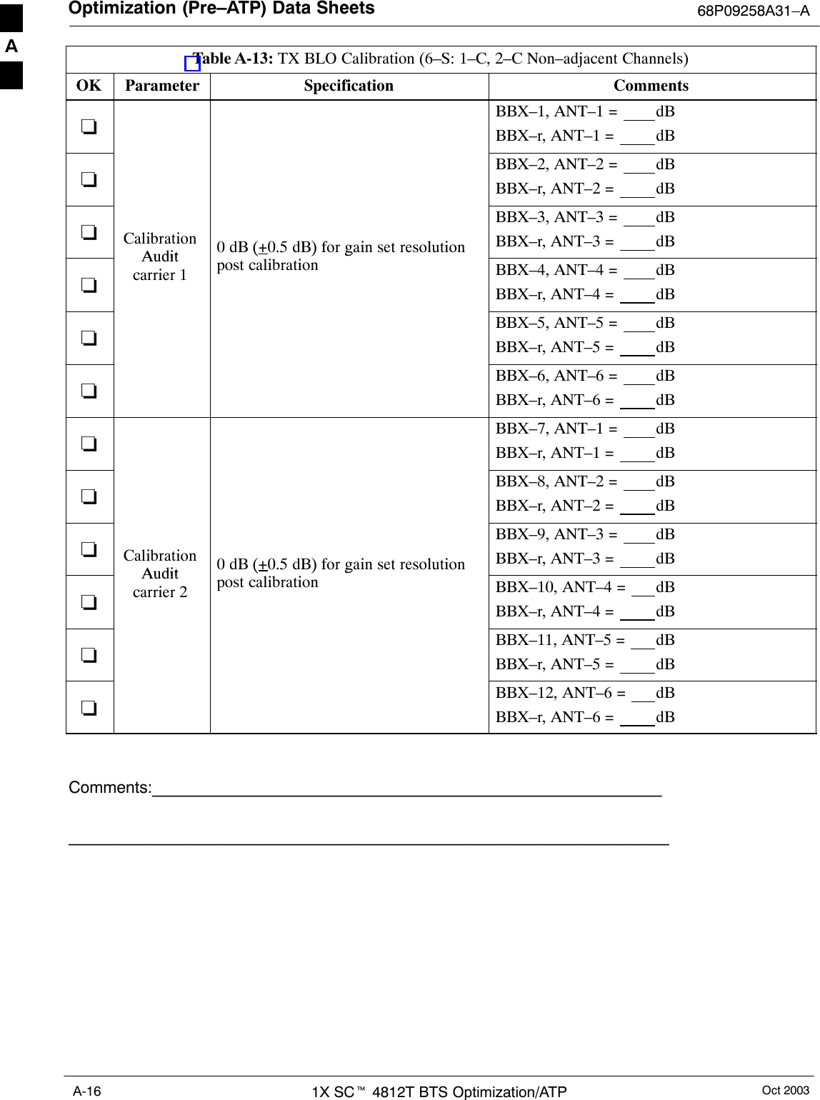
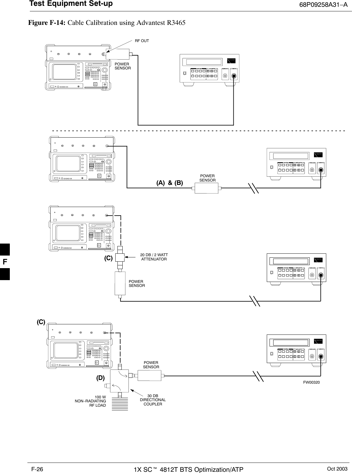
Bay Level Offset Calibration68P09258A31–AOct 2003 1X SCt 4812T BTS Optimization/ATP 3-89Test Equipment Set-up for RF Path CalibrationFollow the procedure in Table 3-35 to set up test equipment.Table 3-35: Set Up Test Equipment for RF Path CalibrationStep Action1If it has not already been done, refer to the procedure in Table 3-5 (on page 3-17) to interface the LMFcomputer terminal to the frame LAN A connector.2If it has not already been done, refer to Table 3-6 (on page 3-26) to start a GUI LMF session.3If required, calibrate the test equipment per the procedure in Table 3-27 (on page 3-78).NOTEVerify the GPIB controller is properly connected and turned on.! CAUTIONTo prevent damage to the test equipment, all transmit (TX) test connections must be via the 30 dBdirectional coupler for 800 MHz with an additional 20 dB in–line attenuator for 1.7/1.9 GHz.4For TX path calibration, connect the test equipment as shown in Figure 3-16, Figure 3-17, orFigure 3-19, depending on the communications analyzer being used.Transmit (TX) Path Calibration DescriptionThe assigned channel frequency and power level (as measured at the topof the frame) for transmit calibration are derived from the site CDF files.For each BBX, the channel frequency is specified in the ChannelListCDF file parameter and the power is specified in the SIFPilotPwrCDF file parameter for the sector associated with the BBX (locatedunder the ParentSECTOR field of the ParentCARRIER CDF fileparameter).NOTE If both the BTS–x.cdf and CBSC–x.cdf files are current, allinformation will be correct on the LMF. If not, the carrier andchannel will have to be set for each test.The calibration procedure attempts to adjust the power to within +0.5 dBof the desired power. The calibration will pass if the error is less than+1.5 dB.The TX Bay Level Offset at sites WITHOUT the directional coupleroption, is approximately 42.0 dB ±3.0 dB.SAt sites WITHOUT RFDS option, BLO is approximately 42.0 dB ±4.0 dB. A typical example would be TX output powermeasured at BTS (36.0 dBm) minus the BBX TX output level(approximately –6.0 dBm) would equate to 42 dB BLO.The TX Bay Level Offset at sites WITH the directional coupler option,is approximately 41.4 dB ±3.0 dB. TX BLO = Frame Power Outputminus BBX output level.SExample: TX output power measured at RFDS TX coupler(39.4 dBm) minus the BBX TX output level (approximately–2.0 dBm) and RFDS directional coupler/cable (approximately–0.6 dBm) would equate to 41.4 dB BLO.3
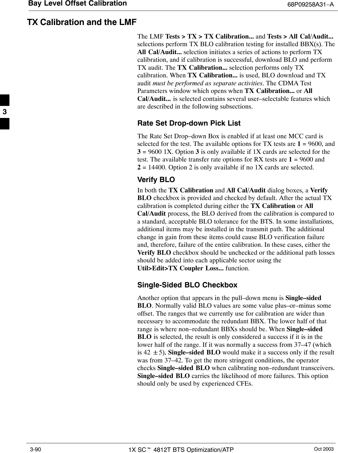
Bay Level Offset Calibration 68P09258A31–AOct 20031X SCt 4812T BTS Optimization/ATP3-90TX Calibration and the LMFThe LMF Tests > TX > TX Calibration... and Tests > All Cal/Audit...selections perform TX BLO calibration testing for installed BBX(s). TheAll Cal/Audit... selection initiates a series of actions to perform TXcalibration, and if calibration is successful, download BLO and performTX audit. The TX Calibration... selection performs only TXcalibration. When TX Calibration... is used, BLO download and TXaudit must be performed as separate activities. The CDMA TestParameters window which opens when TX Calibration... or AllCal/Audit... is selected contains several user–selectable features whichare described in the following subsections.Rate Set Drop-down Pick ListThe Rate Set Drop–down Box is enabled if at least one MCC card isselected for the test. The available options for TX tests are 1 = 9600, and3 = 9600 1X. Option 3 is only available if 1X cards are selected for thetest. The available transfer rate options for RX tests are 1 = 9600 and2 = 14400. Option 2 is only available if no 1X cards are selected.Verify BLOIn both the TX Calibration and All Cal/Audit dialog boxes, a VerifyBLO checkbox is provided and checked by default. After the actual TXcalibration is completed during either the TX Calibration or AllCal/Audit process, the BLO derived from the calibration is compared toa standard, acceptable BLO tolerance for the BTS. In some installations,additional items may be installed in the transmit path. The additionalchange in gain from these items could cause BLO verification failureand, therefore, failure of the entire calibration. In these cases, either theVerify BLO checkbox should be unchecked or the additional path lossesshould be added into each applicable sector using theUtil>Edit>TX Coupler Loss... function.Single-Sided BLO CheckboxAnother option that appears in the pull–down menu is Single–sidedBLO. Normally valid BLO values are some value plus–or–minus someoffset. The ranges that we currently use for calibration are wider thannecessary to accommodate the redundant BBX. The lower half of thatrange is where non–redundant BBXs should be. When Single–sidedBLO is selected, the result is only considered a success if it is in thelower half of the range. If it was normally a success from 37–47 (whichis 42 "5), Single–sided BLO would make it a success only if the resultwas from 37–42. To get the more stringent conditions, the operatorchecks Single–sided BLO when calibrating non–redundant transceivers.Single–sided BLO carries the likelihood of more failures. This optionshould only be used by experienced CFEs.3
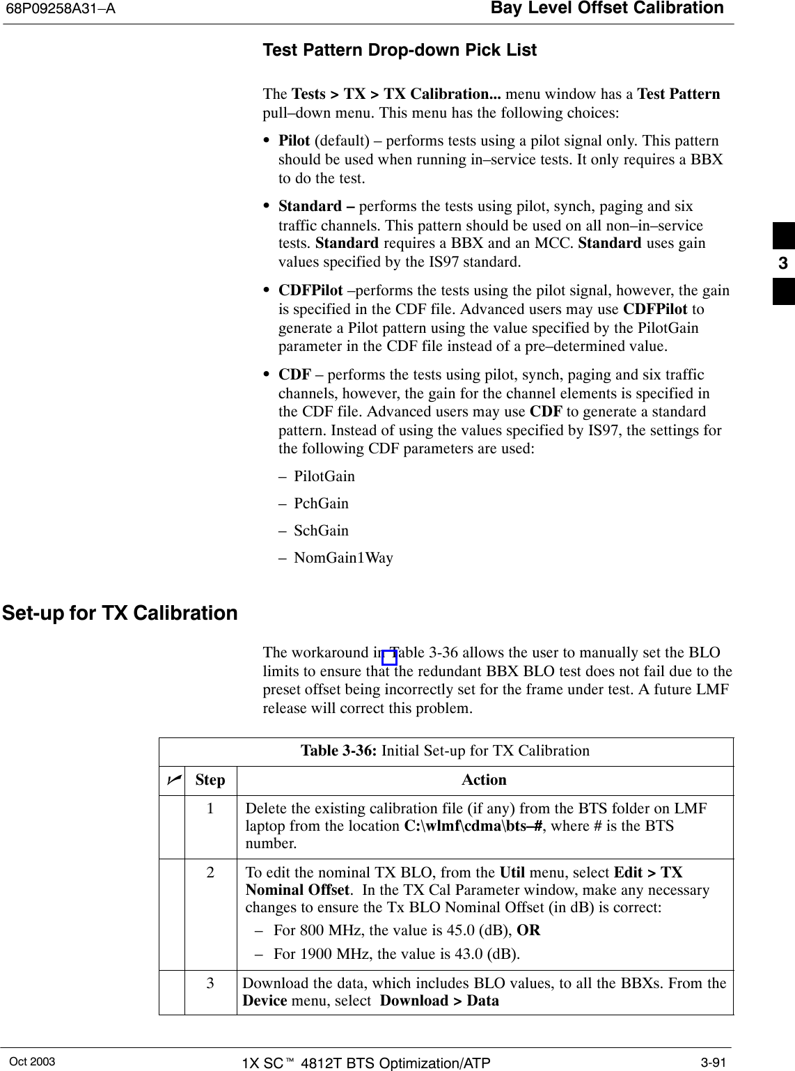
Bay Level Offset Calibration68P09258A31–AOct 2003 1X SCt 4812T BTS Optimization/ATP 3-91Test Pattern Drop-down Pick ListThe Tests > TX > TX Calibration... menu window has a Test Patternpull–down menu. This menu has the following choices:SPilot (default) – performs tests using a pilot signal only. This patternshould be used when running in–service tests. It only requires a BBXto do the test.SStandard – performs the tests using pilot, synch, paging and sixtraffic channels. This pattern should be used on all non–in–servicetests. Standard requires a BBX and an MCC. Standard uses gainvalues specified by the IS97 standard.SCDFPilot –performs the tests using the pilot signal, however, the gainis specified in the CDF file. Advanced users may use CDFPilot togenerate a Pilot pattern using the value specified by the PilotGainparameter in the CDF file instead of a pre–determined value.SCDF – performs the tests using pilot, synch, paging and six trafficchannels, however, the gain for the channel elements is specified inthe CDF file. Advanced users may use CDF to generate a standardpattern. Instead of using the values specified by IS97, the settings forthe following CDF parameters are used:– PilotGain– PchGain– SchGain– NomGain1WaySet-up for TX CalibrationThe workaround in Table 3-36 allows the user to manually set the BLOlimits to ensure that the redundant BBX BLO test does not fail due to thepreset offset being incorrectly set for the frame under test. A future LMFrelease will correct this problem.Table 3-36: Initial Set-up for TX CalibrationnStep Action1Delete the existing calibration file (if any) from the BTS folder on LMFlaptop from the location C:\wlmf\cdma\bts–#, where # is the BTSnumber.2To edit the nominal TX BLO, from the Util menu, select Edit > TXNominal Offset.  In the TX Cal Parameter window, make any necessarychanges to ensure the Tx BLO Nominal Offset (in dB) is correct:– For 800 MHz, the value is 45.0 (dB), OR– For 1900 MHz, the value is 43.0 (dB).3Download the data, which includes BLO values, to all the BBXs. From theDevice menu, select  Download > Data 3
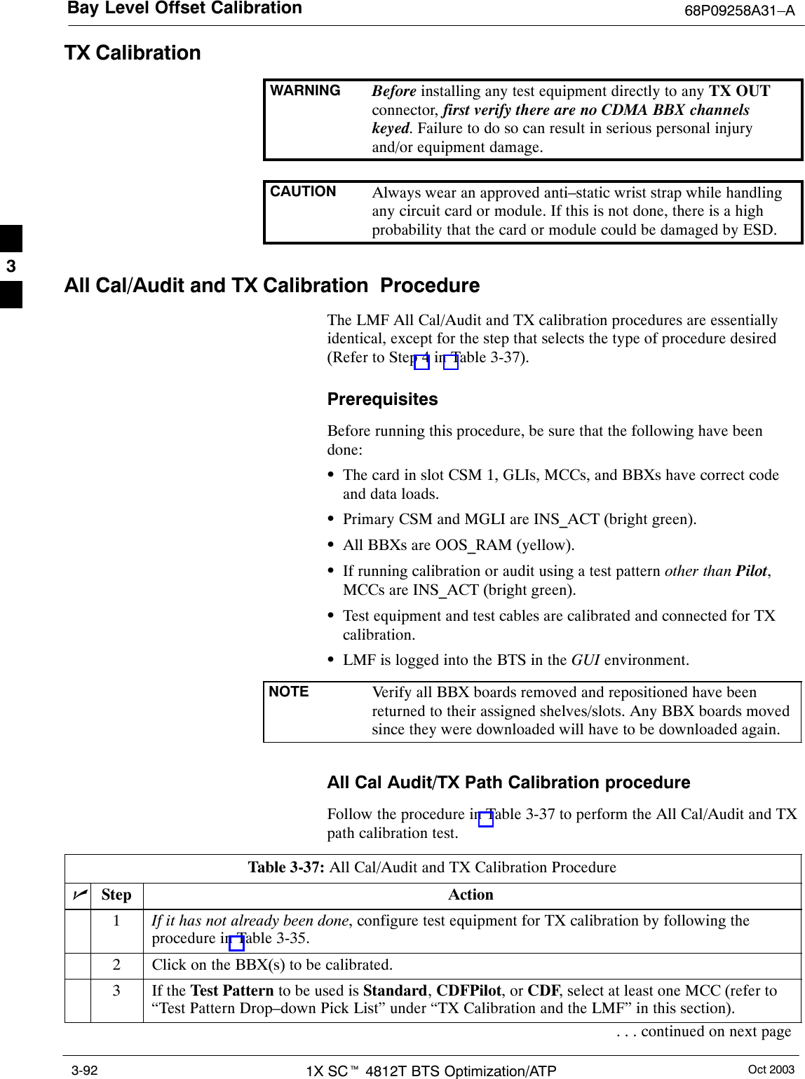
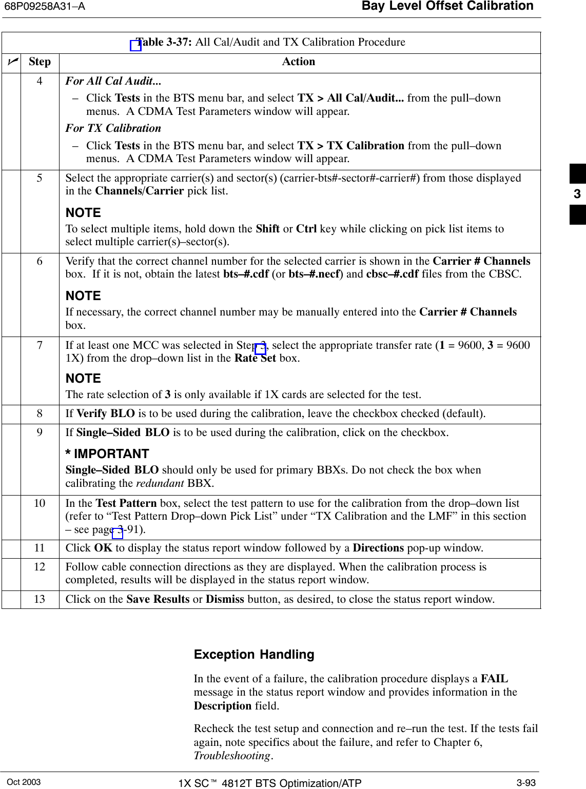
Bay Level Offset Calibration 68P09258A31–AOct 20031X SCt 4812T BTS Optimization/ATP3-92TX CalibrationWARNING Before installing any test equipment directly to any TX OUTconnector, first verify there are no CDMA BBX channelskeyed. Failure to do so can result in serious personal injuryand/or equipment damage.CAUTION Always wear an approved anti–static wrist strap while handlingany circuit card or module. If this is not done, there is a highprobability that the card or module could be damaged by ESD.All Cal/Audit and TX Calibration  ProcedureThe LMF All Cal/Audit and TX calibration procedures are essentiallyidentical, except for the step that selects the type of procedure desired(Refer to Step 4 in Table 3-37).PrerequisitesBefore running this procedure, be sure that the following have beendone:SThe card in slot CSM 1, GLIs, MCCs, and BBXs have correct codeand data loads.SPrimary CSM and MGLI are INS_ACT (bright green).SAll BBXs are OOS_RAM (yellow).SIf running calibration or audit using a test pattern other than Pilot,MCCs are INS_ACT (bright green).STest equipment and test cables are calibrated and connected for TXcalibration.SLMF is logged into the BTS in the GUI environment.NOTE Verify all BBX boards removed and repositioned have beenreturned to their assigned shelves/slots. Any BBX boards movedsince they were downloaded will have to be downloaded again.All Cal Audit/TX Path Calibration procedureFollow the procedure in Table 3-37 to perform the All Cal/Audit and TXpath calibration test.Table 3-37: All Cal/Audit and TX Calibration ProcedurenStep Action1If it has not already been done, configure test equipment for TX calibration by following theprocedure in Table 3-35.2Click on the BBX(s) to be calibrated.3If the Test Pattern to be used is Standard, CDFPilot, or CDF, select at least one MCC (refer to“Test Pattern Drop–down Pick List” under “TX Calibration and the LMF” in this section).. . . continued on next page3
Bay Level Offset Calibration68P09258A31–AOct 2003 1X SCt 4812T BTS Optimization/ATP 3-93Table 3-37: All Cal/Audit and TX Calibration ProcedurenActionStep4For All Cal Audit...– Click Tests in the BTS menu bar, and select TX > All Cal/Audit... from the pull–downmenus.  A CDMA Test Parameters window will appear.For TX Calibration– Click Tests in the BTS menu bar, and select TX > TX Calibration from the pull–downmenus.  A CDMA Test Parameters window will appear.5Select the appropriate carrier(s) and sector(s) (carrier-bts#-sector#-carrier#) from those displayedin the Channels/Carrier pick list.NOTETo select multiple items, hold down the Shift or Ctrl key while clicking on pick list items toselect multiple carrier(s)–sector(s).6Verify that the correct channel number for the selected carrier is shown in the Carrier # Channelsbox.  If it is not, obtain the latest bts–#.cdf (or bts–#.necf) and cbsc–#.cdf files from the CBSC.NOTEIf necessary, the correct channel number may be manually entered into the Carrier # Channelsbox.7If at least one MCC was selected in Step 3, select the appropriate transfer rate (1 = 9600, 3 = 96001X) from the drop–down list in the Rate Set box.NOTEThe rate selection of 3 is only available if 1X cards are selected for the test.8 If Verify BLO is to be used during the calibration, leave the checkbox checked (default).9If Single–Sided BLO is to be used during the calibration, click on the checkbox.* IMPORTANTSingle–Sided BLO should only be used for primary BBXs. Do not check the box whencalibrating the redundant BBX.10 In the Test Pattern box, select the test pattern to use for the calibration from the drop–down list(refer to “Test Pattern Drop–down Pick List” under “TX Calibration and the LMF” in this section– see page 3-91).11 Click OK to display the status report window followed by a Directions pop-up window.12 Follow cable connection directions as they are displayed. When the calibration process iscompleted, results will be displayed in the status report window.13 Click on the Save Results or Dismiss button, as desired, to close the status report window. Exception HandlingIn the event of a failure, the calibration procedure displays a FAILmessage in the status report window and provides information in theDescription field.Recheck the test setup and connection and re–run the test. If the tests failagain, note specifics about the failure, and refer to Chapter 6,Troubleshooting.3
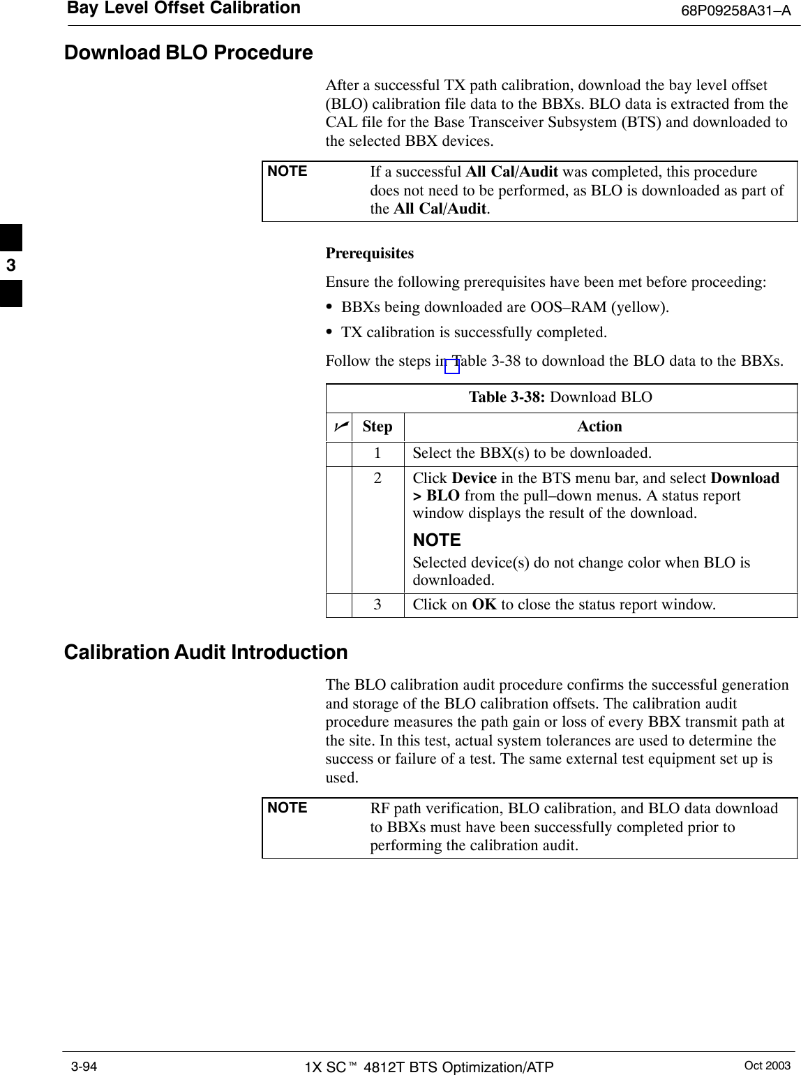
Bay Level Offset Calibration 68P09258A31–AOct 20031X SCt 4812T BTS Optimization/ATP3-94Download BLO ProcedureAfter a successful TX path calibration, download the bay level offset(BLO) calibration file data to the BBXs. BLO data is extracted from theCAL file for the Base Transceiver Subsystem (BTS) and downloaded tothe selected BBX devices.NOTE If a successful All Cal/Audit was completed, this proceduredoes not need to be performed, as BLO is downloaded as part ofthe All Cal/Audit.PrerequisitesEnsure the following prerequisites have been met before proceeding:SBBXs being downloaded are OOS–RAM (yellow).STX calibration is successfully completed.Follow the steps in Table 3-38 to download the BLO data to the BBXs.Table 3-38: Download BLOnStep Action1Select the BBX(s) to be downloaded.2 Click Device in the BTS menu bar, and select Download> BLO from the pull–down menus. A status reportwindow displays the result of the download.NOTESelected device(s) do not change color when BLO isdownloaded.3Click on OK to close the status report window.Calibration Audit IntroductionThe BLO calibration audit procedure confirms the successful generationand storage of the BLO calibration offsets. The calibration auditprocedure measures the path gain or loss of every BBX transmit path atthe site. In this test, actual system tolerances are used to determine thesuccess or failure of a test. The same external test equipment set up isused.NOTE RF path verification, BLO calibration, and BLO data downloadto BBXs must have been successfully completed prior toperforming the calibration audit.3
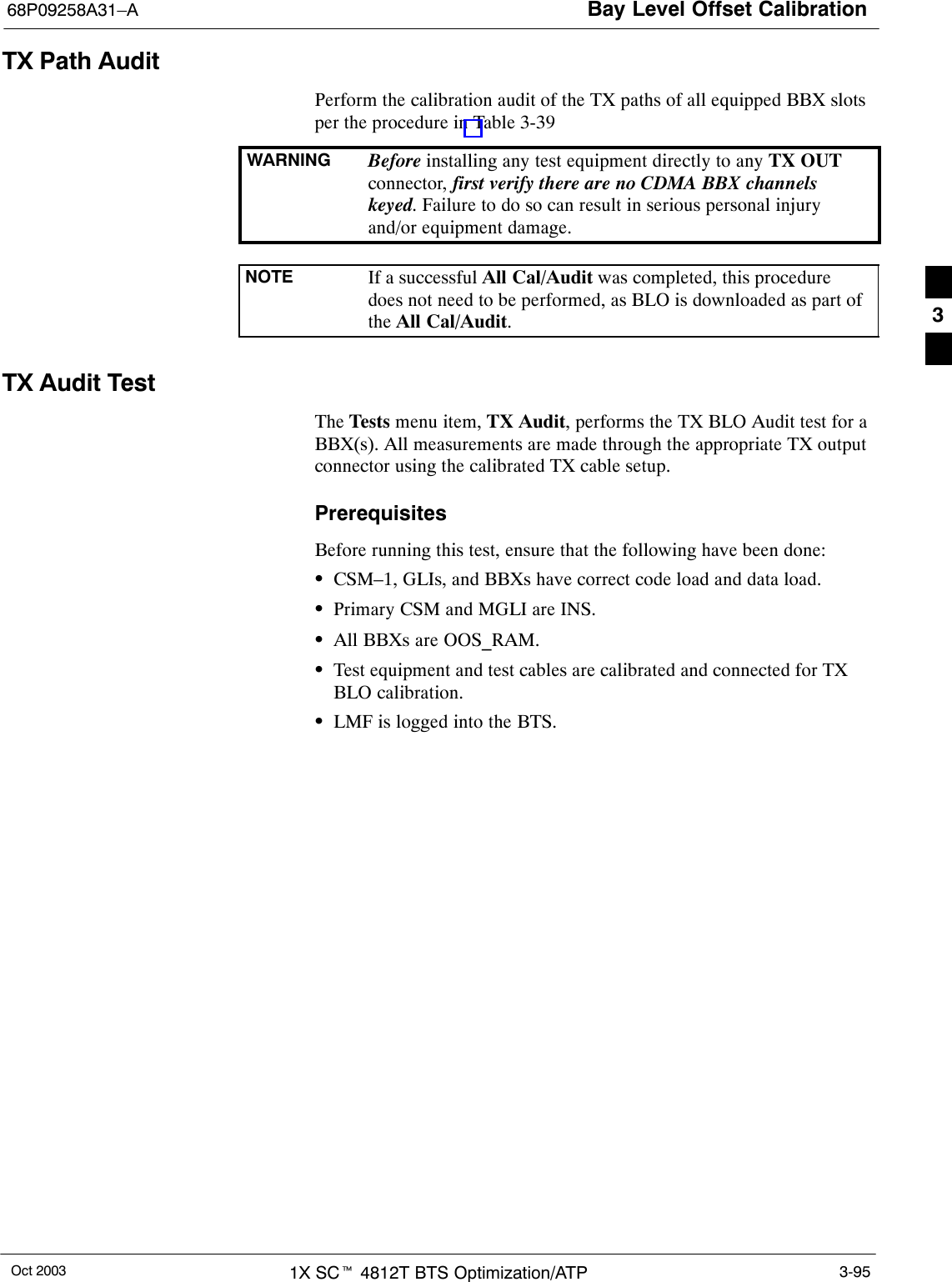
Bay Level Offset Calibration68P09258A31–AOct 2003 1X SCt 4812T BTS Optimization/ATP 3-95TX Path AuditPerform the calibration audit of the TX paths of all equipped BBX slotsper the procedure in Table 3-39WARNING Before installing any test equipment directly to any TX OUTconnector, first verify there are no CDMA BBX channelskeyed. Failure to do so can result in serious personal injuryand/or equipment damage.NOTE If a successful All Cal/Audit was completed, this proceduredoes not need to be performed, as BLO is downloaded as part ofthe All Cal/Audit.TX Audit TestThe Tests menu item, TX Audit, performs the TX BLO Audit test for aBBX(s). All measurements are made through the appropriate TX outputconnector using the calibrated TX cable setup.PrerequisitesBefore running this test, ensure that the following have been done:SCSM–1, GLIs, and BBXs have correct code load and data load.SPrimary CSM and MGLI are INS.SAll BBXs are OOS_RAM.STest equipment and test cables are calibrated and connected for TXBLO calibration.SLMF is logged into the BTS.3
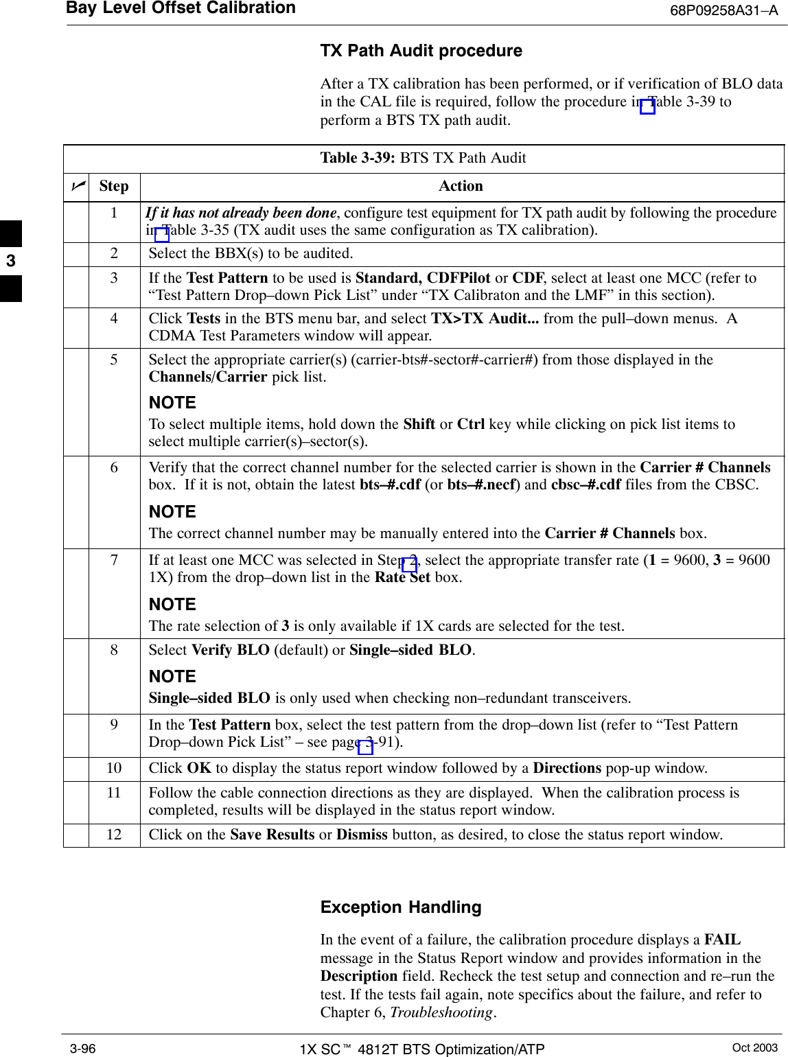
Bay Level Offset Calibration 68P09258A31–AOct 20031X SCt 4812T BTS Optimization/ATP3-96TX Path Audit procedureAfter a TX calibration has been performed, or if verification of BLO datain the CAL file is required, follow the procedure in Table 3-39 toperform a BTS TX path audit.Table 3-39: BTS TX Path AuditnStep Action1If it has not already been done, configure test equipment for TX path audit by following the procedurein Table 3-35 (TX audit uses the same configuration as TX calibration).2Select the BBX(s) to be audited.3If the Test Pattern to be used is Standard, CDFPilot or CDF, select at least one MCC (refer to“Test Pattern Drop–down Pick List” under “TX Calibraton and the LMF” in this section).4 Click Tests in the BTS menu bar, and select TX>TX Audit... from the pull–down menus.  ACDMA Test Parameters window will appear.5Select the appropriate carrier(s) (carrier-bts#-sector#-carrier#) from those displayed in theChannels/Carrier pick list.NOTETo select multiple items, hold down the Shift or Ctrl key while clicking on pick list items toselect multiple carrier(s)–sector(s).6Verify that the correct channel number for the selected carrier is shown in the Carrier # Channelsbox.  If it is not, obtain the latest bts–#.cdf (or bts–#.necf) and cbsc–#.cdf files from the CBSC.NOTEThe correct channel number may be manually entered into the Carrier # Channels box.7If at least one MCC was selected in Step 2, select the appropriate transfer rate (1 = 9600, 3 = 96001X) from the drop–down list in the Rate Set box.NOTEThe rate selection of 3 is only available if 1X cards are selected for the test.8 Select Verify BLO (default) or Single–sided BLO.NOTESingle–sided BLO is only used when checking non–redundant transceivers.9In the Test Pattern box, select the test pattern from the drop–down list (refer to “Test PatternDrop–down Pick List” – see page 3-91).10 Click OK to display the status report window followed by a Directions pop-up window.11 Follow the cable connection directions as they are displayed.  When the calibration process iscompleted, results will be displayed in the status report window.12 Click on the Save Results or Dismiss button, as desired, to close the status report window. Exception HandlingIn the event of a failure, the calibration procedure displays a FAILmessage in the Status Report window and provides information in theDescription field. Recheck the test setup and connection and re–run thetest. If the tests fail again, note specifics about the failure, and refer toChapter 6, Troubleshooting.3
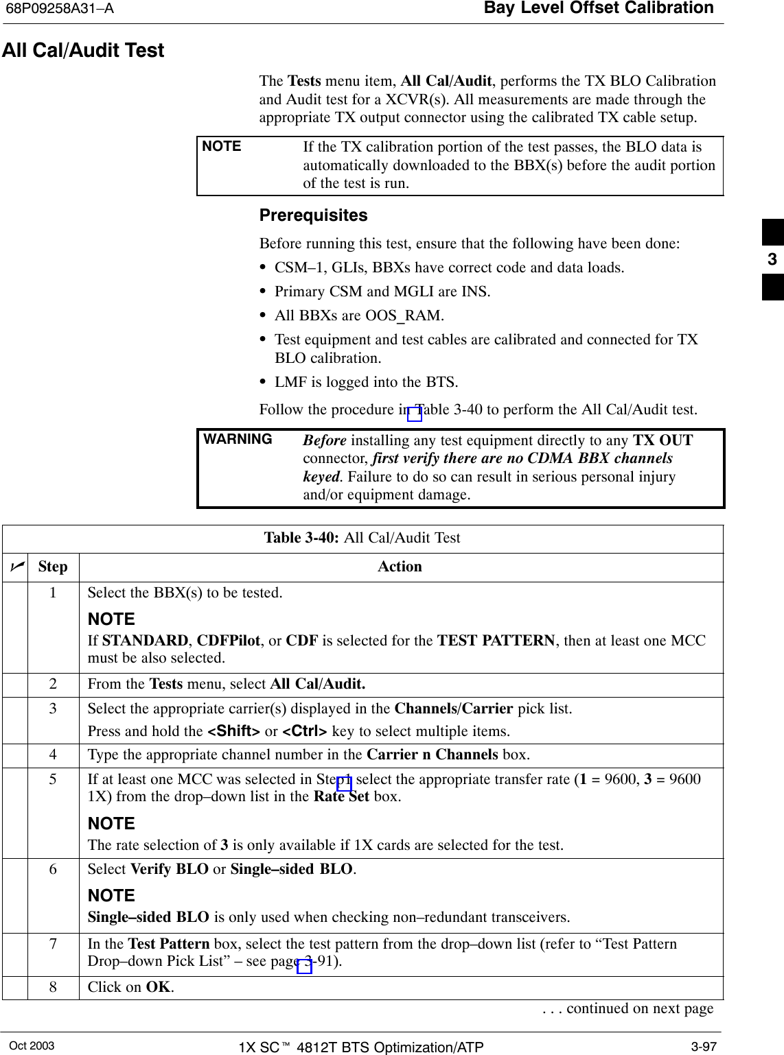
Bay Level Offset Calibration68P09258A31–AOct 2003 1X SCt 4812T BTS Optimization/ATP 3-97All Cal/Audit TestThe Tests menu item, All Cal/Audit, performs the TX BLO Calibrationand Audit test for a XCVR(s). All measurements are made through theappropriate TX output connector using the calibrated TX cable setup.NOTE If the TX calibration portion of the test passes, the BLO data isautomatically downloaded to the BBX(s) before the audit portionof the test is run.PrerequisitesBefore running this test, ensure that the following have been done:SCSM–1, GLIs, BBXs have correct code and data loads.SPrimary CSM and MGLI are INS.SAll BBXs are OOS_RAM.STest equipment and test cables are calibrated and connected for TXBLO calibration.SLMF is logged into the BTS.Follow the procedure in Table 3-40 to perform the All Cal/Audit test.WARNING Before installing any test equipment directly to any TX OUTconnector, first verify there are no CDMA BBX channelskeyed. Failure to do so can result in serious personal injuryand/or equipment damage.Table 3-40: All Cal/Audit TestnStep Action1Select the BBX(s) to be tested.NOTEIf STANDARD, CDFPilot, or CDF is selected for the TEST PATTERN, then at least one MCCmust be also selected.2From the Tests menu, select All Cal/Audit.3Select the appropriate carrier(s) displayed in the Channels/Carrier pick list.Press and hold the <Shift> or <Ctrl> key to select multiple items.4Type the appropriate channel number in the Carrier n Channels box.5If at least one MCC was selected in Step1 select the appropriate transfer rate (1 = 9600, 3 = 96001X) from the drop–down list in the Rate Set box.NOTEThe rate selection of 3 is only available if 1X cards are selected for the test.6 Select Verify BLO or Single–sided BLO.NOTESingle–sided BLO is only used when checking non–redundant transceivers.7In the Test Pattern box, select the test pattern from the drop–down list (refer to “Test PatternDrop–down Pick List” – see page 3-91).8Click on OK.. . . continued on next page3
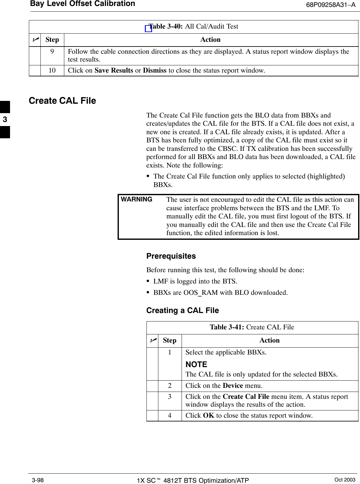
Bay Level Offset Calibration 68P09258A31–AOct 20031X SCt 4812T BTS Optimization/ATP3-98Table 3-40: All Cal/Audit TestnActionStep9Follow the cable connection directions as they are displayed. A status report window displays thetest results.10 Click on Save Results or Dismiss to close the status report window. Create CAL FileThe Create Cal File function gets the BLO data from BBXs andcreates/updates the CAL file for the BTS. If a CAL file does not exist, anew one is created. If a CAL file already exists, it is updated. After aBTS has been fully optimized, a copy of the CAL file must exist so itcan be transferred to the CBSC. If TX calibration has been successfullyperformed for all BBXs and BLO data has been downloaded, a CAL fileexists. Note the following:SThe Create Cal File function only applies to selected (highlighted)BBXs.WARNING The user is not encouraged to edit the CAL file as this action cancause interface problems between the BTS and the LMF. Tomanually edit the CAL file, you must first logout of the BTS. Ifyou manually edit the CAL file and then use the Create Cal Filefunction, the edited information is lost.PrerequisitesBefore running this test, the following should be done:SLMF is logged into the BTS.SBBXs are OOS_RAM with BLO downloaded.Creating a CAL FileTable 3-41: Create CAL FilenStep Action1Select the applicable BBXs.NOTEThe CAL file is only updated for the selected BBXs.2Click on the Device menu.3Click on the Create Cal File menu item. A status reportwindow displays the results of the action.4 Click OK to close the status report window. 3
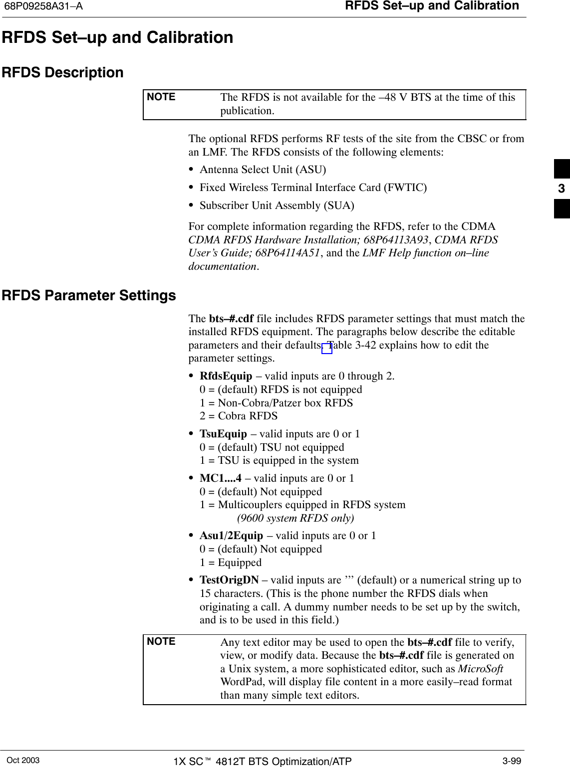
RFDS Set–up and Calibration68P09258A31–AOct 2003 1X SCt 4812T BTS Optimization/ATP 3-99RFDS Set–up and CalibrationRFDS DescriptionNOTE The RFDS is not available for the –48 V BTS at the time of thispublication.The optional RFDS performs RF tests of the site from the CBSC or froman LMF. The RFDS consists of the following elements:SAntenna Select Unit (ASU)SFixed Wireless Terminal Interface Card (FWTIC)SSubscriber Unit Assembly (SUA)For complete information regarding the RFDS, refer to the CDMACDMA RFDS Hardware Installation; 68P64113A93, CDMA RFDSUser’s Guide; 68P64114A51, and the LMF Help function on–linedocumentation.RFDS Parameter SettingsThe bts–#.cdf file includes RFDS parameter settings that must match theinstalled RFDS equipment. The paragraphs below describe the editableparameters and their defaults. Table 3-42 explains how to edit theparameter settings.SRfdsEquip – valid inputs are 0 through 2.0 = (default) RFDS is not equipped1 = Non-Cobra/Patzer box RFDS2 = Cobra RFDSSTsuEquip – valid inputs are 0 or 10 = (default) TSU not equipped1 = TSU is equipped in the systemSMC1....4 – valid inputs are 0 or 10 = (default) Not equipped1 = Multicouplers equipped in RFDS system (9600 system RFDS only)SAsu1/2Equip – valid inputs are 0 or 10 = (default) Not equipped1 = EquippedSTestOrigDN – valid inputs are ’’’ (default) or a numerical string up to15 characters. (This is the phone number the RFDS dials whenoriginating a call. A dummy number needs to be set up by the switch,and is to be used in this field.)NOTE Any text editor may be used to open the bts–#.cdf file to verify,view, or modify data. Because the bts–#.cdf file is generated ona Unix system, a more sophisticated editor, such as MicroSoftWordPad, will display file content in a more easily–read formatthan many simple text editors.3
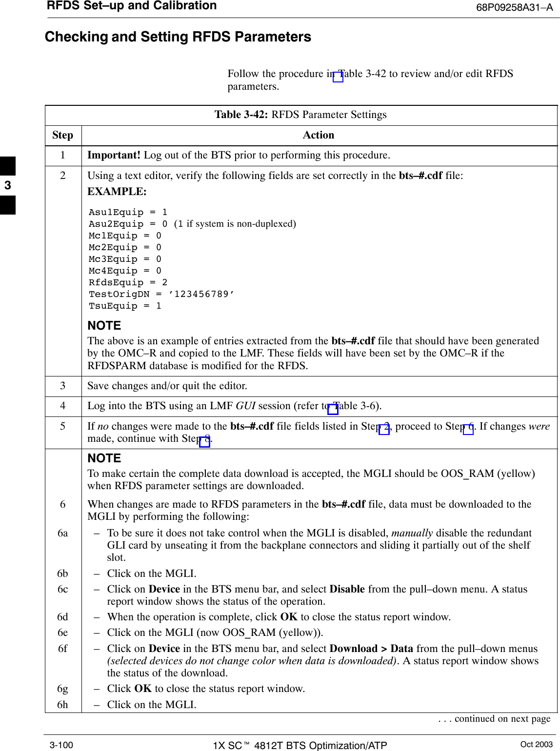
RFDS Set–up and Calibration 68P09258A31–AOct 20031X SCt 4812T BTS Optimization/ATP3-100Checking and Setting RFDS ParametersFollow the procedure in Table 3-42 to review and/or edit RFDSparameters.Table 3-42: RFDS Parameter SettingsStep Action1Important! Log out of the BTS prior to performing this procedure.2Using a text editor, verify the following fields are set correctly in the bts–#.cdf file:EXAMPLE:Asu1Equip = 1Asu2Equip = 0 (1 if system is non-duplexed)Mc1Equip = 0Mc2Equip = 0Mc3Equip = 0Mc4Equip = 0RfdsEquip = 2TestOrigDN = ’123456789’TsuEquip = 1NOTEThe above is an example of entries extracted from the bts–#.cdf file that should have been generatedby the OMC–R and copied to the LMF. These fields will have been set by the OMC–R if theRFDSPARM database is modified for the RFDS.3Save changes and/or quit the editor.4Log into the BTS using an LMF GUI session (refer to Table 3-6).5 If no changes were made to the bts–#.cdf file fields listed in Step 2, proceed to Step 6. If changes weremade, continue with Step 8.NOTETo make certain the complete data download is accepted, the MGLI should be OOS_RAM (yellow)when RFDS parameter settings are downloaded.6When changes are made to RFDS parameters in the bts–#.cdf file, data must be downloaded to theMGLI by performing the following:6a – To be sure it does not take control when the MGLI is disabled, manually disable the redundantGLI card by unseating it from the backplane connectors and sliding it partially out of the shelfslot.6b – Click on the MGLI.6c – Click on Device in the BTS menu bar, and select Disable from the pull–down menu. A statusreport window shows the status of the operation.6d – When the operation is complete, click OK to close the status report window.6e – Click on the MGLI (now OOS_RAM (yellow)).6f – Click on Device in the BTS menu bar, and select Download > Data from the pull–down menus(selected devices do not change color when data is downloaded). A status report window showsthe status of the download.6g – Click OK to close the status report window.6h – Click on the MGLI.. . . continued on next page3
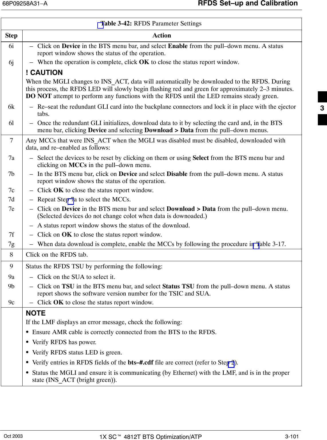
RFDS Set–up and Calibration68P09258A31–AOct 2003 1X SCt 4812T BTS Optimization/ATP 3-101Table 3-42: RFDS Parameter SettingsStep Action6i – Click on Device in the BTS menu bar, and select Enable from the pull–down menu. A statusreport window shows the status of the operation.6j – When the operation is complete, click OK to close the status report window.j! CAUTIONWhen the MGLI changes to INS_ACT, data will automatically be downloaded to the RFDS. Duringthis process, the RFDS LED will slowly begin flashing red and green for approximately 2–3 minutes.DO NOT attempt to perform any functions with the RFDS until the LED remains steady green.6k – Re–seat the redundant GLI card into the backplane connectors and lock it in place with the ejectortabs.6l – Once the redundant GLI initializes, download data to it by selecting the card and, in the BTSmenu bar, clicking Device and selecting Download > Data from the pull–down menus.7Any MCCs that were INS_ACT when the MGLI was disabled must be disabled, downloaded withdata, and re–enabled as follows:7a – Select the devices to be reset by clicking on them or using Select from the BTS menu bar andclicking on MCCs in the pull–down menu.7b – In the BTS menu bar, click on Device and select Disable from the pull–down menu. A statusreport window shows the status of the operation.7c – Click OK to close the status report window.7d – Repeat Step 7a to select the MCCs.7e – Click on Device in the BTS menu bar and select Download > Data from the pull–down menu.(Selected devices do not change colot when data is downoaded.)– A status report window shows the status of the download.7f – Click on OK to close the status report window.7g – When data download is complete, enable the MCCs by following the procedure in Table 3-17.8Click on the RFDS tab.9Status the RFDS TSU by performing the following:9a – Click on the SUA to select it.9b – Click on TSU in the BTS menu bar, and select Status TSU from the pull–down menu. A statusreport shows the software version number for the TSIC and SUA.9c – Click OK to close the status report window.NOTEIf the LMF displays an error message, check the following:SEnsure AMR cable is correctly connected from the BTS to the RFDS.SVerify RFDS has power.SVerify RFDS status LED is green.SVerify entries in RFDS fields of the bts–#.cdf file are correct (refer to Step 2).SStatus the MGLI and ensure it is communicating (by Ethernet) with the LMF, and is in the properstate (INS_ACT (bright green)). 3
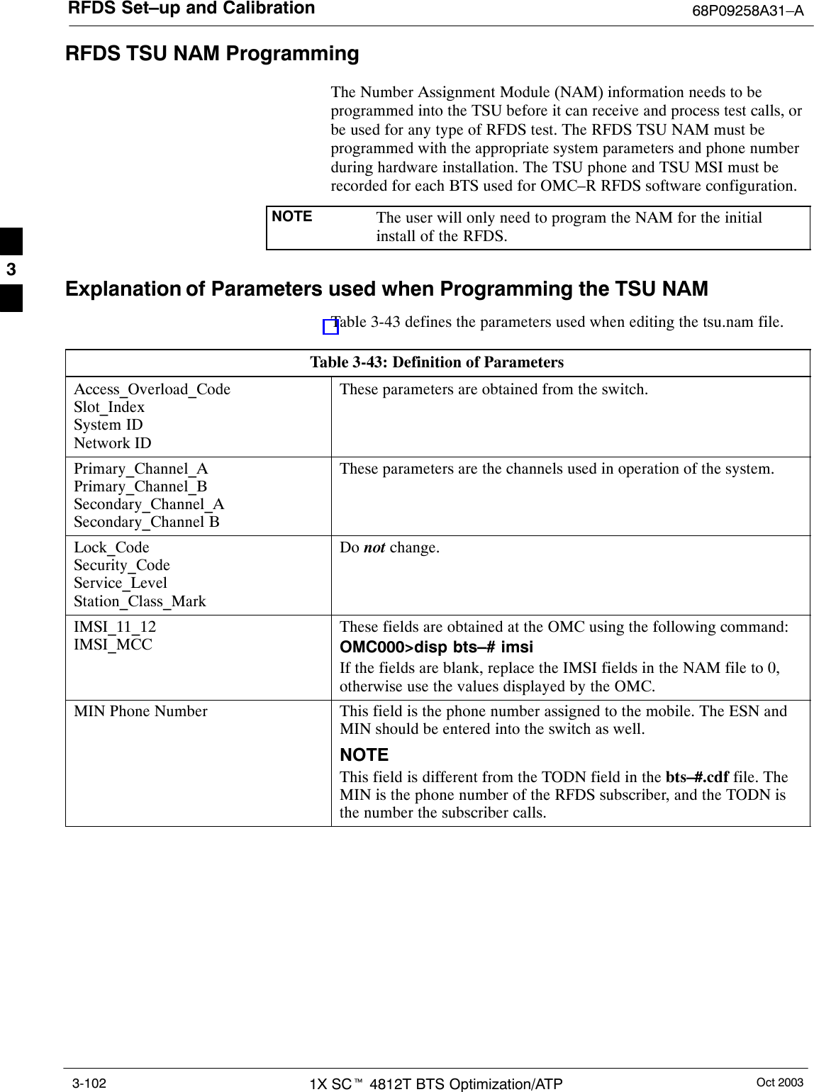
RFDS Set–up and Calibration 68P09258A31–AOct 20031X SCt 4812T BTS Optimization/ATP3-102RFDS TSU NAM ProgrammingThe Number Assignment Module (NAM) information needs to beprogrammed into the TSU before it can receive and process test calls, orbe used for any type of RFDS test. The RFDS TSU NAM must beprogrammed with the appropriate system parameters and phone numberduring hardware installation. The TSU phone and TSU MSI must berecorded for each BTS used for OMC–R RFDS software configuration.NOTE The user will only need to program the NAM for the initialinstall of the RFDS.Explanation of Parameters used when Programming the TSU NAMTable 3-43 defines the parameters used when editing the tsu.nam file.Table 3-43: Definition of ParametersAccess_Overload_CodeSlot_IndexSystem IDNetwork IDThese parameters are obtained from the switch.Primary_Channel_APrimary_Channel_BSecondary_Channel_ASecondary_Channel BThese parameters are the channels used in operation of the system.Lock_CodeSecurity_CodeService_LevelStation_Class_MarkDo not change.IMSI_11_12IMSI_MCCThese fields are obtained at the OMC using the following command:OMC000>disp bts–# imsiIf the fields are blank, replace the IMSI fields in the NAM file to 0,otherwise use the values displayed by the OMC.MIN Phone Number This field is the phone number assigned to the mobile. The ESN andMIN should be entered into the switch as well.NOTEThis field is different from the TODN field in the bts–#.cdf file. TheMIN is the phone number of the RFDS subscriber, and the TODN isthe number the subscriber calls.3
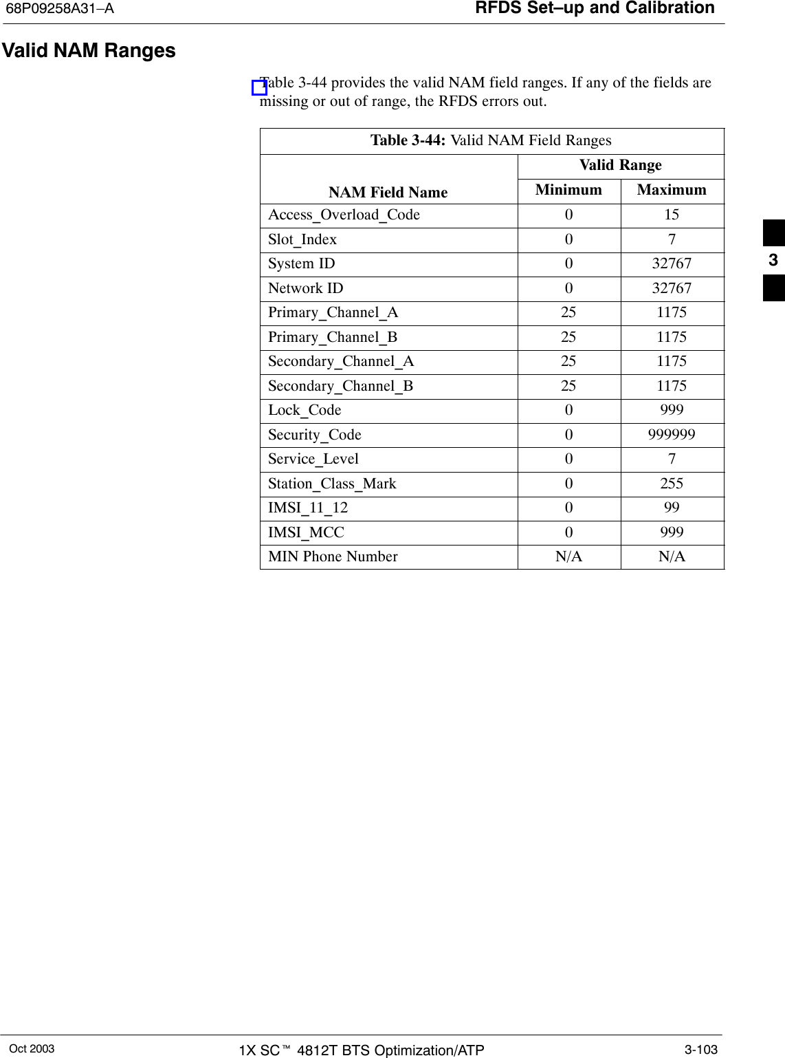
RFDS Set–up and Calibration68P09258A31–AOct 2003 1X SCt 4812T BTS Optimization/ATP 3-103Valid NAM RangesTable 3-44 provides the valid NAM field ranges. If any of the fields aremissing or out of range, the RFDS errors out.Table 3-44: Valid NAM Field RangesValid RangeNAM Field Name Minimum MaximumAccess_Overload_Code 0 15Slot_Index 0 7System ID 0 32767Network ID 0 32767Primary_Channel_A 25 1175Primary_Channel_B 25 1175Secondary_Channel_A 25 1175Secondary_Channel_B 25 1175Lock_Code 0 999Security_Code 0 999999Service_Level 0 7Station_Class_Mark 0 255IMSI_11_12 0 99IMSI_MCC 0 999MIN Phone Number N/A N/A3
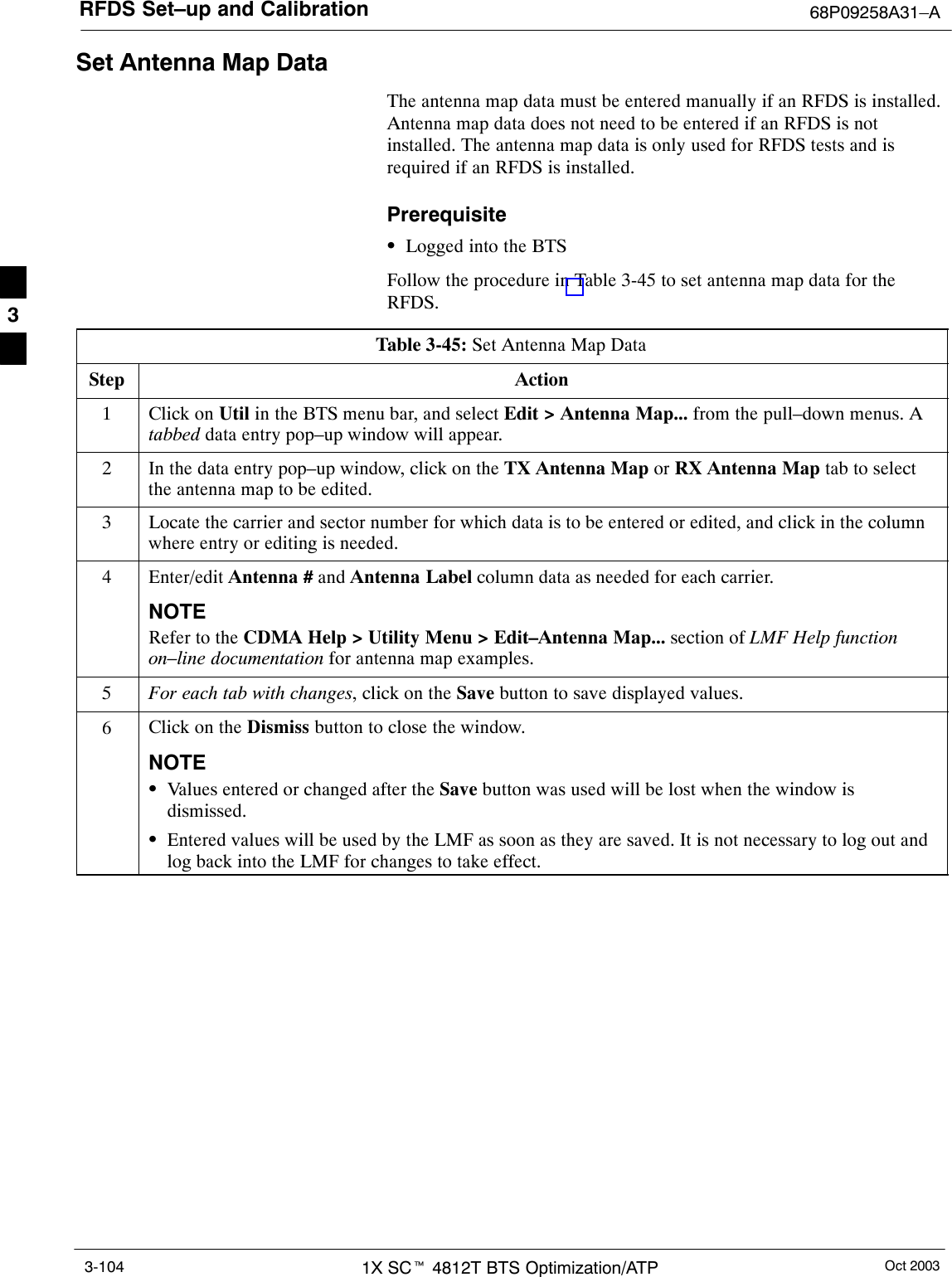
RFDS Set–up and Calibration 68P09258A31–AOct 20031X SCt 4812T BTS Optimization/ATP3-104Set Antenna Map DataThe antenna map data must be entered manually if an RFDS is installed.Antenna map data does not need to be entered if an RFDS is notinstalled. The antenna map data is only used for RFDS tests and isrequired if an RFDS is installed.PrerequisiteSLogged into the BTSFollow the procedure in Table 3-45 to set antenna map data for theRFDS.Table 3-45: Set Antenna Map DataStep Action1Click on Util in the BTS menu bar, and select Edit > Antenna Map... from the pull–down menus. Atabbed data entry pop–up window will appear.2In the data entry pop–up window, click on the TX Antenna Map or RX Antenna Map tab to selectthe antenna map to be edited.3Locate the carrier and sector number for which data is to be entered or edited, and click in the columnwhere entry or editing is needed.4Enter/edit Antenna # and Antenna Label column data as needed for each carrier.NOTERefer to the CDMA Help > Utility Menu > Edit–Antenna Map... section of LMF Help functionon–line documentation for antenna map examples.5For each tab with changes, click on the Save button to save displayed values.6Click on the Dismiss button to close the window.NOTESValues entered or changed after the Save button was used will be lost when the window isdismissed.SEntered values will be used by the LMF as soon as they are saved. It is not necessary to log out andlog back into the LMF for changes to take effect. 3
RFDS Set–up and Calibration68P09258A31–AOct 2003 1X SCt 4812T BTS Optimization/ATP 3-105Set RFDS Configuration DataIf an RFDS is installed, the RFDS configuration data must be manuallyentered.PrerequisiteSLMF is logged into the BTSNOTE The entered antenna# index numbers must correspond to theantenna# index numbers used in the antenna maps.Follow the procedure in Table 3-46 to set the RFDS Configuration Data.Table 3-46: Set RFDS Configuration DataStep Action1Click on Util in the BTS menu bar, and select Edit > RFDS Configuration... from the pull–downmenus. A tabbed data entry pop–up window will appear.2In the data entry pop–up window, click on the TX RFDS Configuration or RX RFDS Configurationtab, as required.3To add a new antenna number, perform the following:3a – Click on the Add Row button.3b – Click in the Antenna #, Cal Antenna, Scap Antenna, or Populate [Y/N] columns, as required.3c – Enter the desired data.4To edit existing values, click in the data box to be changed and change the value.NOTERefer to the CDMA Help > Utility Menu > Edit–RFDS Configuration... section of LMF Helpfunction on–line documentation for RFDS configuration data examples.5To delete a row, click on the row and then click on the Delete Row button.6For each tab with changes, click on the Save button to save displayed values.7Click on the Dismiss button to close the window.NOTESValues entered or changed after the Save button was used will be lost when the window isdismissed.SEntered values will be used by the LMF as soon as they are saved. It is not necessary to log out andlog back into the LMF for changes to take effect.3
RFDS Set–up and Calibration 68P09258A31–AOct 20031X SCt 4812T BTS Optimization/ATP3-106RFDS CalibrationThe RFDS Calibration option is used to calibrate the RFDS TX and RXpaths.TX Path Calibration – For a TX antenna path calibration the BTSXCVR is keyed at a pre–determined power level and the BTS poweroutput level is measured by the RFDS. The power level is then measuredat the TX antenna directional coupler by the power measuring testequipment item being used (power meter or analyzer). The difference(offset) between the power level at the RFDS and the power level at theTX antenna directional coupler is used as the TX RFDS calibrationoffset value.RX Path Calibration – For an RX antenna path calibration the RFDS iskeyed at a pre–determined power level and the power input level ismeasured by the BTS BBX. A CDMA signal at the same power levelmeasured by the BTS BBX is then injected at the RX antenna directionalcoupler by the communications system analyzer. The difference (offset)between the RFDS–keyed power level and power level measured at theBTS BBX is the RFDS RX calibration offset value.RFDS calibration and the CAL file – The TX and RX RFDScalibration offset values are written to the CAL file in the slot[385]Block.TSIC channel frequency – For each RFDS TSIC, the channelfrequency is determined at the lower third and upper third of theappropriate band using the frequencies listed in Table 3-47.Table 3-47: RFDS TSIC Calibration Channel FrequenciesSystem Channel Calibration Points800 MHz (A and B) 341 and 6821.9 GHz 408 and 791WARNING Before installing any test equipment directly to any TX OUTconnector, verify that there are no CDMA channels keyed.Failure to do so can result in serious personal injury and/orequipment damage.PrerequisitesSTest equipment has been selected.STest equipment and test cables have been calibrated.STX calibration has been performed and BLO data has beendownloaded to the BBXs.STest equipment and test cables are connected for TX calibration.SAntenna map data has been entered for the site.SBBXs are OOS–RAM.3
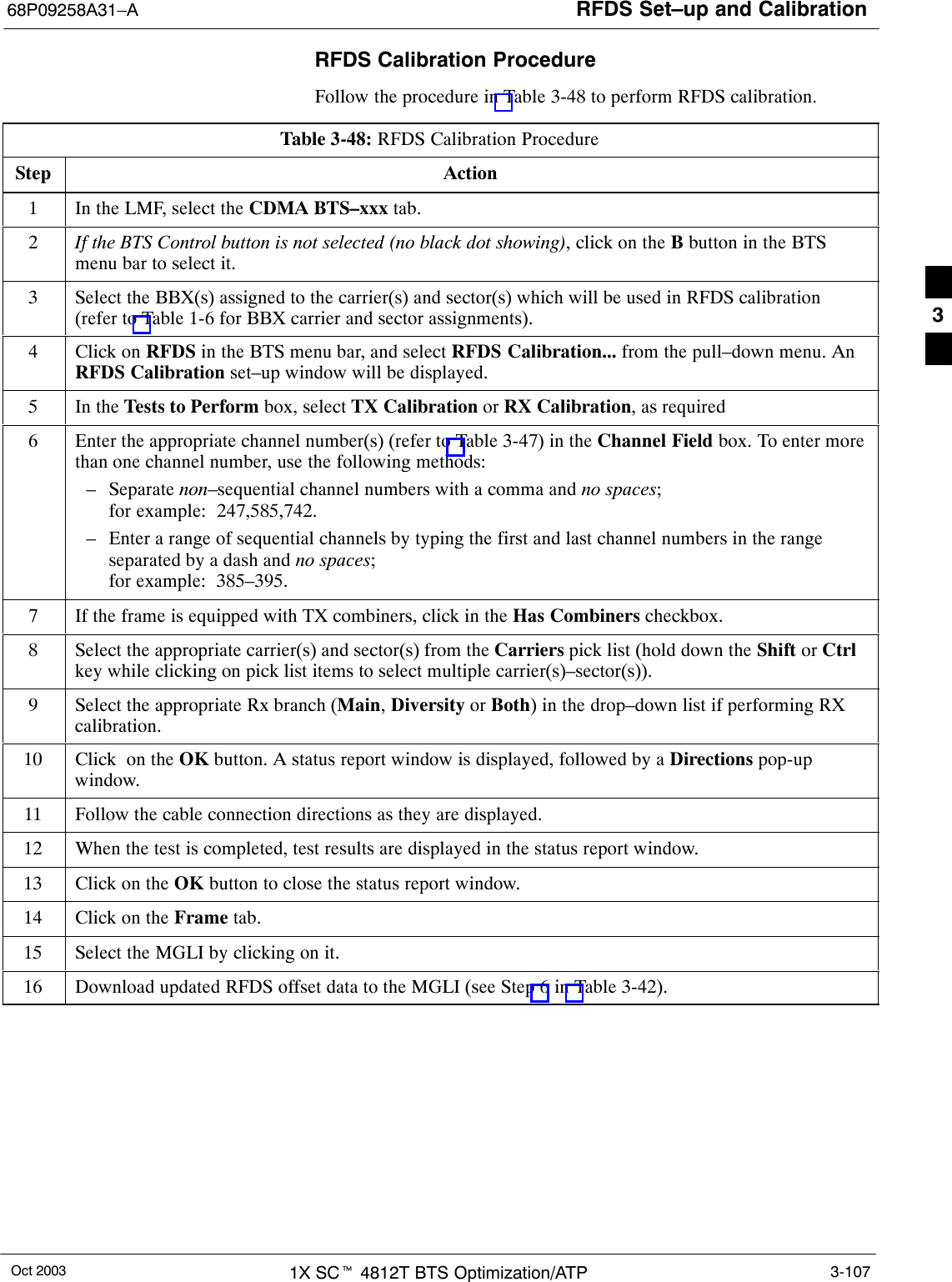
RFDS Set–up and Calibration68P09258A31–AOct 2003 1X SCt 4812T BTS Optimization/ATP 3-107RFDS Calibration ProcedureFollow the procedure in Table 3-48 to perform RFDS calibration.Table 3-48: RFDS Calibration ProcedureStep Action1In the LMF, select the CDMA BTS–xxx tab.2If the BTS Control button is not selected (no black dot showing), click on the B button in the BTSmenu bar to select it.3Select the BBX(s) assigned to the carrier(s) and sector(s) which will be used in RFDS calibration(refer to Table 1-6 for BBX carrier and sector assignments).4Click on RFDS in the BTS menu bar, and select RFDS Calibration... from the pull–down menu. AnRFDS Calibration set–up window will be displayed.5In the Tests to Perform box, select TX Calibration or RX Calibration, as required6Enter the appropriate channel number(s) (refer to Table 3-47) in the Channel Field box. To enter morethan one channel number, use the following methods:– Separate non–sequential channel numbers with a comma and no spaces; for example:  247,585,742.– Enter a range of sequential channels by typing the first and last channel numbers in the rangeseparated by a dash and no spaces; for example:  385–395.7If the frame is equipped with TX combiners, click in the Has Combiners checkbox.8Select the appropriate carrier(s) and sector(s) from the Carriers pick list (hold down the Shift or Ctrlkey while clicking on pick list items to select multiple carrier(s)–sector(s)).9Select the appropriate Rx branch (Main, Diversity or Both) in the drop–down list if performing RXcalibration.10 Click  on the OK button. A status report window is displayed, followed by a Directions pop-upwindow.11 Follow the cable connection directions as they are displayed.12 When the test is completed, test results are displayed in the status report window.13 Click on the OK button to close the status report window.14 Click on the Frame tab.15 Select the MGLI by clicking on it.16 Download updated RFDS offset data to the MGLI (see Step 6 in Table 3-42). 3
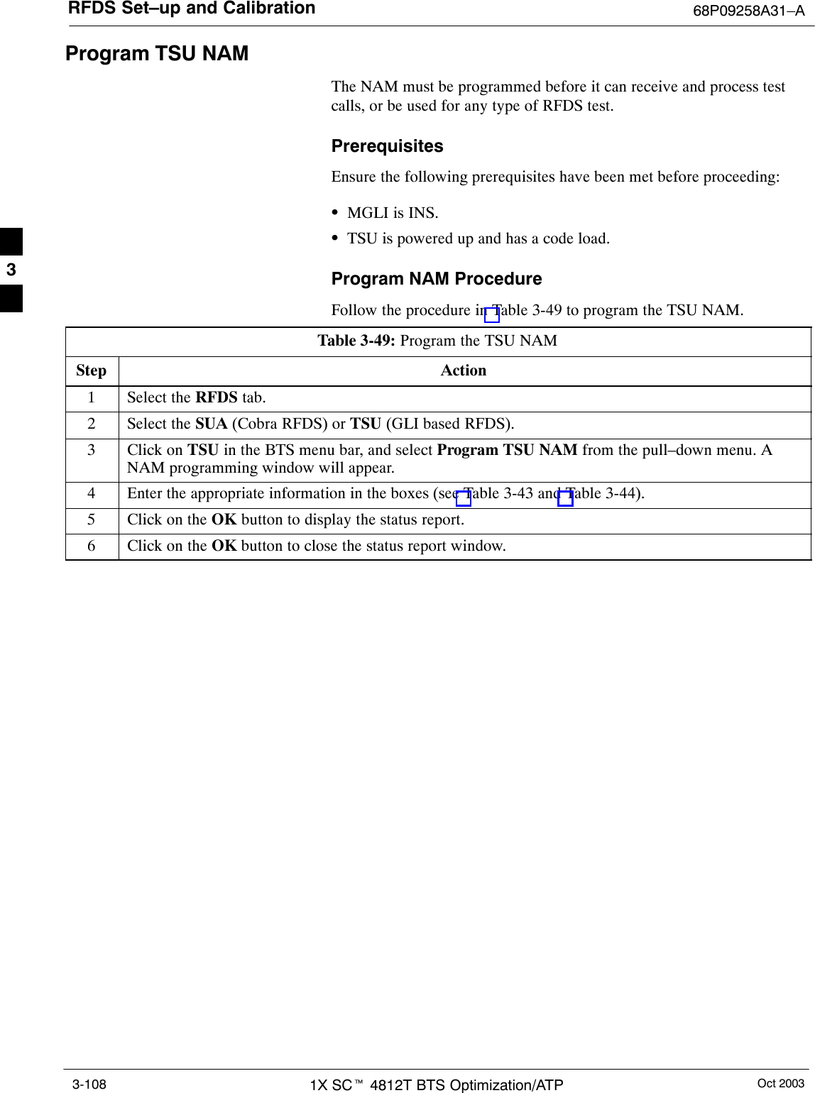
RFDS Set–up and Calibration 68P09258A31–AOct 20031X SCt 4812T BTS Optimization/ATP3-108Program TSU NAMThe NAM must be programmed before it can receive and process testcalls, or be used for any type of RFDS test.PrerequisitesEnsure the following prerequisites have been met before proceeding:SMGLI is INS.STSU is powered up and has a code load.Program NAM ProcedureFollow the procedure in Table 3-49 to program the TSU NAM.Table 3-49: Program the TSU NAMStep Action1Select the RFDS tab.2Select the SUA (Cobra RFDS) or TSU (GLI based RFDS).3Click on TSU in the BTS menu bar, and select Program TSU NAM from the pull–down menu. ANAM programming window will appear.4Enter the appropriate information in the boxes (see Table 3-43 and Table 3-44).5Click on the OK button to display the status report.6Click on the OK button to close the status report window.3
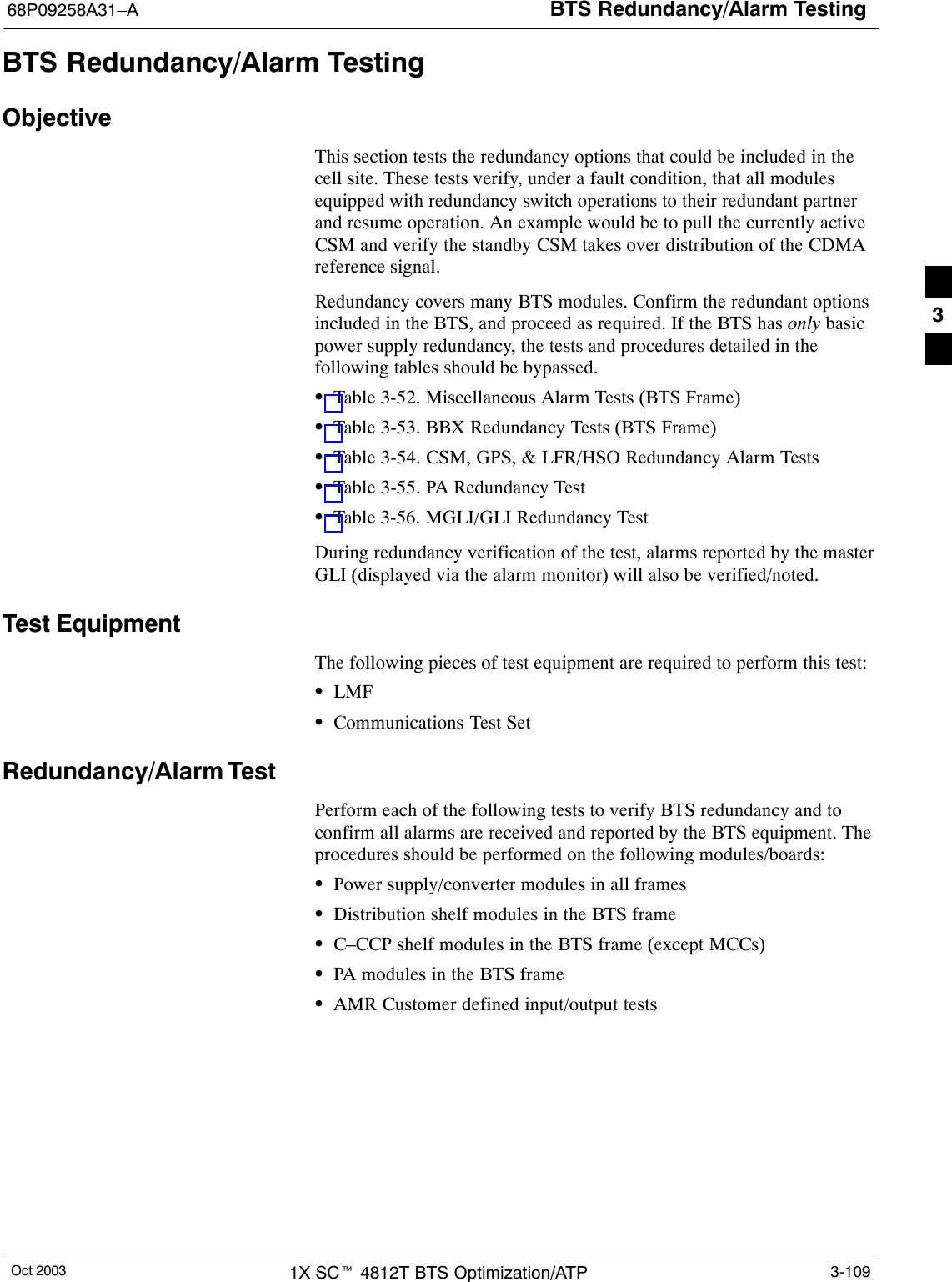
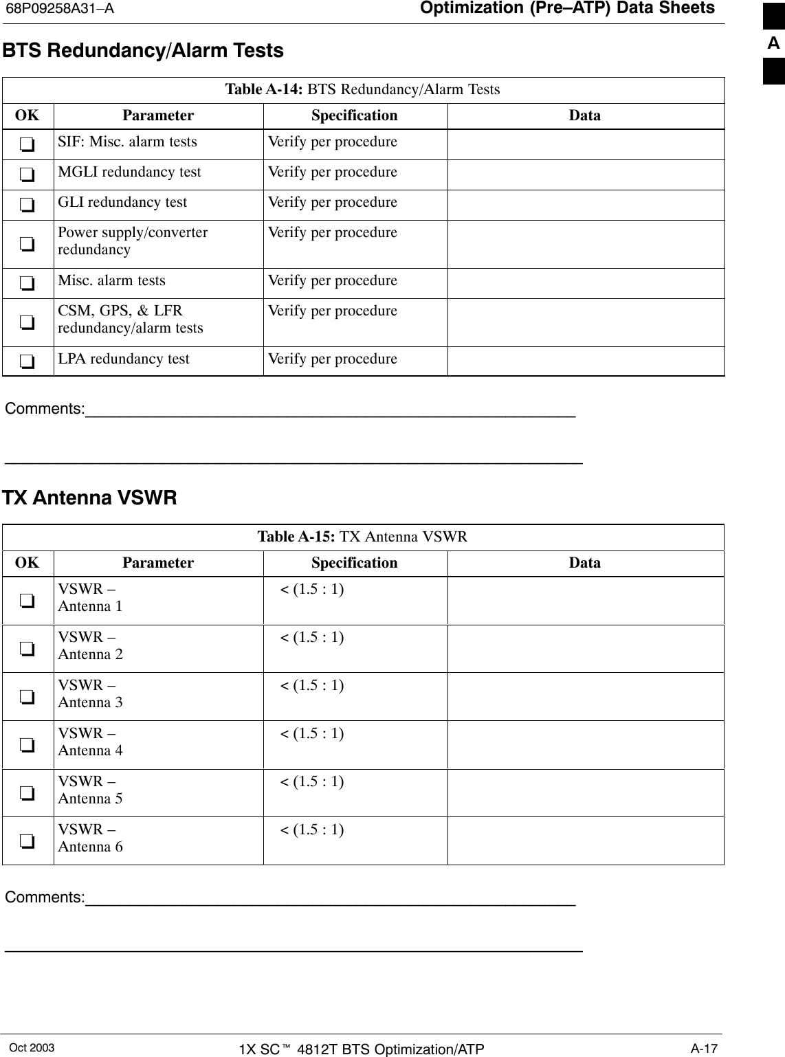
BTS Redundancy/Alarm Testing68P09258A31–AOct 2003 1X SCt 4812T BTS Optimization/ATP 3-109BTS Redundancy/Alarm TestingObjectiveThis section tests the redundancy options that could be included in thecell site. These tests verify, under a fault condition, that all modulesequipped with redundancy switch operations to their redundant partnerand resume operation. An example would be to pull the currently activeCSM and verify the standby CSM takes over distribution of the CDMAreference signal.Redundancy covers many BTS modules. Confirm the redundant optionsincluded in the BTS, and proceed as required. If the BTS has only basicpower supply redundancy, the tests and procedures detailed in thefollowing tables should be bypassed.STable 3-52. Miscellaneous Alarm Tests (BTS Frame)STable 3-53. BBX Redundancy Tests (BTS Frame)STable 3-54. CSM, GPS, & LFR/HSO Redundancy Alarm TestsSTable 3-55. PA Redundancy TestSTable 3-56. MGLI/GLI Redundancy TestDuring redundancy verification of the test, alarms reported by the masterGLI (displayed via the alarm monitor) will also be verified/noted.Test EquipmentThe following pieces of test equipment are required to perform this test:SLMFSCommunications Test SetRedundancy/Alarm TestPerform each of the following tests to verify BTS redundancy and toconfirm all alarms are received and reported by the BTS equipment. Theprocedures should be performed on the following modules/boards:SPower supply/converter modules in all framesSDistribution shelf modules in the BTS frameSC–CCP shelf modules in the BTS frame (except MCCs)SPA modules in the BTS frameSAMR Customer defined input/output tests3
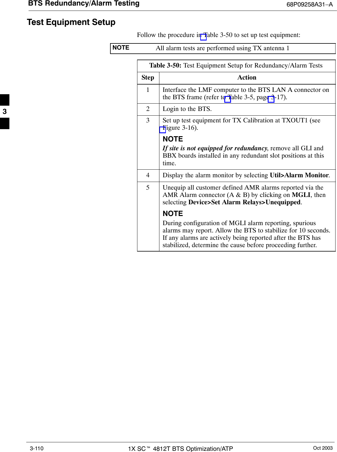
BTS Redundancy/Alarm Testing 68P09258A31–AOct 20031X SCt 4812T BTS Optimization/ATP3-110Test Equipment SetupFollow the procedure in Table 3-50 to set up test equipment:NOTE All alarm tests are performed using TX antenna 1Table 3-50: Test Equipment Setup for Redundancy/Alarm TestsStep Action1Interface the LMF computer to the BTS LAN A connector onthe BTS frame (refer to Table 3-5, page 3-17).2Login to the BTS.3Set up test equipment for TX Calibration at TXOUT1 (seeFigure 3-16).NOTEIf site is not equipped for redundancy, remove all GLI andBBX boards installed in any redundant slot positions at thistime.4Display the alarm monitor by selecting Util>Alarm Monitor.5Unequip all customer defined AMR alarms reported via theAMR Alarm connector (A & B) by clicking on MGLI, thenselecting Device>Set Alarm Relays>Unequipped.NOTEDuring configuration of MGLI alarm reporting, spuriousalarms may report. Allow the BTS to stabilize for 10 seconds.If any alarms are actively being reported after the BTS hasstabilized, determine the cause before proceeding further.3
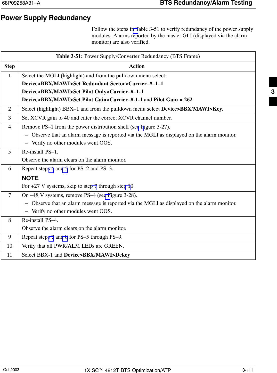
BTS Redundancy/Alarm Testing68P09258A31–AOct 2003 1X SCt 4812T BTS Optimization/ATP 3-111Power Supply RedundancyFollow the steps in Table 3-51 to verify redundancy of the power supplymodules. Alarms reported by the master GLI (displayed via the alarmmonitor) are also verified.Table 3-51: Power Supply/Converter Redundancy (BTS Frame)Step Action1Select the MGLI (highlight) and from the pulldown menu select:Device>BBX/MAWI>Set Redundant Sector>Carrier–#–1–1Device>BBX/MAWI>Set Pilot Only>Carrier–#–1-1Device>BBX/MAWI>Set Pilot Gain>Carrier–#-1-1 and Pilot Gain = 2622Select (highlight) BBX–1 and from the pulldown menu select Device>BBX/MAWI>Key.3Set XCVR gain to 40 and enter the correct XCVR channel number.4Remove PS–1 from the power distribution shelf (see Figure 3-27).– Observe that an alarm message is reported via the MGLI as displayed on the alarm monitor.– Verify no other modules went OOS.5Re-install PS–1.Observe the alarm clears on the alarm monitor.6Repeat steps 4 and 5 for PS–2 and PS–3.NOTEFor +27 V systems, skip to step 7 through step 10.7On –48 V systems, remove PS–4 (see Figure 3-28).– Observe that an alarm message is reported via the MGLI as displayed on the alarm monitor.– Verify no other modules went OOS.8Re-install PS–4.Observe the alarm clears on the alarm monitor.9Repeat steps 7 and 8 for PS–5 through PS–9.10 Verify that all PWR/ALM LEDs are GREEN.11 Select BBX-1 and Device>BBX/MAWI>Dekey 3
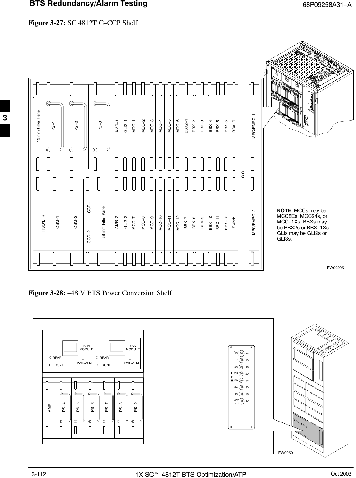
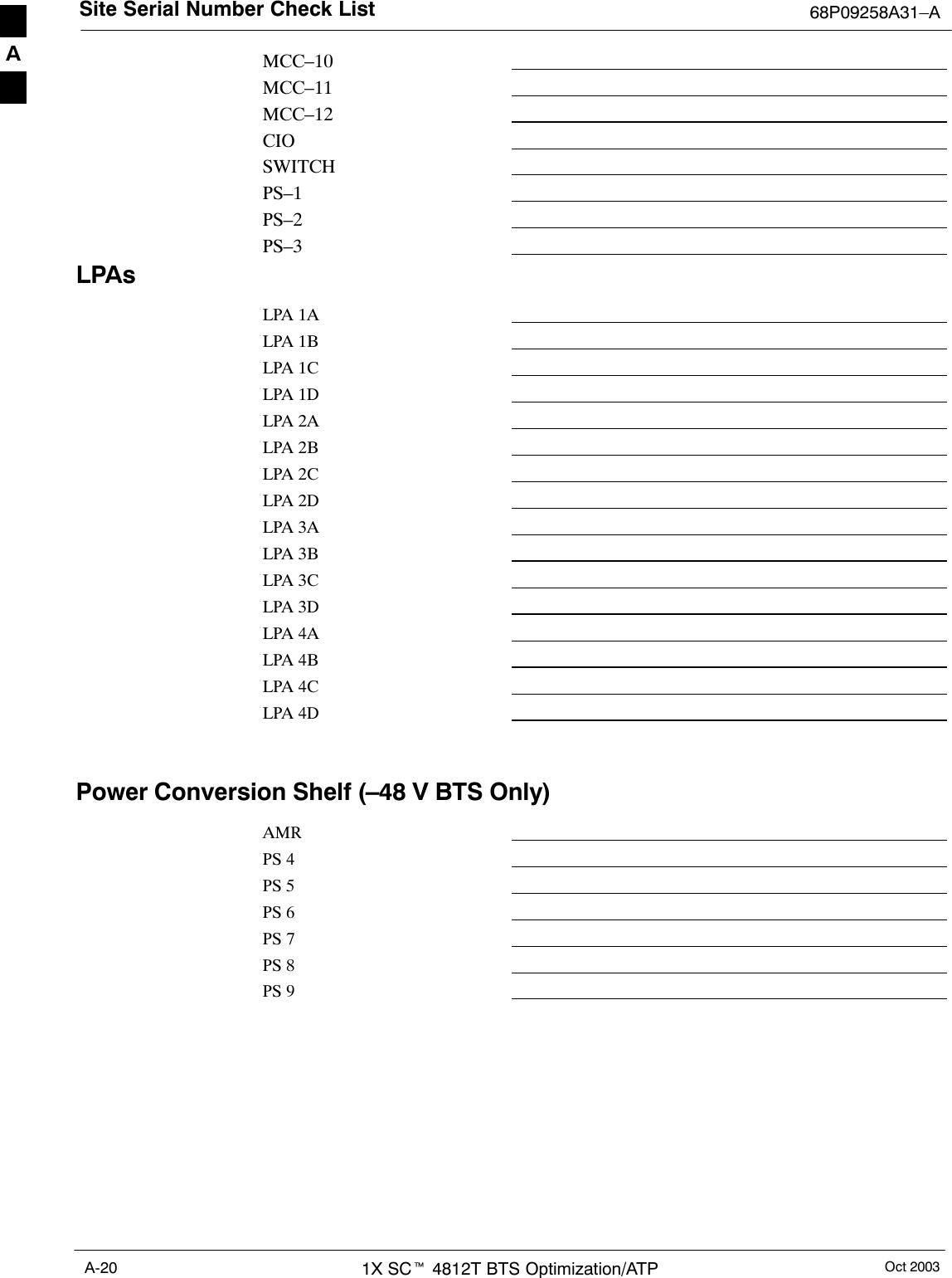
BTS Redundancy/Alarm Testing 68P09258A31–AOct 20031X SCt 4812T BTS Optimization/ATP3-112Figure 3-27: SC 4812T C–CCP Shelf19 mm Filler PanelPS–3AMR–1CSM–1CSM–238 mm Filler PanelAMR–2GLI2–1GLI2–2MCC–6BBX2–1BBX–2BBX–3BBX–4BBX–5BBX–6BBX–RSwitchMPC/EMPC–1MPC/EMPC–2CIOBBX–7BBX–8BBX–9BBX–10BBX–11BBX–12MCC–5MCC–4MCC–3MCC–2MCC–1MCC–12MCC–11MCC–10MCC–9MCC–8MCC–7PS–2PS–1CCD–2 CCD–1NOTE: MCCs may beMCC8Es, MCC24s, orMCC–1Xs. BBXs maybe BBX2s or BBX–1Xs.GLIs may be GLI2s orGLI3s.HSO/LFRFW00295Figure 3-28: –48 V BTS Power Conversion ShelfFW00501PS–6AMRPS–5PS–4PS–9PS–8PS–71C1A2A2C3C3A4A4CLPA1D1B2B2D3D3B4B4D3030303030303030FANMODULEPWR/ALMREARFRONTFANMODULEPWR/ALMREARFRONT3
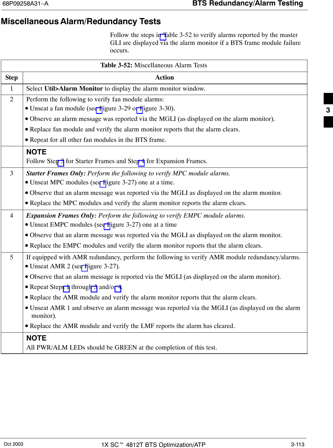
BTS Redundancy/Alarm Testing68P09258A31–AOct 2003 1X SCt 4812T BTS Optimization/ATP 3-113Miscellaneous Alarm/Redundancy TestsFollow the steps in Table 3-52 to verify alarms reported by the masterGLI are displayed via the alarm monitor if a BTS frame module failureoccurs.Table 3-52: Miscellaneous Alarm TestsStep Action1 Select Util>Alarm Monitor to display the alarm monitor window.2Perform the following to verify fan module alarms:•Unseat a fan module (see Figure 3-29 or Figure 3-30).•Observe an alarm message was reported via the MGLI (as displayed on the alarm monitor).•Replace fan module and verify the alarm monitor reports that the alarm clears.•Repeat for all other fan modules in the BTS frame.NOTEFollow Step 3 for Starter Frames and Step 4 for Expansion Frames.3Starter Frames Only: Perform the following to verify MPC module alarms.•Unseat MPC modules (see Figure 3-27) one at a time.•Observe that an alarm message was reported via the MGLI as displayed on the alarm monitor.•Replace the MPC modules and verify the alarm monitor reports the alarm clears.4Expansion Frames Only: Perform the following to verify EMPC module alarms.•Unseat EMPC modules (see Figure 3-27) one at a time•Observe that an alarm message was reported via the MGLI as displayed on the alarm monitor.•Replace the EMPC modules and verify the alarm monitor reports that the alarm clears.5If equipped with AMR redundancy, perform the following to verify AMR module redundancy/alarms.•Unseat AMR 2 (see Figure 3-27).•Observe that an alarm message is reported via the MGLI (as displayed on the alarm monitor).•Repeat Steps 1 through 3 and/or 4.•Replace the AMR module and verify the alarm monitor reports that the alarm clears.•Unseat AMR 1 and observe an alarm message was reported via the MGLI (as displayed on the alarmmonitor).•Replace the AMR module and verify the LMF reports the alarm has cleared.NOTEAll PWR/ALM LEDs should be GREEN at the completion of this test. 3
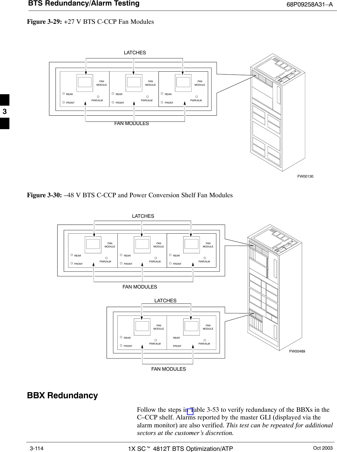
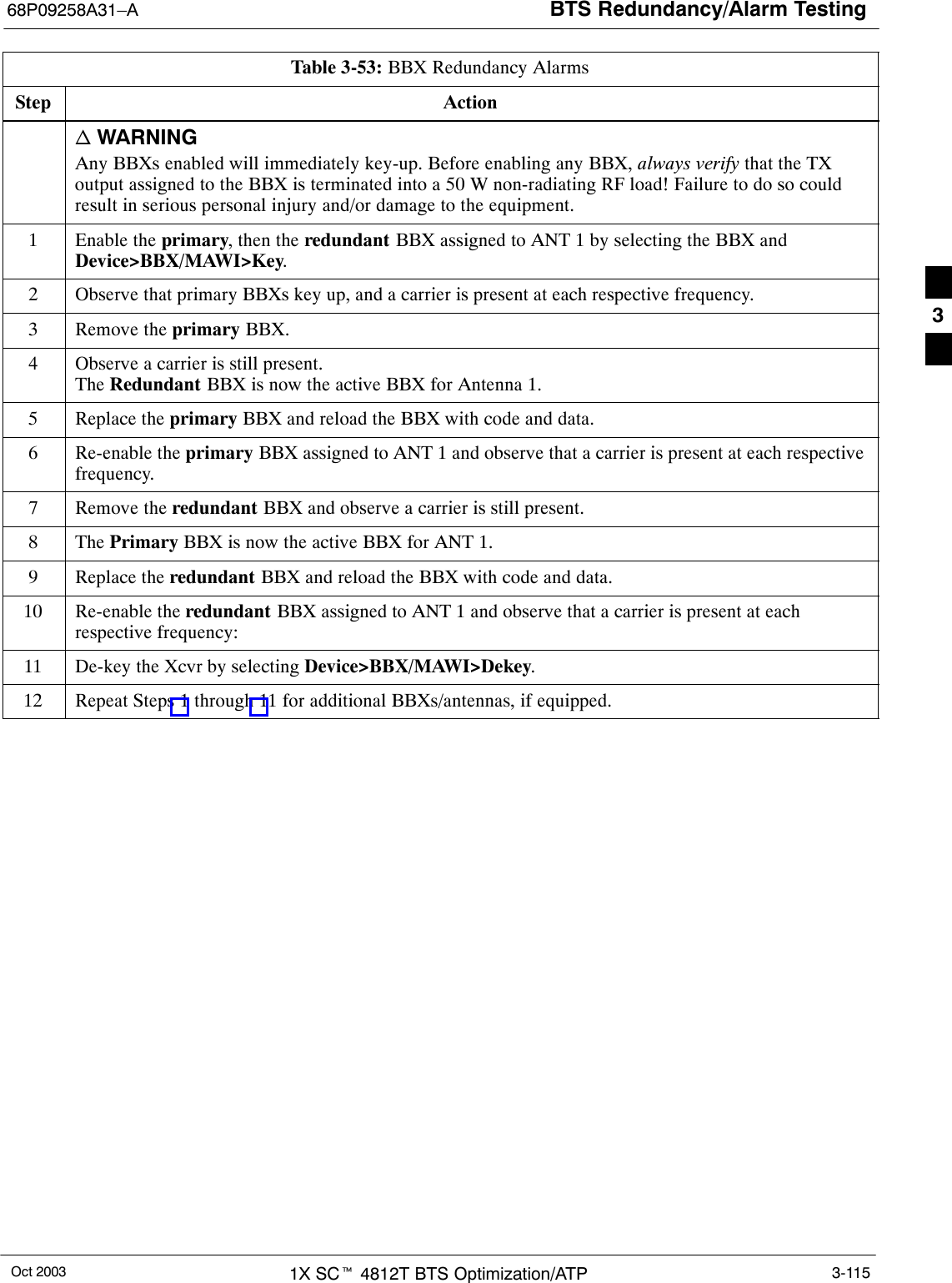
BTS Redundancy/Alarm Testing 68P09258A31–AOct 20031X SCt 4812T BTS Optimization/ATP3-114Figure 3-29: +27 V BTS C-CCP Fan ModulesFANMODULEPWR/ALMREARFRONTFANMODULEPWR/ALMREARFRONTFANMODULEPWR/ALMREARFRONTFAN MODULESLATCHESFW00130Figure 3-30: –48 V BTS C-CCP and Power Conversion Shelf Fan ModulesFANMODULEPWR/ALMREARFRONTFANMODULEPWR/ALMREARFRONTFANMODULEPWR/ALMREARFRONTFAN MODULESLATCHESFW00489FAN MODULESLATCHESFANMODULEPWR/ALMREARFRONTFANMODULEPWR/ALMREARFRONTBBX RedundancyFollow the steps in Table 3-53 to verify redundancy of the BBXs in theC–CCP shelf. Alarms reported by the master GLI (displayed via thealarm monitor) are also verified. This test can be repeated for additionalsectors at the customer’s discretion.3
BTS Redundancy/Alarm Testing68P09258A31–AOct 2003 1X SCt 4812T BTS Optimization/ATP 3-115Table 3-53: BBX Redundancy AlarmsStep Actionn WARNINGAny BBXs enabled will immediately key-up. Before enabling any BBX, always verify that the TXoutput assigned to the BBX is terminated into a 50 W non-radiating RF load! Failure to do so couldresult in serious personal injury and/or damage to the equipment.1Enable the primary, then the redundant BBX assigned to ANT 1 by selecting the BBX andDevice>BBX/MAWI>Key.2Observe that primary BBXs key up, and a carrier is present at each respective frequency.3Remove the primary BBX.4Observe a carrier is still present.The Redundant BBX is now the active BBX for Antenna 1.5Replace the primary BBX and reload the BBX with code and data.6Re-enable the primary BBX assigned to ANT 1 and observe that a carrier is present at each respectivefrequency.7Remove the redundant BBX and observe a carrier is still present.8 The Primary BBX is now the active BBX for ANT 1.9Replace the redundant BBX and reload the BBX with code and data.10 Re-enable the redundant BBX assigned to ANT 1 and observe that a carrier is present at eachrespective frequency:11 De-key the Xcvr by selecting Device>BBX/MAWI>Dekey.12 Repeat Steps 1 through 11 for additional BBXs/antennas, if equipped. 3
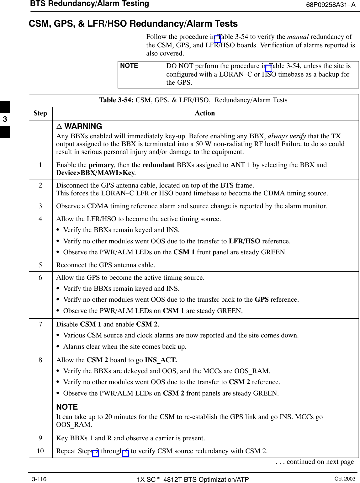
BTS Redundancy/Alarm Testing 68P09258A31–AOct 20031X SCt 4812T BTS Optimization/ATP3-116CSM, GPS, & LFR/HSO Redundancy/Alarm TestsFollow the procedure in Table 3-54 to verify the manual redundancy ofthe CSM, GPS, and LFR/HSO boards. Verification of alarms reported isalso covered.NOTE DO NOT perform the procedure in Table 3-54, unless the site isconfigured with a LORAN–C or HSO timebase as a backup forthe GPS.Table 3-54: CSM, GPS, & LFR/HSO,  Redundancy/Alarm TestsStep Actionn WARNINGAny BBXs enabled will immediately key-up. Before enabling any BBX, always verify that the TXoutput assigned to the BBX is terminated into a 50 W non-radiating RF load! Failure to do so couldresult in serious personal injury and/or damage to the equipment.1Enable the primary, then the redundant BBXs assigned to ANT 1 by selecting the BBX andDevice>BBX/MAWI>Key.2Disconnect the GPS antenna cable, located on top of the BTS frame.This forces the LORAN–C LFR or HSO board timebase to become the CDMA timing source.3Observe a CDMA timing reference alarm and source change is reported by the alarm monitor.4Allow the LFR/HSO to become the active timing source.SVerify the BBXs remain keyed and INS.SVerify no other modules went OOS due to the transfer to LFR/HSO reference.SObserve the PWR/ALM LEDs on the CSM 1 front panel are steady GREEN.5Reconnect the GPS antenna cable.6Allow the GPS to become the active timing source.SVerify the BBXs remain keyed and INS.SVerify no other modules went OOS due to the transfer back to the GPS reference.SObserve the PWR/ALM LEDs on CSM 1 are steady GREEN.7 Disable CSM 1 and enable CSM 2.SVarious CSM source and clock alarms are now reported and the site comes down.SAlarms clear when the site comes back up.8Allow the CSM 2 board to go INS_ACT.SVerify the BBXs are dekeyed and OOS, and the MCCs are OOS_RAM.SVerify no other modules went OOS due to the transfer to CSM 2 reference.SObserve the PWR/ALM LEDs on CSM 2 front panels are steady GREEN.NOTEIt can take up to 20 minutes for the CSM to re-establish the GPS link and go INS. MCCs goOOS_RAM.9Key BBXs 1 and R and observe a carrier is present.10 Repeat Steps 2 through 6 to verify CSM source redundancy with CSM 2.. . . continued on next page3
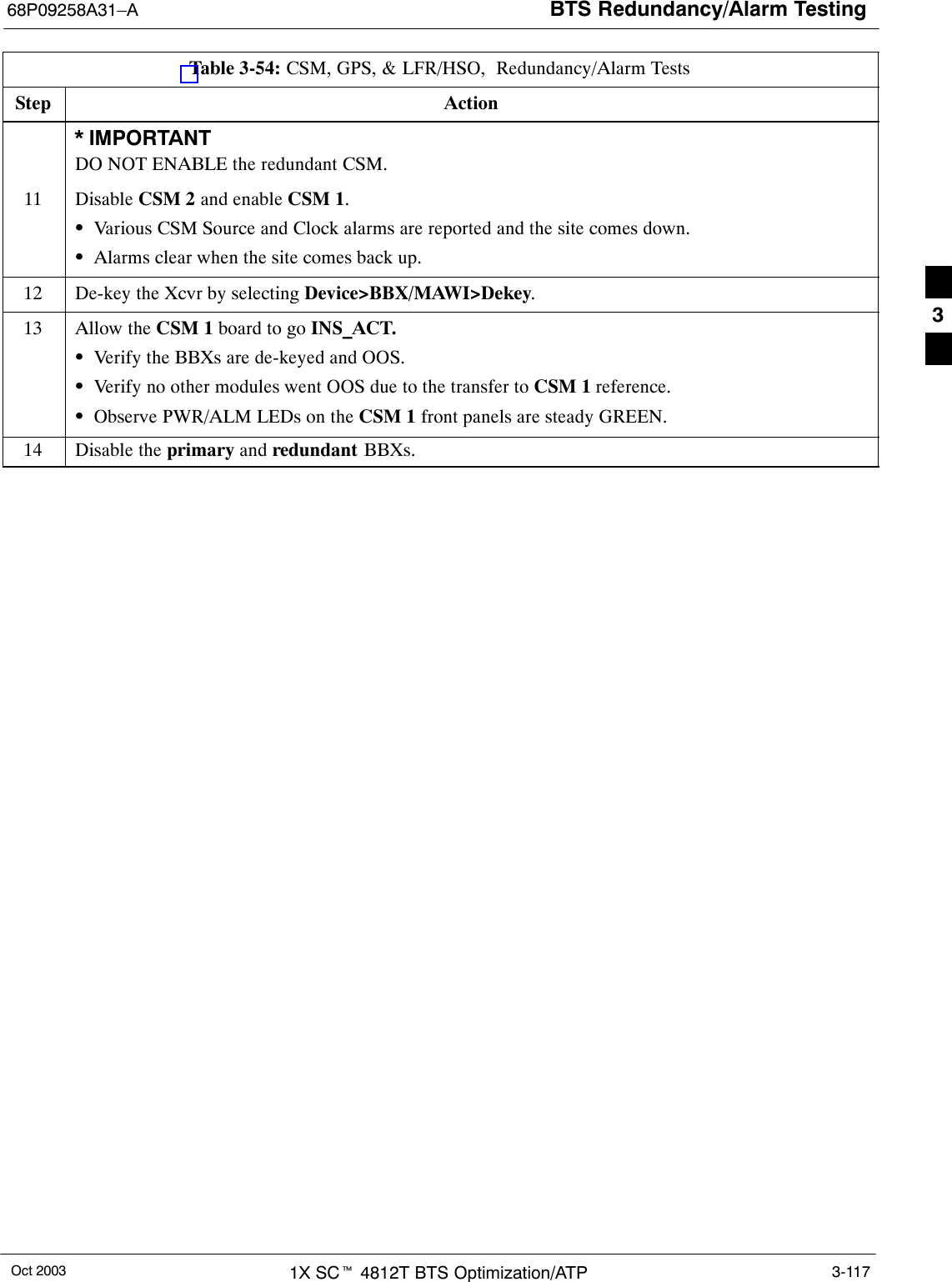
BTS Redundancy/Alarm Testing68P09258A31–AOct 2003 1X SCt 4812T BTS Optimization/ATP 3-117Table 3-54: CSM, GPS, & LFR/HSO,  Redundancy/Alarm TestsStep Action* IMPORTANTDO NOT ENABLE the redundant CSM.11 Disable CSM 2 and enable CSM 1.SVarious CSM Source and Clock alarms are reported and the site comes down.SAlarms clear when the site comes back up.12 De-key the Xcvr by selecting Device>BBX/MAWI>Dekey.13 Allow the CSM 1 board to go INS_ACT.SVerify the BBXs are de-keyed and OOS.SVerify no other modules went OOS due to the transfer to CSM 1 reference.SObserve PWR/ALM LEDs on the CSM 1 front panels are steady GREEN.14 Disable the primary and redundant BBXs. 3
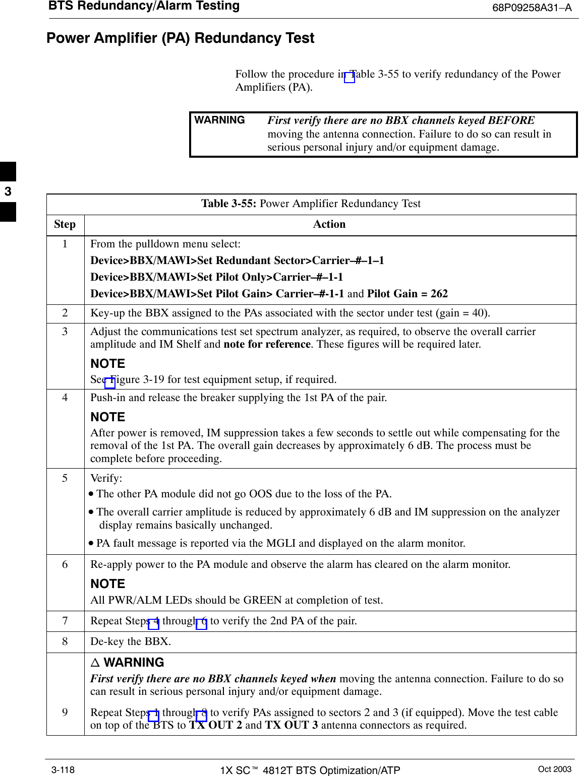
BTS Redundancy/Alarm Testing 68P09258A31–AOct 20031X SCt 4812T BTS Optimization/ATP3-118Power Amplifier (PA) Redundancy TestFollow the procedure in Table 3-55 to verify redundancy of the PowerAmplifiers (PA).WARNING First verify there are no BBX channels keyed BEFOREmoving the antenna connection. Failure to do so can result inserious personal injury and/or equipment damage.Table 3-55: Power Amplifier Redundancy TestStep Action1From the pulldown menu select:Device>BBX/MAWI>Set Redundant Sector>Carrier–#–1–1Device>BBX/MAWI>Set Pilot Only>Carrier–#–1-1Device>BBX/MAWI>Set Pilot Gain> Carrier–#-1-1 and Pilot Gain = 2622Key-up the BBX assigned to the PAs associated with the sector under test (gain = 40).3Adjust the communications test set spectrum analyzer, as required, to observe the overall carrieramplitude and IM Shelf and note for reference. These figures will be required later.NOTESee Figure 3-19 for test equipment setup, if required.4Push-in and release the breaker supplying the 1st PA of the pair.NOTEAfter power is removed, IM suppression takes a few seconds to settle out while compensating for theremoval of the 1st PA. The overall gain decreases by approximately 6 dB. The process must becomplete before proceeding.5 Verify:•The other PA module did not go OOS due to the loss of the PA.•The overall carrier amplitude is reduced by approximately 6 dB and IM suppression on the analyzerdisplay remains basically unchanged.•PA fault message is reported via the MGLI and displayed on the alarm monitor.6Re-apply power to the PA module and observe the alarm has cleared on the alarm monitor.NOTEAll PWR/ALM LEDs should be GREEN at completion of test.7Repeat Steps 4 through 6 to verify the 2nd PA of the pair.8De-key the BBX.n WARNINGFirst verify there are no BBX channels keyed when moving the antenna connection. Failure to do socan result in serious personal injury and/or equipment damage.9Repeat Steps 1 through 8 to verify PAs assigned to sectors 2 and 3 (if equipped). Move the test cableon top of the BTS to TX OUT 2 and TX OUT 3 antenna connectors as required. 3
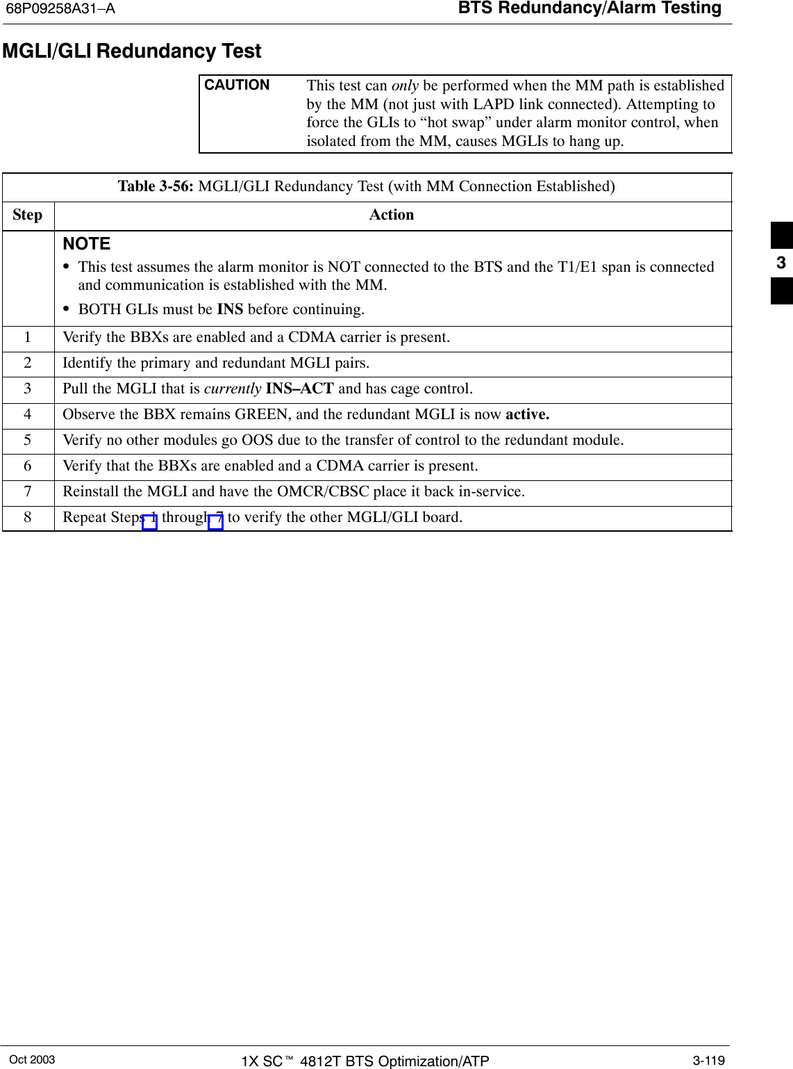
BTS Redundancy/Alarm Testing68P09258A31–AOct 2003 1X SCt 4812T BTS Optimization/ATP 3-119MGLI/GLI Redundancy TestCAUTION This test can only be performed when the MM path is establishedby the MM (not just with LAPD link connected). Attempting toforce the GLIs to “hot swap” under alarm monitor control, whenisolated from the MM, causes MGLIs to hang up.Table 3-56: MGLI/GLI Redundancy Test (with MM Connection Established)Step ActionNOTESThis test assumes the alarm monitor is NOT connected to the BTS and the T1/E1 span is connectedand communication is established with the MM.SBOTH GLIs must be INS before continuing.1Verify the BBXs are enabled and a CDMA carrier is present.2Identify the primary and redundant MGLI pairs.3Pull the MGLI that is currently INS–ACT and has cage control.4Observe the BBX remains GREEN, and the redundant MGLI is now active.5Verify no other modules go OOS due to the transfer of control to the redundant module.6Verify that the BBXs are enabled and a CDMA carrier is present.7Reinstall the MGLI and have the OMCR/CBSC place it back in-service.8Repeat Steps 1 through 7 to verify the other MGLI/GLI board.3
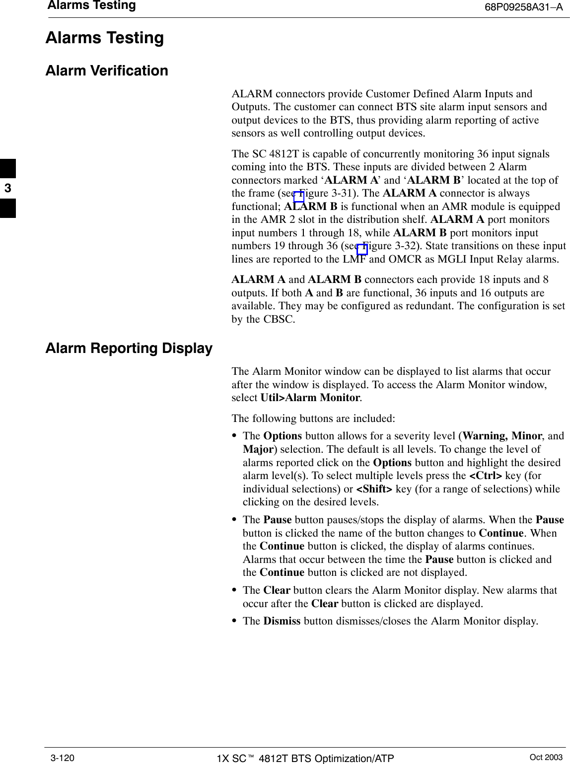
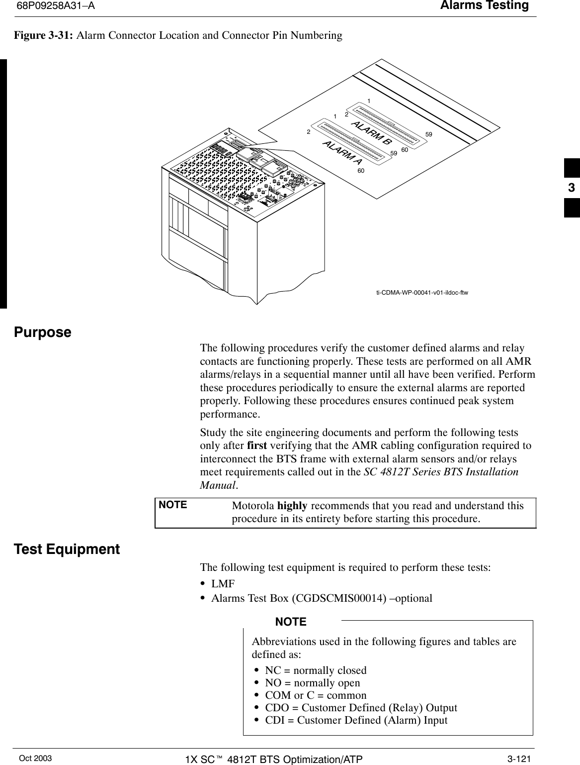
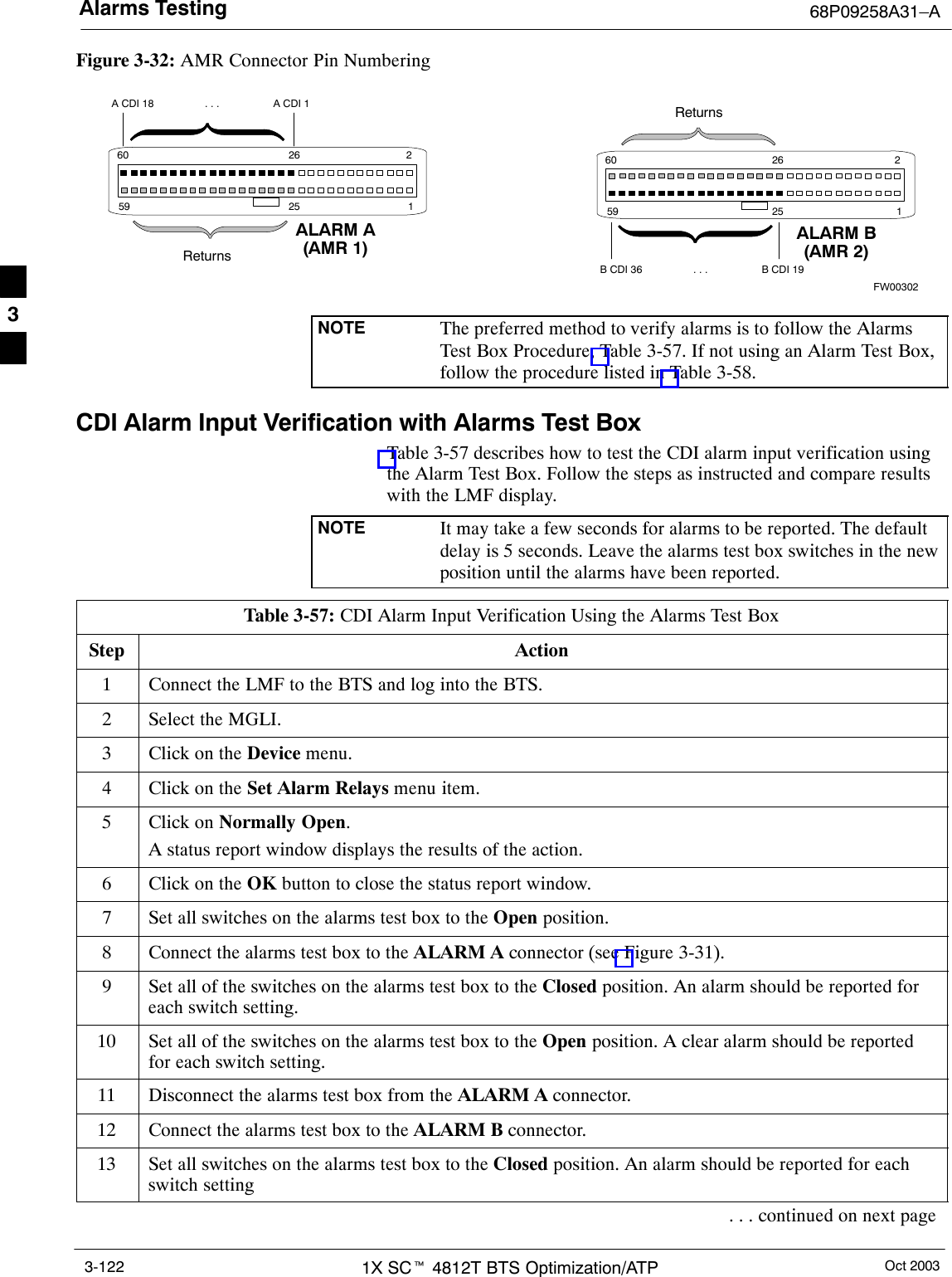
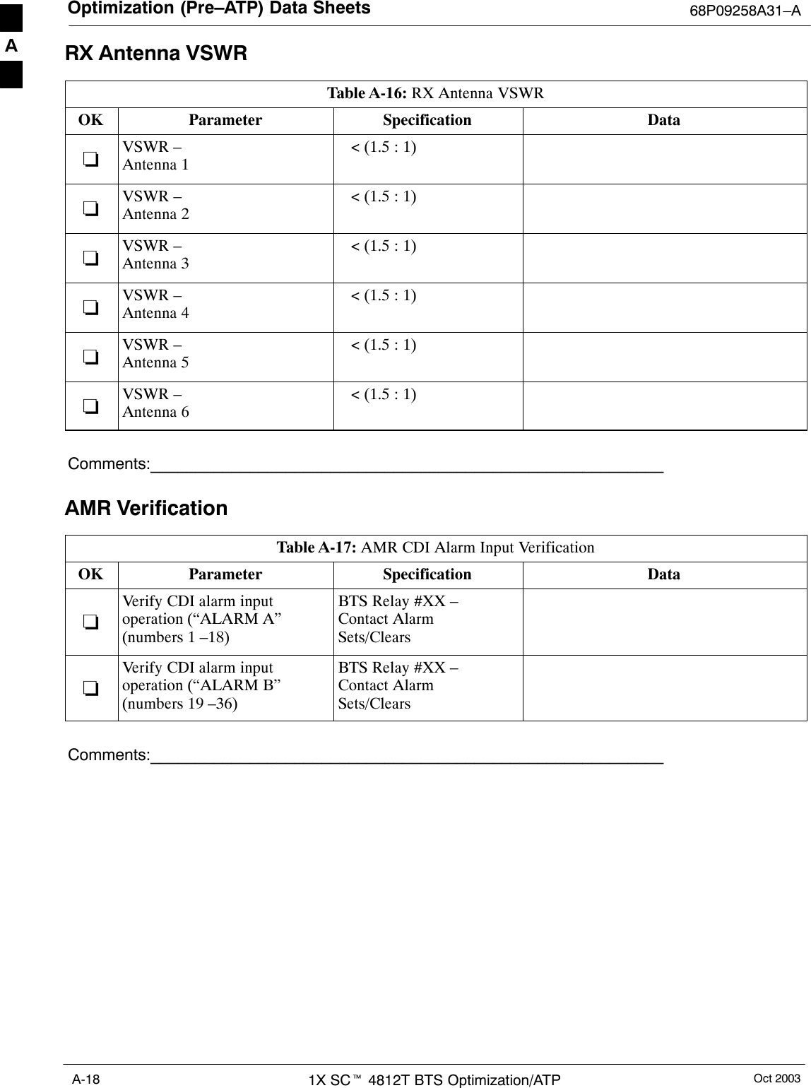
Alarms Testing 68P09258A31–AOct 20031X SCt 4812T BTS Optimization/ATP3-120Alarms TestingAlarm VerificationALARM connectors provide Customer Defined Alarm Inputs andOutputs. The customer can connect BTS site alarm input sensors andoutput devices to the BTS, thus providing alarm reporting of activesensors as well controlling output devices.The SC 4812T is capable of concurrently monitoring 36 input signalscoming into the BTS. These inputs are divided between 2 Alarmconnectors marked ‘ALARM A’ and ‘ALARM B’ located at the top ofthe frame (see Figure 3-31). The ALARM A connector is alwaysfunctional; ALARM B is functional when an AMR module is equippedin the AMR 2 slot in the distribution shelf. ALARM A port monitorsinput numbers 1 through 18, while ALARM B port monitors inputnumbers 19 through 36 (see Figure 3-32). State transitions on these inputlines are reported to the LMF and OMCR as MGLI Input Relay alarms.ALARM A and ALARM B connectors each provide 18 inputs and 8outputs. If both A and B are functional, 36 inputs and 16 outputs areavailable. They may be configured as redundant. The configuration is setby the CBSC.Alarm Reporting DisplayThe Alarm Monitor window can be displayed to list alarms that occurafter the window is displayed. To access the Alarm Monitor window,select Util>Alarm Monitor.The following buttons are included:SThe Options button allows for a severity level (Warning, Minor, andMajor) selection. The default is all levels. To change the level ofalarms reported click on the Options button and highlight the desiredalarm level(s). To select multiple levels press the <Ctrl> key (forindividual selections) or <Shift> key (for a range of selections) whileclicking on the desired levels.SThe Pause button pauses/stops the display of alarms. When the Pausebutton is clicked the name of the button changes to Continue. Whenthe Continue button is clicked, the display of alarms continues.Alarms that occur between the time the Pause button is clicked andthe Continue button is clicked are not displayed.SThe Clear button clears the Alarm Monitor display. New alarms thatoccur after the Clear button is clicked are displayed.SThe Dismiss button dismisses/closes the Alarm Monitor display.3
Alarms Testing68P09258A31–AOct 2003 1X SCt 4812T BTS Optimization/ATP 3-121Figure 3-31: Alarm Connector Location and Connector Pin Numberingti-CDMA-WP-00041-v01-ildoc-ftw591602591602PurposeThe following procedures verify the customer defined alarms and relaycontacts are functioning properly. These tests are performed on all AMRalarms/relays in a sequential manner until all have been verified. Performthese procedures periodically to ensure the external alarms are reportedproperly. Following these procedures ensures continued peak systemperformance.Study the site engineering documents and perform the following testsonly after first verifying that the AMR cabling configuration required tointerconnect the BTS frame with external alarm sensors and/or relaysmeet requirements called out in the SC 4812T Series BTS InstallationManual.NOTE Motorola highly recommends that you read and understand thisprocedure in its entirety before starting this procedure.Test EquipmentThe following test equipment is required to perform these tests:SLMFSAlarms Test Box (CGDSCMIS00014) –optionalAbbreviations used in the following figures and tables aredefined as:SNC = normally closedSNO = normally openSCOM or C = commonSCDO = Customer Defined (Relay) OutputSCDI = Customer Defined (Alarm) InputNOTE3
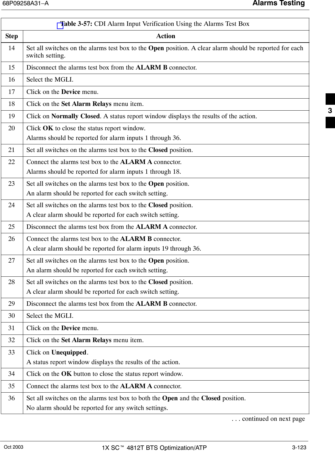
Alarms Testing 68P09258A31–AOct 20031X SCt 4812T BTS Optimization/ATP3-122Figure 3-32: AMR Connector Pin Numbering59 160 2ALARM A(AMR 1) ALARM B(AMR 2)Returns2526A CDI 18 . . . A CDI 159 160 2 Returns2526B CDI 36 . . . B CDI 19FW00302NOTE The preferred method to verify alarms is to follow the AlarmsTest Box Procedure, Table 3-57. If not using an Alarm Test Box,follow the procedure listed in Table 3-58.CDI Alarm Input Verification with Alarms Test BoxTable 3-57 describes how to test the CDI alarm input verification usingthe Alarm Test Box. Follow the steps as instructed and compare resultswith the LMF display.NOTE It may take a few seconds for alarms to be reported. The defaultdelay is 5 seconds. Leave the alarms test box switches in the newposition until the alarms have been reported.Table 3-57: CDI Alarm Input Verification Using the Alarms Test BoxStep Action1Connect the LMF to the BTS and log into the BTS.2Select the MGLI.3Click on the Device menu.4Click on the Set Alarm Relays menu item.5Click on Normally Open.A status report window displays the results of the action.6Click on the OK button to close the status report window.7Set all switches on the alarms test box to the Open position.8Connect the alarms test box to the ALARM A connector (see Figure 3-31).9Set all of the switches on the alarms test box to the Closed position. An alarm should be reported foreach switch setting.10 Set all of the switches on the alarms test box to the Open position. A clear alarm should be reportedfor each switch setting.11 Disconnect the alarms test box from the ALARM A connector.12 Connect the alarms test box to the ALARM B connector.13 Set all switches on the alarms test box to the Closed position. An alarm should be reported for eachswitch setting. . . continued on next page3
Alarms Testing68P09258A31–AOct 2003 1X SCt 4812T BTS Optimization/ATP 3-123Table 3-57: CDI Alarm Input Verification Using the Alarms Test BoxStep Action14 Set all switches on the alarms test box to the Open position. A clear alarm should be reported for eachswitch setting.15 Disconnect the alarms test box from the ALARM B connector.16 Select the MGLI.17 Click on the Device menu.18 Click on the Set Alarm Relays menu item.19 Click on Normally Closed. A status report window displays the results of the action.20 Click OK to close the status report window.Alarms should be reported for alarm inputs 1 through 36.21 Set all switches on the alarms test box to the Closed position.22 Connect the alarms test box to the ALARM A connector.Alarms should be reported for alarm inputs 1 through 18.23 Set all switches on the alarms test box to the Open position.An alarm should be reported for each switch setting.24 Set all switches on the alarms test box to the Closed position.A clear alarm should be reported for each switch setting.25 Disconnect the alarms test box from the ALARM A connector.26 Connect the alarms test box to the ALARM B connector.A clear alarm should be reported for alarm inputs 19 through 36.27 Set all switches on the alarms test box to the Open position.An alarm should be reported for each switch setting.28 Set all switches on the alarms test box to the Closed position.A clear alarm should be reported for each switch setting.29 Disconnect the alarms test box from the ALARM B connector.30 Select the MGLI.31 Click on the Device menu.32 Click on the Set Alarm Relays menu item.33 Click on Unequipped.A status report window displays the results of the action.34 Click on the OK button to close the status report window.35 Connect the alarms test box to the ALARM A connector.36 Set all switches on the alarms test box to both the Open and the Closed position.No alarm should be reported for any switch settings.. . . continued on next page3
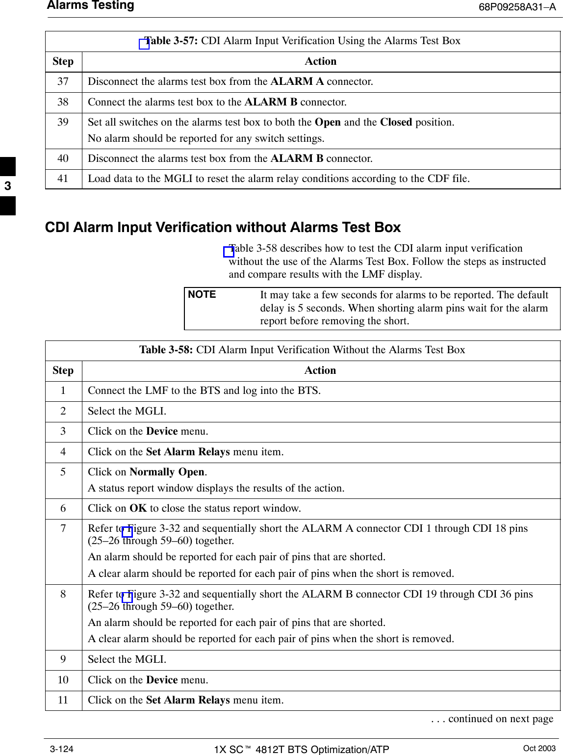
Alarms Testing 68P09258A31–AOct 20031X SCt 4812T BTS Optimization/ATP3-124Table 3-57: CDI Alarm Input Verification Using the Alarms Test BoxStep Action37 Disconnect the alarms test box from the ALARM A connector.38 Connect the alarms test box to the ALARM B connector.39 Set all switches on the alarms test box to both the Open and the Closed position.No alarm should be reported for any switch settings.40 Disconnect the alarms test box from the ALARM B connector.41 Load data to the MGLI to reset the alarm relay conditions according to the CDF file. CDI Alarm Input Verification without Alarms Test BoxTable 3-58 describes how to test the CDI alarm input verificationwithout the use of the Alarms Test Box. Follow the steps as instructedand compare results with the LMF display.NOTE It may take a few seconds for alarms to be reported. The defaultdelay is 5 seconds. When shorting alarm pins wait for the alarmreport before removing the short.Table 3-58: CDI Alarm Input Verification Without the Alarms Test BoxStep Action1Connect the LMF to the BTS and log into the BTS.2Select the MGLI.3Click on the Device menu.4Click on the Set Alarm Relays menu item.5Click on Normally Open.A status report window displays the results of the action.6Click on OK to close the status report window.7Refer to Figure 3-32 and sequentially short the ALARM A connector CDI 1 through CDI 18 pins(25–26 through 59–60) together.An alarm should be reported for each pair of pins that are shorted.A clear alarm should be reported for each pair of pins when the short is removed.8Refer to Figure 3-32 and sequentially short the ALARM B connector CDI 19 through CDI 36 pins(25–26 through 59–60) together.An alarm should be reported for each pair of pins that are shorted.A clear alarm should be reported for each pair of pins when the short is removed.9Select the MGLI.10 Click on the Device menu.11 Click on the Set Alarm Relays menu item.. . . continued on next page3
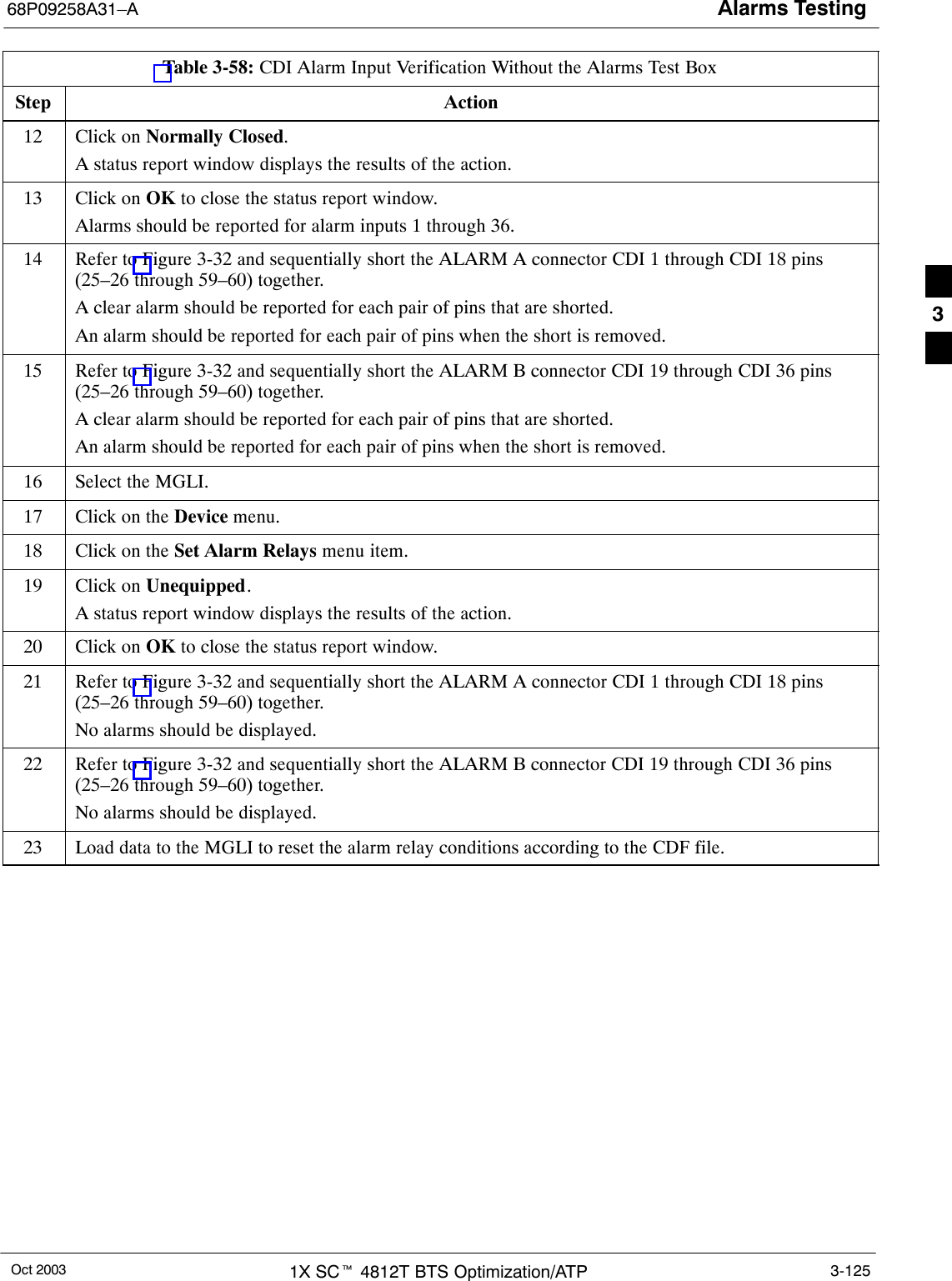
Alarms Testing68P09258A31–AOct 2003 1X SCt 4812T BTS Optimization/ATP 3-125Table 3-58: CDI Alarm Input Verification Without the Alarms Test BoxStep Action12 Click on Normally Closed.A status report window displays the results of the action.13 Click on OK to close the status report window.Alarms should be reported for alarm inputs 1 through 36.14 Refer to Figure 3-32 and sequentially short the ALARM A connector CDI 1 through CDI 18 pins(25–26 through 59–60) together.A clear alarm should be reported for each pair of pins that are shorted.An alarm should be reported for each pair of pins when the short is removed.15 Refer to Figure 3-32 and sequentially short the ALARM B connector CDI 19 through CDI 36 pins(25–26 through 59–60) together.A clear alarm should be reported for each pair of pins that are shorted.An alarm should be reported for each pair of pins when the short is removed.16 Select the MGLI.17 Click on the Device menu.18 Click on the Set Alarm Relays menu item.19 Click on Unequipped.A status report window displays the results of the action.20 Click on OK to close the status report window.21 Refer to Figure 3-32 and sequentially short the ALARM A connector CDI 1 through CDI 18 pins(25–26 through 59–60) together.No alarms should be displayed.22 Refer to Figure 3-32 and sequentially short the ALARM B connector CDI 19 through CDI 36 pins(25–26 through 59–60) together.No alarms should be displayed.23 Load data to the MGLI to reset the alarm relay conditions according to the CDF file. 3
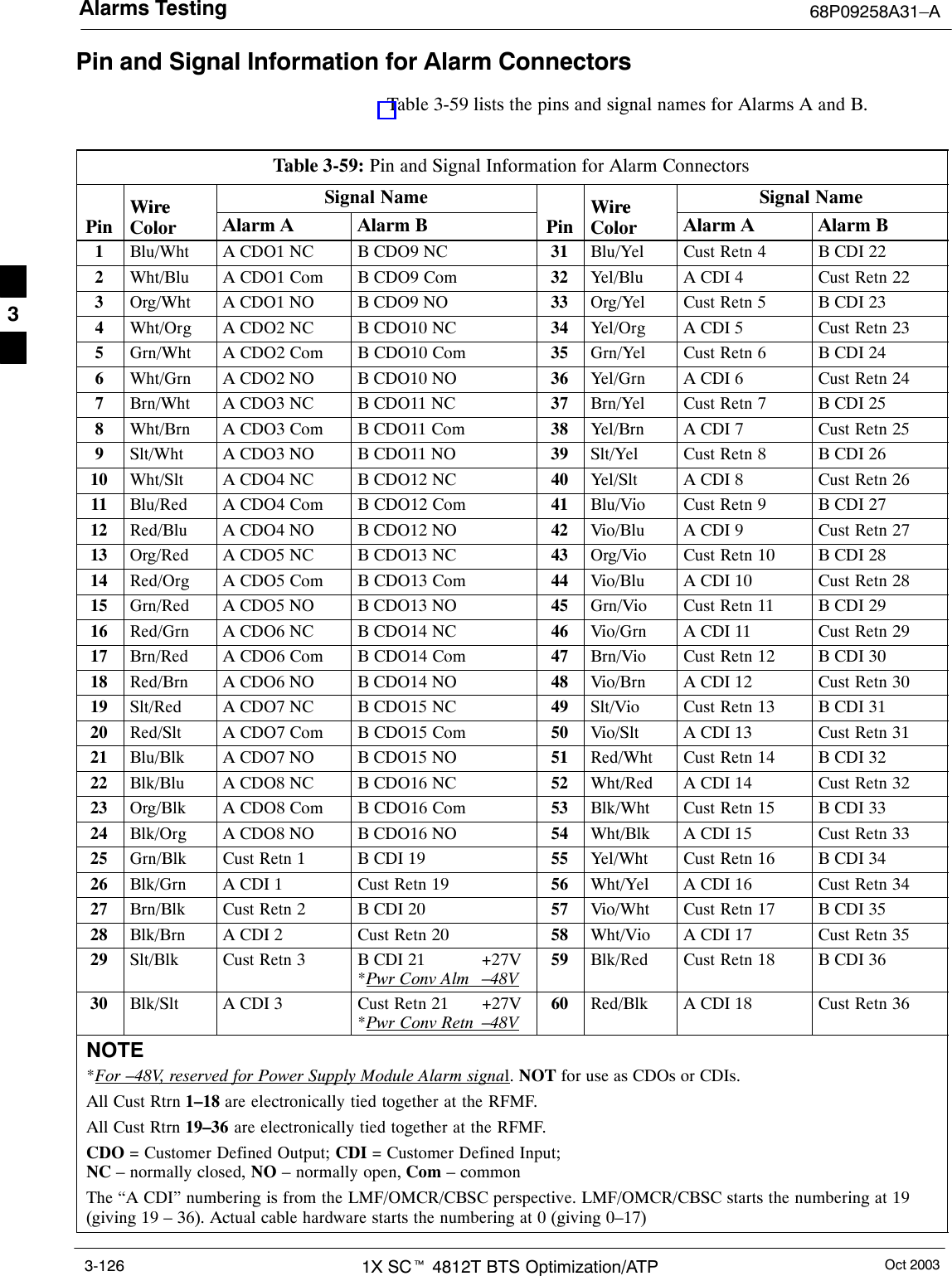
Alarms Testing 68P09258A31–AOct 20031X SCt 4812T BTS Optimization/ATP3-126Pin and Signal Information for Alarm ConnectorsTable 3-59 lists the pins and signal names for Alarms A and B.Table 3-59: Pin and Signal Information for Alarm ConnectorsWire Signal NameWireSignal NamePinWire Color Alarm A Alarm B PinWireColor Alarm A Alarm B1Blu/Wht A CDO1 NC B CDO9 NC 31 Blu/Yel Cust Retn 4 B CDI 222Wht/Blu A CDO1 Com B CDO9 Com 32 Yel/Blu A CDI 4 Cust Retn 223Org/Wht A CDO1 NO B CDO9 NO 33 Org/Yel Cust Retn 5 B CDI 234Wht/Org A CDO2 NC B CDO10 NC 34 Yel/Org A CDI 5 Cust Retn 235Grn/Wht A CDO2 Com B CDO10 Com 35 Grn/Yel Cust Retn 6 B CDI 246Wht/Grn A CDO2 NO B CDO10 NO 36 Yel/Grn A CDI 6 Cust Retn 247Brn/Wht A CDO3 NC B CDO11 NC 37 Brn/Yel Cust Retn 7 B CDI 258Wht/Brn A CDO3 Com B CDO11 Com 38 Yel/Brn A CDI 7 Cust Retn 259Slt/Wht A CDO3 NO B CDO11 NO 39 Slt/Yel Cust Retn 8 B CDI 2610 Wht/Slt A CDO4 NC B CDO12 NC 40 Yel/Slt A CDI 8 Cust Retn 2611 Blu/Red A CDO4 Com B CDO12 Com 41 Blu/Vio Cust Retn 9 B CDI 2712 Red/Blu A CDO4 NO B CDO12 NO 42 Vio/Blu A CDI 9 Cust Retn 2713 Org/Red A CDO5 NC B CDO13 NC 43 Org/Vio Cust Retn 10 B CDI 2814 Red/Org A CDO5 Com B CDO13 Com 44 Vio/Blu A CDI 10 Cust Retn 2815 Grn/Red A CDO5 NO B CDO13 NO 45 Grn/Vio Cust Retn 11 B CDI 2916 Red/Grn A CDO6 NC B CDO14 NC 46 Vio/Grn A CDI 11 Cust Retn 2917 Brn/Red A CDO6 Com B CDO14 Com 47 Brn/Vio Cust Retn 12 B CDI 3018 Red/Brn A CDO6 NO B CDO14 NO 48 Vio/Brn A CDI 12 Cust Retn 3019 Slt/Red A CDO7 NC B CDO15 NC 49 Slt/Vio Cust Retn 13 B CDI 3120 Red/Slt A CDO7 Com B CDO15 Com 50 Vio/Slt A CDI 13 Cust Retn 3121 Blu/Blk A CDO7 NO B CDO15 NO 51 Red/Wht Cust Retn 14 B CDI 3222 Blk/Blu A CDO8 NC B CDO16 NC 52 Wht/Red A CDI 14 Cust Retn 3223 Org/Blk A CDO8 Com B CDO16 Com 53 Blk/Wht Cust Retn 15 B CDI 3324 Blk/Org A CDO8 NO B CDO16 NO 54 Wht/Blk A CDI 15 Cust Retn 3325 Grn/Blk Cust Retn 1 B CDI 19 55 Yel/Wht Cust Retn 16 B CDI 3426 Blk/Grn A CDI 1 Cust Retn 19 56 Wht/Yel A CDI 16 Cust Retn 3427 Brn/Blk Cust Retn 2 B CDI 20 57 Vio/Wht Cust Retn 17 B CDI 3528 Blk/Brn A CDI 2 Cust Retn 20 58 Wht/Vio A CDI 17 Cust Retn 3529 Slt/Blk Cust Retn 3 B CDI 21  +27V*Pwr Conv Alm  –48V59 Blk/Red Cust Retn 18 B CDI 3630 Blk/Slt A CDI 3 Cust Retn 21  +27V*Pwr Conv Retn –48V60 Red/Blk A CDI 18 Cust Retn 36NOTE*For –48V, reserved for Power Supply Module Alarm signal. NOT for use as CDOs or CDIs.All Cust Rtrn 1–18 are electronically tied together at the RFMF.All Cust Rtrn 19–36 are electronically tied together at the RFMF.CDO = Customer Defined Output; CDI = Customer Defined Input; NC – normally closed, NO – normally open, Com – commonThe “A CDI” numbering is from the LMF/OMCR/CBSC perspective. LMF/OMCR/CBSC starts the numbering at 19(giving 19 – 36). Actual cable hardware starts the numbering at 0 (giving 0–17)3
Oct 2003 1X SCt 4812T BTS Optimization/ATP 4-1Chapter 4Automated Acceptance TestProcedure4
Automated Acceptance Test Procedures 68P09258A31–AOct 20031X SCt 4812T BTS Optimization/ATP4-2Automated Acceptance Test ProceduresIntroductionThe Automated Acceptance Test Procedure (ATP) allows Cellular FieldEngineers (CFEs) to run automated acceptance tests on all equipped BTSsubsystem devices using the Local Maintenance Facility (LMF) andsupported test equipment per the current Cell Site Data File (CDF)assignment.The results of these tests (at the option of the operator) are written to afile that can be printed. All tests are controlled from the LMF platformusing the GPIB interface, therefore, only recommended test equipmentsupported by the LMF can be used.This chapter describes the tests run from the GUI environment, which isthe recommended method. The GUI provides the advantages ofsimplifying the LMF user interface, reducing the potential for miskeyingcommmands and associated parameters, and speeding up the executionof complex operations involving multiple command strings. If you feelthe command line interface (CLI) will provide additional insight into theprogress of ATPs and problems that could possibly be encountered, referto LMF CLI Commands.NOTE – Before performing any tests, use an editor to view the“Caveats” section of the “readme.txt” file in the c:\wlmffolder for any applicable information.– The ATP test is to be performed on out-of-service (OOS)sectors only.– DO NOT substitute test equipment not supported by theLMF.Refer to Chapter 3 for detailed interconnection information needed forcalibrating equipment, cables, and other test equipment set components.4
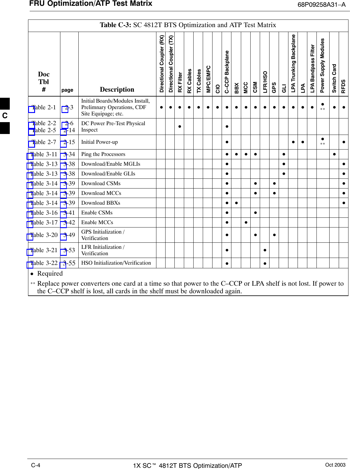
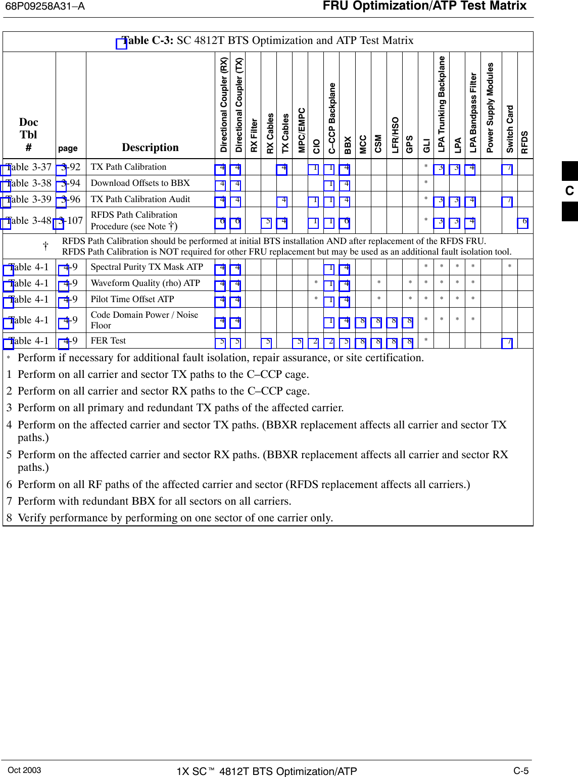
Automated Acceptance Test Procedures68P09258A31–AOct 2003 1X SCt 4812T BTS Optimization/ATP 4-3Reduced ATPNOTE Equipment has been factory–tested for FCC compliance. Iflicense–governing bodies require documentation supportingSITE compliance with regulations, a full ATP may be necessary.Perform the Reduced ATP only if reports for the specific BTSsite are NOT required.After downloading the proper operational software to the BTS, the CFEmust perform these procedures (minimal recommendation):1. Verify the TX/RX paths by performing TX Calibration, TX Audit,and FER tests.2. Retrieve Calibration Data required for normal site operation.Should failures occur while performing the specified tests, refer to theBasic Troubleshooting section of this manual for help in determining thefailure point. Once the point of failure has been identified and corrected,refer to the BTS Optimization and ATP Test Matrix (Table C-3) todetermine the applicable test that must be performed.In the unlikely event that the BTS passes these tests but has a forwardlink problem during normal operation, the CFE should then perform theadditional TX tests for troubleshooting: TX spectral mask, TX rho, andTX code domain.NOTE Refer to Chapter 3 for detailed information on test setconnections for calibrating equipment, cables and other test setcomponents, if  required.Customer requirements determine which ATP tests are to be performedand the field engineer selects the appropriate ATP tests to run.4
Automated Acceptance Test Procedures 68P09258A31–AOct 20031X SCt 4812T BTS Optimization/ATP4-4ATP Test OptionsThere are three different ATP testing options that can be performed tocompletely test a BTS. Depending on your requirements, one of thefollowing ATP testing options should be run. Table 4-1 provides theprocedure to execute an ATP test. To completely test a BTS, run the ATPtests according to one of the following ATP testing options:ATP Testing Option 1SAll TX/RX test – Executes all the TX and RX tests as described intesting option 2.ATP Testing Option 2SAll TX test – TX tests verify the performance of the BTS transmit lineup. These include the GLI, MCC, BBX, and CIO cards, the LPAs andpassive components including splitters, combiners, bandpass filter,and RF cables.SAll RX test – RX tests verify the performance of the BTS receiver lineup. These includes the MPC (for starter frames), EMPC (forexpansion frames), CIO, BBX, MCC, and GLI cards and the passivecomponents including RX filter (starter frame only), and RF cables.ATP Testing Option 3These tests can be run individually:STX Mask testSRho testSPilot Time Offset testSCode Domain Power testSFER testNOTE The Full Optimization test can be run if you want the TX pathcalibrated, BLO downloaded, and TX audited before all the TXand RX tests are run.NOTE If manual testing has been performed with the HP analyzer,remove the manual control/system memory card from the cardslot and set the IO CONFIG to the Talk & Listen mode beforestarting the automated testing.NOTE The STOP button can be used to stop the testing process.4
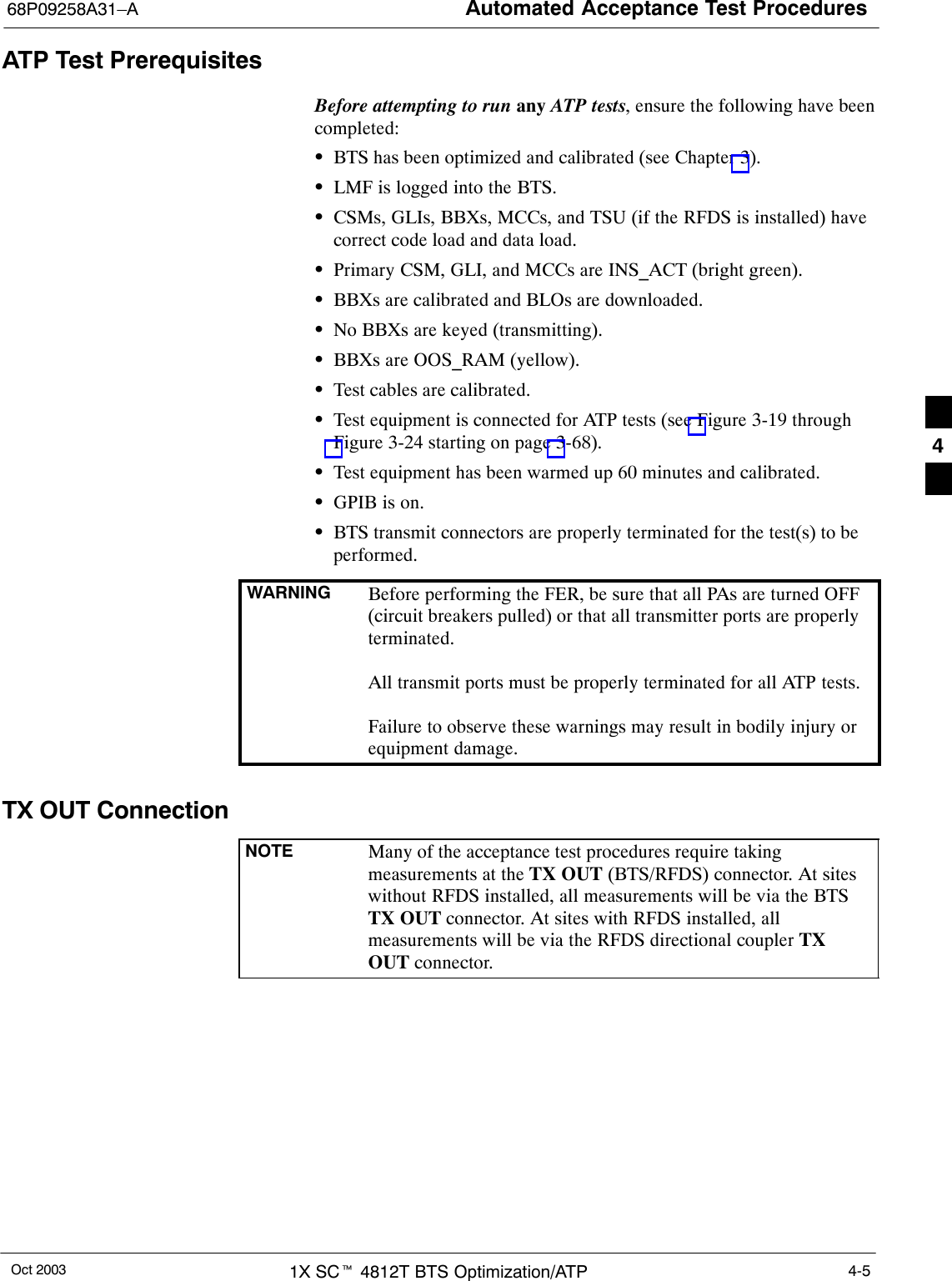
Automated Acceptance Test Procedures68P09258A31–AOct 2003 1X SCt 4812T BTS Optimization/ATP 4-5ATP Test PrerequisitesBefore attempting to run any ATP tests, ensure the following have beencompleted:SBTS has been optimized and calibrated (see Chapter 3).SLMF is logged into the BTS.SCSMs, GLIs, BBXs, MCCs, and TSU (if the RFDS is installed) havecorrect code load and data load.SPrimary CSM, GLI, and MCCs are INS_ACT (bright green).SBBXs are calibrated and BLOs are downloaded.SNo BBXs are keyed (transmitting).SBBXs are OOS_RAM (yellow).STest cables are calibrated.STest equipment is connected for ATP tests (see Figure 3-19 throughFigure 3-24 starting on page 3-68).STest equipment has been warmed up 60 minutes and calibrated.SGPIB is on.SBTS transmit connectors are properly terminated for the test(s) to beperformed.WARNING Before performing the FER, be sure that all PAs are turned OFF(circuit breakers pulled) or that all transmitter ports are properlyterminated.All transmit ports must be properly terminated for all ATP tests.Failure to observe these warnings may result in bodily injury orequipment damage.TX OUT ConnectionNOTE Many of the acceptance test procedures require takingmeasurements at the TX OUT (BTS/RFDS) connector. At siteswithout RFDS installed, all measurements will be via the BTSTX OUT connector. At sites with RFDS installed, allmeasurements will be via the RFDS directional coupler TXOUT connector.4
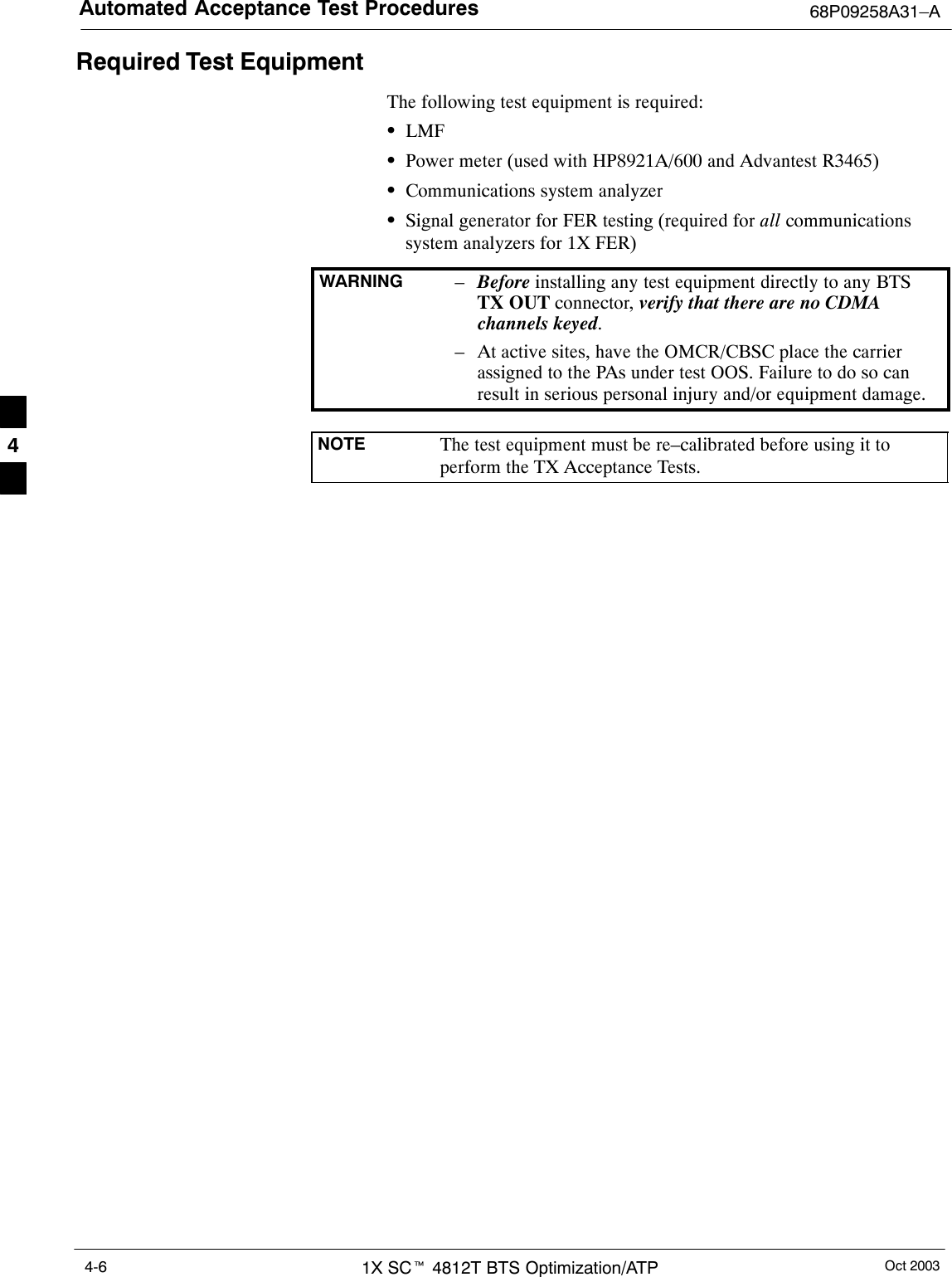
Automated Acceptance Test Procedures 68P09258A31–AOct 20031X SCt 4812T BTS Optimization/ATP4-6Required Test EquipmentThe following test equipment is required:SLMFSPower meter (used with HP8921A/600 and Advantest R3465)SCommunications system analyzerSSignal generator for FER testing (required for all communicationssystem analyzers for 1X FER)WARNING –Before installing any test equipment directly to any BTSTX OUT connector, verify that there are no CDMAchannels keyed.– At active sites, have the OMCR/CBSC place the carrierassigned to the PAs under test OOS. Failure to do so canresult in serious personal injury and/or equipment damage.NOTE The test equipment must be re–calibrated before using it toperform the TX Acceptance Tests.4
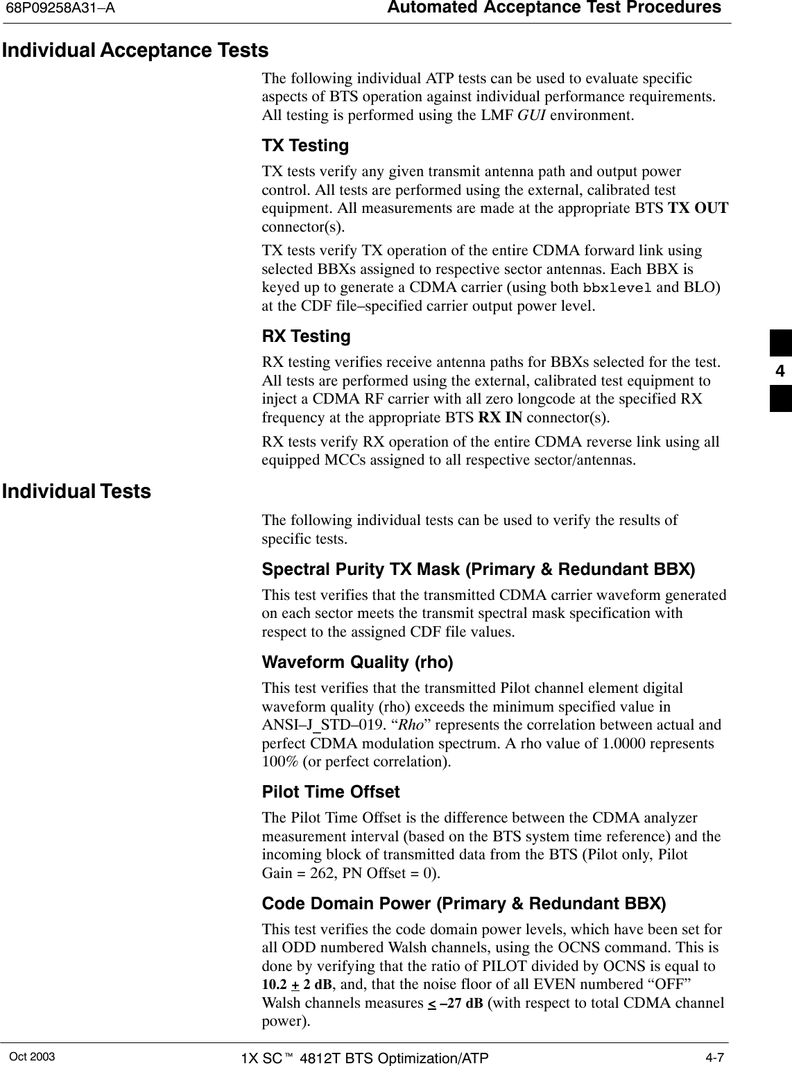
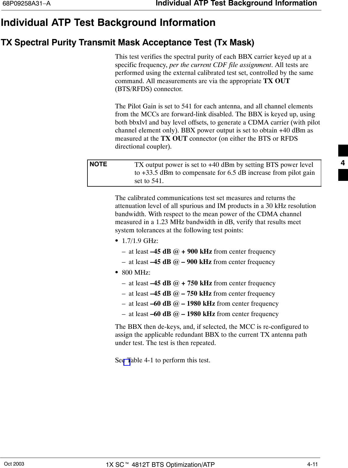
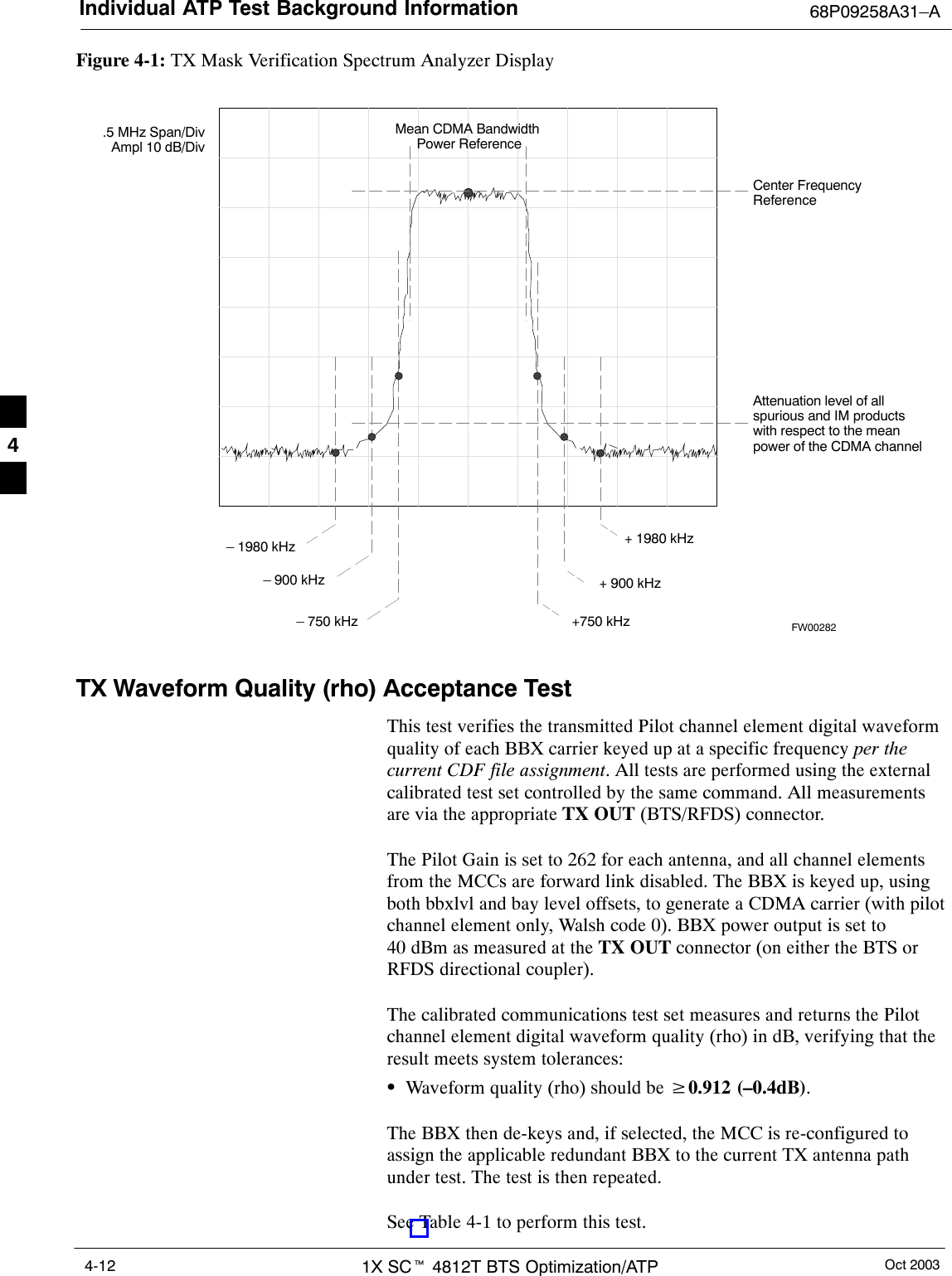
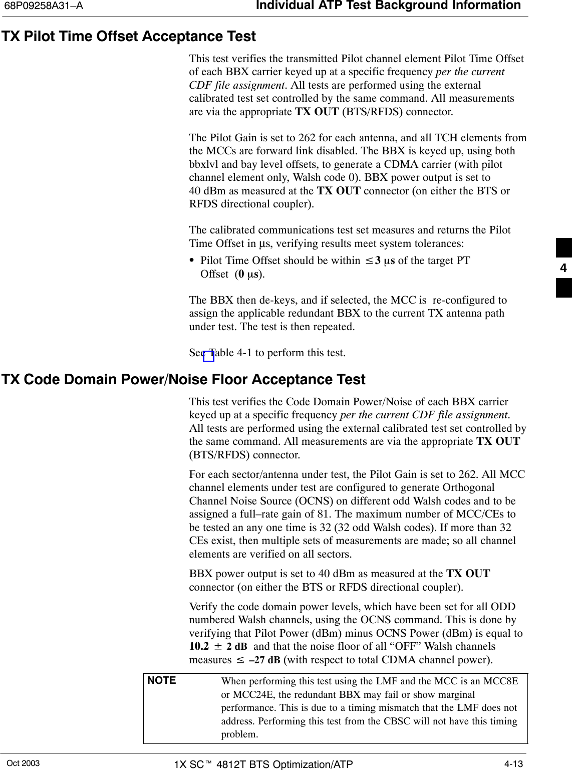
Automated Acceptance Test Procedures68P09258A31–AOct 2003 1X SCt 4812T BTS Optimization/ATP 4-7Individual Acceptance TestsThe following individual ATP tests can be used to evaluate specificaspects of BTS operation against individual performance requirements.All testing is performed using the LMF GUI environment.TX TestingTX tests verify any given transmit antenna path and output powercontrol. All tests are performed using the external, calibrated testequipment. All measurements are made at the appropriate BTS TX OUTconnector(s).TX tests verify TX operation of the entire CDMA forward link usingselected BBXs assigned to respective sector antennas. Each BBX iskeyed up to generate a CDMA carrier (using both bbxlevel and BLO)at the CDF file–specified carrier output power level.RX TestingRX testing verifies receive antenna paths for BBXs selected for the test.All tests are performed using the external, calibrated test equipment toinject a CDMA RF carrier with all zero longcode at the specified RXfrequency at the appropriate BTS RX IN connector(s).RX tests verify RX operation of the entire CDMA reverse link using allequipped MCCs assigned to all respective sector/antennas.Individual TestsThe following individual tests can be used to verify the results ofspecific tests.Spectral Purity TX Mask (Primary & Redundant BBX)This test verifies that the transmitted CDMA carrier waveform generatedon each sector meets the transmit spectral mask specification withrespect to the assigned CDF file values.Waveform Quality (rho)This test verifies that the transmitted Pilot channel element digitalwaveform quality (rho) exceeds the minimum specified value inANSI–J_STD–019. “Rho” represents the correlation between actual andperfect CDMA modulation spectrum. A rho value of 1.0000 represents100% (or perfect correlation).Pilot Time OffsetThe Pilot Time Offset is the difference between the CDMA analyzermeasurement interval (based on the BTS system time reference) and theincoming block of transmitted data from the BTS (Pilot only, PilotGain = 262, PN Offset = 0).Code Domain Power (Primary & Redundant BBX)This test verifies the code domain power levels, which have been set forall ODD numbered Walsh channels, using the OCNS command. This isdone by verifying that the ratio of PILOT divided by OCNS is equal to10.2 + 2 dB, and, that the noise floor of all EVEN numbered “OFF”Walsh channels measures < –27 dB (with respect to total CDMA channelpower).4
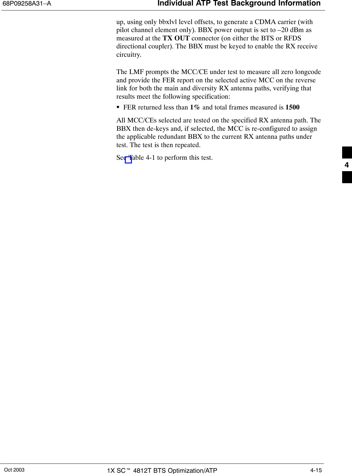
Automated Acceptance Test Procedures 68P09258A31–AOct 20031X SCt 4812T BTS Optimization/ATP4-8Frame Error RateThe Frame Error Rate (FER) test verifies RX operation of the entireCDMA Reverse Link using all equipped MCCs assigned to allrespective sectors/antennas. This test verifies the BTS sensitivity on alltraffic channel elements currently configured on all equipped MCCs atan RF input level of –119 dBm (or –116 dBm if using TMPC).4
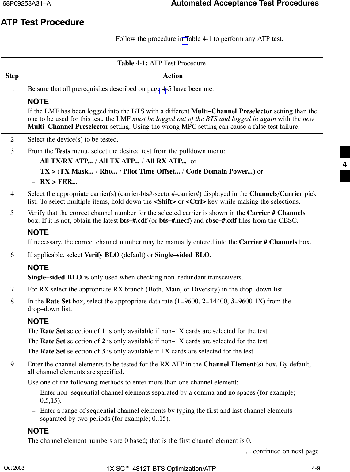
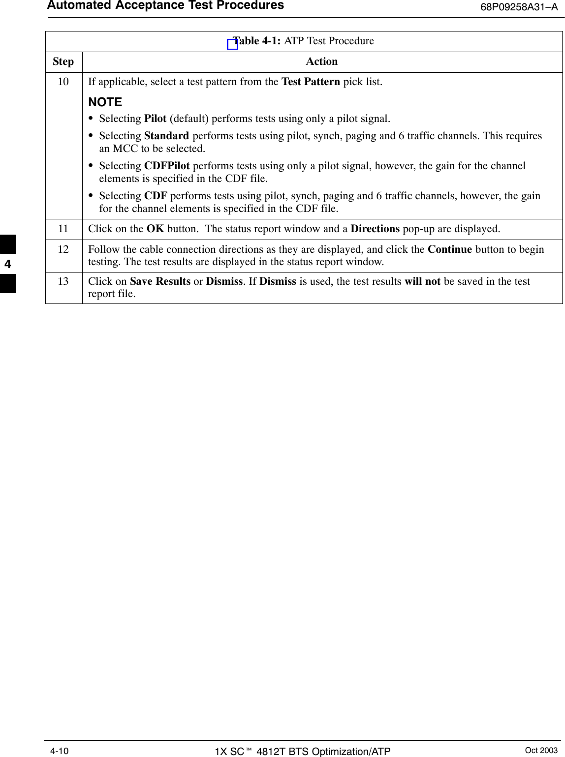
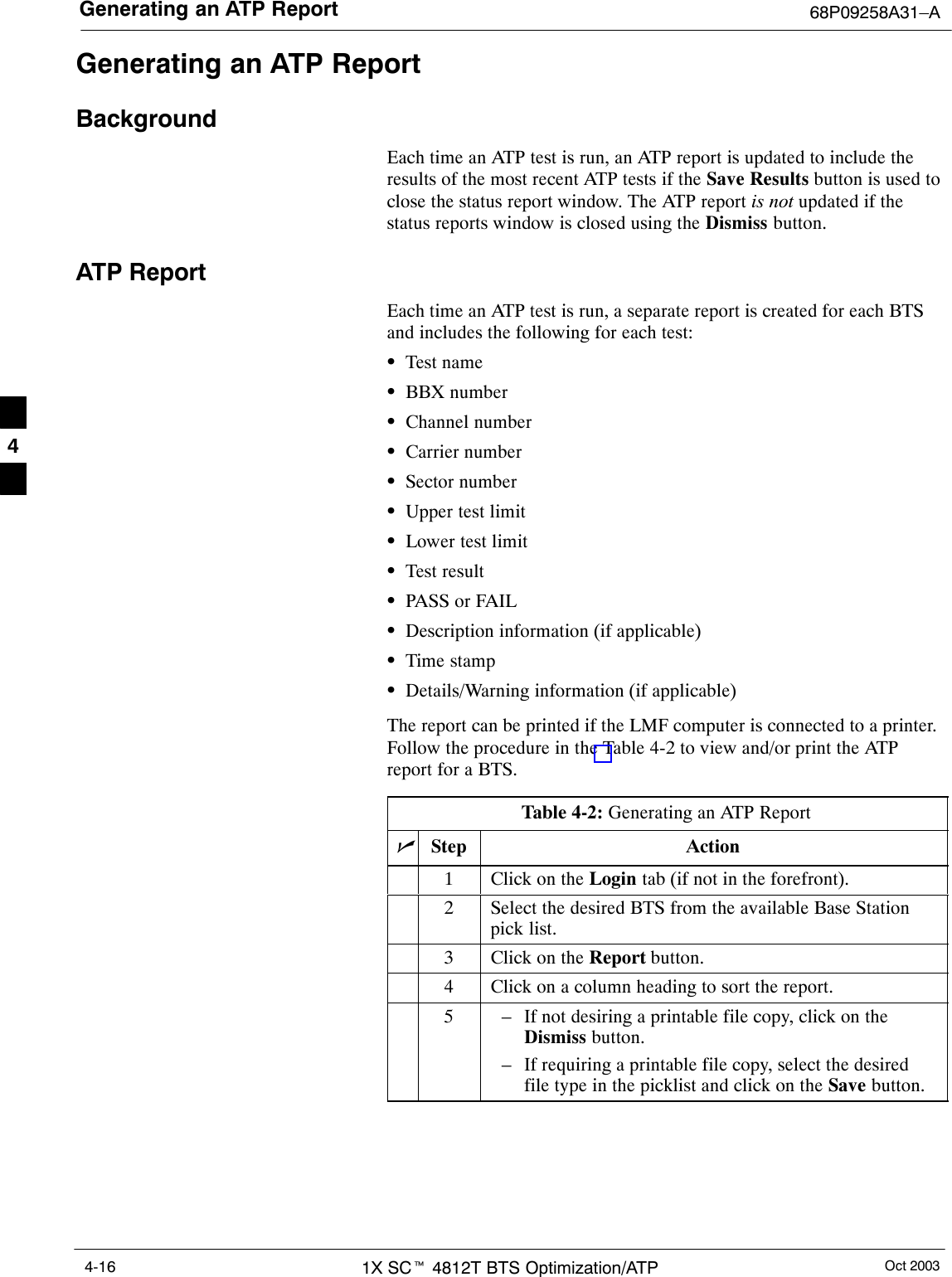
Automated Acceptance Test Procedures68P09258A31–AOct 2003 1X SCt 4812T BTS Optimization/ATP 4-9ATP Test ProcedureFollow the procedure in Table 4-1 to perform any ATP test.Table 4-1: ATP Test ProcedureStep Action 1 Be sure that all prerequisites described on page 4-5 have been met.NOTEIf the LMF has been logged into the BTS with a different Multi–Channel Preselector setting than theone to be used for this test, the LMF must be logged out of the BTS and logged in again with the newMulti–Channel Preselector setting. Using the wrong MPC setting can cause a false test failure.2Select the device(s) to be tested.3From the Tests menu, select the desired test from the pulldown menu:–All TX/RX ATP... / All TX ATP... / All RX ATP...  or –TX > (TX Mask... / Rho... / Pilot Time Offset... / Code Domain Power...) or–RX > FER...4Select the appropriate carrier(s) (carrier-bts#-sector#-carrier#) displayed in the Channels/Carrier picklist. To select multiple items, hold down the <Shift> or <Ctrl> key while making the selections.5Verify that the correct channel number for the selected carrier is shown in the Carrier # Channelsbox. If it is not, obtain the latest bts–#.cdf (or bts–#.necf) and cbsc–#.cdf files from the CBSC.NOTEIf necessary, the correct channel number may be manually entered into the Carrier # Channels box.6If applicable, select Verify BLO (default) or Single–sided BLO.NOTESingle–sided BLO is only used when checking non–redundant transceivers.7For RX select the appropriate RX branch (Both, Main, or Diversity) in the drop–down list.8In the Rate Set box, select the appropriate data rate (1=9600, 2=14400, 3=9600 1X) from thedrop–down list.NOTEThe Rate Set selection of 1 is only available if non–1X cards are selected for the test.The Rate Set selection of 2 is only available if non–1X cards are selected for the test.The Rate Set selection of 3 is only available if 1X cards are selected for the test.9Enter the channel elements to be tested for the RX ATP in the Channel Element(s) box. By default,all channel elements are specified.Use one of the following methods to enter more than one channel element:– Enter non–sequential channel elements separated by a comma and no spaces (for example;0,5,15).– Enter a range of sequential channel elements by typing the first and last channel elementsseparated by two periods (for example; 0..15).NOTEThe channel element numbers are 0 based; that is the first channel element is 0.. . . continued on next page4
Automated Acceptance Test Procedures 68P09258A31–AOct 20031X SCt 4812T BTS Optimization/ATP4-10Table 4-1: ATP Test ProcedureStep Action10 If applicable, select a test pattern from the Test Pattern pick list.NOTESSelecting Pilot (default) performs tests using only a pilot signal.SSelecting Standard performs tests using pilot, synch, paging and 6 traffic channels. This requiresan MCC to be selected.SSelecting CDFPilot performs tests using only a pilot signal, however, the gain for the channelelements is specified in the CDF file.SSelecting CDF performs tests using pilot, synch, paging and 6 traffic channels, however, the gainfor the channel elements is specified in the CDF file.11 Click on the OK button.  The status report window and a Directions pop-up are displayed.12 Follow the cable connection directions as they are displayed, and click the Continue button to begintesting. The test results are displayed in the status report window.13 Click on Save Results or Dismiss. If Dismiss is used, the test results will not be saved in the testreport file. 4
Individual ATP Test Background Information68P09258A31–AOct 2003 1X SCt 4812T BTS Optimization/ATP 4-11Individual ATP Test Background InformationTX Spectral Purity Transmit Mask Acceptance Test (Tx Mask)This test verifies the spectral purity of each BBX carrier keyed up at aspecific frequency, per the current CDF file assignment. All tests areperformed using the external calibrated test set, controlled by the samecommand. All measurements are via the appropriate TX OUT(BTS/RFDS) connector.The Pilot Gain is set to 541 for each antenna, and all channel elementsfrom the MCCs are forward-link disabled. The BBX is keyed up, usingboth bbxlvl and bay level offsets, to generate a CDMA carrier (with pilotchannel element only). BBX power output is set to obtain +40 dBm asmeasured at the TX OUT connector (on either the BTS or RFDSdirectional coupler).NOTE TX output power is set to +40 dBm by setting BTS power levelto +33.5 dBm to compensate for 6.5 dB increase from pilot gainset to 541.The calibrated communications test set measures and returns theattenuation level of all spurious and IM products in a 30 kHz resolutionbandwidth. With respect to the mean power of the CDMA channelmeasured in a 1.23 MHz bandwidth in dB, verify that results meetsystem tolerances at the following test points:S1.7/1.9 GHz:– at least –45 dB @ + 900 kHz from center frequency– at least –45 dB @ – 900 kHz from center frequencyS800 MHz:– at least –45 dB @ + 750 kHz from center frequency– at least –45 dB @ – 750 kHz from center frequency– at least –60 dB @ – 1980 kHz from center frequency– at least –60 dB @ – 1980 kHz from center frequencyThe BBX then de-keys, and, if selected, the MCC is re-configured toassign the applicable redundant BBX to the current TX antenna pathunder test. The test is then repeated.See Table 4-1 to perform this test.4
Individual ATP Test Background Information 68P09258A31–AOct 20031X SCt 4812T BTS Optimization/ATP4-12Figure 4-1: TX Mask Verification Spectrum Analyzer Display– 900 kHz + 900 kHzCenter FrequencyReferenceAttenuation level of allspurious and IM productswith respect to the meanpower of the CDMA channel.5 MHz Span/DivAmpl 10 dB/DivMean CDMA Bandwidth Power Reference+750 kHz+ 1980 kHz– 750 kHz– 1980 kHzFW00282TX Waveform Quality (rho) Acceptance TestThis test verifies the transmitted Pilot channel element digital waveformquality of each BBX carrier keyed up at a specific frequency per thecurrent CDF file assignment. All tests are performed using the externalcalibrated test set controlled by the same command. All measurementsare via the appropriate TX OUT (BTS/RFDS) connector.The Pilot Gain is set to 262 for each antenna, and all channel elementsfrom the MCCs are forward link disabled. The BBX is keyed up, usingboth bbxlvl and bay level offsets, to generate a CDMA carrier (with pilotchannel element only, Walsh code 0). BBX power output is set to40 dBm as measured at the TX OUT connector (on either the BTS orRFDS directional coupler).The calibrated communications test set measures and returns the Pilotchannel element digital waveform quality (rho) in dB, verifying that theresult meets system tolerances:SWaveform quality (rho) should be w0.912 (–0.4dB).The BBX then de-keys and, if selected, the MCC is re-configured toassign the applicable redundant BBX to the current TX antenna pathunder test. The test is then repeated.See Table 4-1 to perform this test.4
Individual ATP Test Background Information68P09258A31–AOct 2003 1X SCt 4812T BTS Optimization/ATP 4-13TX Pilot Time Offset Acceptance TestThis test verifies the transmitted Pilot channel element Pilot Time Offsetof each BBX carrier keyed up at a specific frequency per the currentCDF file assignment. All tests are performed using the externalcalibrated test set controlled by the same command. All measurementsare via the appropriate TX OUT (BTS/RFDS) connector.The Pilot Gain is set to 262 for each antenna, and all TCH elements fromthe MCCs are forward link disabled. The BBX is keyed up, using bothbbxlvl and bay level offsets, to generate a CDMA carrier (with pilotchannel element only, Walsh code 0). BBX power output is set to40 dBm as measured at the TX OUT connector (on either the BTS orRFDS directional coupler).The calibrated communications test set measures and returns the PilotTime Offset in µs, verifying results meet system tolerances:SPilot Time Offset should be within v3 ms of the target PTOffset (0ms).The BBX then de-keys, and if selected, the MCC is  re-configured toassign the applicable redundant BBX to the current TX antenna pathunder test. The test is then repeated.See Table 4-1 to perform this test.TX Code Domain Power/Noise Floor Acceptance TestThis test verifies the Code Domain Power/Noise of each BBX carrierkeyed up at a specific frequency per the current CDF file assignment.All tests are performed using the external calibrated test set controlled bythe same command. All measurements are via the appropriate TX OUT(BTS/RFDS) connector.For each sector/antenna under test, the Pilot Gain is set to 262. All MCCchannel elements under test are configured to generate OrthogonalChannel Noise Source (OCNS) on different odd Walsh codes and to beassigned a full–rate gain of 81. The maximum number of MCC/CEs tobe tested an any one time is 32 (32 odd Walsh codes). If more than 32CEs exist, then multiple sets of measurements are made; so all channelelements are verified on all sectors.BBX power output is set to 40 dBm as measured at the TX OUTconnector (on either the BTS or RFDS directional coupler).Verify the code domain power levels, which have been set for all ODDnumbered Walsh channels, using the OCNS command. This is done byverifying that Pilot Power (dBm) minus OCNS Power (dBm) is equal to10.2 $ 2 dB  and that the noise floor of all “OFF” Walsh channelsmeasures v –27 dB (with respect to total CDMA channel power).NOTE When performing this test using the LMF and the MCC is an MCC8Eor MCC24E, the redundant BBX may fail or show marginalperformance. This is due to a timing mismatch that the LMF does notaddress. Performing this test from the CBSC will not have this timingproblem.4
Individual ATP Test Background Information 68P09258A31–AOct 20031X SCt 4812T BTS Optimization/ATP4-14The BBX then de-keys and, if selected, the MCC is re-configured toassign the applicable redundant BBX to the current TX antenna pathunder test. The test is then repeated. Upon completion of the test, theOCNS is disabled on the specified MCC/CE.See Table 4-1 to perform this test.Figure 4-2: Code Domain Power and Noise Floor LevelsPilot ChannelActive channelsPILOT LEVELMAX OCNS SPEC.MIN OCNS SPEC.MAXIMUM NOISE FLOOR: < –27 dB SPEC.Inactive channelsWalsh  0  1  2   3  4  5  6   7  ... 64MAX OCNSCHANNELMIN OCNSCHANNEL8.2 dB 12.2 dBMAX NOISEFLOORPilot ChannelActive channelsPILOT LEVELMAX OCNS SPEC.MIN OCNS SPEC.MAXIMUM NOISE FLOOR:< –27 dBInactive channelsWalsh  0  1  2   3  4  5  6   7  ... 64FAILURE – DOES NOTMEET MIN OCNS SPEC.FAILURE – EXCEEDSMAX OCNS SPEC. 8.2 dB 12.2 dBFAILURE – EXCEEDS MAXNOISE FLOOR SPEC. Showing all OCNS Passing Indicating Failures FW00283RX Frame Error Rate (FER) Acceptance TestThis test verifies the BTS FER on all traffic channel elements currentlyconfigured on all equipped MCCs (full rate at 1% FER) at an RF inputlevel of –119 dBm [or –116 dBm if using Tower TopAmplifier (TMPC)]. All tests are performed using the external calibratedtest set as the signal source controlled by the same command. Allmeasurements are via the LMF.The Pilot Gain is set to 262 for each TX antenna, and all channelelements from the MCCs are forward-link disabled. The BBX is keyed4
Individual ATP Test Background Information68P09258A31–AOct 2003 1X SCt 4812T BTS Optimization/ATP 4-15up, using only bbxlvl level offsets, to generate a CDMA carrier (withpilot channel element only). BBX power output is set to –20 dBm asmeasured at the TX OUT connector (on either the BTS or RFDSdirectional coupler). The BBX must be keyed to enable the RX receivecircuitry.The LMF prompts the MCC/CE under test to measure all zero longcodeand provide the FER report on the selected active MCC on the reverselink for both the main and diversity RX antenna paths, verifying thatresults meet the following specification:SFER returned less than 1% and total frames measured is 1500All MCC/CEs selected are tested on the specified RX antenna path. TheBBX then de-keys and, if selected, the MCC is re-configured to assignthe applicable redundant BBX to the current RX antenna paths undertest. The test is then repeated.See Table 4-1 to perform this test.4
Generating an ATP Report 68P09258A31–AOct 20031X SCt 4812T BTS Optimization/ATP4-16Generating an ATP ReportBackgroundEach time an ATP test is run, an ATP report is updated to include theresults of the most recent ATP tests if the Save Results button is used toclose the status report window. The ATP report is not updated if thestatus reports window is closed using the Dismiss button.ATP ReportEach time an ATP test is run, a separate report is created for each BTSand includes the following for each test:STest nameSBBX numberSChannel numberSCarrier numberSSector numberSUpper test limitSLower test limitSTest resultSPASS or FAILSDescription information (if applicable)STime stampSDetails/Warning information (if applicable)The report can be printed if the LMF computer is connected to a printer.Follow the procedure in the Table 4-2 to view and/or print the ATPreport for a BTS.Table 4-2: Generating an ATP ReportnStep Action1Click on the Login tab (if not in the forefront).2Select the desired BTS from the available Base Stationpick list.3Click on the Report button.4Click on a column heading to sort the report.5– If not desiring a printable file copy, click on theDismiss button.– If requiring a printable file copy, select the desiredfile type in the picklist and click on the Save button.4
Oct 2003 1X SCt 4812T BTS Optimization/ATP 5-1Chapter 5Prepare to Leave the Site5
Updating Calibration Data Files 68P09258A31–AOct 20031X SCt 4812T BTS Optimization/ATP5-2Updating Calibration Data FilesSoftware Release caveatsWith Software Release 2.16.1.x, the packet BTS will NOT detect a newcalibration file on the OMC–R. A manual workaround is available inbulletin cdma_g_bts_059. This will be corrected in Software Release2.16.3.Software Release 2.16.3 will allow the user to load the calibration filefrom the LMF directly onto the MGLI. The MGLI will then ftp the newcalibration file to the OMC–R, thereby eliminating the need for the userto place the calibration file at the OMC–R.Copy and Load Cal File to to CBSCAfter completing the TX calibration and audit, updated CAL fileinformation must be moved from the LMF Windows environment backto the CBSC, a Unix environment. The following procedures detailmoving files from one environment to the other.Copying CAL files from LMF to a DisketteFollow the procedures in Table 5-1 to copy the CAL files from an LMFcomputer to a 3.5 diskette.Table 5-1: Copying CAL Files to a DisketteStep Action1 With Windows running on the LMF computer, insert a disk into Drive A:\.2Launch the Windows Explorer application program from the Start > Programs menu list.3Select the applicable <x>:\<lmf home directory/cdma/bts–# folder.4Drag the bts–#.cal file to Drive A.5Repeat Steps 3 and 4, as required, for other bts–# folders. 5
Updating Calibration Data Files68P09258A31–AOct 2003 1X SCt 4812T BTS Optimization/ATP 5-3Copying CAL Files from Diskette to the CBSCFollow the procedure in Table 5-2 to copy CAL files from a diskette tothe CBSC.Table 5-2: Procedures to Copy CAL Files from Diskette to the CBSCStep Action1Log into the CBSC on the OMC–R Unix workstation using your account name and password.2Place the diskette containing calibration files (cal files) in the workstation diskette drive.3 Type eject –q and press the Enter key.4 Type mount and press the Enter key. Verify that floppy/no_name  is displayed.NOTEIf the eject command has been previously entered, floppy/no_name  will be appended with anumber. Use the explicit floppy/no_name  reference displayed.5Type in cd /floppy/no_name and press the Enter key.6Type in ls –lia and press the Enter key. Verify the bts–#.cal file filename appears in the displayeddirectory listing.7Type in cd and press the Enter key.8Type in pwd and press the Enter key. Verify the displayed response shows the correct home directory(/home/<user’s name>).9 With Solaris versions of Unix, create a Unix–formatted version of the bts–#.cal file in the homedirectory by performing the following:9a – Type in dos2unix  /floppy/no_name/bts–#.cal  bts–#.cal and press the Enter key.Where:  #  =  BTS number for which the CAL file was createdNOTEOther versions of Unix do not support the dos2unix command. In these cases, use the Unix cp (copy)command. The copied files will contain DOS line feed characters which must be edited out with aUnix text editor.10 Type in ls –l *.cal and press the Enter key. Verify the CAL files have been copied. Verify all CALfiles to be transferred appear in the displayed listing.11 Type eject and press the Enter key.12 Remove the diskette from the workstation. 5
Prepare to Leave the Site 68P09258A31–AOct 20031X SCt 4812T BTS Optimization/ATP5-4Prepare to Leave the SiteExternal Test Equipment RemovalPerform the procedure in Table 5-3 to disconnect the test equipment andconfigure the BTS for active service.Table 5-3: External Test Equipment RemovalStep Action1Disconnect all external test equipment from all TX and RXconnectors on the top of the frame.2Reconnect and visually inspect all TX and RX antenna feedlines at the top of the frame.CAUTION Verify that all sector antenna feed lines are connected to thecorrect ports on the frame. Crossed antenna cables will causesystem degradation of call processing.NOTE Each module or device can be in any state prior to downloading.Each module or device will be in an OOS_RAM state afterdownloading has completed.– For all LMF commands, information in italics representsvalid ranges for that command field.– Only those fields requiring an input will be specified.Default values for other fields will be assumed.– For more complete command examples (including systemresponse details), refer to the CDMA LMF User  Guide.5
Prepare to Leave the Site68P09258A31–AOct 2003 1X SCt 4812T BTS Optimization/ATP 5-5BTS Site Span Configuration VerificationTable 5-4 describes how to verify the current Span Framing Format andLine Build Out (LBO) parameters. ALL MGLI2/GLI2 boards in allC–CCP shelves that terminate a T1/E1 span should be verified.Table 5-4: BTS Span Parameter ConfigurationStep Action1Connect a serial cable from the LMF COM1 port (via null modem board) to the front panel of theMGLI2 MMI port (see Figure 5-1).2Start an MMI communication session with MGLI2 by using the Windows desktop shortcut icon (seeTable 3-3 on page 3-13).NOTEThe LMF program must not be running when a Hyperterminal session is started if COM1 is beingused for the MMI session.3Enter the following MMI command to display the current MGLI2/GLI2 framing format and line codeconfiguration (in bold type):span view <cr>Observe a display similar to the options shown below:COMMAND ACCEPTED: span viewThe parameter in NVM is set to T1_2.The frame format in flash is set to use T1_2.Equalization:  Span A – Default (0–131 feet for T1/J1, 120 Ohm for E1)  Span B – Default (0–131 feet for T1/J1, 120 Ohm for E1)  Span C – Default (0–131 feet for T1/J1, 120 Ohm for E1)  Span D – Default (0–131 feet for T1/J1, 120 Ohm for E1)  Span E – Default (0–131 feet for T1/J1, 120 Ohm for E1)  Span F – Default (0–131 feet for T1/J1, 120 Ohm for E1)Linkspeed: Default (56K for T1 D4 AMI, 64K otherwise)Currently, the link is running at the default rate The actual rate is 0Clock Alarms (0000):DPLL is locked and has a reference source.GPS receiver self test result: passedTime since reset 0:33:11, time since power on: 0:33:11 . . . . . . . . . . . . . . . . . . . . . . . . . . . . . . . . . . 3-40 NOTE– Defaults for span equalization are 0–131 feet for T1/J1 spans and 120 Ohm for E1.– Default linkspeed is 56K for T1 D4 AMI spans and 64K for all other types.– There is no need to change from defaults unless the OMC–R/CBSC span configuration requires it.– If the current MGLI2/GLI2 framing format and line code configuration does not display thecorrect choice, proceed to Table 5-5.4Repeat steps 1 through 3 for all remaining GLIs.5Exit the GLI MMI session and HyperTerminal connection by selecting File from the connectionwindow menu bar, and then Exit from the drop–down menu. 5
Prepare to Leave the Site 68P09258A31–AOct 20031X SCt 4812T BTS Optimization/ATP5-6Figure 5-1: MGLI2/GLI2 MMI Port ConnectionFW003449–PIN TO 9– PINRS–232 CABLENULL MODEM BOARD(PART# 8484877P01)RS–232 CABLE FROM LMF COM1PORTMMI SERIAL PORTGLI BOARDSet BTS Site Span ConfigurationPerform the procedure in Table 5-5 to configure the Span FramingFormat and Line Build Out (LBO) parameters. ALL MGLI2/GLI2boards in all C–CCP shelves that terminate a T1/E1 span must beconfigured.NOTE Perform the following procedure ONLY if span configurationsloaded in the MGLI2/GLI2s do not match those in theOMCR/CBSC data base, AND ONLY when the exactconfiguration data is available. Loading incorrect spanconfiguration data will render the site inoperable.Table 5-5: Set BTS Span Parameter ConfigurationStep Action1If not already done, connect a serial cable from the LMF COM1 port (via null modem board) to thefront panel of the MGLI2 MMI port (see Figure 5-1).2Start an MMI communication session with CSM–1 by using the Windows desktop shortcut icon (seeTable 3-3 on page 3-13).NOTEThe LMF program must not be running when a Hyperterminal session is started if COM1 is beingused for the MMI session.. . . continued on next page5
Prepare to Leave the Site68P09258A31–AOct 2003 1X SCt 4812T BTS Optimization/ATP 5-7Table 5-5: Set BTS Span Parameter ConfigurationStep Action3If required only, enter the following MMI command for each span line to set the BTS span parametersto match that of the physical spans a – f run to the site:span_config <option#1> <option#2>  <option#3> <option#4> <option#5>option#1  =  the span to change (a – f)option#2  =  the span type (0 – 8):0 – E1_1 (HDB3, CCS, CRC–4)1 – E1_2 (HDB3, CCS)2 – E1_3 (HDB3, CAS, CRC–4, TS16)3 – E1_4 (HDB3, CAS, TS16)4 – T1_1 (AMI, DS1 AT&T D4, without ZCS, 3 to 1 packing, Group 0 unusable)5 – T1_2 (B8ZS, DS1 AT&T ESF, 4 to 1 packing, 64K link)6 – J1_1 (B8ZS, J1 AT&T ESF, Japan CRC6, 4 to 1 packing)7 – J1_2 (B8ZS, J1 AT&T ESF, US CRC6, 4 to 1 packing)8 – T1_3 (AMI, DS1 AT&T D4, with ZCS, 3 to 1 packing, Group 0 unusable)option#3  =  the link speed (56 or 64) Kbpsoption#4  =  the span equalization (0 – 7):0 – T1_6 (T1,J1:long haul)1 – T1_4 (T1,J1:393–524 feet)2 – T1_4 (T1,J1:131–262 feet)3 – E1_75 (E1:75 Ohm)4 – T1_4 (T1,J1:0–131 feet)5 – T1_4 (T1,J1:524–655 feet)6 – T1_4 (T1,J1:262–393 feet)7 – E1_120 (E1:120 Ohm)option#5  =  the slot that has LAPD channel (0 – 31)Example for setting span configuration to E1_2, 64 Kbps, E1_120–Ohm, LAPD channel 1:span_config  a 1 64 7 1..span_config f 1 64 7 1Example for setting span configuration to T1_2, 64 Kbps, T1_4 (0–131 feet), LAPD channel 0:span_config  a 5 64 4 0..span_config f 5 64 4 0NOTEMake sure that spans a – f are set to the same span type and link speed. The equalization may bedifferent for each individual span.After executing the span_config command, the affected MGLI2/GLI2 board MUST be reset andre–loaded for changes to take effect.Although defaults are shown, always consult site specific documentation for span type and rate used atthe site.4Press the RESET button on the GLI2 for changes to take effect.. . . continued on next page5
Prepare to Leave the Site 68P09258A31–AOct 20031X SCt 4812T BTS Optimization/ATP5-8Table 5-5: Set BTS Span Parameter ConfigurationStep Action5This completes the site specific BTS Span setup for this GLI. Move the MMI cable to the next GLI2and repeat steps 1 and 4 for ALL MGLI2/GLI2 boards.6Terminate the Hyperterm session and disconnect the LMF from the MGLI/SGLI. LMF RemovalPerform the procedure in Table 5-6 as required to terminate the LMFGUI session and remove the LMF computer.Table 5-6: Terminate the LMF Session and Remove the LMFStep Action! CAUTIONDO NOT power down the CDMA LMF without performing the procedure indicated below.Corrupted/lost data files may result, and in some cases, the CDMA LMF may lock up.1Log out of all BTS sessions and exit LMF by clicking on File in the LMF window menu bar and selectingLogout and Exit from the pull–down list.2From the Windows Task Bar click Start>Shutdown. Click Yes when the Shut Down Windowsmessage appears.3Wait for the system to shut down and the screen to go blank.4Disconnect the LMF terminal Ethernet connector from the BTS cabinet.5Disconnect the LMF serial port, the RS-232 to GPIB interface box, and the GPIB cables as requiredfor equipment transport.5
Prepare to Leave the Site68P09258A31–AOct 2003 1X SCt 4812T BTS Optimization/ATP 5-9Re–connect BTS T1/E1 Spans and Integrated Frame ModemBefore leaving the site, connect any T1 span TELCO connectors thatwere removed to allow the LMF to control the BTS. Refer to Table 5-7and Figure 5-2 as required.Table 5-7: T1/E1 Span/IFM ConnectionsStep Action1Connect the 50–pin TELCO cables to the BTS span I/O board 50–pin TELCO connectors.2If used, connect the dial–up modem RS–232 serial cable to the Site I/O board RS–232 9–pinsub D connector.NOTEVerify that you connect both SPAN cables (if removed previously), and the Integrated FrameModem (IFM) “TELCO” connector.Figure 5-2: Site and Span I/O Boards T1 Span Connections50–PIN TELCOCONNECTORSREMOVEDSPAN A CONNECTOR(TELCO) INTERFACETO SPAN LINESSPAN B CONNECTOR(TELCO) INTERFACETO SPAN LINESTOP of Frame (Site I/O and Span I/O boards)RS–232 9–PIN SUB DCONNECTOR SERIALPORT FOR EXTERNALDIAL UP MODEMCONNECTION (IF USED)FW002995
Prepare to Leave the Site 68P09258A31–AOct 20031X SCt 4812T BTS Optimization/ATP5-10Reset All Devices and Initialize Site RemotelyDevices in the BTS should not be left with data and code loaded fromthe LMF. The configuration data and code loads used for normaloperation could be different from those stored in the LMF files. Performthe procedure in Table 5-8 to reset all devices and initialize site remotely.Table 5-8: Reset BTS Devices and Remote Site InitializationStep Action1Terminate the LMF session by following the procedures in Table 5-6.2Reconnect spans by following the procedure in Table 5-7.3– If BTS is configured for circuit operation, go to Step 4.– If BTS is configured for packet operation, go to Step 5.4Circuit BTS Procedure:4a From the BTS site, contact the OMC–R and request the operator to perform a BTS reset.orAt the BTS site:– unseat one GLI card at a time and wait for 30 seconds;– reseat the GLI and wait for it to complete its initialization (this takes about one minute);– repeat for the second GLI.4b Depending on the number of installed operational GLI cards, perform one of the following:– With fully redundant GLIs, contact the OMC–R and request the operator to run the ACTIVATEcommand for the BTS.– For a non–redundant GLI or a frame where the redundant GLI is not operational, contact theOMC–R and request the operator:SACTIVATE the GLI to set the Nextload attribute for the GLI to the one for the current BSSsoftware version;SDisable the GLI;SEnable the GLI to allow the MM to load the software version specified by the Nextloadattribute;SOnce the GLI is INS_ACT, contact the OMC–R and request the operator ACTIVATE the BTS.– Once the GLI cards are loaded with the specified code version, the active GLI will verify andupdate, as required, the RAM and, if it is necessary, ROM code loads for the installed CSM,MCC, and BBX cards using the DLM.. . . continued on next page5
Prepare to Leave the Site68P09258A31–AOct 2003 1X SCt 4812T BTS Optimization/ATP 5-11Table 5-8: Reset BTS Devices and Remote Site InitializationStep Action5Packet BTS procedure:5a From the BTS site, contact the OMC–R and request the operator to PREACTIVATE the BTS to therequired software version for the BSS. There are two types of PREACTIVATE load processes:–Rolling Upgrade: This load process is only available when the BTS cards are populated for fullredundancy as applicable.–Quick Reboot: This process is used when there is not full redundancy for the BTS cards. TheGLI3 will disable and reboot to the new load. This will cause all the other cards to go out ofservice. Once it is rebooted, the GLI3 determines which cards require a new load and thendownloads the cards in the order which they establish communication with the GLI3 followingtheir reboot. The GLI3 can reload up to 16 devices simultaneously.6After all activities at the site have been completed, contact the OMC–R and confirm that the BTS isunder OMC–R control. 5
Prepare to Leave the Site 68P09258A31–AOct 20031X SCt 4812T BTS Optimization/ATP5-12Notes5
Oct 2003 1X SCt 4812T BTS Optimization/ATP 6-1Chapter 6Basic Troubleshooting6
Basic Troubleshooting Overview 68P09258A31–AOct 20031X SCt 4812T BTS Optimization/ATP6-2Basic Troubleshooting OverviewOverviewThe information in this section addresses some of the scenarios likely tobe encountered by Cellular Field Engineering (CFE) team members.This troubleshooting guide was created as an interim reference documentfor use in the field. It provides basic “what to do if” basictroubleshooting suggestions when the BTS equipment does not performper the procedure documented in the manual.Comments are consolidated from inputs provided by CFEs in the fieldand information gained form experience in Motorola labs andclassrooms.6
Troubleshooting: Installation68P09258A31–AOct 2003 1X SCt 4812T BTS Optimization/ATP 6-3Troubleshooting: InstallationCannot Log into Cell-SiteFollow the procedure in Table 6-1 to troubleshoot a login failure.Table 6-1: Login Failure Troubleshooting ProceduresnStep Action1If the MGLI LED is solid RED, it implies a hardware failure. Reset the MGLI by re-seating it. Ifthis persists, install a known good MGLI card in the MGLI slot and retry. A Red LED may alsoindicate no Ethernet termination at top of frame.2Verify that T1 is disconnected (see Table 3-4 on page 3-16).If T1 is still connected, verify the CBSC has disabled the BTS.3Try pinging the MGLI (see Table 3-11 on page 3-34).4Verify the LMF is connected to the Primary LMF port (LAN A) in the front of the BTS (seeTable 3-5 on page 3-17).5Verify the LMF was configured properly (see Preparing the LMF section starting on page 3–6).6Verify the BTS-LMF cable is RG-58 [flexible black cable of less than 76 cm (2.5 feet) length].7Verify the Ethernet ports are terminated properly (see Figure 3-9 on page 3-33).8Verify a T-adapter is not used on the LMF side port if connected to the BTS front LMF primaryport.9Try connecting to the I/O panel (top of frame). Use BNC T-adapters at the LMF port for thisconnection.10 Re-boot the LMF and retry.11 Re-seat the MGLI and retry.12 Verify IP addresses are configured properly.Cannot Communicate to Power MeterFollow the procedure in Table 6-2 to troubleshoot a power metercommunication failure.Table 6-2:  Troubleshooting a Power Meter Communication FailurenStep Action1Verify the Power Meter is connected to the LMF with a GPIB adapter.2Verify the cable setup as specified in Chapter 3.3Verify the GPIB address of the power meter is set to the same value displayed in the applicableGPIB address box of the LMF Options window Test Equipment tab. Refer to Table 3-25 orTable 3-26 and the GPIB Addresses section of Appendix F for details.4Verify the GPIB adapter DIP switch settings are correct. Refer to the CDMA 2000 Test EquipmentPreparation section of Appendix F for details.. . . continued on next page6
Troubleshooting: Installation 68P09258A31–AOct 20031X SCt 4812T BTS Optimization/ATP6-4Table 6-2:  Troubleshooting a Power Meter Communication FailurenActionStep5Verify the GPIB adapter is not locked up. Under normal conditions, only two green LEDs must be‘ON’ (Power and Ready). If any other LED is continuously ‘ON’, then cycle GPIB box power andretry.6Verify the LMF computer COM1 port is not used by another application; for example, if aHyperTerminal window is open for MMI, close it.7Reset all test equipment by clicking Util in the BTS menu bar and selectingTest Equipment>Reset from the pull–down lists. Cannot Communicate to Communications AnalyzerFollow the procedure in Table 6-3 to troubleshoot a communicationsanalyzer communication failure.Table 6-3:  Troubleshooting a Communications Analyzer Communication FailurenStep Action1Verify signal generator is connected to LMF with GPIB adapter.2Verify cable connections as specified in Chapter 3.3Verify the signal generator GPIB address is set to the same value displayed in the applicable GPIBaddress box of the LMF Options window Test Equipment tab. Refer to Table 3-25 or Table 3-26and the GPIB Address section of Appendix F for details.4Verify the GPIB adapter DIP switch settings are correct. Refer to the CDMA 2000 Test EquipmentPreparation section of Appendix F for details.5Verify the GPIB adapter is not locked up. Under normal conditions, only two green LEDs must be‘ON’ (Power and Ready). If any other LED is continuously ‘ON’, then cycle the GPIB box powerand retry.6Verify the LMF computer COM1 port is not used by another application; for example, if aHyperTerminal window is open for MMI, close it.7 Reset all test equipment by clicking Util in the BTS menu bar and selectingTest Equipment>Reset from the pull–down lists.6
Troubleshooting: Download68P09258A31–AOct 2003 1X SCt 4812T BTS Optimization/ATP 6-5Troubleshooting: DownloadCannot Download CODE to Any Device (card)Follow the procedure in Table 6-4 to troubleshoot a code downloadfailure.Table 6-4: Troubleshooting Code Download FailurenStep Action1Verify T1 is disconnected from the BTS.2Verify the LMF can communicate with the BTS device using the Status function.3Communication to the MGLI must first be established before trying to talk to any other BTSdevice.The MGLI must be INS_ACT state (green).4Verify the card is physically present in the cage and powered-up.5If the card LED is solid RED, it implies hardware failure.Reset the card by re-seating it.If the LED remains solid red, replace with a card from another slot & retry.NOTEThe card can only be replaced by a card of the same type.6Re-seat the card and try again.7If a BBX reports a failure message and is OOS_RAM, the code load was OK. Use the LMFStatus function to verify the load.8If the download portion completes and the reset portion fails, reset the device by selecting thedevice and Reset.9If a BBX or an MCC remains OOS_ROM (blue) after code download, use the LMFDevice > Status function to verify that the code load was accepted.10 If the code load was accepted, use LMF Device > Download > Flash to load RAM code into flashmemory.Cannot Download DATA to Any Device (Card)Perform the procedure in Table 6-5 to troubleshoot a data downloadfailure.Table 6-5: Troubleshooting Data Download FailurenStep Action1Re-seat the card and repeat code and data load procedure.6
Troubleshooting: Download 68P09258A31–AOct 20031X SCt 4812T BTS Optimization/ATP6-6Cannot ENABLE DeviceBefore a device can be enabled (placed in-service), it must be in theOOS_RAM state (yellow) with data downloaded to the device. The colorof the device changes to green once it is enabled.The three states that devices can be changed to are as follows:SEnabled (green, INS)SDisabled (yellow, OOS_RAM)SReset (blue, OOS_ROM)Follow the procedure in Table 6-6 to troubleshoot a device enablefailure.Table 6-6: Troubleshooting Device Enable (INS) FailurenStep Action1Re-seat the card and repeat the code and data load procedure.2If the CSM cannot be enabled, verify the CDF file has correct latitude and longitude data for cellsite location and GPS sync.3Ensure the primary CSM is in INS_ACT state.NOTEMCCs will not go INS without the CSM being INS.4Verify the 19.6608 MHz CSM clock; MCCs will not go INS otherwise.5The BBX should not be enabled for ATP tests.6If MCCs give “invalid or no system time”, verify the CSM is operable. Miscellaneous ErrorsPerform the procedure in Table 6-7 to troubleshoot miscellaneousfailures.Table 6-7: Miscellaneous FailuresnStep Action1If LPAs continue to give alarms, even after cycling power at the circuit breakers, then connect anMMI cable to the LPA and set up a Hyperterminal connection (see Table 3-3 on page 3-13).2 Enter ALARMS in the Hyperterminal window.The resulting LMF display may provide an indication of the problem.(Call Field Support for further assistance.)6
Troubleshooting: Calibration68P09258A31–AOct 2003 1X SCt 4812T BTS Optimization/ATP 6-7Troubleshooting: CalibrationBay Level Offset Calibration FailurePerform the procedure in Table 6-8 to troubleshoot a BLO calibrationfailure.Table 6-8: Troubleshooting BLO Calibration FailurenStep Action1Verify the Power Meter is configured correctly (see the test equipment setup section in Chapter 3)and connection is made to the proper TX port.2Verify the parameters in the bts–#.cdf file are set correctly for the following bands:For 1900 MHz:Bandclass=1; Freq_Band=16; SSType=16For 800 MHz:Bandclass=0; Freq_Band=8; SSType=8For 1700 MHz:Bandclass=4; Freq_Band=128; SSType=163Verify that no LPA in the sector is in alarm state (flashing red LED).Reset the LPA by pulling the circuit breaker and, after 5 seconds, pushing back in.4Re-calibrate the Power Meter and verify it is calibrated correctly with cal factors from the sensorhead.5Verify the GPIB adapter is not locked up.Under normal conditions, only two green LEDs must be ‘ON’ (Power and Ready).If any other LED is continuously ‘ON’, power-cycle (turn power off and on) the GPIB Box andretry.6Verify the sensor head is functioning properly by checking it with the 1 mW (0 dBm) Power Refsignal.7If communication between the LMF and Power Meter is operational, the Meter display will show“RES”. 6
Troubleshooting: Calibration 68P09258A31–AOct 20031X SCt 4812T BTS Optimization/ATP6-8Cannot Load BLOFor Load BLO failures see Table 6-7.Calibration Audit FailureFollow the procedure in Table 6-9 to troubleshoot a calibration auditfailure.Table 6-9: Troubleshooting Calibration Audit FailurenStep Action1Verify the Power Meter is configured correctly (refer to the test equipment setup section ofChapter  3).2Re-calibrate the Power Meter and verify it is calibrated correctly with cal factors from the sensorhead.3Verify that no LPA is in alarm state (rapidly flashing red LED).Reset the LPA by pulling the circuit breaker and, after 5 seconds, pushing back in.4Verify that no sensor head is functioning properly by checking it with the 1 mW (0 dBm) PowerRef signal.5After calibration, the BLO data must be re-loaded to the BBXs before auditing.Click on the BBX(s) and select Device>Download BLO.Re-try the audit.6Verify the GPIB adapter is not locked up.Under normal conditions, only two green LEDs must be “ON” (Power and Ready).If any other LED is continuously “ON”, power-cycle (turn power off and on) the GPIB Box andretry. 6
Troubleshooting: Transmit ATP68P09258A31–AOct 2003 1X SCt 4812T BTS Optimization/ATP 6-9Troubleshooting: Transmit ATPBTS passed Reduced ATP tests but has forward link problem during normaloperationFollow the procedure in Table 6-10 to troubleshoot a Forward Linkproblem during normal operation.Table 6-10: Troubleshooting Forward Link Failure (BTS Passed Reduced ATP)nStep Action1Perform these additional TX tests to troubleshoot a forward link problem:– TX mask– TX rho– TX code domainCannot Perform TX Mask MeasurementFollow the procedure in Table 6-11 to troubleshoot a TX maskmeasurement failure.Table 6-11: Troubleshooting TX Mask Measurement FailurenStep Action1Verify that TX audit passes for the BBX(s).2If performing manual measurement, verify analyzer setup.3Verify that no LPA in the sector is in alarm state (flashing red LED).Re-set the LPA by pulling the circuit breaker and, after 5 seconds, pushing it back in.Cannot Perform Rho or Pilot Time Offset MeasurementFollow the procedure in Table 6-12 to troubleshoot a rho or pilot timeoffset measurement failure.Table 6-12: Troubleshooting Rho and Pilot Time Offset Measurement FailurenStep Action1Verify presence of RF signal by switching to spectrum analyzer screen.2Verify PN offsets displayed on the analyzer is the same as the PN offset in the CDF file.3Re–load BBX data and repeat the test.4If performing manual measurement, verify analyzer setup.5Verify that no LPA in the sector is in alarm state (flashing red LED). Reset the LPA by pulling thecircuit breaker and, after 5 seconds, pushing back in.6If Rho value is unstable and varies considerably (e.g. .95,.92,.93), this may indicate that the GPSis still phasing (i.e., trying to reach and maintain 0 freq. error).Go to the freq. bar in the upper right corner of the Rho meter and select Hz. Press <Shift–avg>and enter 10, to obtain an average Rho value. This is an indication the GPS has not stabilizedbefore going INS and may need to be re-initialized. 6
Troubleshooting: Transmit ATP 68P09258A31–AOct 20031X SCt 4812T BTS Optimization/ATP6-10Cannot Perform Code Domain Power and Noise Floor MeasurementPerform the procedure in Table 6-13 to troubleshoot a code domain andnoise floor measurement failure.Table 6-13: Troubleshooting Code Domain Power and Noise Floor Measurement FailurenStep Action1Verify presence of RF signal by switching to spectrum analyzer screen.2Verify PN offset displayed on analyzer is same as PN offset being used in the CDF file.3Disable and re-enable MCC (one or more MCCs based on extent of failure). 6
Troubleshooting: Receive ATP68P09258A31–AOct 2003 1X SCt 4812T BTS Optimization/ATP 6-11Troubleshooting: Receive ATPMulti–FER Test FailurePerform the procedure in Table 6-14 to troubleshoot a Multi–FERfailure.Table 6-14: Troubleshooting Multi-FER FailurenStep Action1Verify the test equipment set up is correct for an FER test.2Verify the test equipment is locked to 19.6608 and even second clocks.On the HP8921A test set, the yellow LED (REF UNLOCK) must be OFF.3Verify the MCCs have been loaded with data and are INS–ACT.4Disable and re-enable the MCC (one or more based on extent of failure).5Disable, re-load code and data, and re-enable the MCC (one or more MCCs based on extent offailure).6Verify the antenna connections to frame are correct based on the directions messages. 6
Troubleshooting: CSM Check–list 68P09258A31–AOct 20031X SCt 4812T BTS Optimization/ATP6-12Troubleshooting: CSM Check–listProblem DescriptionMany of the Clock Synchronization Manager (CSM) board failures maybe resolved in the field before sending the boards to the factory forrepair. This section describes known CSM problems identified in fieldreturns, some of which are field-repairable. Check these problems beforereturning suspect CSM boards.Intermittent 19.6608 MHz Reference Clock/GPS Receiver OperationIf having any problems with CSM board kit numbers, SGLN1145 orSGLN4132, check the suffix with the kit number. If the kit has version“AB”, then replace with version “BC” or higher, and return model “AB”to the repair center.No GPS Reference SourceCheck the CSM boards for proper hardware configuration. CSM kitSGLN1145, in Slot l, has an on-board GPS receiver; while kitSGLN4132, in Slot 2, does not have a GPS receiver. Any incorrectlyconfigured board must be returned to the repair center. Do not attempt tochange hardware configuration in the field. Also, verify the GPSantenna is not damaged and is installed per recommended guidelines.Checksum FailureThe CSM could have corrupted data in its firmware resulting in anon-executable code. The problem is usually caused by either electricaldisturbance or interruption of data during a download. Attempt anotherdownload with no interruptions in the data transfer. Return the CSMboard back to the repair center if the attempt to reload fails.GPS Bad RX Message TypeThis problem is believed to be caused by a later version of CSMsoftware (3.5 or higher) being downloaded, via LMF, followed by anearlier version of CSM software (3.4 or lower), being downloaded fromthe CBSC. Download again with CSM software code 3.5 or higher.Return the CSM board back to the repair center if the attempt to reloadfails.CSM Reference Source Configuration ErrorThis problem is caused by incorrect reference source configurationperformed in the field by software download. CSM kits SGLN1145 andSGLN4132 must have proper reference sources configured (as shownbelow) to function correctly.CSM KitNo.HardwareConfigurationCSM SlotNo.Reference SourceConfigurationCDF ValueSGLN1145 With GPS Receiver 1Primary = Local GPSBackup = Either LFR or HSO02 or 18SGLN4132 Without GPS Receiver 2Primary = Remote GPSBackup = Either LFR or HSO12 or 186
Troubleshooting: CSM Check–list68P09258A31–AOct 2003 1X SCt 4812T BTS Optimization/ATP 6-13Takes Too Long for CSM to Come INSThis problem may be caused by a delay in GPS acquisition. Check theaccuracy flag status and/or current position. Refer to the GSM systemtime/GPS and LFR/HSO verification section in Chapter 3. At least onesatellite should be visible and tracked for the “surveyed” mode and foursatellites should be visible and tracked for the “estimated” mode. Also,verify correct base site position data used in “surveyed” mode.6
C–CCP Backplane Troubleshooting 68P09258A31–AOct 20031X SCt 4812T BTS Optimization/ATP6-14C–CCP Backplane TroubleshootingIntroductionThe C–CCP backplane is a multi–layer board that interconnects all theC–CCP modules. The complexity of this board lends itself to possibleimproper diagnoses when problems occur.Connector FunctionalityThe following connector overview describes the major types ofbackplane connectors along with the functionality of each. Thisinformation allows the CFE to:SDetermine which connector(s) is associated with a specific problemtype.SIsolate problems to a specific cable or connector.Primary “A” and Redundant “B” Inter Shelf BusConnectorsThe 40 pin Inter Shelf Bus (ISB) connectors provide an interface busfrom the master GLI to all other GLIs in the modem frame. Their basicfunction is to provide clock synchronization from the master GLI to allother GLIs in the frame.The ISB also provides the following functions:SSpan line grooming when a single span is used for multiple cages.SMMI connection to/from the master GLI to cell site modem.SInterface between GLIs and the AMR (for reporting BTS alarms).Span Line ConnectorThe 50–pin span line connector provides a primary and secondary (ifused) span line interface to each GLI in the C–CCP shelf. The span lineis used for MM/EMX switch control of the Master GLI and also all theBBX traffic.Primary “A” and Redundant “B” Reference DistributionModule Input/OutputThe Reference Distribution Module (RDM) connectors route the 3 MHzreference signals from the CSMs to the GLIs and all BBXs in thebackplane. The signals are used to phase lock loop all clock circuits onthe GLIs and BBX boards to produce precise clock and signalfrequencies.Power Input (Return A, B, and C connectors)Provides a +27 volt or –48 volt input for use by the power supplymodules.6
C–CCP Backplane Troubleshooting68P09258A31–AOct 2003 1X SCt 4812T BTS Optimization/ATP 6-15Power Supply Module InterfaceEach power supply module has a series of three different connectors toprovide the needed inputs/outputs to the C–CCP backplane. Theseinclude a VCC/Ground input connector, a Harting style multiple pininterface, and a +15 V/Analog Ground output connector. The C–CCPPower Modules convert +27 or –48 Volts to a regulated +15, +6.5, and+5.0 Volts to be used by the C–CCP shelf cards. In the –48 V BTS, theLPA power modules convert –48 Volts to a regulated +27 Volts.GLI ConnectorThis connector consists of a Harting 4SU digital connector and a6–conductor coaxial connector for RDM distribution. The connectorsprovide inputs/outputs for the GLIs in the C–CCP backplane.GLI 10Base–2 Ethernet “A” and “B” ConnectionsThese BNC connectors are located on the C–CCP backplane and routedto the GLI board. This interface provides all the control and datacommunications between the master GLI and the other GLI, betweengateways, and for the LMF on the LAN.BBX ConnectorEach BBX connector consists of a Harting 2SU/1SU digital connectorand two 6–conductor coaxial connectors.  These connectors provide DC,digital, and RF inputs/outputs for the BBXs in the C–CCP backplane.CIO ConnectorsSRX RF antenna path signal inputs are routed through RX Tri–Filters(on the I/O plate), and via coaxial cables to the two MPC modules –the six “A” (main) signals go to one MPC; the six “B” (diversity) tothe other. The MPC outputs the low–noise–amplified signals via theC–CCP backplane to the CIO where the signals are split and sent tothe appropriate BBX.SA digital bus then routes the baseband signal through the BBX, to thebackplane, then on to the MCC slots.SDigital TX antenna path signals originate at the MCCs. Each  outputis routed from the MCC slot via the backplane appropriate BBX.STX RF path signal originates from the BBX, through the backplane tothe CIO, through the CIO, and via multi-conductor coaxial cabling tothe LPAs in the LPA shelf.C–CCP Backplane Troubleshooting ProcedureTable 6-15 through Table 6-24 provide procedures for troubleshootingproblems that appear to be related to a defective C–CCP backplane. Thetables are broken down into possible problems and steps that should betaken in an attempt to find the root cause.NOTE Table 6-15 through Table 6-24 must be completed beforereplacing ANY C–CCP backplane.6
C–CCP Backplane Troubleshooting 68P09258A31–AOct 20031X SCt 4812T BTS Optimization/ATP6-16Digital Control ProblemsNo GLI Control via LMF (all GLIs)Follow the procedure in Table 6-15 to troubleshoot a GLI control viaLMF failure.Table 6-15: No GLI Control via LMF (all GLIs)nStep Action1Check the 10Base–2 ethernet connector for proper connection, damage, shorts, or opens.2Verify the C–CCP backplane Shelf ID DIP switch is set correctly.3Visually check the master GLI connector (both board and backplane) for damage.4Replace the master GLI with a known good GLI. No GLI Control through Span Line Connection (All GLIs)Follow the procedures in Table 6-16 and Table 6-17 to troubleshoot GLIcontrol failures.Table 6-16: No GLI Control through Span Line Connection (Both GLIs)Step Action1Verify the C–CCP backplane Shelf ID DIP switch is set correctly.2Verify that the BTS and GLIs are correctly configured in the OMCR/CBSC data base.3Visually check the master GLI connector (both board and backplane) for damage.4Replace the master GLI with a known good GLI.5Check the span line inputs from the top of the frame to the master GLI for proper connection anddamage.6Check the span line configuration on the MGLI (see Table 5-4 on page 5-5).Table 6-17: MGLI Control Good – No Control over Co–located GLIStep Action1Verify that the BTS and GLIs are correctly configured in the OMCR CBSC data base.2Check the ethernet for proper connection, damage, shorts, or opens.3Visually check all GLI connectors (both board and backplane) for damage.4Replace the remaining GLI with a known good GLI.6
C–CCP Backplane Troubleshooting68P09258A31–AOct 2003 1X SCt 4812T BTS Optimization/ATP 6-17No AMR Control (MGLI good)Perform the procedure in Table 6-18 to troubleshoot an AMR controlfailure when the MGLI control is good.Table 6-18: MGLI Control Good – No Control over AMRStep Action1Visually check the master GLI connector (both board and backplane) for damage.2Replace the master GLI with a known good GLI.3Replace the AMR with a known good AMR.No BBX Control in the Shelf – (No Control overCo–located GLIs)Perform the procedure in Table 6-19 to troubleshoot a BBX control inthe shelf failure.Table 6-19: No BBX Control in the Shelf – No Control over Co–located GLIsStep Action1Visually check all GLI connectors (both board and backplane) for damage.2Replace the remaining GLI with a known good GLI.3Visually check BBX connectors (both board and backplane) for damage.4Replace the BBX with a known good BBX.No (or Missing) Span Line TrafficPerform the procedure in Table 6-20 to troubleshoot a span line trafficfailure.Table 6-20: MGLI Control Good – No (or Missing) Span Line TrafficStep Action1Visually check all GLI connectors (both board and backplane) for damage.2Replace the remaining GLI with a known good GLI.3Visually check all span line distribution (both connectors and cables) for damage.4If the problem seems to be limited to one BBX, replace the MGLI with a known good MGLI.5Perform the BTS Span Parameter Configuration ( see Table 5-4 on page 5-5).6Ensure that ISB cabling is correct.6
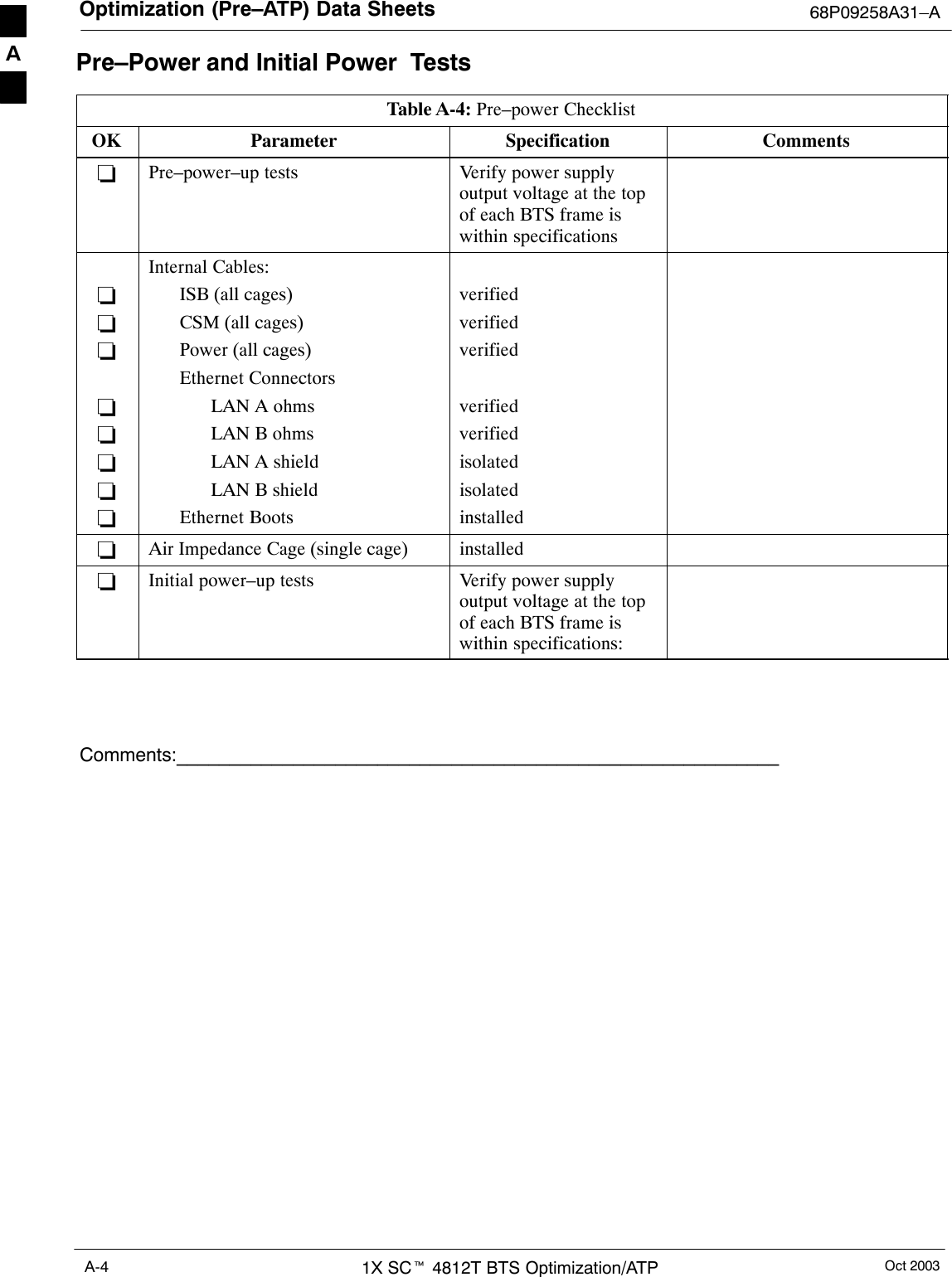
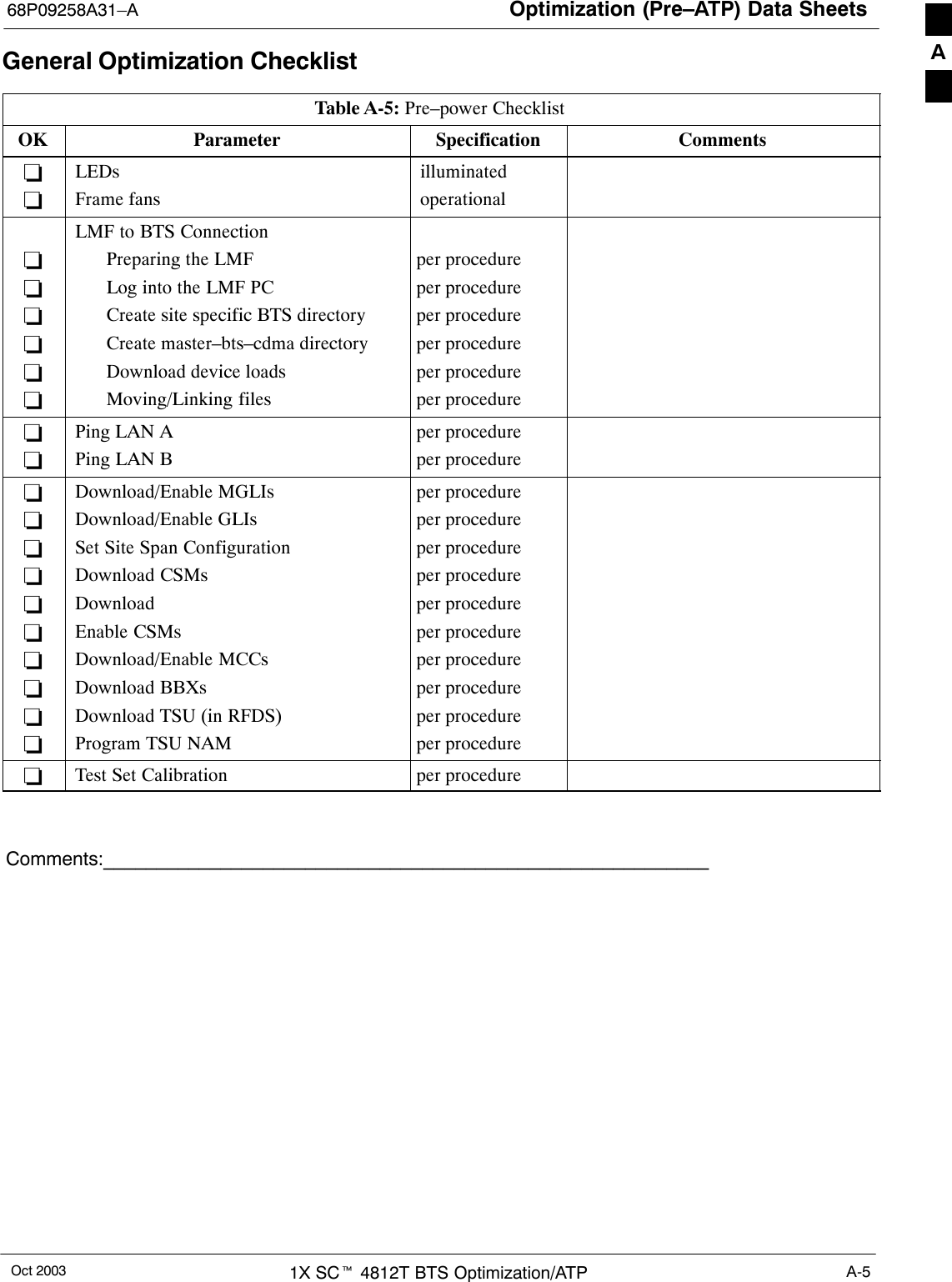
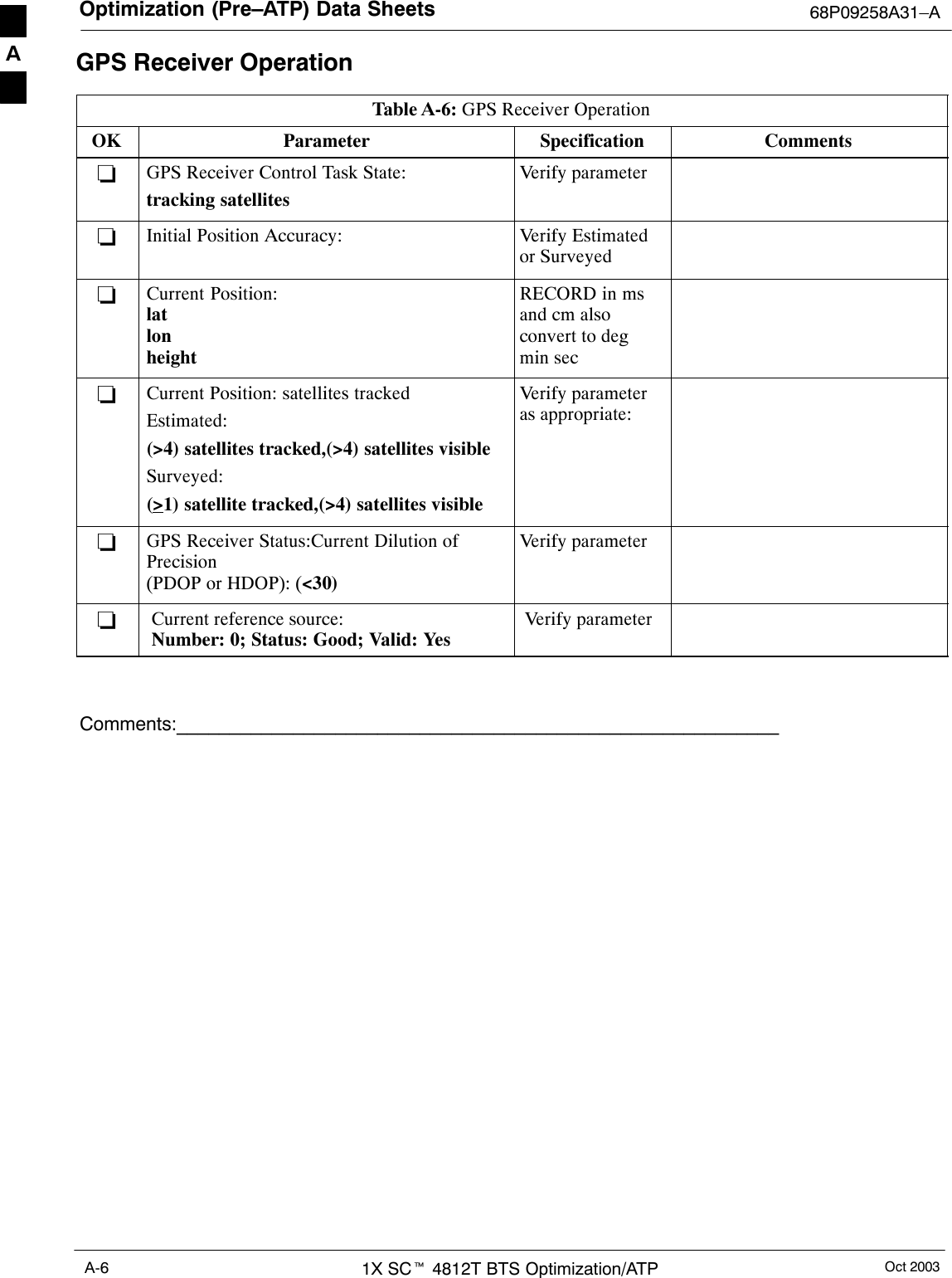
C–CCP Backplane Troubleshooting 68P09258A31–AOct 20031X SCt 4812T BTS Optimization/ATP6-18No (or Missing) MCC Channel ElementsPerform the procedure in Table 6-21 to troubleshoot a channel elementsfailure.Table 6-21: No MCC Channel ElementsStep Action1Verify MCC channel elements (CEs) are correct. MCCTYPE codes are: MCC8E=0, MCC24E=2,MCC–1X=3.2If the problem seems to be limited to one MCC, replace the MCC with a known good MCC.– Check connectors (both board and backplane) for damage.3If no CEs on any MCC:– Verify clock reference to CIO.6
C–CCP Backplane Troubleshooting68P09258A31–AOct 2003 1X SCt 4812T BTS Optimization/ATP 6-19DC Power ProblemsPerform the procedure in Table 6-22 to troubleshoot a DC input voltageto power supply module failure.WARNING Potentially lethal voltage and current levels are routed to theBTS equipment. This test must be carried out with a secondperson present, acting in a safety role. Remove all rings, jewelry,and wrist watches prior to beginning this test.No DC Input Voltage to Power Supply ModuleTable 6-22: No DC Input Voltage to Power Supply ModuleStep Action1Verify DC power is applied to the BTS frame.2Verify there are no breakers tripped.* IMPORTANTIf a breaker has tripped, remove all modules from the applicable shelf supplied by the breaker andattempt to reset it.– If the breaker trips again, there is probably a cable or breaker problem within the frame.– If the breaker does not trip, there is probably a defective module or sub–assembly within the shelf.3Verify that the C–CCP shelf breaker on the BTS frame breaker panel is functional.4Use a voltmeter to determine if the input voltage is being routed to the C–CCP backplane bymeasuring the DC voltage level on the PWR_IN cable.– If the voltage is not present, there is probably a cable or breaker problem within the frame.– If the voltage is present at the connector, reconnect and measure the level at the “VCC” powerfeed clip on the distribution backplane.– If the voltage is correct at the power clip, inspect the clip for damage.5If everything appears to be correct, visually inspect the power supply module connectors.6Replace the power supply module with a known good module.7If steps 1 through 5 fail to indicate a problem, a C–CCP backplane failure (possibly an open trace) hasoccurred.6
C–CCP Backplane Troubleshooting 68P09258A31–AOct 20031X SCt 4812T BTS Optimization/ATP6-20No DC Voltage (+5, +6.5, or +15 Volts) to a Specific GLI,BBX, or SwitchboardPerform the procedure in Table 6-23 to troubleshoot a DC input voltageto GLI, BBX, or Switchboard failure.Table 6-23: No DC Input Voltage to any C–CCP Shelf ModuleStep Action1Verify the steps in Table 6-22 have been performed.2Inspect the defective board/module (both board and backplane) connector for damage.3Replace suspect board/module with known good board/module.TX and RX Signal Routing ProblemsPerform the procedure in Table 6-24 to troubleshoot TX and RX signalrouting problems.Table 6-24: TX and RX Signal Routing ProblemsStep Action1Inspect all Harting Cable connectors and back–plane connectors for damage in all the affected boardslots.2Perform steps in the RF path troubleshooting flowchart in this manual.6
Module Front Panel LED Indicators and Connectors68P09258A31–AOct 2003 1X SCt 4812T BTS Optimization/ATP 6-21Module Front Panel LED Indicators and ConnectorsModule Status IndicatorsEach of the non-passive plug-in modules has a bi-color (green & red)LED status indicator located on the module front panel. The indicator islabeled PWR/ALM. If both colors are turned on, the indicator is yellow.Each plug-in module, except for the fan module, has its own alarm(fault) detection circuitry that controls the state of the PWR/ALM LED.The fan TACH signal of each fan module is monitored by the AMR.Based on the status of this signal, the AMR controls the state of thePWR/ALM LED on the fan module.LED Status Combinations for All Modules (except GLI, CSM, BBX, MCC)PWR/ALM LEDThe following list describes the states of the module status indicator.SSolid GREEN –  module operating in a normal (fault free) condition.SSolid RED – module is operating in a fault (alarm) condition due toelectrical hardware failure.Note that a fault (alarm) indication may or may not be due to a completemodule failure and normal service may or may not be reduced orinterrupted.DC/DC Converter LED Status CombinationsThe PWR CNVTR has alarm (fault) detection circuitry that controls thestate of the PWR/ALM LED. This is true for both the C–CCP and LPApower converters.PWR/ALM LEDThe following list describes the states of the bi-color LED.SSolid GREEN –  module operating in a normal (fault free) condition.SSolid RED –  module is operating in a fault (alarm) condition due toelectrical hardware problem.6
Module Front Panel LED Indicators and Connectors 68P09258A31–AOct 20031X SCt 4812T BTS Optimization/ATP6-22CSM LED Status CombinationsPWR/ALM LEDThe CSMs include on-board alarm detection. Hardware andsoftware/firmware alarms are indicated via the front panel indicators.After the memory tests, the CSM loads OOS–RAM code from the FlashEPROM, if available. If not available, the OOS–ROM code is loadedfrom the Flash EPROM.SSolid GREEN – module is INS_ACT or INS_STBY no alarm.SSolid RED – Initial power up or module is operating in a fault (alarm)condition.SSlowly Flashing GREEN – OOS_ROM no alarm.SLong RED/Short GREEN – OOS_ROM alarm.SRapidly Flashing GREEN – OOS_RAM no alarm or INS_ACT inDUMB mode.SShort RED/Short GREEN – OOS_RAM alarm.SLong GREEN/Short RED – INS_ACT  or INS_STBY alarm.SOff – no DC power  or on-board fuse is open.SSolid YELLOW – After a reset, the CSMs begin to boot. DuringSRAM test and Flash EPROM code check, the LED is yellow. (IfSRAM or Flash EPROM fail, the LED changes to a solid RED andthe CSM attempts to reboot.)Figure 6-1: CSM Front Panel Indicators & Monitor PortsPWR/ALMIndicatorFREQMONITORSYNCMONITORFW00303 . . . continued on next page6
Module Front Panel LED Indicators and Connectors68P09258A31–AOct 2003 1X SCt 4812T BTS Optimization/ATP 6-23FREQ Monitor ConnectorA test port provided at the CSM front panel via a BNC receptacle allowsmonitoring of the 19.6608 MHz clock generated by the CSM. Whenboth CSM 1 and CSM 2 are in an in-service (INS) condition, the CSM 2clock signal frequency is the same as that output by CSM 1.The clock is a sine wave signal with a minimum amplitude of +2 dBm(800 mVpp) into a 50 Ω load connected to this port.SYNC Monitor ConnectorA test port provided at the CSM front panel via a BNC receptacle allowsmonitoring of the “Even Second Tick” reference signal generated by theCSMs.At this port, the reference signal is a TTL active high signal with a pulsewidth of 153 nanoseconds.MMI Connector – Only accessible behind front panel. TheRS–232 MMI port connector is intended to be used primarily inthe development or factory environment, but may be used in thefield for debug/maintenance purposes.GLI2 LED Status CombinationsThe GLI2 module has indicators, controls and connectors as describedbelow and shown in Figure 6-2.The operating states of the 5 LEDs are:ACTIVESolid GREEN – GLI2 is active. This means that the GLI2 has shelfcontrol and is providing control of the digital interfaces.Off – GLI2 is not active (i.e., Standby). The mate GLI2 should beactive.MASTERSSolid GREEN – GLI2 is Master (sometimes referred to as MGLI2).SOff – GLI2 is non-master (i.e., Slave).ALARMSSolid RED – GLI2 is in a fault condition or in reset.SWhile in reset transition,  STATUS LED is OFF while GLI2 isperforming ROM boot (about 12 seconds for normal boot).SWhile in reset transition,  STATUS LED is ON while GLI2 isperforming RAM boot (about 4 seconds for normal boot).SOff – No Alarm.6
Module Front Panel LED Indicators and Connectors 68P09258A31–AOct 20031X SCt 4812T BTS Optimization/ATP6-24STATUSSFlashing GREEN– GLI2 is in service (INS), in a stable operatingcondition.SOn – GLI2 is in OOS RAM state operating downloaded code.SOff – GLI2 is in OOS ROM state operating boot code.SPANSSSolid GREEN – Span line is connected and operating.SSolid RED – Span line is disconnected or a fault condition exists.GLI2 Pushbuttons and ConnectorsRESET Pushbutton – Depressing the RESET pushbuttoncauses a partial reset of the CPU and a reset of all board devices.The GLI2 is placed in the OOS_ROM stateMMI Connector – The RS–232MMI port connector is intendedto be used primarily in the development or factory environmentbut may be used in the field for debug/maintenance purposes.LAN Connectors (A & B) – The two 10BASE2 Ethernet circuitboard mounted BNC connectors are located on the bottom frontedge of the GLI2; one for each LAN interface, A & B. Ethernetcabling is connected to tee connectors fastened to these BNCconnectors.6
Module Front Panel LED Indicators and Connectors68P09258A31–AOct 2003 1X SCt 4812T BTS Optimization/ATP 6-25Figure 6-2: GLI2 Front PanelMMI PORTCONNECTORACTIVE LEDSTATUS RESET ALARM SPANS MASTER MMI ACTIVESTATUS LEDRESETPUSHBUTTONALARM LEDSPANS LEDMASTER LEDSTATUS OFF – operating normallyON – briefly during power-up when the Alarm LED turnsOFF.SLOW GREEN – when the GLI2 is INS (in-service)RESETALARMOFF – operating normallyON – briefly during power-up when the Alarm LED turnsOFF.SLOW GREEN – when the GLI2 is INS (in-service)SPANSMASTERMMI PORTCONNECTORACTIVELED OPERATING STATUSAll functions on the GLI2 are reset when pressing andreleasing the switch.ON – operating normally in active modeOFF – operating normally in standby modeShows the operating status of the redundant cards. Theredundant card toggles automatically if the active card isremoved or failsON – active card operating normallyOFF – standby card operating normallyThe pair of GLI2 cards include a redundant status. Thecard in the top shelf is designated by hardware as theactive card; the card in the bottom shelf is in the standbymode.OFF – card is powered down, in initialization, or in standbyGREEN – operating normallyYELLOW – one or more of the equipped initialized spans isreceiving a remote alarm indication signal from the far endRED – one or more of the equipped initialized spans is in analarm stateAn RS-232, serial, asynchronous communications link foruse as an MMI port. This port supports 300 baud, up to amaximum of 115,200 baud communications.FW002256
Module Front Panel LED Indicators and Connectors 68P09258A31–AOct 20031X SCt 4812T BTS Optimization/ATP6-26GLI3 Front PanelFigure 6-3 shows the GLI3 front panel.Figure 6-3: GLI3 Front PanelSTATUS OFF – operating normallyON – briefly during power-up when the Alarm LED turnsOFFSLOW GREEN – when the GLI3 is INS (in-service)RESETALARMOFF – operating normallyON – briefly during power-up when the Alarm LED turnsOFFSLOW GREEN – when the GLI3 is INS (in-service)BPR  ASpanMMIACTIVELED OPERATING STATUSPressing and releasing the switch resets all functions onthe GLI3.Shows the operating status of the redundant cards. Theredundant card toggles automatically if the active card isremoved or failsON – active card operating normallyOFF – standby card operating normallyConnects to either a BPR or expansion cage and is wired asan ethernet client.An RS-232, serial, asynchronous communications link foruse as an MMI port. This port supports 300 baud, up to amaximum of 115,200 baud communications.BPR  BGLIAUXSupports the cross–coupled ethernet circuits to the mate GLIusing a double crossover cable.Wired as an ethernet client for direct connection to a personalcomputer with a standard ethernet cable. It allows connectionof ethernet “sniffer” when the ethernet switch is properlyconfigured for port monitoring.Connects to either a BPR or expansion cage and is wired asan ethernet client.MMI PortReset SwitchDual 100BASE–Tin a single RJ45to Redundant(Mate) GLI3100BASE–TAuxiliary MonitorPortBPR B AUX RESETSPANALARM MMIACTSTA100BASE–T toBTS Packet Routeror Expansion cageSpan (LED)Alarm (LED)Active (LED)Status (LED)GLIBPR Ati-CDMA-WP-00064-v01-ildoc-ftwOFF – card is powered down, in initialization, or in standbyGREEN – operating normallyYELLOW – one or more of the equipped initialized spans isreceiving a remote alarm indication signal from the far endRED – one or more of the equipped initialized spans is in analarm state6
Module Front Panel LED Indicators and Connectors68P09258A31–AOct 2003 1X SCt 4812T BTS Optimization/ATP 6-27BBX LED Status CombinationsPWR/ALM LEDThe BBX module has its own alarm (fault) detection circuitry thatcontrols the state of the PWR/ALM LED.The following list describes the states of the bi-color LED:SSolid GREEN – INS_ACT no alarmSSolid RED Red – initializing or power-up alarmSSlowly Flashing GREEN – OOS_ROM no alarmSLong RED/Short GREEN – OOS_ROM alarmSRapidly Flashing GREEN – OOS_RAM no alarmSShort RED/Short GREEN – OOS_RAM alarmSLong GREEN/Short RED – INS_ACT  alarmMCC LED Status CombinationsThe MCC module has LED indicators and connectors as describedbelow (see Figure 6-4). Note that the figure does not show theconnectors as they are concealed by the removable lens.The LED indicators and their states are as follows:PWR/ALM LEDSRED – fault on moduleACTIVE LEDSOff – module is inactive, off-line, or not processing traffic.SSlowly Flashing GREEN – OOS_ROM no alarm.SRapidly Flashing Green – OOS_RAM no alarm.SSolid GREEN – module is INS_ACT, on-line, processing traffic.PWR/ALM and ACTIVE LEDsSSolid RED – module is powered but is in reset or the BCP is inactive.MMI ConnectorsSThe RS–232 MMI port connector (four-pin) is intended to be usedprimarily in the development or factory environment but may be usedin the field for debugging purposes.SThe RJ–11 ethernet port connector (eight-pin) is intended to be usedprimarily in the development environment but may be used in the fieldfor high data rate debugging purposes.6
Module Front Panel LED Indicators and Connectors 68P09258A31–AOct 20031X SCt 4812T BTS Optimization/ATP6-28Figure 6-4: MCC Front PanelPWR/ALM LEDLENS(REMOVABLE)ACTIVE LEDPWR/ALM ACTIVEPWR/ALMOFF – operating normallyON – briefly during power-up and duringfailure conditionsACTIVELED OPERATING STATUSRAPIDLY BLINKING – Card iscode-loaded but  not enabledSLOW BLINKING – Card is notcode-loadedON – card is code-loaded and enabled(INS_ACTIVE)COLORGREENREDREDON – fault conditionSLOW FLASHING (alternating with green)– CHI  bus inactive on power-upAn alarm is generated in the event of a failureFW00224LPA Shelf LED Status CombinationsLPA Module LEDEach LPA module contains a bi–color LED just above the MMIconnector on the front panel of the module. Interpret this LED asfollows:SGREEN — LPA module is active and is reporting no alarms (Normalcondition).SFlashing GREEN/RED — LPA module is active but is reporting anlow input power condition. If no BBX is keyed, this is normal anddoes not constitute a failure.6
Basic Troubleshooting – Span Control Link68P09258A31–AOct 2003 1X SCt 4812T BTS Optimization/ATP 6-29Basic Troubleshooting – Span Control LinkSpan Problems (No Control Link)Perform the procedure in Table 6-25 to troubleshoot a control linkfailure.Table 6-25: Troubleshoot Control Link FailurenStep Action1Connect the CDMA LMF computer to the MMI port on the applicable MGLI/GLI as shown inFigure 6-5 or Figure 6-6.2Start an MMI communication session with the applicable MGLI/GLI by using the Windowsdesktop shortcut icon.3Once the connection window opens, press the CDMA LMF computer Enter key until the GLI>prompt is obtained.4At the GLI>  prompt, enter:config ni current  <cr>  (equivalent of span view command)The system will respond with a display similar to the following:The frame format in flash is set to use T1_2.Equalization:  Span A – Default (0–131 feet for T1/J1, 120 Ohm for E1)  Span B – Default (0–131 feet for T1/J1, 120 Ohm for E1)  Span C – Default (0–131 feet for T1/J1, 120 Ohm for E1)  Span D – Default (0–131 feet for T1/J1, 120 Ohm for E1)  Span E – Default (0–131 feet for T1/J1, 120 Ohm for E1)  Span F – Default (0–131 feet for T1/J1, 120 Ohm for E1)Linkspeed: Default (56K for T1 D4 AMI, 64K otherwise)Currently, the link is running at the default rate The actual rate is 0NOTEDefaults for span equalization are 0–131 feet for T1/J1 spans and 120 Ohm for E1.Default linkspeed is 56K for T1 D4 AMI spans and 64K for all other types.There is no need to change from defaults unless the OMC–R/CBSC span configuration requires it.5The span configurations loaded in the GLI must match those in the OMCR/CBSC database for theBTS. If they do not, proceed to Table 6-26.6Repeat steps 1 through 5 for all remaining GLIs.7If the span settings are correct, verify the edlc parameters using the show command.Any alarm conditions indicate that the span is not operating correctly.STry looping back the span line from the DSX panel back to the MM, and verify that the loopedsignal is good.SListen for control tone on the appropriate timeslot from the Base Site and MM.8Exit the GLI MMI session and HyperTerminal connection by selecting File from the connectionwindow menu bar, and then Exit from the drop–down menu.9If no TCHs in groomed MCCs (or in whole C–CCP shelf) can process calls, verify that the ISBcabling is correct and that ISB A and ISB B cables are not swapped.6
Basic Troubleshooting – Span Control Link 68P09258A31–AOct 20031X SCt 4812T BTS Optimization/ATP6-30Figure 6-5: MGLI/GLI Board MMI Connection DetailNULL MODEMBOARD(TRN9666A)8–PIN TO 10–PINRS–232 CABLE(P/N 30–09786R01)RS–232CABLE8–PINCDMA LMFCOMPUTERTo MMI portDB9–TO–DB25ADAPTERCOM1 or COM2ACTIVE LEDSTATUS LEDALARM LEDMASTER LEDMMI PortConnectorSPANS LEDRESETPushbuttonGLIti-CDMA-WP-00079-v01-ildoc-ftw6
Basic Troubleshooting – Span Control Link68P09258A31–AOct 2003 1X SCt 4812T BTS Optimization/ATP 6-31Figure 6-6: GLI3 Board MMI Connection DetailNULL MODEMBOARD(TRN9666A)8–PIN TO 10–PINRS–232 CABLE(P/N 30–09786R01)RS–232CABLE8–PINCDMA LMFCOMPUTERTo MMI portDB9–TO–DB25ADAPTERCOM1 or COM2GLI3MMI PortReset SwitchDual 100BASE–Tin a single RJ45to Redundant(Mate) GLI3100BASE–TAuxiliary MonitorPortBPR B AUX RESETSPANALARM MMIACTSTA100BASE–T toBTS Packet Routeror Expansion cageSpan (LED)Alarm (LED)Active (LED)Status (LED)GLIBPR Ati-CDMA-WP-00064-v01-ildoc-ftwREF6
Basic Troubleshooting – Span Control Link 68P09258A31–AOct 20031X SCt 4812T BTS Optimization/ATP6-32Set BTS Site Span ConfigurationTable 6-26 describes how to set the span parameter configuration.NOTE Perform the following procedure ONLY if span configurationsloaded in the MGLI/GLIs do not match those in theOMCR/CBSC data base, AND ONLY when the exactconfiguration data is available. Loading incorrect spanconfiguration data will render the site inoperable.Table 6-26: Set BTS Span Parameter ConfigurationnStep Action1If not previously done, connect the CDMA LMF computer to the MMI port on the applicableMGLI/GLI as shown in Figure 6-5.2If there is no MMI communication session in progress with the applicable MGLI/GLI, initiate oneby using the Windows desktop shortcut icon.3At the GLI>  prompt, enter:config  ni  format  <option>  <cr> The terminal will display a response similar to the following:COMMAND SYNTAX: config ni format option Next available options:   LIST –  Option : Span Option         E1_1 : E1_1 – E1 HDB3 CRC4    no TS16            E1_2 : E1_2 – E1 HDB3 no CRC4 no TS16            E1_3 : E1_3 – E1 HDB3 CRC4    TS16           E1_4 : E1_4 – E1 HDB3 no CRC4 TS16           T1_1 : T1_1 – D4, AMI, No ZCS          T1_2 : T1_2 – ESF, B8ZS          J1_1 : J1_1 – ESF, B8ZS (Japan) – Default          J1_2 : J1_2 – ESF, B8ZS          T1_3 : T1_3 – D4, AMI, ZCS>NOTEWith this command, all active (in–use) spans will be set to the same format.4To set or change the span type, enter the correct option from the list at the entry prompt (>), asshown in the following example:> T1_2 <cr> NOTEThe entry is case–sensitive and must be typed exactly as it appears in the list. If the entry is typedincorrectly, a response similar to the following will be displayed:CP:  Invalid commandGLI2>5An acknowledgement similar to the following will be displayed:The value has been programmed. It will take effect after the next reset.GLI2>. . . continued on next page6
Basic Troubleshooting – Span Control Link68P09258A31–AOct 2003 1X SCt 4812T BTS Optimization/ATP 6-33Table 6-26: Set BTS Span Parameter ConfigurationnActionStep6If the current MGLI/GLI span rate must be changed, enter the following MMI command:config  ni  linkspeed <cr> The terminal will display a response similar to the following:Next available options: LIST –  linkspeed : Span Linkspeed                   56K : 56K (default for T1_1 and T1_3 systems)                  64K : 64K (default for all other span configurations)>NOTEWith this command, all active (in–use) spans will be set to the same linkspeed.7To set or change the span linkspeed, enter the required option from the list at the entry prompt (>),as shown in the following example:>64K <cr>NOTEThe entry is case–sensitive and must be typed exactly as it appears in the list. If the entry is typedincorrectly, a response similar to the following will be displayed:CP: Invalid commandGLI2>8An acknowledgement similar to the following will be displayed:The value has been programmed.  It will take effect after the next reset.GLI2>9If the span equalization must be changed, enter the following MMI command:config ni equal<cr>The terminal will display a response similar to the following:COMMAND SYNTAX: config ni equal span equalNext available options:   LIST –       span : Span                       a : Span A                       b : Span B                       c : Span C                       d : Span D                       e : Span E                       f : Span F>. . . continued on next page6
Basic Troubleshooting – Span Control Link 68P09258A31–AOct 20031X SCt 4812T BTS Optimization/ATP6-34Table 6-26: Set BTS Span Parameter ConfigurationnActionStep10 At the entry prompt (>), enter the designator from the list for the span to be changed as shown inthe following example:>a<cr> The terminal will display a response similar to the following:COMMAND SYNTAX: config ni equal a equal Next available options:   LIST –      equal :  Span Equalization                        0 : 0–131 feet (default for T1/J1)                        1 : 132–262 feet                        2 : 263–393 feet                        3 : 394–524 feet                        4 : 525–655 feet                        5 : LONG HAUL                         6 : 75 OHM                        7 : 120 OHM (default for E1)>11 At the entry prompt (>), enter the code for the required equalization from the list as shown in thefollowing example:>0<cr> The terminal will display a response similar to the following:> 0The value has been programmed. It will take effect after the next reset.GLI2>12 Repeat Steps 9 through 11 for each in–use span.NOTE– After executing the config  ni  format, config ni linkspeed, and/or config  ni  equalcommands, the affected MGLI/GLI board MUST be reset and reloaded for changes to takeeffect.– Although defaults are shown, always consult site specific documentation for span type andlinkspeed used at the site.13 Press the RESET button on the MGLI/GLI for changes to take effect.14 Once the MGLI/GLI has reset, execute the following command to verify span settings are asrequired:config ni current  <cr>  (equivalent of span view command)The system will respond with a display similar to the following:The frame format in flash is set to use T1_2.Equalization:  Span A – 0–131 feet  Span B – 0–131 feet  Span C – Default (0–131 feet for T1/J1, 120 Ohm for E1)  Span D – Default (0–131 feet for T1/J1, 120 Ohm for E1)  Span E – Default (0–131 feet for T1/J1, 120 Ohm for E1)  Span F – Default (0–131 feet for T1/J1, 120 Ohm for E1)Linkspeed: 64KCurrently, the link is running at 64KThe actual rate is 0. . . continued on next page6
Basic Troubleshooting – Span Control Link68P09258A31–AOct 2003 1X SCt 4812T BTS Optimization/ATP 6-35Table 6-26: Set BTS Span Parameter ConfigurationnActionStep15 If the span configuration is not correct, perform the applicable step from this table to change it andrepeat Steps 13 and 14 to verify required changes have been programmed.16 Return to Step 6 of Table 6-25. 6
Basic Troubleshooting – Span Control Link 68P09258A31–AOct 20031X SCt 4812T BTS Optimization/ATP6-36Notes6
Oct 2003 1X SCt 4812T BTS Optimization/ATP A-1Appendix AData SheetsA
Optimization (Pre–ATP) Data Sheets 68P09258A31–AOct 20031X SCt 4812T BTS Optimization/ATPA-2Optimization (Pre–ATP) Data SheetsVerification of Test Equipment UsedTable A-1: Verification of Test Equipment UsedManufacturer Model Serial NumberComments:__________________________________________________________________________________________________________________________A
Optimization (Pre–ATP) Data Sheets68P09258A31–AOct 2003 1X SCt 4812T BTS Optimization/ATP A-3Site ChecklistTable A-2: Site ChecklistOK Parameter Specification Comments−Deliveries Per established procedures−Floor Plan Verified−−−Inter Frame Cables:EthernetFrame GroundPowerPer procedurePer procedurePer procedure−−−Factory Data:BBXTest PanelRFDSPer procedurePer procedurePer procedure−Site Temperature−Dress Covers/BracketsPreliminary OperationsTable A-3: Preliminary OperationsOK Parameter Specification Comments−Shelf ID Dip Switches Per site equipage−BBX Jumpers Verified per procedure−Ethernet LAN verification Verified per procedureComments:_________________________________________________________A
Optimization (Pre–ATP) Data Sheets 68P09258A31–AOct 20031X SCt 4812T BTS Optimization/ATPA-4Pre–Power and Initial Power  TestsTable A-4: Pre–power ChecklistOK Parameter Specification Comments−Pre–power–up tests Verify power supplyoutput voltage at the topof each BTS frame iswithin specifications−−−−−−−−Internal Cables:ISB (all cages)CSM (all cages)Power (all cages)Ethernet ConnectorsLAN A ohmsLAN B ohmsLAN A shieldLAN B shieldEthernet Bootsverifiedverifiedverifiedverifiedverifiedisolatedisolatedinstalled−Air Impedance Cage (single cage) installed−Initial power–up tests Verify power supplyoutput voltage at the topof each BTS frame iswithin specifications:Comments:_________________________________________________________A
Optimization (Pre–ATP) Data Sheets68P09258A31–AOct 2003 1X SCt 4812T BTS Optimization/ATP A-5General Optimization ChecklistTable A-5: Pre–power ChecklistOK Parameter Specification Comments−−LEDsFrame fansilluminatedoperational−−−−−−LMF to BTS ConnectionPreparing the LMFLog into the LMF PCCreate site specific BTS directoryCreate master–bts–cdma directoryDownload device loadsMoving/Linking filesper procedureper procedureper procedureper procedureper procedureper procedure−−Ping LAN APing LAN Bper procedureper procedure−−−−−−−−−−Download/Enable MGLIsDownload/Enable GLIsSet Site Span ConfigurationDownload CSMsDownloadEnable CSMsDownload/Enable MCCsDownload BBXsDownload TSU (in RFDS)Program TSU NAMper procedureper procedureper procedureper procedureper procedureper procedureper procedureper procedureper procedureper procedure−Test Set Calibration per procedureComments:_________________________________________________________A
Optimization (Pre–ATP) Data Sheets 68P09258A31–AOct 20031X SCt 4812T BTS Optimization/ATPA-6GPS Receiver OperationTable A-6: GPS Receiver OperationOK Parameter Specification Comments−GPS Receiver Control Task State:tracking satellitesVerify parameter−Initial Position Accuracy: Verify Estimatedor Surveyed−Current Position:latlonheightRECORD in msand cm alsoconvert to degmin sec−Current Position: satellites trackedEstimated:(>4) satellites tracked,(>4) satellites visibleSurveyed:(>1) satellite tracked,(>4) satellites visibleVerify parameteras appropriate:−GPS Receiver Status:Current Dilution ofPrecision (PDOP or HDOP): (<30)Verify parameter−Current reference source:Number: 0; Status: Good; Valid: YesVerify parameterComments:_________________________________________________________A
Optimization (Pre–ATP) Data Sheets68P09258A31–AOct 2003 1X SCt 4812T BTS Optimization/ATP A-7LFR Receiver OperationTable A-7: LFR Receiver OperationOK Parameter Specification Comments−Station call letters M X Y Zassignment.as specified in sitedocumentation−SN ratio is > 8 dB−LFR Task State: lfrlocked to station xxxxVerify parameter−Current reference source:Number: 1; Status: Good; Valid: YesVerify parameterComments:_________________________________________________________A
Optimization (Pre–ATP) Data Sheets 68P09258A31–AOct 20031X SCt 4812T BTS Optimization/ATPA-8LPA IM ReductionTable A-8: LPA IM ReductionParameter CommentsOKLPACARRIERSpecificationOKLPA#4:1 & 2:13–Sector2:16–SectorDual BP3–SectorDual BP6–SectorSpecification−1A C1 C1 C1 C1 No Alarms−1B C1 C1 C1 C1 No Alarms−1C C1 C1 C1 C1 No Alarms−1D C1 C1 C1 C1 No Alarms−2A C2 C2 C2 No Alarms−2B C2 C2 C2 No Alarms−2C C2 C2 C2 No Alarms−2D C2 C2 C2 No Alarms−3A C3 C1 C1 No Alarms−3B C3 C1 C1 No Alarms−3C C3 C1 C1 No Alarms−3D C3 C1 C1 No Alarms−4A C4 C2 No Alarms−4B C4 C2 No Alarms−4C C4 C2 No Alarms−4D C4 C2 No AlarmsA
Optimization (Pre–ATP) Data Sheets68P09258A31–AOct 2003 1X SCt 4812T BTS Optimization/ATP A-9LPA ConvergenceTable A-9: LPA ConvergenceOK Parameter Specification DataLPA # Converged−1A Verify per procedure & uploadconvergence data−1B convergence data−1C−1D−2A Verify per procedure & uploadconvergence data−2B convergence data−2C−2D−3A Verify per procedure & uploadconvergence data−3B convergence data−3C−3D−4A Verify per procedure & uploadconvergence data−4B convergence data−4C−4DA
Optimization (Pre–ATP) Data Sheets 68P09258A31–AOct 20031X SCt 4812T BTS Optimization/ATPA-10TX BLO/Power Output Verification for 3–Sector Configurations1–Carrier2–Carrier Non–adjacent Channels4–Carrier Non–adjacent ChannelsTable A-10: TX BLO Calibration (3–S: 1–C, and 2– and 4–C Non–adjacent Channels)OK Parameter Specification Comments−BBX–1, ANT–1 =  dBBBX–r, ANT–1 =  dB−Calibratecarrier 1TX Bay Level Offset = 42 dB (+4 dB)prior to calibrationBBX–2, ANT–2 =  dBBBX–r, ANT–2 =  dB−BBX–3, ANT–3 =  dBBBX–r, ANT–3 =  dB−BBX–7, ANT–1 =  dBBBX–r, ANT–1 =  dB−Calibratecarrier 2TX Bay Level Offset = 42 dB (+4 dB)prior to calibrationBBX–8, ANT–2 =  dBBBX–r, ANT–2 =  dB−BBX–9, ANT–3 =  dBBBX–r, ANT–3 =  dB−BBX–4, ANT–1 =  dBBBX–r, ANT–1 =  dB−Calibratecarrier 3TX Bay Level Offset = 42 dB (+4 dB)prior to calibrationBBX–5, ANT–2 =  dBBBX–r, ANT–2 =  dB−BBX–6, ANT–3 =  dBBBX–r, ANT–3 =  dB−BBX–10, ANT–1 =  dBBBX–r, ANT–1 =  dB−Calibratecarrier 4TX Bay Level Offset = 42 dB (+4 dB)prior to calibrationBBX–11, ANT–2 =  dBBBX–r, ANT–2 =  dB−BBX–12, ANT–3 =  dBBBX–r, ANT–3 =  dB−BBX–1, ANT–1 =  dBBBX–r, ANT–1 =  dB−CalibrationAuditcarrier 10 dB (+0.5 dB) for gain set resolutionpost calibrationBBX–2, ANT–2 =  dBBBX–r, ANT–2 =  dB−carrier 1BBX–3, ANT–3 =  dBBBX–r, ANT–3 =  dB. . . continued on next pageA
Optimization (Pre–ATP) Data Sheets68P09258A31–AOct 2003 1X SCt 4812T BTS Optimization/ATP A-11Table A-10: TX BLO Calibration (3–S: 1–C, and 2– and 4–C Non–adjacent Channels)OK CommentsSpecificationParameter−BBX–7, ANT–1 =  dBBBX–r, ANT–1 =  dB−CalibrationAuditcarrier 20 dB (+0.5 dB) for gain set resolutionpost calibrationBBX–8, ANT–2 =  dBBBX–r, ANT–2 =  dB−carrier 2BBX–9, ANT–3 =  dBBBX–r, ANT–3 =  dB−BBX–4, ANT–1 =  dBBBX–r, ANT–1 =  dB−CalibrationAuditcarrier 30 dB (+0.5 dB) for gain set resolutionpost calibrationBBX–5, ANT–2 =  dBBBX–r, ANT–2 =  dB−carrier 3BBX–6, ANT–3 =  dBBBX–r, ANT–3 =  dB−BBX–10, ANT–1 =  dBBBX–r, ANT–1 =  dB−CalibrationAuditcarrier 40 dB (+0.5 dB) for gain set resolutionpost calibrationBBX–11, ANT–2 =  dBBBX–r, ANT–2 =  dB−carrier 4BBX–12, ANT–3 =  dBBBX–r, ANT–3 =  dB Comments:__________________________________________________________________________________________________________________________2–Carrier Adjacent ChannelTable A-11: TX BLO Calibration (3–S: 2–C Adjacent Channels)OK Parameter Specification Comments−BBX–1, ANT–1 =  dBBBX–r, ANT–1 =  dB−Calibratecarrier 1TX Bay Level Offset = 42 dB (typical),38 dB (minimum) prior to calibrationBBX–2, ANT–2 =  dBBBX–r, ANT–2 =  dB−BBX–3, ANT–3 =  dBBBX–r, ANT–3 =  dB. . . continued on next pageA
Optimization (Pre–ATP) Data Sheets 68P09258A31–AOct 20031X SCt 4812T BTS Optimization/ATPA-12Table A-11: TX BLO Calibration (3–S: 2–C Adjacent Channels)OK CommentsSpecificationParameter−BBX–7, ANT–4 =  dBBBX–r, ANT–4 =  dB−Calibratecarrier 2TX Bay Level Offset = 42 dB (typical),38 dB (minimum) prior to calibrationBBX–8, ANT–5 =  dBBBX–r, ANT–5 =  dB−BBX–9, ANT–6 =  dBBBX–r, ANT–6 =  dB−BBX–1, ANT–1 =  dBBBX–r, ANT–1 =  dB−CalibrationAuditcarrier 10 dB (+0.5 dB) for gain set resolutionpost calibrationBBX–2, ANT–2 =  dBBBX–r, ANT–2 =  dB−carrier 1BBX–3, ANT–3 =  dBBBX–r, ANT–3 =  dB−BBX–7, ANT–4 =  dBBBX–r, ANT–4 =  dB−CalibrationAuditcarrier 20 dB (+0.5 dB) for gain set resolutionpost calibrationBBX–8, ANT–5 =  dBBBX–r, ANT–5 =  dB−carrier 2BBX–9, ANT–6 =  dBBBX–r, ANT–6 =  dB Comments:__________________________________________________________________________________________________________________________3–Carrier Adjacent Channels4–Carrier Adjacent ChannelsTable A-12: TX BLO Calibration (3–S: 3– or 4–C Adjacent Channels)OK Parameter Specification Comments−BBX–1, ANT–1 =  dBBBX–r, ANT–1 =  dB−Calibratecarrier 1TX Bay Level Offset = 42 dB (+4 dB)prior to calibrationBBX–2, ANT–2 =  dBBBX–r, ANT–2 =  dB−BBX–3, ANT–3 =  dBBBX–r, ANT–3 =  dB. . . continued on next pageA
Optimization (Pre–ATP) Data Sheets68P09258A31–AOct 2003 1X SCt 4812T BTS Optimization/ATP A-13Table A-12: TX BLO Calibration (3–S: 3– or 4–C Adjacent Channels)OK CommentsSpecificationParameter−BBX–7, ANT–1 =  dBBBX–r, ANT–1 =  dB−Calibratecarrier 2TX Bay Level Offset = 42 dB (+4 dB)prior to calibrationBBX–8, ANT–2 =  dBBBX–r, ANT–2 =  dB−BBX–9, ANT–3 =  dBBBX–r, ANT–3 =  dB−BBX–4, ANT–4 =  dBBBX–r, ANT–4 =  dB−Calibratecarrier 3TX Bay Level Offset = 42 dB (+4 dB)prior to calibrationBBX–5, ANT–5 =  dBBBX–r, ANT–5 =  dB−BBX–6, ANT–6 =  dBBBX–r, ANT–6 =  dB−BBX–10, ANT–4 =  dBBBX–3, ANT–4 =  dB−Calibratecarrier 4TX Bay Level Offset = 42 dB (+4 dB)prior to calibrationBBX–11, ANT–5 =  dBBBX–r, ANT–5 =  dB−BBX–12, ANT–6 =  dBBBX–r, ANT–6 =  dB−BBX–1, ANT–1 =  dBBBX–r, ANT–1 =  dB−CalibrationAuditcarrier 10 dB (+0.5 dB) for gain set resolutionpost calibrationBBX–2, ANT–2 =  dBBBX–r, ANT–2 =  dB−carrier 1BBX–3, ANT–3 =  dBBBX–r, ANT–3 =  dB−BBX–7, ANT–1 =  dBBBX–r, ANT–1 =  dB−CalibrationAuditcarrier 20 dB (+0.5 dB) for gain set resolutionpost calibrationBBX–8, ANT–2 =  dBBBX–r, ANT–2 =  dB−carrier 2BBX–9, ANT–3 =  dBBBX–r, ANT–3 =  dB. . . continued on next pageA
Optimization (Pre–ATP) Data Sheets 68P09258A31–AOct 20031X SCt 4812T BTS Optimization/ATPA-14Table A-12: TX BLO Calibration (3–S: 3– or 4–C Adjacent Channels)OK CommentsSpecificationParameter−BBX–4, ANT–4 =  dBBBX–r, ANT–4 =  dB−CalibrationAuditcarrier 30 dB (+0.5 dB) for gain set resolutionpost calibrationBBX–5, ANT–5 =  dBBBX–r, ANT–5 =  dB−carrier 3BBX–6, ANT–6 =  dBBBX–r, ANT–6 =  dB−BBX–10, ANT–4 =  dBBBX–r, ANT–4 =  dB−CalibrationAuditcarrier 40 dB (+0.5 dB) for gain set resolutionpost calibrationBBX–11, ANT–5 =  dBBBX–r, ANT–5 =  dB−carrier 4BBX–12, ANT–6 =  dBBBX–r, ANT–6 =  dB Comments:__________________________________________________________________________________________________________________________A
Optimization (Pre–ATP) Data Sheets68P09258A31–AOct 2003 1X SCt 4812T BTS Optimization/ATP A-15TX BLO/Power Output Verification for 6–Sector Configurations1–Carrier2–Carrier Non–adjacent ChannelsTable A-13: TX BLO Calibration (6–S: 1–C, 2–C Non–adjacent Channels)OK Parameter Specification Comments−BBX–1, ANT–1 =  dBBBX–r, ANT–1 =  dB−BBX–2, ANT–2 =  dBBBX–r, ANT–2 =  dB−Calibrate TX Bay Level Offset = 42 dB (typical),BBX–3, ANT–3 =  dBBBX–r, ANT–3 =  dB−carrier 1y ( yp ),38 dB (minimum) prior to calibration BBX–4, ANT–4 =  dBBBX–r, ANT–4 =  dB−BBX–5, ANT–5 =  dBBBX–r, ANT–5 =  dB−BBX–6, ANT–6 =  dBBBX–r, ANT–6 =  dB−BBX–7, ANT–1 =  dBBBX–r, ANT–1 =  dB−BBX–8, ANT–2 =  dBBBX–r, ANT–2 =  dB−Calibrate TX Bay Level Offset = 42 dB (typical),BBX–9, ANT–3 =  dBBBX–r, ANT–3 =  dB−carrier 2y ( yp ),38 dB (minimum) prior to calibration BBX–10, ANT–4 =  dBBBX–3, ANT–4 =  dB−BBX–11, ANT–5 =  dBBBX–r, ANT–5 =  dB−BBX–12, ANT–6 =  dBBBX–r, ANT–5 =  dB. . . continued on next pageA
Optimization (Pre–ATP) Data Sheets 68P09258A31–AOct 20031X SCt 4812T BTS Optimization/ATPA-16Table A-13: TX BLO Calibration (6–S: 1–C, 2–C Non–adjacent Channels)OK CommentsSpecificationParameter−BBX–1, ANT–1 =  dBBBX–r, ANT–1 =  dB−BBX–2, ANT–2 =  dBBBX–r, ANT–2 =  dB−CalibrationAudit0 dB (+0.5 dB) for gain set resolutionBBX–3, ANT–3 =  dBBBX–r, ANT–3 =  dB−Auditcarrier 1()gpost calibration BBX–4, ANT–4 =  dBBBX–r, ANT–4 =  dB−BBX–5, ANT–5 =  dBBBX–r, ANT–5 =  dB−BBX–6, ANT–6 =  dBBBX–r, ANT–6 =  dB−BBX–7, ANT–1 =  dBBBX–r, ANT–1 =  dB−BBX–8, ANT–2 =  dBBBX–r, ANT–2 =  dB−CalibrationAudit0 dB (+0.5 dB) for gain set resolutionBBX–9, ANT–3 =  dBBBX–r, ANT–3 =  dB−Auditcarrier 2()gpost calibration BBX–10, ANT–4 =  dBBBX–r, ANT–4 =  dB−BBX–11, ANT–5 =  dBBBX–r, ANT–5 =  dB−BBX–12, ANT–6 =  dBBBX–r, ANT–6 =  dB Comments:__________________________________________________________________________________________________________________________A
Optimization (Pre–ATP) Data Sheets68P09258A31–AOct 2003 1X SCt 4812T BTS Optimization/ATP A-17BTS Redundancy/Alarm TestsTable A-14: BTS Redundancy/Alarm TestsOK Parameter Specification Data−SIF: Misc. alarm tests Verify per procedure−MGLI redundancy test Verify per procedure−GLI redundancy test Verify per procedure−Power supply/converterredundancyVerify per procedure−Misc. alarm tests Verify per procedure−CSM, GPS, & LFRredundancy/alarm testsVerify per procedure−LPA redundancy test Verify per procedureComments:__________________________________________________________________________________________________________________________TX Antenna VSWRTable A-15: TX Antenna VSWROK Parameter Specification Data−VSWR – Antenna 1   < (1.5 : 1)−VSWR –Antenna 2   < (1.5 : 1)−VSWR –Antenna 3   < (1.5 : 1)−VSWR –Antenna 4   < (1.5 : 1)−VSWR –Antenna 5   < (1.5 : 1)−VSWR –Antenna 6   < (1.5 : 1)Comments:__________________________________________________________________________________________________________________________A
Optimization (Pre–ATP) Data Sheets 68P09258A31–AOct 20031X SCt 4812T BTS Optimization/ATPA-18RX Antenna VSWRTable A-16: RX Antenna VSWROK Parameter Specification Data−VSWR – Antenna 1   < (1.5 : 1)−VSWR –Antenna 2   < (1.5 : 1)−VSWR –Antenna 3   < (1.5 : 1)−VSWR –Antenna 4   < (1.5 : 1)−VSWR –Antenna 5   < (1.5 : 1)−VSWR –Antenna 6   < (1.5 : 1)Comments:_________________________________________________________AMR VerificationTable A-17: AMR CDI Alarm Input VerificationOK Parameter Specification Data−Verify CDI alarm inputoperation (“ALARM A”(numbers 1 –18)BTS Relay #XX –Contact AlarmSets/Clears−Verify CDI alarm inputoperation (“ALARM B” (numbers 19 –36)BTS Relay #XX –Contact AlarmSets/ClearsComments:_________________________________________________________A
Site Serial Number Check List68P09258A31–AOct 2003 1X SCt 4812T BTS Optimization/ATP A-19Site Serial Number Check ListC–CCP ShelfSite I/O A & BC–CCP ShelfCSM–1CSM–2HSOCCD–1CCD–2AMR–1AMR–2MPC–1MPC–2Fans 1–3 GLI–1GLI–2BBX–1BBX–2BBX–3BBX–4BBX–5BBX–6BBX–7BBX–8BBX–9BBX–10BBX–11BBX–12BBX–rMCC–1MCC–2MCC–3MCC–4MCC–5MCC–6MCC–7MCC–8MCC–9A
Site Serial Number Check List 68P09258A31–AOct 20031X SCt 4812T BTS Optimization/ATPA-20MCC–10MCC–11MCC–12CIOSWITCHPS–1PS–2PS–3LPAsLPA 1ALPA 1BLPA 1CLPA 1DLPA 2ALPA 2BLPA 2CLPA 2DLPA 3ALPA 3BLPA 3CLPA 3DLPA 4ALPA 4BLPA 4CLPA 4DPower Conversion Shelf (–48 V BTS Only)AMRPS 4PS 5PS 6PS 7PS 8PS 9A
Oct 2003 1X SCt 4812T BTS Optimization/ATP B-1Appendix BPN Offset/I & Q Offset RegisterProgramming InformationB
PN Offset Programming Information 68P09258A31–AOct 20031X SCt 4812T BTS Optimization/ATPB-2PN Offset Programming InformationPN Offset BackgroundAll channel elements transmitted from a BTS in a particular 1.25 MHzCDMA channel are orthonogonally spread by 1 of 128 possible Walshcode functions; additionally, they are also spread by a quadrature pair ofPN sequences unique to each sector.Overall, the mobile uses this to differentiate multiple signals transmittedfrom the same BTS (and surrounding BTS) sectors, and to synchronizeto the next strongest sector.The PN offset per sector is stored on the BBXs, where the correspondingI & Q registers reside.The PN offset values are determined on a per BTS/per sector(antenna)basis as determined by the appropriate cdf file content. A breakdown ofthis information is found in Table B-1.PN Offset UsageOnly the 14–chip delay is currently in use. It is important to determinethe RF chip delay to be able to test the BTS functionality. This can bedone by ascertaining if the CDF file FineTxAdj  value was set to “on”when the MCC was downloaded with “image data”. The FineTxAdjvalue is used to compensate for the processing delay (approximately20 mS) in the BTS using any type of mobile meeting IS–97specifications.If the FineTxAdj value in the cdf file is 213 (D5 HEX), FineTxAdj hasbeen set for the 14 chip table.NOTE CDF file I and Q values can be represented in DECIMAL orHEX. If using HEX, add 0x before the HEX value. If necessary,convert HEX values in Table B-1 to decimal before comparingthem to cdf file I & Q value assignments.B
PN Offset Programming Information68P09258A31–AOct 2003 1X SCt 4812T BTS Optimization/ATP B-3Table B-1: PnMask I and PnMask Q Values for PilotPn14–Chip  Delay Pilot I Q I Q  PN (Dec.)          (Hex.)0 17523 23459 4473 5BA31 32292 32589 7E24 7F4D2 4700 17398 125C 43F63 14406 26333 3846 66DD4 14899 4011 3A33 0FAB5 17025 2256 4281 08D06 14745 18651 3999 48DB7 2783 1094 0ADF 04468 5832 21202 16C8 52D29 12407 13841 3077 361110 31295 31767 7A3F 7C1711 7581 18890 1D9D 49CA12 18523 30999 485B 791713 29920 22420 74E0 579414 25184 20168 6260 4EC815 26282 12354 66AA 304216 30623 11187 779F 2BB317 15540 11834 3CB4 2E3A18 23026 10395 59F2 289B19 20019 28035 4E33 6D8320 4050 27399 0FD2 6B0721 1557 22087 0615 564722 30262 2077 7636 081D23 18000 13758 4650 35BE24 20056 11778 4E58 2E0225 12143 3543 2F6F 0DD726 17437 7184 441D 1C1027 17438 2362 441E 093A28 5102 25840 13EE 64F029 9302 12177 2456 2F9130 17154 10402 4302 28A231 5198 1917 144E 077D32 4606 17708 11FE 452C33 24804 10630 60E4 298634 17180 6812 431C 1A9C35 10507 14350 290B 380E36 10157 10999 27AD 2AF737 23850 25003 5D2A 61AB38 31425 2652 7AC1 0A5C39 4075 19898 0FEB 4DBA40 10030 2010 272E 07DA41 16984 25936 4258 655042 14225 28531 3791 6F7343 26519 11952 6797 2EB044 27775 31947 6C7F 7CCB45 30100 25589 7594 63F546 7922 11345 1EF2 2C5147 14199 28198 3777 6E2648 17637 13947 44E5 367B49 23081 8462 5A29 210E50 5099 9595 13EB 257B. . . continued on next pageB
PN Offset Programming Information 68P09258A31–AOct 20031X SCt 4812T BTS Optimization/ATPB-4Table B-1: PnMask I and PnMask Q Values for PilotPn14–Chip  Delay Pilot I Q I Q  PN (Dec.)          (Hex.)51 32743 4670 7FE7 123E52 7114 14672 1BCA 395053 7699 29415 1E13 72E754 19339 20610 4B8B 508255 28212 6479 6E34 194F56 29587 10957 7393 2ACD57 19715 18426 4D03 47FA58 14901 22726 3A35 58C659 20160 5247 4EC0 147F60 22249 29953 56E9 750161 26582 5796 67D6 16A462 7153 16829 1BF1 41BD63 15127 4528 3B17 11B064 15274 5415 3BAA 152765 23149 10294 5A6D 283666 16340 17046 3FD4 429667 27052 7846 69AC 1EA668 13519 10762 34CF 2A0A69 10620 13814 297C 35F670 15978 16854 3E6A 41D671 27966 795 6D3E 031B72 12479 9774 30BF 262E73 1536 24291 0600 5EE374 3199 3172 0C7F 0C6475 4549 2229 11C5 08B576 17888 21283 45E0 532377 13117 16905 333D 420978 7506 7062 1D52 1B9679 27626 7532 6BEA 1D6C80 31109 25575 7985 63E781 29755 14244 743B 37A482 26711 28053 6857 6D9583 20397 30408 4FAD 76C884 18608 5094 48B0 13E685 7391 16222 1CDF 3F5E86 23168 7159 5A80 1BF787 23466 174 5BAA 00AE88 15932 25530 3E3C 63BA89 25798 2320 64C6 091090 28134 23113 6DE6 5A4991 28024 23985 6D78 5DB192 6335 2604 18BF 0A2C93 21508 1826 5404 072294 26338 30853 66E2 788595 17186 15699 4322 3D5396 22462 2589 57BE 0A1D97 3908 25000 0F44 61A898 25390 18163 632E 46F399 27891 12555 6CF3 310B100 9620 8670 2594 21DE. . . continued on next pageB
PN Offset Programming Information68P09258A31–AOct 2003 1X SCt 4812T BTS Optimization/ATP B-5Table B-1: PnMask I and PnMask Q Values for PilotPn14–Chip  Delay Pilot I Q I Q  PN (Dec.)          (Hex.)101 6491 1290 195B 050A102 16876 4407 41EC 1137103 17034 1163 428A 048B104 32405 12215 7E95 2FB7105 27417 7253 6B19 1C55106 8382 8978 20BE 2312107 5624 25547 15F8 63CB108 1424 3130 0590 0C3A109 13034 31406 32EA 7AAE110 15682 6222 3D42 184E111 27101 20340 69DD 4F74112 8521 25094 2149 6206113 30232 23380 7618 5B54114 6429 10926 191D 2AAE115 27116 22821 69EC 5925116 4238 31634 108E 7B92117 5128 4403 1408 1133118 14846 689 39FE 02B1119 13024 27045 32E0 69A5120 10625 27557 2981 6BA5121 31724 16307 7BEC 3FB3122 13811 22338 35F3 5742123 24915 27550 6153 6B9E124 1213 22096 04BD 5650125 2290 23136 08F2 5A60126 31551 12199 7B3F 2FA7127 12088 1213 2F38 04BD128 7722 936 1E2A 03A8129 27312 6272 6AB0 1880130 23130 32446 5A5A 7EBE131 594 13555 0252 34F3132 25804 8789 64CC 2255133 31013 24821 7925 60F5134 32585 21068 7F49 524C135 3077 31891 0C05 7C93136 17231 5321 434F 14C9137 31554 551 7B42 0227138 8764 12115 223C 2F53139 15375 4902 3C0F 1326140 13428 1991 3474 07C7141 17658 14404 44FA 3844142 13475 17982 34A3 463E143 22095 19566 564F 4C6E144 24805 2970 60E5 0B9A145 4307 23055 10D3 5A0F146 23292 15158 5AFC 3B36147 1377 29094 0561 71A6148 28654 653 6FEE 028D149 6350 19155 18CE 4AD3150 16770 23588 4182 5C24. . . continued on next pageB
PN Offset Programming Information 68P09258A31–AOct 20031X SCt 4812T BTS Optimization/ATPB-6Table B-1: PnMask I and PnMask Q Values for PilotPn14–Chip  Delay Pilot I Q I Q  PN (Dec.)          (Hex.)151 14726 10878 3986 2A7E152 25685 31060 6455 7954153 21356 30875 536C 789B154 12149 11496 2F75 2CE8155 28966 24545 7126 5FE1156 22898 9586 5972 2572157 1713 20984 06B1 51F8158 30010 30389 753A 76B5159 2365 7298 093D 1C82160 27179 18934 6A2B 49F6161 29740 23137 742C 5A61162 5665 24597 1621 6015163 23671 23301 5C77 5B05164 1680 7764 0690 1E54165 25861 14518 6505 38B6166 25712 21634 6470 5482167 19245 11546 4B2D 2D1A168 26887 26454 6907 6756169 30897 15938 78B1 3E42170 11496 9050 2CE8 235A171 1278 3103 04FE 0C1F172 31555 758 7B43 02F6173 29171 16528 71F3 4090174 20472 20375 4FF8 4F97175 5816 10208 16B8 27E0176 30270 17698 763E 4522177 22188 8405 56AC 20D5178 6182 28634 1826 6FDA179 32333 1951 7E4D 079F180 14046 20344 36DE 4F78181 15873 26696 3E01 6848182 19843 3355 4D83 0D1B183 29367 11975 72B7 2EC7184 13352 31942 3428 7CC6185 22977 9737 59C1 2609186 31691 9638 7BCB 25A6187 10637 30643 298D 77B3188 25454 13230 636E 33AE189 18610 22185 48B2 56A9190 6368 2055 18E0 0807191 7887 8767 1ECF 223F192 7730 15852 1E32 3DEC193 23476 16125 5BB4 3EFD194 889 6074 0379 17BA195 21141 31245 5295 7A0D196 20520 15880 5028 3E08197 21669 20371 54A5 4F93198 15967 8666 3E5F 21DA199 21639 816 5487 0330200 31120 22309 7990 5725. . . continued on next pageB
PN Offset Programming Information68P09258A31–AOct 2003 1X SCt 4812T BTS Optimization/ATP B-7Table B-1: PnMask I and PnMask Q Values for PilotPn14–Chip  Delay Pilot I Q I Q  PN (Dec.)          (Hex.)201 3698 29563 0E72 737B202 16322 13078 3FC2 3316203 17429 10460 4415 28DC204 21730 17590 54E2 44B6205 17808 20277 4590 4F35206 30068 19988 7574 4E14207 12737 6781 31C1 1A7D208 28241 32501 6E51 7EF5209 20371 6024 4F93 1788210 13829 20520 3605 5028211 13366 31951 3436 7CCF212 25732 26063 6484 65CF213 19864 27203 4D98 6A43214 5187 6614 1443 19D6215 23219 10970 5AB3 2ADA216 28242 5511 6E52 1587217 6243 17119 1863 42DF218 445 16064 01BD 3EC0219 21346 31614 5362 7B7E220 13256 4660 33C8 1234221 18472 13881 4828 3639222 25945 16819 6559 41B3223 31051 6371 794B 18E3224 1093 24673 0445 6061225 5829 6055 16C5 17A7226 31546 10009 7B3A 2719227 29833 5957 7489 1745228 18146 11597 46E2 2D4D229 24813 22155 60ED 568B230 47 15050 002F 3ACA231 3202 16450 0C82 4042232 21571 27899 5443 6CFB233 7469 2016 1D2D 07E0234 25297 17153 62D1 4301235 8175 15849 1FEF 3DE9236 28519 30581 6F67 7775237 4991 3600 137F 0E10238 7907 4097 1EE3 1001239 17728 671 4540 029F240 14415 20774 384F 5126241 30976 24471 7900 5F97242 26376 27341 6708 6ACD243 19063 19388 4A77 4BBC244 19160 25278 4AD8 62BE245 3800 9505 0ED8 2521246 8307 26143 2073 661F247 12918 13359 3276 342F248 19642 2154 4CBA 086A249 24873 13747 6129 35B3250 22071 27646 5637 6BFE. . . continued on next pageB
PN Offset Programming Information 68P09258A31–AOct 20031X SCt 4812T BTS Optimization/ATPB-8Table B-1: PnMask I and PnMask Q Values for PilotPn14–Chip  Delay Pilot I Q I Q  PN (Dec.)          (Hex.)251 13904 1056 3650 0420252 27198 1413 6A3E 0585253 3685 3311 0E65 0CEF254 16820 4951 41B4 1357255 22479 749 57CF 02ED256 6850 6307 1AC2 18A3257 15434 961 3C4A 03C1258 19332 2358 4B84 0936259 8518 28350 2146 6EBE260 14698 31198 396A 79DE261 21476 11467 53E4 2CCB262 30475 8862 770B 229E263 23984 6327 5DB0 18B7264 1912 7443 0778 1D13265 26735 28574 686F 6F9E266 15705 25093 3D59 6205267 3881 6139 0F29 17FB268 20434 22047 4FD2 561F269 16779 32545 418B 7F21270 31413 7112 7AB5 1BC8271 16860 28535 41DC 6F77272 8322 10378 2082 288A273 28530 15065 6F72 3AD9274 26934 5125 6936 1405275 18806 12528 4976 30F0276 20216 23215 4EF8 5AAF277 9245 20959 241D 51DF278 8271 3568 204F 0DF0279 18684 26453 48FC 6755280 8220 29421 201C 72ED281 6837 24555 1AB5 5FEB282 9613 10779 258D 2A1B283 31632 25260 7B90 62AC284 27448 16084 6B38 3ED4285 12417 26028 3081 65AC286 30901 29852 78B5 749C287 9366 14978 2496 3A82288 12225 12182 2FC1 2F96289 21458 25143 53D2 6237290 6466 15838 1942 3DDE291 8999 5336 2327 14D8292 26718 21885 685E 557D293 3230 20561 0C9E 5051294 27961 30097 6D39 7591295 28465 21877 6F31 5575296 6791 23589 1A87 5C25297 17338 26060 43BA 65CC298 11832 9964 2E38 26EC299 11407 25959 2C8F 6567300 15553 3294 3CC1 0CDE. . . continued on next pageB
PN Offset Programming Information68P09258A31–AOct 2003 1X SCt 4812T BTS Optimization/ATP B-9Table B-1: PnMask I and PnMask Q Values for PilotPn14–Chip  Delay Pilot I Q I Q  PN (Dec.)          (Hex.)301 17418 30173 440A 75DD302 14952 15515 3A68 3C9B303 52 5371 0034 14FB304 27254 10242 6A76 2802305 15064 28052 3AD8 6D94306 10942 14714 2ABE 397A307 377 19550 0179 4C5E308 14303 8866 37DF 22A2309 24427 15297 5F6B 3BC1310 26629 10898 6805 2A92311 20011 31315 4E2B 7A53312 16086 19475 3ED6 4C13313 24374 1278 5F36 04FE314 9969 11431 26F1 2CA7315 29364 31392 72B4 7AA0316 25560 4381 63D8 111D317 28281 14898 6E79 3A32318 7327 23959 1C9F 5D97319 32449 16091 7EC1 3EDB320 26334 9037 66DE 234D321 14760 24162 39A8 5E62322 15128 6383 3B18 18EF323 29912 27183 74D8 6A2F324 4244 16872 1094 41E8325 8499 9072 2133 2370326 9362 12966 2492 32A6327 10175 28886 27BF 70D6328 30957 25118 78ED 621E329 12755 20424 31D3 4FC8330 19350 6729 4B96 1A49331 1153 20983 0481 51F7332 29304 12372 7278 3054333 6041 13948 1799 367C334 21668 27547 54A4 6B9B335 28048 8152 6D90 1FD8336 10096 17354 2770 43CA337 23388 17835 5B5C 45AB338 15542 14378 3CB6 382A339 24013 7453 5DCD 1D1D340 2684 26317 0A7C 66CD341 19018 5955 4A4A 1743342 25501 10346 639D 286A343 4489 13200 1189 3390344 31011 30402 7923 76C2345 29448 7311 7308 1C8F346 25461 3082 6375 0C0A347 11846 21398 2E46 5396348 30331 31104 767B 7980349 10588 24272 295C 5ED0350 32154 27123 7D9A 69F3. . . continued on next pageB
PN Offset Programming Information 68P09258A31–AOct 20031X SCt 4812T BTS Optimization/ATPB-10Table B-1: PnMask I and PnMask Q Values for PilotPn14–Chip  Delay Pilot I Q I Q  PN (Dec.)          (Hex.)351 29572 5578 7384 15CA352 13173 25731 3375 6483353 10735 10662 29EF 29A6354 224 11084 00E0 2B4C355 12083 31098 2F33 797A356 22822 16408 5926 4018357 2934 6362 0B76 18DA358 27692 2719 6C2C 0A9F359 10205 14732 27DD 398C360 7011 22744 1B63 58D8361 22098 1476 5652 05C4362 2640 8445 0A50 20FD363 4408 21118 1138 527E364 102 22198 0066 56B6365 27632 22030 6BF0 560E366 19646 10363 4CBE 287B367 26967 25802 6957 64CA368 32008 2496 7D08 09C0369 7873 31288 1EC1 7A38370 655 24248 028F 5EB8371 25274 14327 62BA 37F7372 16210 23154 3F52 5A72373 11631 13394 2D6F 3452374 8535 1806 2157 070E375 19293 17179 4B5D 431B376 12110 10856 2F4E 2A68377 21538 25755 5422 649B378 10579 15674 2953 3D3A379 13032 7083 32E8 1BAB380 14717 29096 397D 71A8381 11666 3038 2D92 0BDE382 25809 16277 64D1 3F95383 5008 25525 1390 63B5384 32418 20465 7EA2 4FF1385 22175 28855 569F 70B7386 11742 32732 2DDE 7FDC387 22546 20373 5812 4F95388 21413 9469 53A5 24FD389 133 26155 0085 662B390 4915 6957 1333 1B2D391 8736 12214 2220 2FB6392 1397 21479 0575 53E7393 18024 31914 4668 7CAA394 15532 32311 3CAC 7E37395 26870 11276 68F6 2C0C396 5904 20626 1710 5092397 24341 423 5F15 01A7398 13041 2679 32F1 0A77399 23478 15537 5BB6 3CB1400 1862 10818 0746 2A42. . . continued on next pageB
PN Offset Programming Information68P09258A31–AOct 2003 1X SCt 4812T BTS Optimization/ATP B-11Table B-1: PnMask I and PnMask Q Values for PilotPn14–Chip  Delay Pilot I Q I Q  PN (Dec.)          (Hex.)401 5850 23074 16DA 5A22402 5552 20250 15B0 4F1A403 12589 14629 312D 3925404 23008 29175 59E0 71F7405 27636 13943 6BF4 3677406 17600 11072 44C0 2B40407 17000 29492 4268 7334408 21913 5719 5599 1657409 30320 7347 7670 1CB3410 28240 12156 6E50 2F7C411 7260 25623 1C5C 6417412 17906 27725 45F2 6C4D413 5882 28870 16FA 70C6414 22080 31478 5640 7AF6415 12183 28530 2F97 6F72416 23082 24834 5A2A 6102417 17435 9075 441B 2373418 18527 32265 485F 7E09419 31902 3175 7C9E 0C67420 18783 17434 495F 441A421 20027 12178 4E3B 2F92422 7982 25613 1F2E 640D423 20587 31692 506B 7BCC424 10004 25384 2714 6328425 13459 18908 3493 49DC426 13383 25816 3447 64D8427 28930 4661 7102 1235428 4860 31115 12FC 798B429 13108 7691 3334 1E0B430 24161 1311 5E61 051F431 20067 16471 4E63 4057432 2667 15771 0A6B 3D9B433 13372 16112 343C 3EF0434 28743 21062 7047 5246435 24489 29690 5FA9 73FA436 249 10141 00F9 279D437 19960 19014 4DF8 4A46438 29682 22141 73F2 567D439 31101 11852 797D 2E4C440 27148 26404 6A0C 6724441 26706 30663 6852 77C7442 5148 32524 141C 7F0C443 4216 28644 1078 6FE4444 5762 10228 1682 27F4445 245 23536 00F5 5BF0446 21882 18045 557A 467D447 3763 25441 0EB3 6361448 206 27066 00CE 69BA449 28798 13740 707E 35AC450 32402 13815 7E92 35F7. . . continued on next pageB
PN Offset Programming Information 68P09258A31–AOct 20031X SCt 4812T BTS Optimization/ATPB-12Table B-1: PnMask I and PnMask Q Values for PilotPn14–Chip  Delay Pilot I Q I Q  PN (Dec.)          (Hex.)451 13463 3684 3497 0E64452 15417 23715 3C39 5CA3453 23101 15314 5A3D 3BD2454 14957 32469 3A6D 7ED5455 23429 9816 5B85 2658456 12990 4444 32BE 115C457 12421 5664 3085 1620458 28875 7358 70CB 1CBE459 4009 27264 0FA9 6A80460 1872 28128 0750 6DE0461 15203 30168 3B63 75D8462 30109 29971 759D 7513463 24001 3409 5DC1 0D51464 4862 16910 12FE 420E465 14091 20739 370B 5103466 6702 10191 1A2E 27CF467 3067 12819 0BFB 3213468 28643 19295 6FE3 4B5F469 21379 10072 5383 2758470 20276 15191 4F34 3B57471 25337 27748 62F9 6C64472 19683 720 4CE3 02D0473 10147 29799 27A3 7467474 16791 27640 4197 6BF8475 17359 263 43CF 0107476 13248 24734 33C0 609E477 22740 16615 58D4 40E7478 13095 20378 3327 4F9A479 10345 25116 2869 621C480 30342 19669 7686 4CD5481 27866 14656 6CDA 3940482 9559 27151 2557 6A0F483 8808 28728 2268 7038484 12744 25092 31C8 6204485 11618 22601 2D62 5849486 27162 2471 6A1A 09A7487 17899 25309 45EB 62DD488 29745 15358 7431 3BFE489 31892 17739 7C94 454B490 23964 12643 5D9C 3163491 23562 32730 5C0A 7FDA492 2964 19122 0B94 4AB2493 18208 16870 4720 41E6494 15028 10787 3AB4 2A23495 21901 18400 558D 47E0496 24566 20295 5FF6 4F47497 18994 1937 4A32 0791498 13608 17963 3528 462B499 27492 7438 6B64 1D0E500 11706 12938 2DBA 328A. . . continued on next pageB
PN Offset Programming Information68P09258A31–AOct 2003 1X SCt 4812T BTS Optimization/ATP B-13Table B-1: PnMask I and PnMask Q Values for PilotPn14–Chip  Delay Pilot I Q I Q  PN (Dec.)          (Hex.)501 14301 19272 37DD 4B48502 23380 29989 5B54 7525503 11338 8526 2C4A 214E504 2995 18139 0BB3 46DB505 23390 3247 5B5E 0CAF506 14473 28919 3889 70F7507 6530 7292 1982 1C7C508 20452 20740 4FE4 5104509 12226 27994 2FC2 6D5A510 1058 2224 0422 08B0511 12026 6827 2EFA 1AAB B
PN Offset Programming Information 68P09258A31–AOct 20031X SCt 4812T BTS Optimization/ATPB-14NotesB
Oct 2003 1X SCt 4812T BTS Optimization/ATP C-1Appendix CFRU Optimization/ATP Test MatrixC
FRU Optimization/ATP Test Matrix 68P09258A31–AOct 20031X SCt 4812T BTS Optimization/ATPC-2FRU Optimization/ATP Test MatrixUsage & BackgroundPeriodic maintenance of a site may also may mandate re–optimization ofspecific portions of the site. An outline of some basic guidelines isincluded in the following tables.NOTE Re–optimization steps listed for any assembly detailed in thetables below must be performed anytime an RF cable associatedwith it is replaced.BTS FrameTable C-1: When RF Optimization is required on the BTSItem Replaced Optimize:C–CCP Shelf All sector TX and RX paths to allCombined CDMA Channel Processor(C–CCP) shelves.Multicoupler/Preselector CardThe three or six affected sector RX paths forthe C–CCP shelf in the BTS frames.BBX board RX and TX paths of the affected C–CCPshelf / BBX board.CIO Card All RX and TX paths of the affectedCDMA carrier.Any LPA Module The affected sector TX path.LPA Backplane The affected sector TX path.LPA Filter The affected sector TX path.Ancillary Frame Item Replaced Optimize:Directional Coupler All affected sector RX and TX paths to allBTS frame shelves.Site filter All affected RX sector paths in all shelvesin all BTS frames.Any RFDS componentor TSU.The RFDS calibration RX & TX paths(MONFWD/GENFWD).C
FRU Optimization/ATP Test Matrix68P09258A31–AOct 2003 1X SCt 4812T BTS Optimization/ATP C-3Inter-frame CablingOptimization must be performed after the replacement of any RF cablingbetween BTS frames.Table C-2: When to Optimize Inter–frame CablingItem Replaced Optimize:Ancillary frame to BTSframe (RX) cablesThe affected sector/antenna RXpaths.BTS frame to ancillary frame(TX) cablesThe affected sector/antenna TX paths.Detailed Optimization/ATP Test MatrixTable C-3 outlines in more detail the tests that would need to beperformed if one of the BTS components were to fail and be replaced. Itis also assumes that all modules are placed OOS–ROM via the LMFuntil full redundancy of all applicable modules is implemented.The following guidelines should also be noted when using this table.NOTE Not every procedure required to bring the site back on line isindicated in Table C-3. It is meant to be used as a guidelineONLY. The table assumes that the user is familiar enough withthe BTS Optimization/ATP procedure to understand which testequipment set ups, calibrations, and BTS site preparation will berequired before performing the Table # procedures referenced.Various passive BTS components (such as the TX and RX directionalcouplers, Preselector IO, CIO; etc.) only call for a TX or RX calibrationaudit to be performed in lieu of a full path calibration. If the RX or TXpath calibration audit fails, the entire RF path calibration will need to berepeated. If the RF path calibration fails, further troubleshooting iswarranted.Whenever any C–CCP BACKPLANE is replaced, it is assumed thatonly power to the C–CCP shelf being replaced is turned off via thebreaker supplying that shelf.Whenever any DISTRIBUTION BACKPLANE is replaced it is assumedthat the power to the entire RFM frame is removed and the PreselectorI/O is replaced. The modem frame should be brought up as if it were anew installation.NOTE If any significant change in signal level results from anycomponent being replaced in the RX or TX signal flow paths, itwould be identified by re–running the RX and TX calibrationaudit command.When the CIO is replaced, the C–CCP shelf remains powered up. TheBBX boards may need to be removed, then re–installed into theiroriginal slots, and re–downloaded (code and BLO data). RX and TXcalibration audits should then be performed.C
FRU Optimization/ATP Test Matrix 68P09258A31–AOct 20031X SCt 4812T BTS Optimization/ATPC-4Table C-3: SC 4812T BTS Optimization and ATP Test MatrixDocTbl#page DescriptionDirectional Coupler (RX)Directional Coupler (TX)RX FilterRX CablesTX CablesMPC/EMPCCIOC–CCP BackplaneBBXMCCCSMLFR/HSOGPSGLILPA Trunking BackplaneLPALPA Bandpass FilterPower Supply ModulesSwitch CardRFDSTable 2-1 2-3Initial Boards/Modules Install,Prelimnary Operations, CDFSite Equipage; etc.DDDDDDDDDDDDDDDDD D** D DTable 2-2Table 2-52-62-14DC Power Pre-Test PhysicalInspect D DTable 2-7 2-15 Initial Power-up D D D D** DTable 3-11 3-34 Ping the Processors D D D D D DTable 3-13 3-38 Download/Enable MGLIs D D DTable 3-13 3-38 Download/Enable GLIs D D DTable 3-14 3-39 Download CSMs D D D DTable 3-14 3-39 Download MCCs D D D DTable 3-14 3-39 Download BBXs D D DTable 3-16 3-41 Enable CSMs D DTable 3-17 3-42 Enable MCCs D DTable 3-20 3-49 GPS Initialization /Verification D D DTable 3-21 3-53 LFR Initialization /Verification D DTable 3-22 3-55 HSO Initialization/Verification D DDRequired** Replace power converters one card at a time so that power to the C–CCP or LPA shelf is not lost. If power tothe C–CCP shelf is lost, all cards in the shelf must be downloaded again.C
FRU Optimization/ATP Test Matrix68P09258A31–AOct 2003 1X SCt 4812T BTS Optimization/ATP C-5Table C-3: SC 4812T BTS Optimization and ATP Test MatrixDocTbl#RFDSSwitch CardPower Supply ModulesLPA Bandpass FilterLPALPA Trunking BackplaneGLIGPSLFR/HSOCSMMCCBBXC–CCP BackplaneCIOMPC/EMPCTX CablesRX CablesRX FilterDirectional Coupler (TX)Directional Coupler (RX)DescriptionpageTable 3-37 3-92 TX Path Calibration 4 4 4 1 1 4* 3 3 47Table 3-38 3-94 Download Offsets to BBX 4 4 1 4 *Table 3-39 3-96 TX Path Calibration Audit 44 4 1 1 4 * 3 3 4 7Table 3-48 3-107 RFDS Path CalibrationProcedure (see Note [)6 6 541 1 6* 3 3 46[RFDS Path Calibration should be performed at initial BTS installation AND after replacement of the RFDS FRU. RFDS Path Calibration is NOT required for other FRU replacement but may be used as an additional fault isolation tool.Table 4-1 4-9 Spectral Purity TX Mask ATP 4 4 14**** *Table 4-1 4-9 Waveform Quality (rho) ATP 4 4 * 1 4* *****Table 4-1 4-9 Pilot Time Offset ATP 4 4 * 1 4* *****Table 4-1 4-9 Code Domain Power / NoiseFloor 4 4 148888****Table 4-1 4-9 FER Test 5 5 5 5 2 2 5 8 8 8 8 * 7*Perform if necessary for additional fault isolation, repair assurance, or site certification.1 Perform on all carrier and sector TX paths to the C–CCP cage.2 Perform on all carrier and sector RX paths to the C–CCP cage.3 Perform on all primary and redundant TX paths of the affected carrier.4 Perform on the affected carrier and sector TX paths. (BBXR replacement affects all carrier and sector TXpaths.)5 Perform on the affected carrier and sector RX paths. (BBXR replacement affects all carrier and sector RXpaths.)6 Perform on all RF paths of the affected carrier and sector (RFDS replacement affects all carriers.)7 Perform with redundant BBX for all sectors on all carriers.8 Verify performance by performing on one sector of one carrier only.C
FRU Optimization/ATP Test Matrix 68P09258A31–AOct 20031X SCt 4812T BTS Optimization/ATPC-6NotesC
Oct 2003 1X SCt 4812T BTS Optimization/ATP D-1Appendix DBBX Gain Set Point vs. BTS OutputD
BBX Gain Set Point vs. BTS Output Considerations 68P09258A31–AOct 20031X SCt 4812T BTS Optimization/ATPD-2BBX Gain Set Point vs. BTS Output ConsiderationsUsage & BackgroundTable D-1 outlines the relationship between the total of all code domainchannel element gain settings (digital root sum of the squares) and theBBX Gain Set Point between 33.0 dBm and 44.0 dBm. The resultant RFoutput (as measured at the top of the BTS in dBm) is shown in the table.The table assumes that the BBX Bay Level Offset (BLO) values havebeen calculated.As an illustration, consider a BBX keyed up to produce a CDMA carrierwith only the Pilot channel (no MCCs forward link enabled). Pilot gainis set to 262. In this case, the BBX Gain Set Point is shown to correlateexactly to the actual RF output anywhere in the 33 to 44 dBm outputrange. (This is the level used to calibrate the BTS).Table D-1: BBX Gain Set Point vs. Actual BTS Output (in dBm)dBm’Gainb44 43 42 41 40 39 38 37 36 35 34 33541 – – – – – – – 43.3 42.3 41.3 40.3 39.3533 – – – – – – – 43.2 42.2 41.2 40.2 39.2525 – – – – – – 44 43 42 41 40 39517 – – – – – – 43.9 42.9 41.9 40.9 39.9 38.9509 – – – – – – 43.8 42.8 41.8 40.8 39.8 38.8501 – – – – – – 43.6 42.6 41.6 40.6 39.6 38.6493 – – – – – – 43.5 42.5 41.5 40.5 39.5 38.5485 – – – – – – 43.4 42.4 41.4 40.4 39.4 38.4477 – – – – – – 43.2 42.2 41.2 40.2 39.2 38.2469 – – – – – – 43.1 42.1 41.1 40.1 39.1 38.1461 – – – – – 43.9 42.9 41.9 40.9 39.9 38.9 37.9453 – – – – – 43.8 42.8 41.8 40.8 39.8 38.8 37.8445 – – – – – 43.6 42.6 41.6 40.6 39.6 38.6 37.6437 – – – – – 43.4 42.4 41.4 40.4 39.4 38.4 37.4429 – – – – – 43.3 42.3 41.3 40.3 39.3 38.3 37.3421 – – – – – 43.1 42.1 41.1 40.1 39.1 38.1 37.1413 – – – – 44 43 42 41 40 39 38 37405 – – – – 43.8 42.8 41.8 40.8 39.8 38.8 37.8 36.8397 – – – – 43.6 42.6 41.6 40.6 39.6 38.6 37.6 36.6389 – – – – 43.4 42.4 41.4 40.4 39.4 38.4 37.4 36.4 . . . continued on next pageD
BBX Gain Set Point vs. BTS Output Considerations68P09258A31–AOct 2003 1X SCt 4812T BTS Optimization/ATP D-3Table D-1: BBX Gain Set Point vs. Actual BTS Output (in dBm)dBm’Gainb333435363738394041424344381 – – – – 43.3 42.3 41.3 40.3 39.3 38.3 37.3 36.3374 – – – – 43.1 42.1 41.1 40.1 39.1 38.1 37.1 36.1366 – – – 43.9 42.9 41.9 40.9 39.9 38.9 37.9 36.9 35.9358 – – – 43.7 42.7 41.7 40.7 39.7 38.7 37.7 36.7 35.7350 – – – 43.5 42.5 41.5 40.5 39.5 38.5 37.5 36.5 35.5342 – – – 43.3 42.3 41.3 40.3 39.3 38.3 37.3 36.3 35.3334 – – – 43.1 42.1 41.1 40.1 39.1 38.1 37.1 36.1 35.1326 – – 43.9 42.9 41.9 40.9 39.9 38.9 37.9 36.9 35.9 34.9318 – – 43.7 42.7 41.7 40.7 39.7 38.7 37.7 36.7 35.7 34.7310 – – 43.5 42.5 41.5 40.5 39.5 38.5 37.5 36.5 35.5 34.5302 – – 43.2 42.2 41.2 40.2 39.2 38.2 37.2 36.2 35.2 34.2294 – 44 43 42 41 40 39 38 37 36 35 34286 – 43.8 42.8 41.8 40.8 39.8 38.8 37.8 36.8 35.8 34.8 33.8278 – 43.5 42.5 41.5 40.5 39.5 38.5 37.5 36.5 35.5 34.5 33.5270 – 43.3 42.3 41.3 40.3 39.3 38.3 37.3 36.3 35.3 34.3 33.3262 44 43 42 41 40 39 38 37 36 35 34 33254 43.7 42.7 41.7 40.7 39.7 38.7 37.7 36.7 35.7 34.7 33.7 –246 43.4 42.4 41.4 40.4 39.4 38.4 37.4 36.4 35.4 34.4 33.4 –238 43.2 42.2 41.2 40.2 39.2 38.2 37.2 36.2 35.2 34.2 33.2 –230 42.9 41.9 40.9 39.9 38.9 37.9 36.9 35.9 34.9 33.9 – –222 42.6 41.6 40.6 39.6 38.6 37.6 36.6 35.6 34.6 33.6 – –214 42.2 41.2 40.2 39.2 38.2 37.2 36.2 35.2 34.2 33.2 – –D
BBX Gain Set Point vs. BTS Output Considerations 68P09258A31–AOct 20031X SCt 4812T BTS Optimization/ATPD-4NotesD
Oct 2003 1X SCt 4812T BTS Optimization/ATP E-1Appendix ECDMA Operating FrequencyE
Operating Frequency – North American PCS Bands 68P09258A31–AOct 20031X SCt 4812T BTS Optimization/ATPE-2Operating Frequency – North American PCS BandsIntroductionProgramming of each of the BTS BBX synthesizers is performed by theBTS GLIs via the CHI bus. This programming data determines thetransmit and receive transceiver operating frequencies (channels) foreach BBX.1900 MHz PCS ChannelsFigure E-1 shows the valid channels for the North American PCS1900 MHz frequency spectrum. There are 10 CDMA wireline ornon–wireline band channels used in a CDMA system (unique percustomer operating system).Figure E-1: North American PCS 1900 MHz Frequency Spectrum  FREQ  (MHz)RX              TX2751175CHANNEL1863.759251851.25251871.25425675 1883.751896.251908.751943.751931.251951.251963.751976.251988.75ADBEFC . . . continued on next pageE
Operating Frequency – North American PCS Bands68P09258A31–AOct 2003 1X SCt 4812T BTS Optimization/ATP E-3Calculating 1900 MHz Center FrequenciesTable E-1 shows selected 1900 MHz CDMA candidate operatingchannels, listed in both decimal and hexadecimal, and the correspondingtransmit, and receive frequencies. Center frequencies (in MHz) forchannels not shown in the table may be calculated as follows:STX = 1930 + 0.05 * Channel#Example: Channel 262TX = 1930 + 0.05*262 = 1943.10 MHzSRX = TX – 80Example: Channel 262RX = 1943.10 – 80 = 1863.10 MHzActual frequencies used depend on customer CDMA system frequencyplan.Each CDMA channel requires a 1.77 MHz frequency segment. Theactual CDMA carrier is 1.23 MHz wide, with a 0.27 MHz guard band onboth sides of the carrier.Minimum frequency separation required between any CDMA carrier andthe nearest NAMPS/AMPS carrier is 900 kHz (center-to-center).Table E-1: 1900 MHz TX and RX Frequency vs. ChannelChannel NumberDecimal       HexTransmit Frequency (MHz)Center FrequencyReceive Frequency (MHz)Center Frequency25 0019 1931.25 1851.2550 0032 1932.50 1852.5075 004B 1933.75 1853.75100 0064 1935.00 1855.00125 007D 1936.25 1856.25150 0096 1937.50 1857.50175 00AF 1938.75 1858.75200 00C8 1940.00 1860.00225 00E1 1941.25 1861.25250 00FA 1942.50 1862.50275 0113 1943.75 1863.75300 012C 1945.00 1865.00325 0145 1946.25 1866.25350 015E 1947.50 1867.50375 0177 1948.75 1868.75400 0190 1950.00 1870.00425 01A9 1951.25 1871.25450 01C2 1952.50 1872.50475 01DB 1953.75 1873.75500 01F4 1955.00 1875.00525 020D 1956.25 1876.25550 0226 1957.50 1877.50575 023F 1958.75 1878.75. . . continued on next pageE
Operating Frequency – North American PCS Bands 68P09258A31–AOct 20031X SCt 4812T BTS Optimization/ATPE-4Table E-1: 1900 MHz TX and RX Frequency vs. ChannelChannel NumberDecimal       HexReceive Frequency (MHz)Center FrequencyTransmit Frequency (MHz)Center Frequency600 0258 1960.00 1880.00625 0271 1961.25 1881.25650 028A 1962.50 1882.50675 02A3 1963.75 1883.75700 02BC 1965.00 1885.00725 02D5 1966.25 1886.25750 02EE 1967.50 1887.50775 0307 1968.75 1888.75800 0320 1970.00 1890.00825 0339 1971.25 1891.25850 0352 1972.50 1892.50875 036B 1973.75 1893.75900 0384 1975.00 1895.00925 039D 1976.25 1896.25950 03B6 1977.50 1897.50975 03CF 1978.75 1898.751000 03E8 1980.00 1900.001025 0401 1981.25 1901.251050 041A 1982.50 1902.501075 0433 1983.75 1903.751100 044C 1985.00 1905.001125 0465 1986.25 1906.251150 047E 1987.50 1807.501175 0497 1988.75 1908.75 E
Operating Frequency – North American PCS Bands68P09258A31–AOct 2003 1X SCt 4812T BTS Optimization/ATP E-5800 MHz CDMA ChannelsFigure E-2 shows the valid channels for the North American cellulartelephone frequency spectrum. There are 10 CDMA wireline ornon–wireline band channels used in a CDMA system (unique percustomer operating system).Figure E-2: North American Cellular Telephone System Frequency SpectrumRX  FREQ(MHz)99110231333334666667716717799CHANNELOVERALL NON–WIRELINE (A)  BANDSOVERALL WIRELINE (B)  BANDS824.040825.000825.030834.990835.020844.980845.010846.480846.510848.970869.040870.000870.030879.990880.020889.980890.010891.480891.510893.970TX  FREQ(MHz)1013694689311356644739777CDMA NON–WIRELINE (A)  BANDCDMA WIRELINE (B)  BANDFW00402Calculating 800 MHz Center FrequenciesTable E-2 shows selected 800 MHz CDMA candidate operatingchannels, listed in both decimal and hexadecimal, and the correspondingtransmit, and receive frequencies. Center frequencies (in MHz) forchannels not shown in the table may be calculated as follows:SChannels 1–777TX = 870 + 0.03 * Channel#Example: Channel 262TX = 870 + 0.03*262 = 877.86 MHzSChannels 1013–1023TX = 870 + 0.03 * (Channel# – 1023)Example: Channel 1015TX = 870 +0.03 *(1015 – 1023) = 869.76 MHzSRX = TX – 45 MHzExample: Channel 262RX = 877.86 –45 = 832.86 MHzTable E-2: 800 MHz TX and RX Frequency vs. ChannelChannel NumberDecimal   HexTransmit Frequency (MHz)Center FrequencyReceive Frequency (MHz)Center Frequency1 0001 870.0300 825.030025 0019 870.7500 825.750050 0032 871.5000 826.5000. . . continued on next pageE
Operating Frequency – North American PCS Bands 68P09258A31–AOct 20031X SCt 4812T BTS Optimization/ATPE-6Table E-2: 800 MHz TX and RX Frequency vs. ChannelChannel NumberDecimal   HexReceive Frequency (MHz)Center FrequencyTransmit Frequency (MHz)Center Frequency75 004B 872.2500 827.2500100 0064 873.0000 828.0000125 007D 873.7500 828.7500150 0096 874.5000 829.5000175 00AF 875.2500 830.2500200 00C8 876.0000 831.0000225 00E1 876.7500 831.7500250 00FA 877.5000 832.5000275 0113 878.2500 833.2500300 012C 879.0000 834.0000325 0145 879.7500 834.7500350 015E 880.5000 835.5000375 0177 881.2500 836.2500400 0190 882.0000 837.0000425 01A9 882.7500 837.7500450 01C2 883.5000 838.5000475 01DB 884.2500 839.2500500 01F4 885.0000 840.0000525 020D 885.7500 840.7500550 0226 886.5000 841.5000575 023F 887.2500 842.2500600 0258 888.0000 843.0000625 0271 888.7500 843.7500650 028A 889.5000 844.5000675 02A3 890.2500 845.2500700 02BC 891.0000 846.0000725 02D5 891.7500 846.7500750 02EE 892.5000 847.5000775 0307 893.2500 848.2500NOTEChannel numbers 778 through 1012 are not used.1013 03F5 869.7000 824.70001023 03FF 870.0000 825.0000 E
Operating Frequency – Korean Bands68P09258A31–AOct 2003 1X SCt 4812T BTS Optimization/ATP E-7Operating Frequency – Korean Bands1700 MHz PCS ChannelsFigure E-3 shows the valid channels for the 1700 MHz PCS frequencyspectrum. The CDMA channels are spaced in increments of 25 (25, 50,75, . . . 575) across the CDMA band.Figure E-3: 1700 MHz PCS Frequency Spectrum  FREQ  (MHz)RX              TX575CHANNEL 1751.25251778.751841.251868.75E
Operating Frequency – Korean Bands 68P09258A31–AOct 20031X SCt 4812T BTS Optimization/ATPE-8Calculating 1700 MHz Center FrequenciesCenter frequency for channels may be calculated as follows:Direction Formula ExampleTX 1840 + (0.05 * Channel#) Channel: 1840 + (0.05 + 25) = 1841.25RX 1750 + (0.05 * Channel#) Channel: 1750 + (0.05 + 25) = 1751.25– Actual frequencies used depend on customer CDMA systemfrequency plan.– Each CDMA channel requires a 1.77 MHz frequency segment. Theactual CDMA carrier is 1.23 MHz wide, with a 0.27 MHz guardband on both sides of the carrier– Minimum frequency separation required between any CDMAcarrier and the nearest NAMPS/AMPS carrier is 900 kHz (center tocenter).Table E-3: 1700 MHz TX and RX Frequency vs. Channel (Korean Bands)Channel NumberDecimal       HexTransmit Frequency (MHz)Center FrequencyReceive Frequency (MHz)Center Frequency25 0019 1841.25 1751.2550 0032 1842.50 1752.5075 004B 1843.75 1753.75100 0064 1845.00 1755.00125 007D 1846.25 1756.25150 0096 1847.50 1757.50175 00AF 1848.75 1758.75200 00C8 1850.00 1760.00225 00E1 1851.25 1761.25250 00FA 1852.50 1762.50275 0113 1853.75 1763.75300 012C 1855.00 1765.00325 0145 1856.25 1766.25350 015E 1857.50 1767.50375 0177 1858.75 1768.75400 0190 1860.00 1770.00425 01A9 1861.25 1771.25450 01C2 1862.50 1772.50475 01DB 1863.75 1773.75500 01F4 1865.00 1775.00525 020D 1866.25 1776.25550 0226 1867.50 1777.50575 023F 1868.75 1778.75E
Oct 2003 1X SCt 4812T BTS Optimization/ATP F-1Appendix FTest Equipment PreparationF
Test Equipment Preparation 68P09258A31–AOct 20031X SCt 4812T BTS Optimization/ATPF-2Test Equipment PreparationPurposeThis appendix provides information on pre–testing set–up for thefollowing test equipment items (not required for the Cybertest test set):SAgilent E7495A test equipment setupSAgilent E4406A transmitter test setSAgilent E4432B signal generatorSAdvantest R3267 spectrum analyzerSAdvantest R3562 signal generatorSAgilent 8935 analyzer (formerly HP 8935)SHP 8921 with PCS interface analyzerSAdvantest R3465 analyzerSMotorola CyberTestSHP 437 power meterSGigatronics 8541C power meterSGPIB adapterPre–testing set–up information covered includes verification and settingGPIB addresses, inter–unit cabling, connectivity testing, pre–test controlsettings, and equipment calibration for items which are not calibratedwith the Calibrate Test Equipment function of the LMF.The following procedures cover verification and changing GPIBaddresses for the various items of CDMA test equipment supported bythe LMF.F
Test Equipment Preparation68P09258A31–AOct 2003 1X SCt 4812T BTS Optimization/ATP F-3Agilent R7495A Test Equipment SetupThis test equipment requires a warm-up period of at least 30 minutesbefore BTS testing or calibration begins.Using the Agilent E7495A with the LMFThe Agilent E7495A does not require the use of the 19MHz frequencyreference; if connected, it will be ignored. The Even Sec SYNCconnection is required.The Agilent E7495A signal generator is only calibrated down to –80db.In order to achieve accurate FER testing, be sure the RX setup includesat least 40db of attenuation. This will ensure the signal generator willoutput sufficient power to operate in the calibrated range.Set the IP Address as described in Table F-1.Table F-1: Set IP Address on Agilent E7495A test setnStep Action1Use the System Button > Controls >IPAdmin to set anIP address on the E7495A as 128.0.0.49, and Netmask to255.255.255.128. ConnectionsIt is recommended that you use a hub with BNC and RJ–45 connections.[Suggested models: Netgear model EN104 (4 port) or EN108 (8 port).Do NOT use model numbers ending with “TP”; those have no BNCconnectors.]The LMF will connect to the hub which in turn is connected to the BTSand to the Agilent E7495A.Agilent E7495A to Hub – This is an Ethernet cable, RJ–45 to RJ–45.LMF to Hub – Use one of the following cables to connect the LMF tothe Hub:– Ethernet cable, RJ–45 to RJ–45 (be sure that the LAN card is set foreither AUTO or to use the RJ–45 only).– Coax cable between LAN card and Hub.  (Use a “T” on the hub andconnect a cable between the other end of the “T” and the BTS LANconnection).Hub to BTS – Use BNC “T” connector on the hub. [If your hub doesn’thave BNC ports, use a BNC to UTP adapter.]F
Test Equipment Preparation 68P09258A31–AOct 20031X SCt 4812T BTS Optimization/ATPF-4Detecting Test EquipmentCheck that no other equipment is connected to the LMF. Agilentequipment must be connected to the LAN to detect it. Then perform theprocedures described in Table F-2.Table F-2: Detecting Agilent E7495A Test EquipmentnStep Action1Click the Tools Menu.2 Choose Options.3 Check Agilent E7495A option in non–GPIB Test Equipment and enter its IP number.4 Click Apply and wait a moment.5 Click Dismiss. Power Sensor CalibrationTable F-3 describes the E7495A Power Sensor Calibration.Table F-3: E7495A Power Sensor CalibrationnStep Action1Display the power meter screen.2Zero the power meter. Make sure you are connected as shown in Figure F-1.– Press the Zero softkey.– Press the Continue softkey.3Calibrate the power meter:– Press Ref CF.– Enter the reference cal factor, reading it off the label on the power sensor head.– Press Calibrate.– Connect the power sensor (see Figure F-2).– Press Continue.– Press Cal Factor.– Enter the cal factor from the label on the power sensor  head. Select a cal factor that’s withinthe operating frequency of the base station. F
Test Equipment Preparation68P09258A31–AOct 2003 1X SCt 4812T BTS Optimization/ATP F-5Figure F-1: Agilent E7495A Pre–Power Sensor Calibration connectionUse onlyAgilent suppliedpower adapterGPSGPIOSerial 1Serial 2Power REF50 MHzSensorExt RefInEven SecondSync InAntennaPort 1RF Out / SWRPort 2RF InPOWER SENSORNOT CONNECTEDFigure F-2: Agilent E7495A Power Sensor Calibration connectionUse onlyAgilent suppliedpower adapterGPSGPIOSerial 1Serial 2Power REF50 MHzSensorExt RefInEven SecondSync InAntennaPort 1RF Out / SWRPort 2RF InPOWER SENSORCONNECTEDCable CalibrationFollow the directions in the WinLMF program to calibrate cables.– Calibrate the short cable (see Figure 3-15 on page 3-64) and two 10dB pads to get a base line and then calibrate the TX and RX setup.Since you need at least 40 dB of loss when doing the FER test, thesetup for RX is the same as TX.ATP SetupTX Path Calibration setup is shown in Test Equipment Setup (seeFigure 3-18 on page 3-67).F
Verifying and Setting GPIB Address 68P09258A31–AOct 20031X SCt 4812T BTS Optimization/ATPF-6Verifying and Setting GPIB AddressAgilent E4406A Transmitter Tester GPIB AddressRefer to Figure F-3 and follow the procedure in Table F-4 to verify and,if necessary, change the Agilent E4406A GPIB address.Figure F-3: Setting Agilent E4406A GPIB AddressSystem KeyBk Sp KeyEnter KeyData Entry KeypadSoftkey ButtonsSoftkey Label Display AreaActive Function Areati-CDMA-WP-00085-v01-ildoc-ftwTable F-4: Verify and Change Agilent E4406A GPIB AddressStep Action1In the SYSTEM section of the instrument front panel, press the System key.– The softkey labels displayed on the right side of the instrument screen will change.2Press the Config I/O softkey button to the right of the instrument screen.– The softkey labels will change.– The current instrument GPIB address will be displayed below the GPIB Address softkey label.3If the current GPIB address is not set to 18, perform the following to change it:3a Press the GPIB Address softkey button. In the on–screen Active Function Area, GPIB Address willbe displayed followed by the current GPIB address.3b On front panel Data Entry keypad, enter the communications system analyzer GPIB address of 18.– The GPIB Address label will change to Enter.– Characters typed with the keypad will replace the current GPIB address in the Active FunctionArea.NOTETo correct an entry, press Bk Sp key to delete one character at a time.3c Press the Enter softkey button or the keypad Enter key to set the new GPIB address.– The Config I/O softkey labels will reappear.– The new GPIB address will be displayed under the GPIB Address softkey label. F
Verifying and Setting GPIB Address68P09258A31–AOct 2003 1X SCt 4812T BTS Optimization/ATP F-7Agilent E4432B Signal Generator GPIB AddressRefer to Figure F-4 and follow the procedure in Table F-5 to verify and,if necessary, change the Agilent E4432B GPIB address.Figure F-4: Setting Agilent E4432B GPIB AddressNumericKeypadSoftkeyButtonsSoftkey LabelDisplay AreaActive EntryAreaBackspaceKeyUtilityKeyTable F-5: Verify and Change Agilent E4432B GPIB AddressStep Action1In the MENUS section of the instrument front panel, press the Utility key.– The softkey labels displayed on the right side of the instrument screen will change.2Press the GPIB/RS232 softkey button to the right of the instrument screen.– The softkey labels will change.– The current instrument GPIB address will be displayed below the GPIB Address softkey label.3If the current GPIB address is not set to 1, perform the following to change it:3a Press the GPIB Address softkey button.– The GPIB Address label and current GPIB address will change to boldface.– In the on–screen Active Entry Area, Address: will be displayed followed by the current GPIBaddress.3b On the front panel Numeric keypad, enter the signal generator GPIB address of 1.– The GPIB Address label will change to Enter.– Characters typed on the keypad will replace the current GPIB address in the Active Entry display.NOTETo correct an entry, press the backspace key at the lower right of the keypad to delete one character ata time.3c Press the Enter softkey button to set the new GPIB address.– The new GPIB address will be displayed under the GPIB Address softkey label. F
Verifying and Setting GPIB Address 68P09258A31–AOct 20031X SCt 4812T BTS Optimization/ATPF-8Advantest R3267 Spectrum Analyzer GPIB AddressRefer to Figure F-5 and perform the procedure in Table F-6 to verifyand, if necessary, change the Advantest R3267 spectrum analyzer GPIBaddress.Figure F-5: Setting Advantest R3267 GPIB AddressonREMOTELEDLCL KeyCONFIGKeySoftkey LableDisplay AreaSoftkeyButtonsKeypad BSKeyENTRKeyTable F-6: Verify and Change Advantest R3267 GPIB AddressStep Action1If the REMOTE LED is lighted, press the LCL key.– The LED extinguishes.2Press the CONFIG key.–CONFIG softkey labels will appear in the softkey label display area of the instrument display.– The current GPIB address will be displayed below the GPIB Address softkey label.3If the current GPIB address is not set to 18, perform the following to change it:3a Press the GPIB Address softkey. A GPIB Address entry window will open in the instrument displayshowing the current GPIB address.3b Enter 18 on the keypad in the ENTRY section of the instrument front panel.– Characters typed on the keypad will replace the address displayed in the GPIB Address entrywindow.NOTETo correct an entry, press the BS (backspace) key at the lower right of the keypad to delete onecharacter at a time.3c Press the ENTR key to the lower right of the keypad to set the new GPIB address.– The GPIB Address entry window closes.– The new address is displayed in the bottom portion of the GPIB Address softkey label. F
Verifying and Setting GPIB Address68P09258A31–AOct 2003 1X SCt 4812T BTS Optimization/ATP F-9Advantest R3562 Signal Generator GPIB AddressSet the GP–IB ADDRESS switch on the rear of the Advantest R3562signal generator to address 1 as shown in Figure F-6.Figure F-6: Advantest R3562 GPIB Address Switch Setting123 4567 854321GP–IP ADDRESS10GPIB Address set to “1”F
Verifying and Setting GPIB Address 68P09258A31–AOct 20031X SCt 4812T BTS Optimization/ATPF-10Agilent 8935 Series E6380 (formerly HP 8935) Test Set GPIB AddressRefer to Figure F-7 and follow the procedure in Table F-7 to verify and,if necessary, change the Agilent 8935 GPIB address.Figure F-7: Agilent 8935 Test SetFW00885PresetCursor ControlShiftInst ConfigLocalNOTE This procedure assumes that the test equipment is set up andready for testing.Table F-7: Verify and/or Change Agilent 8935 (formerly HP 8935) GPIB AddressStep Action1NOTEThe HP I/O configuration MUST be set to Talk & Listen, or no device on the GPIB will beaccessible. (Consult test equipment OEM documentation for additional information as required.)To verify that the GPIB addresses are set correctly, press Shift and LOCAL on the Agilent 8935.– The current HP–IB address is displayed at the top of the screen.NOTEHP–IB is the same as GPIB.2If the current GPIB address is not set to 18, perform the following to change it:2a – Press Shift and Inst Config.2b – Turn the Cursor Control knob to move the cursor to the HP–IB Adrs field.2c – Press the Cursor Control knob to select the field.2d – Turn the Cursor Control knob as required to change the address to 18.2e – Press the Cursor Control knob to set the address.3 Press Preset to return to normal operation.F
Verifying and Setting GPIB Address68P09258A31–AOct 2003 1X SCt 4812T BTS Optimization/ATP F-11Hewlett Packard HP8921A and HP83236A/B GPIB AddressRefer to Figure F-8 and follow the procedure in Table F-8 to verify and,if necessary, change the HP 8921A HP 83236A GPIB addresses.Figure F-8: HP 8921A and HP 83236A/BPresetCursor ControlShiftLocalNOTE This procedure assumes that the test equipment is set up andready for testing.Table F-8: Verify and/or Change HP 8921A and HP 83236A GPIB AddressesStep Action1To verify that the GPIB addresses are set correctly, press Shift and LOCAL on the HP 8921A.– The current HP–IB address is displayed at the top of the screen.NOTEHP–IB is the same as GPIB.2If the current HP–IB address is not set to 18, perform the following to change it:2a – Turn the Cursor Control knob to move the cursor to More and press the knob to select the field.2b – Turn the Cursor Control knob to move the cursor to I/O Config and press the knob to select thefield.2c – Turn the Cursor Control knob to move the cursor to Adrs and press the knob to select the field.2d – Turn the Cursor Control knob to change the HP–IB address to 18 and press the knob to set theaddress.2e – Press Shift and Preset to return to normal operation.3To set the HP 83236A (or B) PCS Interface GPIB address=19, set the DIP switches as follows:– A1=1, A2=1, A3=0, A4=0, A5=1, HP–IB/Ser = 1F
Verifying and Setting GPIB Address 68P09258A31–AOct 20031X SCt 4812T BTS Optimization/ATPF-12Advantest R3465 Communications Test Set GPIB AddressRefer to Figure F-9 and follow the procedure in Table F-9 to verify and,if necessary, change the GPIB address for the Advantest R3465.Figure F-9: R3465 Communications Test SetBNC“T”REF UNLOCK EVENSEC/SYNC IN CDMATIME BASE INPOWEROFF ONREF FW00337LCL Shift PresetGPIB and othersVernierKnobNOTE This procedure assumes that the test equipment is set up andready for testing.Table F-9: Verify and/or Change Advantest R3465 GPIB AddressStep Action1To verify that the GPIB address is set correctly, perform the following:1a – Press SHIFT then PRESET.1b – Press LCL.1c – Press the GPIB and Others CRT menu key to view the current address.2If the current GPIB address is not set to 18, perform the following to change it:2a – Turn the vernier knob as required to select 18.2b – Press the vernier knob to set the address.3To return to normal operation, press Shift and Preset.F
Verifying and Setting GPIB Address68P09258A31–AOct 2003 1X SCt 4812T BTS Optimization/ATP F-13Motorola CyberTest GPIB AddressFollow the steps in Table F-10 to verify and, if necessary, change theGPIB address on the Motorola CyberTest. Changing the GPIB addressrequires the following items:SMotorola CyberTest communications analyzer.SComputer running Windows 3.1/Windows 95.SMotorola CyberTAME software program “TAME”.SParallel printer port cable (shipped with CyberTest).NOTE This procedure assumes that the test equipment is set up andready for testing.Table F-10:  Verify and/or Change Motorola CyberTest GPIB AddressStep Action1On the LMF desktop, locate the CyberTAME icon. Double click on the icon to run the CyberTAMEapplication.2In the CyberTAME window taskbar, under Special, select IEEE.488.2.3CyberTAME software will query the CyberTest Analyzer for its current GPIB address. It then willopen the IEEE 488.2 dialog box. If the current GPIB address is not 18, perform the followingprocedure to change it:3a – Use the up or down increment arrows or double–click in the field and type the number to set theaddress to 18.3b – Click on the OK button.–– The new address will be written to the CyberTest through the parallel port and saved.4Verify that the address has been set by repeating steps 2 and 3.– The new address should now appear in the IEEE 488.2 dialog box Address field.F
Verifying and Setting GPIB Address 68P09258A31–AOct 20031X SCt 4812T BTS Optimization/ATPF-14HP 437 Power Meter GPIB AddressRefer to Figure F-10 and follow the steps in Table F-11 to verify and, ifnecessary, change the HP 437 GPIB address.Figure F-10: HP 437 Power MeterENTERPRESETSHIFT (BLUE) PUSHBUTTON –ACCESSES FUNCTION ANDDATA ENTRY KEYS IDENTIFIEDWITH LIGHT BLUE TEXT ONTHE FRONT PANEL ABOVETHE BUTTONSFW00308REFNOTE This procedure assumes that the test equipment is set up andready for testing.Table F-11: Verify and/or Change HP 437 Power Meter GPIB AddressStep Action1 Press Shift and PRESET.2Use the y arrow  key to navigate to HP–IB ADRS and press ENTER.The HP–IB address is displayed.NOTEHP–IB is the same as GPIB.3If the current GPIB address is not set to 13, perform the following to change it:– Use the y b arrow keys to change the HP–IB ADRS to 13.– Press ENTER to set the address.4 Press Shift and ENTER to return to a standard configuration. F
Verifying and Setting GPIB Address68P09258A31–AOct 2003 1X SCt 4812T BTS Optimization/ATP F-15Gigatronics 8541C Power Meter GPIB AddressRefer to Figure F-11 and follow the steps in Table F-12 to verify and, ifnecessary, change the Gigatronics 8541C power meter GPIB address.Figure F-11: Gigatronics 8541C Power Meter DetailMENU ENTER ARROWKEYS1REF FW00564NOTE This procedure assumes that the test equipment is set up andready for testing.Table F-12: Verify and/or Change Gigatronics 8541C Power Meter GPIB AddressStep Action1! CAUTIONDo not connect/disconnect the power meter sensor cable with AC power applied to the meter.Disconnection could result in destruction of the sensing element or miscalibration.Press MENU.2Use the b arrow key to select CONFIG MENU and press ENTER.3Use the b arrow key to select GPIB and press ENTER.The current Mode and GPIB Address are displayed.4If the Mode is not set to 8541C, perform the following to change it:Use the a ’  arrow keys as required to select MODE.Use the by arrow keys as required to set MODE to 8541C.5If the GPIB address is not set to 13, perform the following to change it:Use the ’ arrow key to select ADDRESS.Use the by arrow keys as required to set the GPIB address to 13.6 Press ENTER to return to normal operation.F
Verifying and Setting GPIB Address 68P09258A31–AOct 20031X SCt 4812T BTS Optimization/ATPF-16RS232 GPIB Interface AdapterBe sure that the RS–232 GPIB interface adapter DIP switches are set asshown in Figure F-12.Figure F-12: RS232 GPIB Interface AdapterRS232–GPIBINTERFACE BOXS MODEDATA FORMATBAUD RATEGPIB ADRSONDIP SWITCH SETTINGSG MODEF
Test Equipment Set-up68P09258A31–AOct 2003 1X SCt 4812T BTS Optimization/ATP F-17Test Equipment Set-upPurposeThis section covers other test equipment and peripherals not covered inChapter 3. Procedures for the manual testing are covered here, alongwith procedures to calibrate the TX and RX cables using the signalgenerator and spectrum analyzer.Equipment Warm upNOTE Warm-up BTS equipment for a minimum of 60 minutes prior toperforming the BTS optimization procedure. This assures BTSsite stability and contributes to optimization accuracy. (Timespent running initial power-up, hardware/firmware audit, and BTS download counts as warm-up time.)CAUTION If any piece of test equipment (i.e., test cable, RF adapter) hasbeen replaced, re-calibration must be performed. Failure to do socould introduce measurement errors, resulting in incorrectmeasurements and degradation to system performance.NOTE Calibration of the communications test set (or equivalent testequipment) must be performed at the site before calibrating theoverall test set. Calibrate the test equipment  after it has beenallowed to warm-up and stabilize for a minimum of 60 minutes.PrerequisitesPrior to performing any of these procedures, all preparations forpreparing the LMF, updating LMF files, and any other pre-calibrationprocedures, as stated in Chapter 3, must have been completed.F
Test Equipment Set-up 68P09258A31–AOct 20031X SCt 4812T BTS Optimization/ATPF-18HP8921A System Connectivity TestFollow the steps in Table F-13 to verify that the connections between thePCS Interface and the HP8921A are correct, and cables are intact. Thesoftware also performs basic functionality checks of each instrument.NOTE Disconnect other GPIB devices, especially system controllers,from the system before running the connectivity software.Table F-13: System ConnectivityStep ActionNOTE– Perform this procedure after test equipment has been allowed to warm–up and stabilize for aminimum of 60 minutes.1Insert HP 83236A Manual Control/System card into memory card slot.2Press the [PRESET] pushbutton.3Press the Screen Control [TESTS] pushbutton to display the “Tests” Main Menu screen.4Position the cursor at Select Procedure Location and select by pressing the cursor control knob.In the Choices selection box, select Card.5Position the cursor at Select Procedure Filename and select by pressing the cursor control knob.In the Choices selection box, select SYS_CONN.6Position the cursor at RUN TEST and select it.The software will prompt you through the connectivity setup.7When the test is complete, position the cursor on STOP TEST and select it; OR press the [K5]pushbutton.8To return to the main menu, press the [K5] pushbutton.F
Test Equipment Set-up68P09258A31–AOct 2003 1X SCt 4812T BTS Optimization/ATP F-19Manual Cable Calibration using HP8921 with HP PCS Interface (HP83236)NOTEThis calibration method must be executed with great care. Somelosses are measured close to the minimum limit of the powermeter sensor (–30 dBm).PrerequisitesEnsure the following prerequisites have been met before proceeding:STest equipment to be calibrated has been connected correctly for cablecalibration.STest equipment has been selected and calibrated.Refer to Figure F-13 for location of the components on the PCSInterface and Communications Test Set.Test Equipment Set-upPerform the procedure in Table F-14 to calibrate the test equipmentusing the HP8921 Cellular Communications Analyzer equipped with theHP83236 PCS Interface.Table F-14: Manual Cable Calibration Test Equipment Setup (using the HP PCS Interface)Step ActionNOTEVerify that GPIB controller is turned off.1Insert HP 83236A Manual Control System card into memory card slot (see Figure F-13).2Press the Preset pushbutton.3 Under Screen Controls, press the TESTS pushbutton to display the TESTS (Main Menu) screen.4Position the cursor at Select Procedure Location and select it. In the Choices selection box, selectCARD.5Position the cursor at Select Procedure Filename and select it. In the Choices selection box, selectMANUAL.6Position the cursor at RUN TEST and select it. HP must be in Control Mode Select YES.7If using HP 83236A:Set channel number=<chan#>:– Position cursor at ChannelNumber and select it.– Enter the chan# using the numerickeypad; press [Enter] and thescreen will go blank.– When the screen reappears, thechan# will be displayed on thechannel number line.If using HP 83236B:Set channel frequency:– Position cursor at Frequency Band and press Enter.– Select User Defined Frequency.– Go Back to Previous Menu.– Position the cursor to 83236 generator frequency andenter actual RX frequency.– Position the cursor to 83236 analyzer frequency andenter actual TX frequency.8Set RF Generator level:– Position the cursor at RF Generator Level and select it.– Enter –10 using the numeric keypad; press [Enter] and the screen will go blank.– When the screen reappears, the value –10 dBm will be displayed on the RF Generator Level line.. . . continued on next pageF
Test Equipment Set-up 68P09258A31–AOct 20031X SCt 4812T BTS Optimization/ATPF-20Table F-14: Manual Cable Calibration Test Equipment Setup (using the HP PCS Interface)Step Action9Set the user fixed Attenuation Setting to 0 dBm:– Position cursor at Analyzer Attenuation and select it– Position cursor at User Fixed Atten Settings and select it.– Enter 0 (zero) using the numeric keypad and press [Enter].10 Select Back to Previous Menu.11 Record the HP83236 Generator Frequency Level:Record the HP83236B Generator Frequency Level:– Position cursor at Show Frequency and Level Details and select it.– Under HP83236 Frequencies and Levels, record the Generator Level.– Under HP83236B Frequencies and Levels, record the Generator Frequency Level(1850 – 1910 MHz for 1.9 GHz or 1750 – 1780 for 1.7 GHz).– Position cursor at Prev Menu and select it.12 Click on Pause for Manual Measurement.13 Connect the power sensor directly to the RF OUT ONLY port of the PCS Interface.14 On the HP8921A, under To Screen, select CDMA GEN.15 Move the cursor to the Amplitude field and click on the Amplitude value.16 Increase the Amplitude value until the power meter reads 0 dBm ±0.2 dB.NOTEThe Amplitude value can be increased coarsely until 0 dBM is reached; then fine tune the amplitudeby adjusting the Increment Set to 0.1 dBm and targeting in on 0 dBm.17 Disconnect the power sensor from the RF OUT ONLY port of the PCS Interface.NOTEThe Power Meter sensor’s lower limit is –30 dBm. Thus, only components having losses ≤30 dBshould be measured using this method. For further accuracy, always re-zero the power meterbefore connecting the power sensor to the component being calibrated. After connecting thepower sensor to the component, record the calibrated loss immediately.18 Disconnect all components in the test setup and calibrate each one separately by connecting eachcomponent, one-at-a-time, between the RF OUT ONLY PORT and the power sensor (see Figure F-13,Setups A, B, or C). Record the calibrated loss value displayed on the power meter.SExample: (A) Test Cable(s) = –1.4 dB(B) 20 dB Attenuator  = –20.1 dB(B) Directional Coupler = –29.8 dB19 After all components are calibrated, reassemble all components together and calculate the total testsetup loss by adding up all the individual losses:SExample: Total test setup loss = –1.4 –29.8 –20.1 = –51.3 dB.This calculated value will be used in the next series of tests.20 Under Screen Controls press the TESTS button to display the TESTS (Main Menu) screen.21 Select Continue (K2).22 Select RF Generator Level and set to –119 dBm.. . . continued on next pageF
Test Equipment Set-up68P09258A31–AOct 2003 1X SCt 4812T BTS Optimization/ATP F-21Table F-14: Manual Cable Calibration Test Equipment Setup (using the HP PCS Interface)Step Action23 Click on Pause for Manual Measurement.24 Verify the HP8921A Communication Analyzer/83203A CDMA interface setup is as follows (fieldsnot indicated remain at default):SVerify the GPIB (HP–IB) address:– under To Screen, select More– select IO CONFIG– Set HP–IB Adrs to 18– set Mode to Talk&LstnSVerify the HP8921A is displaying frequency (instead of RF channel)– Press the blue [SHIFT] button, then press the Screen Control [DUPLEX] button; this switches tothe CONFIG (CONFIGURE) screen.– Use the cursor control to set RF Display to Freq25 Refer to Table 3-31 for assistance in manually setting the cable loss values into the LMF. F
Test Equipment Set-up 68P09258A31–AOct 20031X SCt 4812T BTS Optimization/ATPF-22Figure F-13: Calibrating Test Setup Components(A)(C)POWERSENSOR(A)POWERSENSOR(C)30 dBDIRECTIONALCOUPLER150 WNON–RADIATINGRF LOADPOWERSENSOR(B)POWERSENSOR(B)MEMORYCARDSLOT20 dB / 20 WATTATTENUATORFW00292F
Test Equipment Set-up68P09258A31–AOct 2003 1X SCt 4812T BTS Optimization/ATP F-23HP PCS Interface Test Equipment Setup for Manual TestingFollow the procedure in Table F-15 to setup the HP PCS Interface Boxfor manual testing.Table F-15: HP PCS Interface Test Equipment Setup for Manual TestingnStep ActionNOTEVerify GPIB controller is turned off.1Insert HP83236B Manual Control/System card into the memory card slot.2 Under Screen Controls, press the [TESTS] push-button to display the TESTS (Main Menu)screen.3Position the cursor at Select Procedure Location and select. In the Choices selection box, selectCARD.4Position the cursor at Select Procedure Filename and select. In the Choices selection box, selectMANUAL.5Position the cursor at RUN TEST and select OR press the K1 push-button.6Set channel number=<chan#>:– Position cursor at Channel Number and select.– Enter the chan# using the numeric keypad and then press [Enter] (the screen will blank).– When the screen reappears, the chan# will be displayed on the channel number line.NOTEIf using a TMPC with Tower Top Amplifier (TTA) skip Step 7.7SSet RF Generator level= –119 dBm + Cal factorExample: –119 dBm + 2 dB = –117 dBmSContinue with Step 9 (skip Step 8).8Set RF Generator level= –116 dBm + Cal factor.Example: –116 dBm + 2 dB = –114 dBm9Set the user fixed Attenuation Setting to 0 dB:– Position cursor at RF Generator Level and select.– Position  cursor at User Fixed Atten Settings and select.– Enter 0 (zero) using the numeric keypad and press [Enter].10 Select Back to Previous Menu.11 Select Quit, then select Yes.F
Test Equipment Set-up 68P09258A31–AOct 20031X SCt 4812T BTS Optimization/ATPF-24Calibrating Test Cable Setup using Advantest R3465NOTE Be sure the GPIB Interface is OFF for this procedure.Perform the procedure in Table F-16 to calibrate the test cable setupusing the Advantest R3465. Advantest R3465 Manual Test setup andcalibration must be performed at both the TX and RX frequencies.Table F-16: Procedure for Calibrating Test Cable Setup Using Advantest R3465Step ActionNOTE– This procedure can only be performed after test equipment has been allowed to warm–up andstabilize for a minimum of 60 minutes.1Press the SHIFT and the PRESET keys located below the display.2Press the ADVANCE key in the MEASUREMENT area of the control panel.3Select the CDMA Sig CRT menu key.4Select the Setup CRT menu key.5Using the vernier knob and the cursor keys set the following parameters:NOTEFields not listed remain at default.Generator Mode: SIGNALLink: FORWARDLevel Unit: dBmCalCorrection: ONLevel Offset: OFF6Select the return CRT menu key.7 Press FREQ key in the ENTRY area.8Set the frequency to the desired value using the keypad entry keys.9Verify that the Mod CRT menu key is highlighting OFF; if not, press the Mod key to toggle it OFF.10 Verify that the Output CRT menu key is highlighting OFF; if not, press the Output key to toggle itOFF.11 Press the LEVEL key in the ENTRY area.12 Set the LEVEL to 0 dBm using the key pad entry keys.13 Zero power meter. Next connect the power sensor directly to the “RF OUT” port on the R3561LCDMA Test Source Unit.14 Press the Output CRT menu key to toggle Output to ON.15 Record the power meter reading  ________________________16 Disconnect the power meter sensor from the R3561L RF OUT jack.. . . continued on next pageF
Test Equipment Set-up68P09258A31–AOct 2003 1X SCt 4812T BTS Optimization/ATP F-25Table F-16: Procedure for Calibrating Test Cable Setup Using Advantest R3465Step ActionNOTEThe Power Meter sensor lower limit is –30 dBm. Thus, only components having losses < 30 dBshould be measured using this method. For best accuracy, always re–zero the power meter beforeconnecting the power sensor to the component being calibrated.  Then, after connecting thepower sensor to the component, record the calibrated loss immediately.17 Disconnect all components in the the test setup and calibrate each one separately.  Connect eachcomponent one–at–a–time between the “RF OUT” port and the power sensor (see Figure F-14,“Setups A, B, and C”). Record the calibrated loss value displayed on the power meter for eachconnection.Example:  (A) 1st Test Cable =  –0.5 dB(B) 2nd Test Cable  =  –1.4 dB(C) 20 dB Attenuator  =  –20.1 dB(D) 30 dB Directional Coupler  =  –29.8 dB18 Press the Output CRT menu key to toggle Output OFF.19 Calculate the total test setup loss by adding up all the individual losses:Example:  Total test setup loss  =  0.5 + 1.4 + 20.1 + 29.8  =  51.8 dBThis calculated value will be used in the next series of tests.20 Press the FREQ key in the ENTRY area.21 Using the keypad entry keys, set the test frequency to the RX frequency.22 Repeat steps 9 through 19 for the RX frequency.23 Refer to Table 3-31 for assistance in manually setting the cable loss values into the LMF. F
Test Equipment Set-up 68P09258A31–AOct 20031X SCt 4812T BTS Optimization/ATPF-26Figure F-14: Cable Calibration using Advantest R3465POWERSENSOR20 DB / 2 WATTATTENUATOR(A)(C)POWERSENSOR(D)30 DBDIRECTIONALCOUPLER(C)100 WNON–RADIATINGRF LOADPOWERSENSORRF OUTPOWERSENSOR& (B)FW00320F
Test Equipment Set-up68P09258A31–AOct 2003 1X SCt 4812T BTS Optimization/ATP F-27Agilent E4406A Transmitter Tester Self-alignment (Calibration)The Agilent E4406A requires pre–calibration actions or calibrationverification that are not supported by the LMF. Follow the procedure inTable F-17 and refer to Figure F-15 to perform the Agilent E4406Aself–alignment (calibration).Table F-17: Agilent E4406A Self–alignment (Calibration)Step Action1In the SYSTEM section of the instrument front panel, press the System key.– The softkey labels displayed on the right side of the instrument screen will change.2Press the Alignments softkey button to the right of the instrument screen.– The softkey labels will change.3Press the Align All Now softkey button.– All other instrument functions will be suspended during the alignment.– The display will change to show progress and results of the alignments performed.– The alignment will take less than one minute.Figure F-15: Agilent E4406A Self–alignmentSystemKeySoftkeyButtonsSoftkey LabelDisplay Areati-CDMA-WP-00080-v01-ildoc-ftwF
Test Equipment Set-up 68P09258A31–AOct 20031X SCt 4812T BTS Optimization/ATPF-28NotesF
Oct 2003 1X SCt 4812T BTS Optimization/ATP G-1Appendix GDownload ROM CodeG
Download ROM Code 68P09258A31–AOct 20031X SCt 4812T BTS Optimization/ATPG-2Download ROM CodeDownload ROM CodeROM code can be downloaded to a device that is in any state. After thedownload is started, the device being downloaded changes toOOS_ROM (blue) and remains OOS_ROM (blue). The same R–levelRAM code must then be downloaded to the device. This procedureincludes steps for both the ROM code download and the RAM codedownload.ROM code files cannot be selected automatically. The ROM code filemust be selected manually. Follow the procedure in Table G-1 todownload ROM code.PrerequisiteSROM and RAM code files exist for the device to be downloaded.CAUTION The R–level of the ROM code to be downloaded must be thesame as the R–level of the ROM code for other devices in theBTS. Code must not be mixed in a BTS. This procedure shouldonly be used to upgrade replacement devices for a BTS and itshould not be used to upgrade all devices in a BTS. If a BTS isto be upgraded from one R–level to another, the optimizationand ATP procedures must first be performed with the BTS in theoriginal configuration. The upgrade should then be done by theCBSC.Table G-1: Download ROM CodeStep Action1Click on the device to be downloaded.NOTEMore than one device of the same type can be selected for download by either clicking on each one tobe downloaded or from the BTS menu bar Select pull–down menu, select the device item that applies.Where:  device  =  the type of device to be loaded (BBX, CSM, GLI, MCC)2Click on the Device menu.3Click on the Status menu item.A status report window appears.4Make a note of the number in the HW Bin Type column.NOTE“HW Bin Type” is the Hardware Binary Type for the device. This code is used as the last four digits inthe filename of a device’s binary ROM code file. Using this part of the filename, the ROM code filecan be matched to the device in which it is to be loaded.5Click on the OK button to dismiss the status report window.NOTEROM code is automatically selected for download from the <x>:\<lmf homedirectory>\version folder>\<code folder> specified by the NextLoad property inthe bts–#.cdf file. To check the value of the NextLoad property, click on Util > Examine >Display Nextload. A pop–up message will show the value of the NextLoad.. . . continued on next pageG
Download ROM Code68P09258A31–AOct 2003 1X SCt 4812T BTS Optimization/ATP G-3Table G-1: Download ROM CodeStep Action6From the BTS menu bar Device pull–down menus, select Download > ROM.– If the file matching the Hardware Binary Type of the device is found in the code folder, a statusreport shows the result of the download. Proceed to Step 12.– If a file selection window appears, select the ROM code file manually.7Double–click on the version folder that contains the desired ROM code file.8Double–click on the Code folder.A list of ROM and RAM code files is displayed.! CAUTIONA ROM code file having the correct hardware binary type (HW Bin Type) needs to be chosen. Thehardware binary type (last four digits in the file name) was determined in step 4. Unpredictable resultscan happen and the device may be damaged (may have to be replaced) if a ROM code file with wrongbinary type is downloaded.9Choose a ROM code file having the correct hardware binary type (HW Bin Type).The hardware binary type (last four digits in the file name) was determined in step 4.10 Click on the ROM code file that matches the device type and HW Bin Type (e.g., bbx_rom.bin.0604for a BBX having a HW Bin Type of 0604).The file should be highlighted.11 Click on the Load button.A status report window displays the result of the download.NOTEIf the ROM load failed for some devices, load them individually by clicking on one device, performsteps 6 through 11 for it, and repeat the process for each remaining device.12 Click on the Ok button to close the status report window.13 Click on the Util menu.14 Select the Tools menu item.15 Click on the Update NextLoad>CDMA menu item.16 Select the version number of the folder that was used for the ROM code download.17 Click on the Save button.A pop–up message indicates that the CDF file has been updated.18 Click on the OK button to dismiss the pop–up message.19 Click on the device that was downloaded with ROM code.20 Click on the Device menu.21 Click on the Download Code menu item to download RAM code.A status report window displays the result of the download.NOTEData is automatically downloaded to GLI devices when the RAM code is downloaded. Use theDownload Data procedure to download data to other device types after they have been upgraded.22 Click on the Ok button to close the status report window.The downloaded device should be OOS_RAM (yellow) unless it is a GLI in which case it should beINS (green).. . . continued on next pageG
Download ROM Code 68P09258A31–AOct 20031X SCt 4812T BTS Optimization/ATPG-4Table G-1: Download ROM CodeStep Action23 Click on the device that was downloaded.24 Click on the Device menu.25 Click on the Status menu item.Verify that the status report window displays the correct ROM and RAM version numbers.26 Click on the Ok button to close the status report window. G
Oct 2003 1X SCt 4812T BTS Optimization/ATP H-1Appendix HIn–Service CalibrationH
Introduction 68P09258A31–AOct 20031X SCt 4812T BTS Optimization/ATPH-2IntroductionPurposeThis procedure is a guide to expanding your system with multiplecarriers while the system remains in service. This procedure also allowsyou to perform on site maintenance (replace defective boards andrecalibrate) while the remainder of the site stays in service.Motorola recommends that you perform this procedure during amaintenance window.This procedure cannot be performed on BTSs with 4–to–1 combiners.The procedure can only be performed on one side of the BTS at onetime. That is, LPAs 1, 2 ,3, 7, 8, 9 (feed antennas 1, 2, 3) can becalibrated while LPAs 6, 7, 8, 10, 11, 12 (feed antennas 4, 5, 6) remainin service and vice versa.Equipment Warm upNOTE Calibration of the communications test set (or equivalent testequipment) must be performed at the site before calibrating theoverall test set. Calibrate the test equipment  after it has beenallowed to warm-up and stabilize for a minimum of 60 minutes.CAUTION If any piece of test equipment (i.e., test cable, RF adapter) hasbeen replaced, re-calibration must be performed. Failure to do socould introduce measurement errors, causing incorrectmeasurements and degradation to system performance.H
Power Delta Calibration68P09258A31–AOct 2003 1X SCt 4812T BTS Optimization/ATP H-3Power Delta CalibrationPower Delta Calibration IntroductionThe In–service calibration procedure has several differences from anormal calibration procedure. One of these is the use of a spectrumanalyzer instead of a power meter to measure power. Power meters arebroadband measurement devices and cannot be used to measure powerduring In–service Calibration since other carriers are operating. Aspectrum analyzer can be used because it measures power at a givenfrequency. However, measuring power using a spectrum analyzer is lessaccurate than using a power meter. Therefore, you must compensate forthe difference (delta) between the power meter and the spectrumanalyzer.HP8921A Power Delta CalibrationUse the HP8921A Spectrum Analyzer to measure power duringIn–Service Calibration for 800 MHz systems. After the offset value hasbeen calculated, add it to the TX cable loss value.Follow the procedure in Table H-1 to perform the HP8921A Power DeltaCalibration procedure.NOTE This procedure requires two HP8921As.Table H-1: HP8921A Power Delta Calibration ProcedureStep ActionNOTEPerform this procedure after test equipment has been allowed to warm–up and stabilize for a minimumof 60 minutes.1Connect a short RF cable between the HP8921A Duplex Out port and the HP437B power sensor (seeFigure H-1).2Set the HP8921A signal source as follows:– Measure mode to CDMA Generator– Frequency to the CDMA Calibration target frequency– CW RF Path to IQ– Output Port to Dupl– Data Source to Random– Amplitude to 0 dBm3Measure and record the power value reading on the HP437B Power Meter.4Record the Power Meter reading as result A ________________________.5Turn off the source HP8921A signal output, and disconnect the HP437B.NOTELeave the settings on the source HP8921A for convenience in the following steps.6Connect the short RF cable between the source HP8921A Duplex Out port and the measuringHP8921A RF–IN port (see Figure H-2).. . . continued on next pageH
Power Delta Calibration 68P09258A31–AOct 20031X SCt 4812T BTS Optimization/ATPH-4Table H-1: HP8921A Power Delta Calibration ProcedureStep Action7Ensure that the source HP8921A settings are the same as in Step 2.8Set the measuring HP8921A as follows:– Measure mode to CDMA Anl– Frequency to the CDMA calibration target frequency– Input Attenuation to 0 dB– Input port to RF–IN– Gain to Auto– Analyzer Direction to Fwd9Turn on the source HP8921A signal output.10 Measure and record the channel power reading on the measuring HP8921A as resultB ________________________.11 Turn off the source HP8921A signal output and disconnect the equipment.12 Compute the delta between HP437B and HP8921A using the following formula:Delta = A – BExample: Delta = –0.70 dBm – (–1.25 dBm) = 0.55 dBmExample: Delta = 0.26 dBm – 0.55 dBm = –0.29 dBmThese examples are included to show the mathematics and do not represent actual readings.NOTEAdd this delta value to the TX Cable Loss value during In–Service Calibration (see Step 4 inTable H-5). Figure H-1: Delta Calibration Setup – HP8921A to HP437BShort RF CableHP 8921ADUPLEXOUTHP437BPowerSensorSENSORFW00801H
Power Delta Calibration68P09258A31–AOct 2003 1X SCt 4812T BTS Optimization/ATP H-5Figure H-2: Delta Calibration Setup – HP8921A to HP8921AMeasurement HP8921A Source HP8921AShort RF CableDUPLEXOUTRFIN/OUTFW00802Advantest R3465 Power Delta CalibrationFollow the procedure in Table H-2 to perform the Advantest R3465Power Delta Calibration procedure.Table H-2: Advantest Power Delta Calibration ProcedureStep ActionNOTEPerform this procedure after test equipment has been allowed to warm–up and stabilize for a minimumof 60 minutes.On the Advantest R3465:1Press the SHIFT and the PRESET keys located below the CRT display.2Press the ADVANCE key in the Measurement area of the control panel.3Press the CDMA Sig CRT menu key.4Press the FREQ key in the Entry area of the control panel.5Set the frequency to the desired value using the keypad entry keys.6Press the LEVEL key in the Entry area of the control panel.7Set the LEVEL to 0 dBm using the keypad entry keys.8Verify the Mod CRT menu key is highlighting OFF, if not press the Mod key to toggle it OFF.9Verify the Output CRT menu key is highlighting OFF. If not, press the Output key to toggle it OFF.On the HP 437 Power Meter:10 Zero the Power Meter prior to connecting the power sensor to the RF cable from the signal generator.NOTEFor best accuracy, always re–zero the power meter before connecting the power sensor to thecomponent being calibrated.11 Connect the RF cable from the R3561L CDMA Test Source Unit RF OUT port to the power sensor(see Figure H-3).12 Press the Output CRT menu key to toggle the Output to ON.. . . continued on next pageH
Power Delta Calibration 68P09258A31–AOct 20031X SCt 4812T BTS Optimization/ATPH-6Table H-2: Advantest Power Delta Calibration ProcedureStep Action13 Record the Power Meter reading as result A ________________________.14 Press the Output CRT menu key to toggle the Output to OFF.15 Connect the RF cable from the R3561L CDMA Test Source Unit RF OUT port to the SpectrumAnalyzer INPUT Port (see Figure H-4).16 Press the Output CRT menu key to change the Output to ON.17 Press the CW key in the Measurement area of the control panel.18 Press the LEVEL key in the Entry area of the control panel.19 Set the REF LEVEL to 10 dBm using the keypad entry keys.20 Press the dB/div CRT menu key.21 Press the 10 dB/div CRT menu key.22 Press the FREQ key in Entry area of the control panel.23 Set the frequency to the desired value using the keypad entry keys.24 Press the more 1/2 CRT menu key.25 Press the Preselector CRT menu key to highlight 3.0G.26 Press the FORMAT key in the Display Control area of the control panel.27 Press the TRACE CRT menu key.28 Press the AVG A CRT menu key.29 Set AVG to 20 using keypad entry keys.30 Press the return CRT menu key.31 Press the SPAN key in the Entry area of the control panel.32 Press the Zero Span CRT menu key.33 Press the BW key in the Entry area of the control panel.34 Press the RBW CRT menu key to highlight MNL.35 Set RBW to 30 kHz using keypad entry keys.36 Press the VBW CRT menu key to highlight MNL.37 Set VBW to 1 MHz using keypad entry keys.38 Press the Marker ON key in the Display Control area of the control panel.39 Record the Marker Level reading as result B ________________________.. . . continued on next pageH
Power Delta Calibration68P09258A31–AOct 2003 1X SCt 4812T BTS Optimization/ATP H-7Table H-2: Advantest Power Delta Calibration ProcedureStep Action40 Calculate the Power Calibration Delta value. The delta value is the power meter measurement minusthe Advantest measurement.Delta = A – BExample: Delta = –0.70 dBm – (–1.25 dBm) = 0.55 dBmExample: Delta = 0.26 dBm – 0.55 dBm = –0.29 dBmThese examples are included to show the mathematics and do not represent actual readings.NOTEAdd this delta value to the TX Cable Loss value during In–Service Calibration (see Step 4 inTable H-5). Figure H-3: Delta Calibration Setup – R3561L to HP437BAdvantestPowerSensorRF OUTShort RF CableHP437BSENSORR3561LFW00803Figure H-4: Delta Calibration Setup – R3561L to R3465R3561LRF OUTINPUTShort RF CableR3465FW00804H
Power Delta Calibration 68P09258A31–AOct 20031X SCt 4812T BTS Optimization/ATPH-8HP8935 Power Delta CalibrationFollow the procedure in Table H-3 to perform the HP8935 Power DeltaCalibration procedure.Table H-3: HP8935 Power Delta Calibration ProcedureStep ActionNOTEPerform this procedure after test equipment has been allowed to warm–up and stabilize for a minimumof 60 minutes.1Connect a short RF cable between the HP8935 Duplex Out port and the HP437B power sensor (seeFigure H-5).2Set the HP8935 signal source as follows:– Measure mode to CDMA Gen– Frequency to the CDMA Calibration target frequency– CW RF Path to IQ– Output Port to Dupl– Data Source to Random– Amplitude to 0 dBm3Measure and record the power value reading on the HP437B Power Meter.4Record the Power Meter reading as result A ________________________.5Turn off the source HP8935 signal output, and disconnect the HP437B.NOTELeave the settings on the source HP8935 for convenience in the following steps.6Connect the short RF cable between the source HP8935 Duplex Out port and the RF–IN/OUT port(see Figure H-6).7Ensure that the source HP8935 settings are the same as in Step 2.8Set the measuring HP8935 as follows:– Measure mode to CDMA Anl– Frequency to the CDMA calibration target frequency– Input Attenuation to 0 dB– Input port to RF–IN– Gain to Auto– Anl Dir to Fwd9Turn on the source HP8935 signal output.10 Set the Chn Pwr Cal to Calibrate and select to calibrate.11 Measure and record the channel power reading on the measuring HP8935 as resultB ________________________.12 Turn off the source HP8935 signal output and disconnect the equipment.. . . continued on next pageH
Power Delta Calibration68P09258A31–AOct 2003 1X SCt 4812T BTS Optimization/ATP H-9Table H-3: HP8935 Power Delta Calibration ProcedureStep Action13 Calculate the Power Calibration Delta value. The delta value is the power meter measurement minusthe Advantest measurement.Delta = A – BExample: Delta = –0.70 dBm – (–1.25 dBm) = 0.55 dBmExample: Delta = 0.26 dBm – 0.55 dBm = –0.29 dBmThese examples are included to show the mathematics and do not represent actual readings.NOTEAdd this delta value to the TX Cable Loss value during In–Service Calibration (see Step 4 inTable H-5). Figure H-5: Delta Calibration Setup – HP8935 to HP437BPowerSensorHewlett–Packard Model HP 8935DUPLEX OUTShort RF CableHP437BSENSORFW00805Figure H-6: Delta Calibration Setup – HP8935 to HP8935Hewlett–Packard Model HP 8935Short RF CableDUPLEX OUT RF IN/OUTFW00806H
Power Delta Calibration 68P09258A31–AOct 20031X SCt 4812T BTS Optimization/ATPH-10Agilent E4406A Power Delta CalibrationThe Agilent E4406A transmitter tester and E4432B signal generator testequipment combination can be used for ISC of IS–2000 CDMA 1X aswell as IS–95A/B operation modes. The power delta calibration isperformed on the E4406A, but the E4432B is required to generate thereference signal used to calculate the power delta offset. After the offsetvalue has been calculated, add it to the TX cable loss value in the LMF.Follow the procedure in Table H-4 to perform the Agilent E4406APower Delta Calibration procedure.Table H-4: Agilent E4406A Power Delta Calibration ProcedureStep ActionNOTEPerform this procedure after test equipment has been allowed to warm–up and stabilize for a minimumof 60 minutes. After it is warmed up and stabilized, calibrate the test equipment as described in the“Test Set Calibration” section of the Optimization/Calibration chapter in the SC 4812TOptimization/ATP manual.1Zero the Power Meter prior to connecting the power sensor to the RF cable from the signal generator.NOTEFor best accuracy, always re–zero the power meter before connecting the power sensor to thecomponent being calibrated.2Connect a short RF cable from the E4432B RF OUTPUT connector the HP437 power meter powersensor (see Figure H-7).3Set the E4432B signal generator as follows:– Press Preset to exit any modes for which the signal generator is configured.– Press Frequency and enter the frequency of the channel to be calibrated using the numerickeypad.– Using the soft keys to the right of the screen, select the frequency range to be measured (forexample, MHz).– Press Amplitude and, using the numeric keypad, set signal amplitude to 0 (zero).– Using the soft keys, set the measurement type to dBm.4On the E4432B, press RF On/Off to toggle the RF output to RF ON.– Note that the RF On/Off status in the screen display changes.5Measure and record the value reading on the HP437 power meter as result A____________________.6On the E4432B, press RF On/Off to toggle the RF output to  RF OFF.– Note that the RF On/Off status in the screen display changes.7Disconnect the short RF cable from the HP437 power meter power sensor, and connect it to theRF INPUT connector on the E4406A transmitter tester (see Figure H-8).. . . continued on next pageH
Power Delta Calibration68P09258A31–AOct 2003 1X SCt 4812T BTS Optimization/ATP H-11Table H-4: Agilent E4406A Power Delta Calibration ProcedureStep ActionNOTEDo not change the frequency and amplitude settings on the E4432B when performing the followingsteps.8Set the E4406A as follows:– Press Preset to exit any modes for which the transmitter tester is configured.– Press MODE and, using the soft keys to the right of the screen, select cdmaOne.– Press MEASURE and, using the soft keys, select spectrum.– Press Frequency and, using the soft keys, select Center Frequency.– Using the numeric keypad. enter the frequency of the channel to be calibrated.– Using the soft keys, select the frequency range to be measured (for example, MHz).– Press Input/Output and, using the soft keys, select Input Atten.– Using the numeric keypad, set Input Atten to 0 (zero) and, using the soft keys, select dB.– Using the soft keys, select External Atten and then select Mobile.– Using the numeric keypad, set Mobile to 0 (zero) and, using the soft keys, select dB.– Using the soft keys, select Base.– Using the numeric keypad, set Base to 0 (zero) and, using the soft keys, select dB.– Press MEASURE and, using the soft keys, select Channel Power.9On the E4432B signal generator, press RF On/Off to toggle the RF output to RF ON.– Note that the RF On/Off status in the screen display changes.10 Read the measured Channel Power from the E4406A screen display and record it as result B____________________.11 On the E4432B, press RF On/Off to toggle the RF output to  RF OFF.– Note that the RF On/Off status in the screen display changes.12 Calculate the Power Calibration Delta value. The delta value is the power meter measurement minusthe Agilent measurement.Delta = A – BExample: Delta = –0.70 dBm – (–1.25 dBm) = 0.55 dBmExample: Delta = 0.26 dBm – 0.55 dBm = –0.29 dBmThese examples are included to show the mathematics and do not represent actual readings.NOTEAdd this delta value to the TX Cable Loss value during In–Service Calibration (see step 4 inTable H-5). H
Power Delta Calibration 68P09258A31–AOct 20031X SCt 4812T BTS Optimization/ATPH-12Figure H-7: Delta Calibration Setup – Agilent E4432B to HP437PowerSensorAGILENT E4432B AND E4406AShort RF CableHP437BSENSORRF OUTPUTFW00858Figure H-8: Delta Calibration Setup – Agilent E4432B to Agilent E4406AShort RFCableRF INPUTAGILENT E4432B AND E4406ARF OUTPUTFW00859H
In–Service Calibration68P09258A31–AOct 2003 1X SCt 4812T BTS Optimization/ATP H-13In–Service CalibrationCAUTION This feature does NOT have fault tolerance at this time. Thesystem has no safe–guards to stop you from doing somethingthat will take the BTS out of service. If possible, perform thisprocedure during a maintenance window.Follow the procedures in this section precisely, otherwise theentire BTS will most likely go OUT OF SERVICE.At the CBSC, only perform operations on expansion hardwarewhen it is in the OOS_MANUAL state.The operator must be trained in the LMF operation prior toperforming this procedure.PrerequisitesSExpansion hardware has been added in the CBSC database, and theCDF file has been generated.SThe expansion devices have been inserted into the C–CCP cage andare in the OOS_MANUAL state at the CBSC.SThe site specific cdf (with the expansion hardware) and cal files havebeen loaded onto the LMF.SThe LMF has the same code and dds files as the CBSC to download.CAUTION Do not download code or data to any cards other than those youare working on. Downloading code or data to other cards willtake the site OUT OF SERVICE.The code file version numbers must match the version numberson the other cards in the frame. If the numbers do not match, thesite may go OUT OF SERVICE.The BTS–#.cdf, CBSC–#.cdf, and CAL files for this BTS musthave come from the CBSC.STest equipment has been configured per Figure H-9 and Figure H-10.SAn RFDS (or at a minimum a directional coupler), whose loss isalready known, must be in line to perform the in–service calibration.STest equipment has been calibrated after 1 hour warm up.SA short RF cable and two BNC–N adapters are available to performCable Calibration.SThe Power Delta Calibration has been performed (see Table H-1,Table H-2, or Table H-3).H
In–Service Calibration 68P09258A31–AOct 20031X SCt 4812T BTS Optimization/ATPH-14Figure H-9: Optimization/ATP Test Setup Using RFDSTXTESTCABLEHewlett–Packard Model HP 8935DUPLEX OUTTEST SETS Optimization/ATP SET UPRF IN/OUTHP–IBTO GPIBBOXRX ANTENNAPORTTX ANTENNAPORTRS232–GPIBINTERFACE BOXINTERNAL PCMCIAETHERNET CARDGPIBCABLEUNIVERSAL TWISTEDPAIR (UTP) CABLE(RJ45 CONNECTORS)RS232 NULLMODEMCABLES MODEDATA FORMATBAUD RATEGPIB ADRS G MODEONBTSTXTESTCABLECDMALMFDIP SWITCH SETTINGS10BASET/10BASE2CONVERTERLANBLANARXTESTCABLECommunications test setIEEE 488GPIB BUSINTEST SETINPUT/OUTPUTPORTSOUTNOTE:  IF BTS RX/TX SIGNALS AREDUPLEXED: BOTH THE TX AND RX TESTCABLES CONNECT TO THE DUPLEXEDANTENNA GROUP.ANTENNARFDSDUPLEXERDIRECTIONALCOUPLEREVENSECOND/SYNC INEXTREF INFREQMONITORSYNCMONITORCSMREF FW00759SYNC MONITOREVEN SEC TICKPULSE REFERENCEFROM CSM BOARDFREQ MONITOR19.6608 MHZ CLOCKREFERENCE FROMCSM BOARDRXTESTCABLEFWDCOUPLEDPORT20 DB PAD(FOR 1.7/1.9 GHZ)10 DB PAD(FOR 800 MHZ)20 DB PAD(FOR 1.7/1.9 GHZ)10 DB PAD(FOR 800 MHZ)H
In–Service Calibration68P09258A31–AOct 2003 1X SCt 4812T BTS Optimization/ATP H-15Figure H-10: IS–95 A/B/C Optimization/ATP Test Setup Using RFDSTEST SETS Optimization/ATP SET UPRFINPUTRFOUTPUTAgilent E4432B (Top) and E4406A (Bottom)FREQ MONITOR19.6608 MHZ CLOCKREFERENCE FROMCSM BOARDSYNC MONITOREVEN SEC TICKPULSE REFERENCEFROM CSM BOARDBNC“T”TO TRIGGER INON REAR OFTRANSMITTERTESTERTO PATTERN TRIG INON REAR OF SIGNALGENERATORTO 10 MHZ IN(EXT REF IN) ON REAR OFTRANSMITTERTESTER RF INRF OUTAdvantest R3267 (Top) and R3562 (Bottom)FREQ MONITOR19.6608 MHZ CLOCKREFERENCE FROMCSM BOARDSYNC MONITOREVEN SEC TICKPULSE REFERENCEFROM CSM BOARDBNC“T”NOTE:SYNTHE REF IN ON REAR OF SIGNAL GENERATOR ISCONNECTED TO 10 MHZ OUT ON REAR OF SPECTRUMANALYZERTO EXT TRIG ON REAR OFSPECTRUMANALYZERTXTESTCABLERX ANTENNAPORTTX ANTENNAPORTRS232–GPIBINTERFACE BOXINTERNAL PCMCIAETHERNET CARDGPIBCABLEUNIVERSAL TWISTEDPAIR (UTP) CABLE(RJ45 CONNECTORS)RS232 NULLMODEMCABLES MODEDATA FORMATBAUD RATEGPIB ADRS G MODEONBTSTXCABLECDMALMFDIP SWITCH SETTINGS10BASET/10BASE2CONVERTERLANBLANARXTESTCABLECommunications test setIEEE 488GPIB BUSINTEST SETINPUT/OUTPUTPORTSOUTNOTE:  IF BTS RX/TX SIGNALS AREDUPLEXED: BOTH THE TX AND RX TESTCABLES CONNECT TO THE DUPLEXEDANTENNA GROUP.ANTENNARFDSDUPLEXERDIRECTIONALCOUPLEREVENSECOND/SYNC INEXTREF INFREQMONITORSYNCMONITORCSMREF FW00759RXCABLEFWDCOUPLEDPORT sIGNALGENERATOREXT TRIG INMOD TIME BASE IN(EXT REF IN)19.6608MHZCLOCKBNC“T”20 DB PAD(FOR 1.7/1.9 GHZ)10 DB PAD(FOR 800 MHZ)H
In–Service Calibration 68P09258A31–AOct 20031X SCt 4812T BTS Optimization/ATPH-16Follow the procedure in Table H-5 to perform the In–ServiceCalibration.Table H-5: In–Service CalibrationStep ActionNOTEPerform this procedure after test equipment has been allowed to warm–up and stabilize for a minimumof 60 minutes.1Set up the LMF for In–Service Calibration:– Start the LMF by double–clicking the LMF icon on the Windows desktop.– Click Tools>Options from the menu bar at the login screen.– Check the applicable spectrum analyzer check box and the signal generator check box on the TestEquipment tab.Ensure that the GPIB address is 18 for the CDMA analyzer and 1 for the signal generator.– Uncheck any other other equipment that is selected.– Click the Apply button.– Select the BTS Options tab in the LMF Option window.– Check the In–Service Calibration check box.– Click the Apply button.– Click the Dismiss button to close the LMF Option window.2Login to the target BTS:– Select the target BTS icon.– Click the Login button at the login screen.3Measure the Cable Loss using the Cable Calibration function:– Click Util>Cable Calibration from the menu bar at the main window.– Set the desired channel(s) and select TX and RX CABLE CAL at the cable calibration pop upwindow.– Click the OK button to perform cable calibration.– Follow the on–screen instructions to complete the cable loss measurement.NOTE– The measured value is input automatically to the cable loss file.– To view the cable loss file, click Util>Examine>Cable Loss>TX or RX.4Add the spectrum analyzer power delta to the Cable Loss.– To view the cable loss file, click Util>Examine>Cable Loss>TX or RX.– Add the value computed in Table H-1, Table H-2, or Table H-3 to the TX Cable Loss.NOTEBe sure to include the sign of the value. The following examples are included to show the mathematicsand do not represent actual readings:– Example: 5.65 dBm + 0.55 dBm = 6.20 dBm– Example: 5.65 dBm + (–0.29 dBm) = 5.36 dBm– Example: –5.65 dBm + 0.55 dBm = –5.10 dBm– Example: –5.65 dBm + (–0.29 dBm) = –5.94 dBm. . . continued on next pageH
In–Service Calibration68P09258A31–AOct 2003 1X SCt 4812T BTS Optimization/ATP H-17Table H-5: In–Service CalibrationStep Action5Input the Coupler Loss for the TX and RX tests:– Click Util>Edit>Coupler Loss>TX or RX from the menu bar at the main window.– Input the appropriate coupler loss for the target carrier(s) by referring to the information taken atthe time of BTS installation.– Click the Save button.– Click the Dismiss button to close the window.– To view the coupler loss file, click Util>Examine>Coupler Loss>TX or RX.6Have the CBSC operator put the redundant BBX OOS_MANUAL.! CAUTIONBe sure to download OOS devices only. Loading in–service devices takes them OUT OF SERVICEand can result in dropped calls.The code file version numbers must match the version numbers on the other cards in the frame. If thenumbers do not match, the site may go OUT OF SERVICE.NOTEBe sure to include the redundant BBX in steps 7, 8, and 9.7Download code and data to the target devices:– Click Tools>Update NextLoad>CDMA to set the code version that will be downloaded.– Select the BTS(s) you need, check the appropriate code version in the pop up window, and clickthe Save button to close.– Select the target BBX(s) on the C–CCP cage picture.– Click Device>Download>Code/Data to start downloading code.– Select the target BBX(s) on the C–CCP cage picture.– Click Device>Download>Data to start downloading data.. . . continued on next pageH
In–Service Calibration 68P09258A31–AOct 20031X SCt 4812T BTS Optimization/ATPH-18Table H-5: In–Service CalibrationStep Action! CAUTIONPerform the In–service Calibration procedure on OOS devices only.8Select the desired test:– Select the target BBX(s) on the C–CCP cage picture.– Click Tests>[desired test] from the menu bar at the main window.– Select the target carrier and confirm the channel number in the pop up window.– Leave the Verify BLO check box checked.– From the Test Pattern pick list, select a test pattern.– Click the OK button to start calibration.– Follow the on–screen instructions, except, do not connect to the BTS antenna port, connect to thedirectional coupler (fwd) port associated with the on screen prompt antenna port.NOTESSelecting Pilot (default) performs tests using a pilot signal only.SSelecting Standard performs tests using pilot, synch, paging and six traffic channels. This requiresan MCC to be selected.SSelecting CDFPilot performs tests using a pilot signal, however, the gain for the channel elementsis specified in the CDF file.SSelecting CDF performs tests using pilot, synch, paging and six traffic channels, however, the gainfor the channel elements is specified in the CDF file.9Save the result and download the BLO data to the target BBX(s):– Click the Save Result button on the result screen.The window closes automatically.10 Logout from the BTS and close the LMF session:– Click BTS>Logout to close the BTS connection.– Close the LMF window.11 Restore the new “bts–*.cal” file to the CBSC.12 Enable the target device(s) from the CBSC. H
Oct 2003 1X SCt 4812T BTS Optimization/ATP I-1Appendix IVSWRI
Transmit & Receive Antenna VSWR 68P09258A31–AOct 20031X SCt 4812T BTS Optimization/ATPI-2Transmit & Receive Antenna VSWRPurposeThe following procedures will verify that the Voltage Standing WaveRatio (VSWR) of all antennas and associated feed lines fall withinacceptable limits. The tests will be performed on all antennas in asequential manner (i.e., ANT 1, then ANT 2) until all antennas/feedlineshave been verified.These procedures should be performed periodically by measuring eachrespective antenna’s VSWR (reflected power) to verify that the antennasystem is within acceptable limits. This will ensure continued peaksystem performance.The antenna VSWR will be calculated at the CDMA carrier frequencyassigned to each antenna. Record and verify that they meet the testspecification of less than or equal to 1.5:1.NOTE Motorola  recommends that the installer be familiar with thefollowing procedure in its entirety before beginning the actualprocedure. Ensure that the entire site is currently not in service.This test is used to test RX antennas by substituting RXfrequencies for TX frequencies.Study the site engineering documents and perform the following testsonly after first verifying that the RF cabling configuration required tointerconnect the BTS frames and antennas meet requirements called outin the BTS Installation Manual.Test equipmentThe following pieces of test equipment will be required to perform thistest:SLMFSDirectional couplerSCommunications test setWARNING Prior to performing antenna tests, insure that no CDMA BBXchannels are keyed. Failure to do so could result in personalinjury or serious equipment damage.I
Transmit & Receive Antenna VSWR68P09258A31–AOct 2003 1X SCt 4812T BTS Optimization/ATP I-3Equipment Setup – HP Test Set Follow the procedure in Table I-1 to set up test equipment required tomeasure and calculate the VSWR for each antenna.Table I-1: VSWR Measurement Procedure – HP Test SetStep Action HP TEST SET1If you have not already done so, refer to the procedure in Table 3-5 on page 3-17 to set up testequipment & interface the LMF computer to the BTS.2For manual VSWR testing, using external directional coupler, refer to Figure I-1 (1700/1900 MHz)or Figure I-2 (800 MHz).– Connect the communications test set RF OUT ONLY port to the INPUT port of the directionalcoupler.– Connect the RF IN/OUT port of the communication test set to the reverse (RVS) port on thedirectional coupler. Terminate the forward port with a 50 ohm load.– Install the antenna feed line to the output port on the directional coupler.NOTEManual Communications Analyzer test setup (fields not indicated remain at default):SSet screen to RF GEN.– For 1900 MHz systems, set the RF Gen Freq to center frequency of actual CDMA carrierbetween 1930–1990 MHz for TX and 1850–1910 MHz for RX. For 800 MHz systems, set theRF Gen Freq to center frequency of actual CDMA carrier between 869–894 MHz for TX and824–849 MHz for RX. For 1700 MHz systems, set the RF Gen Freq to center frequency ofactual CDMA carrier between 1840–1870 MHz for TX and 1750–1780 MHz for RX.– Set Amplitude to –30 dBm.– Set Output Port to RF OUT.– Set AFGen1 & AFGen2 to OFF.3Remove the antenna feed line and install an “RF short” onto the directional coupler output port.NOTESet–up communication test set as follows (fields not indicated remain at default):SSet  screen to SPEC ANL.– Under Controls, set input port to ANT.–Set Ref Level to –40 dBm.– Under Controls, select Main, select Auxiliary.– Under Controls, select AV G . Set Avg = 20.4– Record the reference level on the communications analyzer and Note as PS for reference. – Replace the short with the antenna feedline. Record the reference level on the communicationsanalyzer and Note for as PA reference.– Record the difference of the two readings in dB.. . . continued on next page I
Transmit & Receive Antenna VSWR 68P09258A31–AOct 20031X SCt 4812T BTS Optimization/ATPI-4Table I-1: VSWR Measurement Procedure – HP Test SetStep HP TEST SETAction5Calculate the VSWR per the equation shown to the right.Where:RL(dB) =PA(dBm) – PS(dBm) PA = Power reflected from antennaPS = Power reflected from shortA calculated value of  –13.98 dB equates to VSWR of better than 1.5:1.VSWR +ȧȧȡȢ1)10RL201–10RL20ȧȧȣȤ6If the readings indicate a potential problem, verify the physical integrity of all cables (including anyin–line components, pads, etc.) and associated connections up to the antenna. If problem still persists,consult antenna OEM documentation for additional performance verification tests or replacementinformation.7Repeat steps 2 through 6 for all remaining TX sectors/antennas.8Repeat steps 2 through 6 for all remaining RX sectors/antennas. Figure I-1: Manual VSWR Test Setup Using HP8921 Test Set (1700/1900 MHz)RF OUTONLYPORTRFIN/OUTPORTRVS(REFLECTED)PORTFEED LINE TOANTENNAUNDER TESTRF SHORT30 DBDIRECTIONALCOUPLEROUTPUTPORTFWD (INCIDENT)PORT 50–OHMTERMINATED LOADINPUTPORTFW00342I
Transmit & Receive Antenna VSWR68P09258A31–AOct 2003 1X SCt 4812T BTS Optimization/ATP I-5Figure I-2: Manual VSWR Test Setup Using HP8921 Test Set (800 MHz)FWD (INCIDENT)PORT 50–OHMTERMINATED LOADRVS(REFLECTED)PORTFEED LINE TOANTENNAUNDER TESTRF SHORT30 DBDIRECTIONALCOUPLER OUTPUTPORTINPUTPORTFW00343Equipment Setup – Advantest  Test SetFollow the steps in Table I-2 to set up test equipment required tomeasure and calculate the VSWR for each antenna.Table I-2: VSWR Measurement Procedure – Advantest Test SetStep Action ADVANTEST1If you have not already done so, refer to the procedure in Table 3-5 on page 3-17 to set up testequipment and interface the LMF computer to the BTS.2For manual VSWR testing using external directional coupler, refer to Figure I-3.– Connect the communications test set RF OUT port to the input port of the directional coupler.– Connect the INPUT port of the communication test set to the forward port on the directionalcoupler. Terminate the forward port with a 50 Ohm load.– Connect the RF short to the directional coupler output port.. . . continued on next pageI
Transmit & Receive Antenna VSWR 68P09258A31–AOct 20031X SCt 4812T BTS Optimization/ATPI-6Table I-2: VSWR Measurement Procedure – Advantest Test SetStep ADVANTESTAction3Preform the following to instruct the calibrated test set to generate a CDMA RF carrier (RVL call)with all zero longcode at the assigned RX frequency at –10 dBm:SPush the ADVANCE Measurement key.SPush the CDMA Sig CRT menu key.SPush the FREQ Entry key:– For 1900 MHz systems, set RF Gen Freq to center frequency of actual CDMA carrier between1930–1990 MHz for  TX and 1850–1910 MHz for RX.– For 800 MHz systems, set RF Gen Freq to center frequency of actual CDMA carrier between869–894 MHz for  TX and 824–849 MHz for RX.– For 1700 MHz systems, set RF Gen Freq to center frequency of actual CDMA carrier between1840–1870 MHz for  TX and 1750–1780 MHz for RX.SPush the LEVEL Entry key; set to 0 dBm (by entering 0 and pushing the –dBm key).SVerify  that ON is active in the Output CRT menu key.SVerify  that OFF is active in the Mod CRT menu key.SPush the CW Measurement key.SPush the FREQ Entry key.– Push the more 1/2 CRT menu key.– Set Preselect CRT menu key to 3.0G.SPush the Transient Measurement key.– Push the Tx Power CRT menu key.– Push the LEVEL entry key (set to 7 dBm by entering 7 and pushing the the dBm key).– Set Avg Times CRT menu key to ON. Set to 20 (by entering 20 and pushing the Hz ENTERkey).SPush the REPEAT Start key to take the measurement.4Record the Burst Power display on the communications analyzer and Note as PS for reference.5Install the antenna feedline to the output port of the directional coupler.6SPush the Auto Level Set CRT menu key.SPush the REPEAT Start key to take the measurement.7Record the Burst Power on the communications analyzer and Note as PA level for reference.Record the difference of the two readings in dBm.8Calculate the VSWR per the equation shown to the right.Where:RL(dB) =PA(dBm) – PS(dBm) PA = Power reflected from antennaPS = Power reflected from shortA calculated value of  –13.98 dB equates to VSWR of better than 1.5:1.VSWR +ȧȧȡȢ1)10RL201–10RL20ȧȧȣȤ. . . continued on next pageI
Transmit & Receive Antenna VSWR68P09258A31–AOct 2003 1X SCt 4812T BTS Optimization/ATP I-7Table I-2: VSWR Measurement Procedure – Advantest Test SetStep ADVANTESTAction9If the readings indicate a potential problem, verify the physical integrity of all cables (including anyin–line components, pads, etc.) and associated connections up to the antenna. If problem still persists,consult antenna OEM documentation for additional performance verification tests or replacementinformation.10 Repeat steps 2 through 9 for all remaining TX sectors/antennas.11 Repeat steps 2 through 9 for all remaining RX sectors/antennas. Figure I-3: Manual VSWR Test Setup Using Advantest R3465RVS(REFLECTED)PORTFEED LINE TOANTENNAUNDER TESTRF SHORT30 DBDIRECTIONALCOUPLEROUTPUTPORTFWD (INCIDENT)PORT 50–OHMTERMINATED LOADINPUTPORTRF OUTRF INFW00332I
Transmit & Receive Antenna VSWR 68P09258A31–AOct 20031X SCt 4812T BTS Optimization/ATPI-8NotesI
Oct 2003 1X SCt 4812T BTS Optimization/ATP J-1Appendix JPacket Backhaul ConfigurationJ
BTS Router Initial Configuration 68P09258A31–AOct 20031X SCt 4812T BTS Optimization/ATPJ-2BTS Router Initial ConfigurationOverviewThis appendix contains information and operations related to loading anMWR 1941 BTS router with the minimum standard (canned)configuration necessary for network communications. Once the router iscommunicating on the network, the full, site-specific, operationalconfiguration can be downloaded to the router over the network. Thisappendix includes sections on:STerminal SetupSDownloading canned BTS router configuration filesSVerifying IOS canned version of CF memory cardSReplacing installed BTS router CF memory card IOS versionSVerify and upgrade rommon versionSRecovery from BTS router boot to rommonSEntering or changing router FE interface IP addressSPreparation for site turn–overJ
Terminal Setup68P09258A31–AOct 2003 1X SCt 4812T BTS Optimization/ATP J-3Terminal SetupGeneralThis section provides the procedures to configure and save a terminalsession for communicating with the MWR 1941 BTS router. Terminalsettings are the same as those used for BTS card and moduleMan–Machine Interface (MMI) communication sessions. The proceduresare for a Pentiumr processor–based computer operating with eitherWindows 98 Second Edition (SE) or Windows 2000.Using the LMF computerLMF computer platforms can be used for communicating with therouters, and the MMI terminal connection created for BTS card/moduleoptimization actions will operate with the BTS routers. See the“Establishing a BTS Router Communication Session” section of thisappendix for additional interface hardware required for BTS routercommunication.Terminal SettingsFollow the procedure in Table J-1 to create a named HyperTerminalconnection for BTS router interface and generate a Windows desktopshortcut for it.NOTE There are differences between Windows 2000 and Windows 98 inthe menus and screens used for creating a HyperTerminalconnection. In the following procedure, items applicable to:SWindows 2000 will be identified with Win2000SWindows 98 will be identified with Win98Table J-1: Establish HyperTerminal ConnectionStep Action1From the Windows Start menu, select Programs > Accessories2Perform one of the following:SFor Win2000, select Hyperterminal and then click on HyperTerminalSFor Win98, select Communications, double click the Hyperterminal folder, and then double clickon the Hypertrm.exe icon in the window which opens.NOTESIf a Location Information Window appears, enter the required information, then click on theClose button. (This is required the first time a HyperTerminal connection is configured, even if amodem is not to be used.)SIf a You need to install a modem..... message appears, click on NO.3When the Connection Description box opens:– Type a name for the connection being defined (for example, BTSRTR Session, MMI) in theName: window,– Highlight any icon preferred for the named connection in the Icon: chooser window, and– Click  OK.. . . continued on next page J
Terminal Setup 68P09258A31–AOct 20031X SCt 4812T BTS Optimization/ATPJ-4Table J-1: Establish HyperTerminal ConnectionStep Action4From the Connect using: pick list in the Connect To box displayed, select the RS–232 port to beused for the connection (e.g., COM1 or COM2 – Win2000 or Direct to Com 1 or Direct to Com 2 –Win98), and click OK.5In the Port Settings tab of the COM# Properties window displayed, configure the RS–232 portsettings as follows:SBits per second:  9600SData bits:  8SParity:  NoneSStop bits: 1SFlow control: None6 Click OK.7With the HyperTerminal window still open and the connection running, select:File > Properties8Click the Settings tab, click the arrow in the Emulation window, and select VT100 from thedropdown list.9Click the ASCII Setup button, uncheck all boxes in the ASCII Setup window which appears, andclick OK.10 Click OK for the connection Properties box.11 Save the defined connection by selecting:File > Save12 Close the HyperTerminal window by selecting:File > Exit13 Click the Yes  button to disconnect when prompted.14 Perform one of the following:SIf the Hyperterminal folder window is still open (Win98), proceed to step 16, orSFrom the Windows Start menu, select Programs > Accessories15 Perform one of the following:SFor Win2000, select Hyperterminal and release any pressed mouse buttons.SFor Win98, select Communications and double click the Hyperterminal folder.16 Highlight the newly–created connection icon by moving the cursor over it (Win2000) or clicking on it(Win98).17 Right click and drag the highlighted connection icon to the Windows desktop and release the rightmouse button.18 From the popup menu displayed, select Create Shortcut(s) Here.. . . continued on next pageJ
Terminal Setup68P09258A31–AOct 2003 1X SCt 4812T BTS Optimization/ATP J-5Table J-1: Establish HyperTerminal ConnectionStep Action19 If desired, reposition the shortcut icon for the new connection by dragging it to another location on theWindows desktop.NOTEThe shortcut icon can now be double–clicked to open a BTS router or BTS card/module MMIHyperTerminal session without the need to negotiate multiple menu levels. BTS Router Serial CommunicationFor those procedures which require serial communication with BTSrouters, follow the procedures in Table J-2 to initiate the communicationsession. This procedure calls out the LMF computer platform, but anyVT100–equivalent terminal or computer equipped with terminalemulation software and a hardware serial connector may be used.Required ItemsThe following items are required to perform the verification:SLMF computer platform or equivalent (see this manual forrequirements)SEight–conductor (four–pair, unshielded twisted pair is acceptable)rollover cable, two 8–contact modular plugs (see Figure J-1 for cablewiring requirements)SAdapter, DB–9 plug–to–8–contact modular plug, Global ComputerSupplies C4717 or equivalent (see Figure J-2 for adapter wiringrequirements)Figure J-1: Wiring Diagram, BTS Router Communication Rollover Cable8–contact PlugContact Numbering(Insertion End)1234567812345678123456788–contactModularPlug8–contactModularPlugLockingClipJ
Terminal Setup 68P09258A31–AOct 20031X SCt 4812T BTS Optimization/ATPJ-6Figure J-2: Wiring Diagram, DB–9 Plug–to–8–contact Modular Plug AdapterAdapterDB–9 Receptacle Socket Numbering(Mating Side)Adapter8–contact  ReceptacleContact Numbering(Mating Side)1234567891234567 812345678912345678NCNCDB–9Receptacle8–contactModularReceptacleTable J-2: Establishing BTS Router Serial CommunicationStep Action1If it has not been done, start the computer and allow it to complete boot–up.2If a named HyperTerminal connection for BTS router serial communication or BTS card/module MMIcommunication has not been created on the LMF computer, create one as described in Table J-1 in the“Terminal Set–up” section of this appendix.3Connect the computer to the BTS router as shown in Figure J-3.4Start the named HyperTerminal connection for BTS router communication sessions by double clickingon its Windows desktop shortcut.NOTEIf a Windows desktop shortcut was not created for the communication session, access the connectionfrom the Windows Start menu by selecting:Programs > Accessories > Hyperterminal > HyperTerminal > <Named HyperTerminalConnection (for example, BTSRTR)>5Once the connection window opens, establish communication with the BTS router by pressing thecomputer Enter key until the prompt identified in the applicable procedure is obtained. J
Terminal Setup68P09258A31–AOct 2003 1X SCt 4812T BTS Optimization/ATP J-7Figure J-3: LMF Computer  Connections to BTS RouterTo BTS routerCONSOLEreceptacleCOM1ORCOM2LMF COMPUTEROR EQUIVALENTOPTOATP0001–0ROLLOVERCABLEDB9–TO–RJ48CADAPTERJ
Downloading Minimum Canned BTS Router Configuration Files 68P09258A31–AOct 20031X SCt 4812T BTS Optimization/ATPJ-8Downloading Minimum Canned BTS Router Configuration FilesDownloading OverviewAfter they are generated on the OMC–R, the BTS router cannedconfiguration files must be transferred to another computer platformfrom which they can be installed into the BTS routers. A number ofprocedures may be used to move the canned configuration files from theOMC–R to a platform from which they can be loaded into the routers.Some alternatives are:1. If a floppy diskette drive is available at the OMC–R, such as the onefor UNO workstations, the configuration files can be transferred toan LMF computer or similar machine using the CDF file transferprocedure in the Preparing the LMF section of this manual.Directories identified in Table J-3 must be used rather than those inthe CDF file transfer procedure.2. If a Windows–based server connection is available in the operator’snetwork and it can provide an FTP or telnet connection to theOMC–R, files may be transferred by either the FTP or telnetmethods.3. If a dial–up connection is available for accessing the OMC–R, anFTP or telnet session may be possible to transfer files to thecomputer used to load the CF memory cards.The procedure provided in this section covers FTP transfer using aWindows–based server in the operator’s network. Coordinate with thelocal network administrator to determine the method and procedure touse on a specific network.PrerequisitesThe following must be obtained from the local network administratorbefore performing the canned configuration file FTP procedure inTable J-3:SUser ID and password to log onto the OMC–RSName of the sub–directory where the specific BTS router groupcanned configuration files to be downloaded were createdFTP File Transfer from the OMC–RThis procedure uses the Windows–based LMF computer platform todownload BTS router canned configuration files from the OMC–R.Follow the procedure in Table J-3.Table J-3: BTS Router Canned Configuration File FTP Transfer from the OMC–RStep Action1If it has not been done, create a directory on the LMF computer where the BTS router cannedconfiguration files will be stored.2If it has not been done, obtain the OMC–R logon user ID and password from the local networkadministrator.. . . continued on next pageJ
Downloading Minimum Canned BTS Router Configuration Files68P09258A31–AOct 2003 1X SCt 4812T BTS Optimization/ATP J-9Table J-3: BTS Router Canned Configuration File FTP Transfer from the OMC–RStep Action3Connect the LMF computer to the local network and log on.NOTEThis procedure uses the command line FTP client supplied with Windows 98, Second Edition (Win98SE) and Windows 2000 (Win2K); however, any commercially available FTP client application can beused. Follow the manufacturer’s instructions for operation of an alternative application.4Open a command line (MS DOS) window by clicking on Start > Programs > Command Prompt.5When the command line window opens, change to the directory where the canned configuration fileswill be stored on the LMF computer by entering:cd  pathnameWhere pathname  =  the path to the required directory.A response similar to the following will be displayed:C:\> cd Can_CfgC:\Can_Cfg>6Check the contents of the directory by entering the following:dirA response similar to the following will be displayed:C:\Can_Cfg>dir Volume in drive C is MAIN Volume Serial Number is F2AA–1721 Directory of C:\Can_Cfg>08/22/2002  03:46p      <DIR>          .08/22/2002  03:46p      <DIR>          ..08/22/2002  03:46p               2,223 btsrtr_canned.blue08/22/2002  03:47p               2,223 btsrtr_canned.red               2 File(s)          4,644 bytes               2 Dir(s)   2,556,045,312 bytes freeC:\Can_Cfg>7If either or both of the following files are found in the directory, delete them or move them to anotherdirectory:Sbtsrtr_config.blueSbtsrtr_config.red8Begin the FTP session by entering the following:ftp  hostnameWhere hostname = the OMC–R hostname or IP address.A response similar to the following will be displayed:C:\Can_Cfg> ftp OMCR–1C:\Can_Cfg>Connected to OMCR–1.220 OMCR–1 FTP server (SunOS 5.6) ready.User (OMCR–1:(none)):. . . continued on next pageJ
Downloading Minimum Canned BTS Router Configuration Files 68P09258A31–AOct 20031X SCt 4812T BTS Optimization/ATPJ-10Table J-3: BTS Router Canned Configuration File FTP Transfer from the OMC–RStep Action9Enter  the User ID and password when prompted, pressing the Enter key after each. A responsesimilar to the following will be displayed:User (OMCR–1:(none)): scadm331 Password required for scadm.Password:230 User scadm logged in.ftp>10 Change to the directory where the BTS router canned configuration file sub–directories are created andverify the present working directory by entering the following, pressing the Enter key after each:cd  /home/scadm/btsrtr_canned_configspwdA response similar to the following will be displayed:ftp> cd /home/scadm/btsrtr_canned_configs240 CWD command successful.ftp> pwd245 ”/home/scadm/btsrtr_canned_configs” is current directory.11 Enter the ls command to list the contents of the directory and be sure the specific canned configurationdirectory name provided by the administrator exists. A response similar to the following will bedisplayed:ftp> ls200 PORT command successful.150 ASCII data connection for /bin/ls (10.182.29.117,80) (0 bytes).Mon_Jul_2_01:55:07_CDT_2002Wed_Jul_24_09:35:41_CDT_2002Tue_Aug_04_10:35:22_CDT_2002226 ASCII Transfer complete.ftp: 30 bytes received in 0.02Seconds 1.50Kbytes/sec.ftp>NOTEDirectory names where canned configuration files are located will consist of theweekday_month_day_time_year when the canned configuration files were created on the OMC–R.12 Change to the directory specified for the BTS router group to be configured and list the directorycontents by entering the following, pressing the Enter key after each command:cd  weekday_month_day_time_yearlsA response similar to the following will be displayed:ftp> cd Wed_Jul_24_09:35:41_CDT_2002250 CWD command successful.ftp> ls200 PORT command successful.150 ASCII data connection for /bin/ls (10.182.29.117,80) (0 bytes).btsrtr_canned.bluebtsrtr_canned.red226 ASCII Transfer complete.ftp: 39 bytes received in 0.05Seconds 0.78Kbytes/sec.ftp>. . . continued on next pageJ
Downloading Minimum Canned BTS Router Configuration Files68P09258A31–AOct 2003 1X SCt 4812T BTS Optimization/ATP J-11Table J-3: BTS Router Canned Configuration File FTP Transfer from the OMC–RStep Action13 Change to the binary transfer mode and, if desired, turn on hash mark printing for transfer progress byentering the following, pressing the Enter key after each command:binhashA response similar to the following will be displayed:ftp> bin200 Type set to I.ftp> hashHash mark printing On  ftp: (2048 bytes/hash mark) .ftp>NOTEWith Win98 SE, turning on hash mark printing can slow down file transfer in certain circumstances,but the canned configuration files are quite small (approximately 2.5 KB) so there should be littlenoticeable effect.14 Download the BTS router canned configuration files to the LMF computer by performing the following:14a – Enter the following to download the first canned configuration file:get  btsrtr_canned.blueA response similar to the following will be displayed:ftp> get btsrtr_canned.blue200 PORT command successful.150 Binary data connection for btsrtr_canned.blue (10.182.29.117,80) (2223 bytes).#226 Binary Transfer complete.ftp: 2223 bytes received in 0.59Seconds 3.76Kbytes/sec.ftp>14b – Enter the following to download the second BTS router canned configuration file:get  btsrtr_canned.redA response similar to the following will be displayed:ftp> get btsrtr_canned.red200 PORT command successful.150 Binary data connection for btsrtr_canned.red (10.182.29.117,80) (2223 bytes).#226 Binary Transfer complete.ftp: 2223 bytes received in 0.59Seconds 3.76Kbytes/sec.ftp>. . . continued on next pageJ
Downloading Minimum Canned BTS Router Configuration Files 68P09258A31–AOct 20031X SCt 4812T BTS Optimization/ATPJ-12Table J-3: BTS Router Canned Configuration File FTP Transfer from the OMC–RStep Action15 Before terminating the FTP session, open Windows Explorer and view the contents of the directorywhere the canned configuration files are to be stored to be sure the files are present. Perform thefollowing:15a – Click Start > Programs > Windows Explorer.15b – In the left–hand pane of Windows Explorer, perform one of the following depending on the LMFcomputer operating system:–– Win98 SE: If necessary, expand the directory display for the drive where the canned configu-ration file storage directory is located by clicking on the  +  next to the drive icon.–– Win2K: Expand the user profile and directory display for the drive where the canned configu-ration file storage directory is located by clicking on the  +  next to each icon, respectively.15c – Expand any sub–directories as required to display the directory folder where the cannedconfiguration files are to be stored.15d – Click on  the directory folder icon where the canned configuration files are to be stored.15e – In the right–hand  pane, verify that the files btsrtr_canned.blue and btsrtr_canned.redappear.15f – If the files appear, proceed to step 16.15g – If the files do not appear, repeat step 14, its sub–steps, step 15 and its sub–steps.16 Close Windows Explorer, and, in the command line window, enter the bye command to terminate theFTP session. A response similar to the following will be displayed:ftp> bye221 Goodbye.C:\Can_Cfg>17 Close the command line window by entering the  exit command.18 BTS router canned configuration files are now ready for transfer to a BTS router. J
Verifying IOS Canned Version of the CF Memory Card68P09258A31–AOct 2003 1X SCt 4812T BTS Optimization/ATP J-13Verifying IOS Canned Version of the CF Memory CardOverviewThis section covers the procedures and commands required to verify theIOS version loaded on BTS router CF memory cards and copy standardcanned configuration files to the routers. Because of the set–up requiredand the length of some of the procedures, Motorola recommendsperforming the actions covered in this section at a central location toprepare the BTS routers for installation prior to the site visit.IOS Version Verification and File Sequence PositionVersion verification – The IOS version loaded on the BTS router CFmemory card should be verified as the version required for operation onthe network where the routers will be installed. If the loaded IOS versionis not correct, it can be replaced with a different version. There areseveral methods available to accomplish version verification. Thesedepend on the equipment and software applications the user selects touse in installing the canned configuration files in the BTS routers.Appropriate verification procedures are included in each of the twocanned configuration installation methods covered in this section.Methods to change the loaded IOS version are provided in the ChangeBTS Router IOS Version section of this appendix and are referenced atthe appropriate places in the canned configuration installation methods.File sequence position – During initialization, the MWR 1941 routerwill first search the startup–config file for a boot system commandline telling it in what directory and file to find the boot loader. If this lineis not found, the router will default to attempting to boot from the firstfile in its flash memory. Flash memory for the MWR 1941 is the CFmemory card (software identifier slot0:). The canned configuration filesused for BTS router installation do not contain a boot system commandline because of the need to maintain flexibility for IOS version changes.Because of this, it is critical that the IOS file is the first file listed on theCF memory card. The canned configuration installation procedurescontain steps to assure that this is the case, and, if it is not, provideguidance to correct the condition. It is important to remember that, if therouter boots and displays a rommon 1 > prompt, the IOS file ismissing, out of sequence, has a corrupted flash memory image or thestartup–config file contains a boot system line which specifies amissing or incorrect IOS pathname/filename.Canned Configuration File InstallationFilename and installation location requirements – The cannedconfiguration files for the BTS routers must be copied to the CF memorycard. The filename of the file on the CF memory card must becanned–config. Canned configuration file location and filenamerequirements are a result of Mobile Wireless Center (MWC) actionsduring the process of switching a BTS from packet to circuit mode. Inthis process, the MWC will query the BTS routers’ slot0: directory for afile named canned–config. A missing or mis–named file will causeproblems with execution of the mode–switching process. J
Verifying IOS Canned Version of the CF Memory Card 68P09258A31–AOct 20031X SCt 4812T BTS Optimization/ATPJ-14Installation Methods –  The startup–config configuration file usedby the BTS router during initialization is stored in NVRAM. This is amemory device internal to the router and is separate from the CFmemory card. To install the canned configuration file so the router willuse it during boot–up, the file must be copied into thestartup–config file in NVRAM. There are two methods available toaccomplish this:1. Using a tftp server application to copy the canned configuration filefrom the Windows–based LMF computer to the CF memory cardinstalled in a router, and then copying it to the startup–configfile in the router’s NVRAM2. Using a CF memory card reader to copy the canned configurationfile to a CF memory card, and then, once the CF memory card isinstalled in the router, using a HyperTerminal communicationsession to copy the file from the CF memory card to thestartup–config file in the router’s NVRAMComparison of methods –  Preparation for using the tftp serverapplication method is extensive and requires setting up simultaneousserial and FE communication sessions with the router. This methodoffers the advantage of being able to verify IOS file sequence positionimmediately and supporting direct file transfers between the router andLMF computer without removing the CF memory card. As analternative, using a CF memory card reader to copy the cannedconfiguration file to a CF memory card, and from there to thestartup–config file requires very little set–up. With this method, theIOS file sequence position can only be verified once the CF memorycard is installed in the router, and any file transfers between the routerand LMF computer require physically moving the CF memory cardbetween the router and card reader.Procedures to use each method – Using the tftp server application tocopy the canned configuration file to a CF memory card is covered in theMethod 1 subsection. Performing the transfer process with a card readeris covered in the Method 2 subsection. The applicable procedures forverifying the loaded IOS version and file sequence position are includedin each method.File operations using a CF memory card reader – Only file transfersshould be performed using the CF memory card reader. CF memory cardformatting should be performed in a BTS router using a HyperTerminalconnection. Attempting to format a CF memory card from aWindows–based computer using a card reader could result inunpredictable BTS router operation.CAUTION Do not format BTS router CF memory cards using aWindows–based computer. Only format CF memory cards in aBTS router.J
Verifying IOS Canned Version of the CF Memory Card68P09258A31–AOct 2003 1X SCt 4812T BTS Optimization/ATP J-15Method 1: Using a TFTP Server to Load to CF Memory CardRequired Equipment and SoftwareThe following items are required to perform this procedure:SA Windows–based computer which meets the requirements of theLMF computer platform as specified in this manual.SOne of the following operating systems for the Windows–basedcomputer:–Windows 2000–Windows 98 Second Edition (SE) using the FAT32 file systemCAUTION BTS router CF memory cards loaded using computers equippedwith Windows 98 versions earlier than Windows 98 SE and usingthe FAT16 file system will not operate properly, resulting in acomplete site outage.SOne of the following for the Windows–based computer:– Internal 10/100baseT Network Interface Card (NIC)– PCMCIA 10/100baseT NICSCable, Ethernet crossover, Category 5E or better, unshielded twistedpair, two 8–contact modular plugs, in one of the following lengths, asdetermined necessary:– 0.3 m (11.8 in) (Motorola pn 3088643C07)– 0.6 m (23.6 in)(Motorola pn 3088643C13)– 1.0 m (39.4 in) (Motorola pn 3088643C15)– 2.1 m (84 in) (Motorola pn 3088643C08)– 3.0 m (120 in) (Motorola pn 3088643C09)SCable, rollover, as described in the Establishing a BTS RouterCommunication Session section of this AppendixSDB–9 plug–to–8–contact modular plug adapter as described in theEstablishing a BTS Router Communication Session section of thisAppendixSA tftp server software application (refer to the Setting Up the TFTPServer – Procedure in Cellular System Administration – CDMAOnLine Documentation) such as:– Cisco tftp server– PumpKIN tftp server– Any other equivalent tftp server applicationSA copy of the MWR 1941 router IOS version required for the networkwhere the routers are to be installed (contact the network administratoror the Motorola account team for information on obtaining therequired MWR 1941 IOS version)SA +27 Vdc power supply to power the BTS router duringconfiguration file operationsRequired MaterialsThe following material is required to perform this method:SMarking material to identify the BTS router and CF memory card withthe installed configuration (blue or red) J
Verifying IOS Canned Version of the CF Memory Card 68P09258A31–AOct 20031X SCt 4812T BTS Optimization/ATPJ-16Required PublicationsThe following publications are required to perform procedures in thissection:Sthis manualSCellular System Administration – CDMA OnLine DocumentationSMWR1941 Wireless Mobile Edge Router Software ConfigurationGuide; part number 78–13983–01Preparation for Canned Configuration File TFTPTransfer to CF Memory CardPreparation for a canned configuration file tftp transfer consists of thefollowing activities:1. Setting the LMF computer NIC IP address2. Creating a directory (folder) on the LMF computer to be used for alltftp file transfers3. Installing the tftp server application on the LMF computer, andsetting the tftp server application root directory to the directorycreated in 2, above4. Connecting the LMF computer to the BTS router for bothHyperTerminal (serial) and Ethernet communication5. BTS router power–up and initial configuration for EthernetcommunicationThe following procedures are used to accomplish all of these preparatoryactions.Set LMF computer NIC TCP/IP address and create the defaultTFTP directory – Follow the procedure in Table J-4 to set the NIC IPaddress.NOTE IMPORTANT! If the IP address for the LAN connection on anLMF computer is being changed to support tftp downloads to aBTS router, the BTS 10base–2 LAN IP address and subnet maskfor the NIC must be restored before the LMF can log into a BTSto perform an optimization or ATP.NOTE There are differences between Windows 2000 and Windows 98 inthe menus and screens used for setting or changing a NICconnection. In the following procedure, items applicableto:Windows 2000 will be identified with Win2000Windows 98will be identified with Win98J
Verifying IOS Canned Version of the CF Memory Card68P09258A31–AOct 2003 1X SCt 4812T BTS Optimization/ATP J-17Table J-4: Set LMF Computer NIC IP Address and Create a Default TFTP DirectoryStep Action1Start the computer.2Login and allow the computer to boot to the desktop.3Depending on the installed operating system, from the Windows Start menu, select one of thefollowing:SWin2000: Settings > Network and Dial–up ConnectionsSWin98: Settings > Control Panel and double–click  Network.4Perform one of the following as applicable for the installed operating system:SFor Win2000, in the list of displayed connections, locate the Local Area Network connection for theNIC to be used for BTS router Ethernet communication.SFor Win98, in the Configuration tab of the Network dialog box, locate the TCP/IP connection forthe installed NIC.– If TCP/IP does not appear in the displayed list of installed network components, refer to theoperating system documentation and install TCP/IP.5Perform one of the following as applicable for the installed operating system:SFor Win2000,  highlight the connection for the NIC and right click the highlighted connection, andselect Properties from the pop–up menu.SFor Win98:– Highlight the TCP/IP NIC connection in the displayed list of installed network components.– Click the Properties button.– Skip to step 8.6 For Win2000 , in the Local Area Connection Properties dialog box which appears, if InternetProtocol (TCP/IP) is not showing in the Components checked are used by this connection: listbox,refer to the operating system documentation and install TCP/IP.7 For Win2000, if the checkbox next to the Internet Protocol (TCP/IP) entry is not checked, click in thebox to check it.8Perform one of the following:SWin2000: Highlight the Internet Protocol (TCP/IP) entry, and click on the Properties button belowthe Components checked are used by this connection: listbox.SWin98: From the tabs displayed in the TCP/IP Properties dialog box which opens, select the IPAddress tab if it is not at the front.. . . continued on next pageJ
Verifying IOS Canned Version of the CF Memory Card 68P09258A31–AOct 20031X SCt 4812T BTS Optimization/ATPJ-18Table J-4: Set LMF Computer NIC IP Address and Create a Default TFTP DirectoryStep Action9In the Internet Protocol (TCP/IP) Properties dialog box which appears (Win2000) or the IP Addresstab of the TCP/IP Properties dialog box (Win98), perform the following:9a – If a black dot is not showing in the the radio button circle next to Use the following IP address:(Win2000) or Specify an IP address (Win98), click on the radio button.–– A black dot will appear in the circle.9b – If using an LMF computer, record the IP address and subnet mask used for LMF–BTScommunication so they can be re–entered when tftp transfer activities for the BTS router arecompleted.9c – Enter 100.100.100.1 in the IP address: box.9d – Enter 255.255.255.252 in the Subnet mask: box.10 Click the OK button for the Internet Protocol (TCP/IP) Properties dialog box (Win2000) or theTCP/IP Properties box (Win98).11 Click the OK button for the Local Area Connection Properties box (Win2000) or the Network box(Win98).12 In Win98, click File > Close to close the Control Panel window.13 Click Start > Programs > Windows Explorer to open Windows Explorer.14 If the default tftp directory will be the same directory in which the files downloaded from the OMC–Rare stored, proceed to step 22.15 In the left–hand pane of Windows Explorer, locate the icon for the drive where the default tftpdirectory is to be created.16 Highlight the drive icon and click Files > New > Folder.17 While observing the new folder icon in the right–hand pane, type the name for the folder (for example,tftp_files), and press the Enter key.18 In Windows Explorer, locate the directory where the canned configuration files downloaded from theOMC–R are stored.19 In the left–hand pane, highlight the directory where the files are stored.20 Scroll the  left–hand pane until the newly–created default tftp directory is visible.21 In the right–hand pane, highlight the canned configuration files and drag them to the default tftpdirectory.22 In the left–hand pane, click on the default tftp directory, and verify that the canned configuration filesappear in the right–hand pane.23 Load a copy of the required BTS router IOS version into the default tftp directory using FTP, internetdownload, or media such as a Zip disk (file size is over 7 MB).24 Click Files > Close to close Windows Explorer. J
Verifying IOS Canned Version of the CF Memory Card68P09258A31–AOct 2003 1X SCt 4812T BTS Optimization/ATP J-19Install and configure tftp server applicationTo obtain, install, and configure the Cisco or PumpKIN tftp softwareapplications, refer to the Setting Up the TFTP Server – Procedure inCellular System Administration – CDMA OnLine Documentation Forother tftp server applications, install and configure the applicationaccording to the manufacturer’s instructions.NOTE Important: When entering the name of the tftp server rootdirectory while configuring the tftp server application, be sure touse the name of the directory identified in Table J-4, step 14, orcreated in Table J-4, step 17, above.Connect the LMF computer to the BTS routerConnect the LMF computer to the BTS router by following theprocedure in Table J-5 and referring to Figure J-4..Figure J-4:  LMF Computer TFTP Connections to BTS RouterTo BTS routerCONSOLEreceptacleCOM1ORCOM2LMF COMPUTEROR EQUIVALENTROLLOVERCABLEDB9–TO–RJ48CADAPTERBTSRTR0025ETHERNETCROSSOVERCABLE10/100BASE TNIC PORTFAST ETHERNET PORT FE 0(SOFTWARE DESIGNATION FA0/0)CONSOLEPORTJ
Verifying IOS Canned Version of the CF Memory Card 68P09258A31–AOct 20031X SCt 4812T BTS Optimization/ATPJ-20Table J-5: Connecting the LMF Computer to the BTS Router for TFTP File TransferStep Action1If the BTS router has not been connected to a power source, be sure the +27 Vdc power source is noton, and connect it to the router.2Connect the LMF computer to the BTS router as shown in Figure J-4, referring to the list of requiredequipment in this section as required.3If the LMF computer has not been started, turn it on, login, and allow it to boot to the desktop.4Refer to the procedure in Table J-2 of this appendix, and start a HyperTerminal communication sessionfor the BTS router.5Start the tftp server application as specified for the software (refer to the Setting Up the TFTP Server –Procedure in Cellular System Administration – CDMA OnLine Documentation or the manufacturer’sinstructions). BTS router power–up and initial configuration forEthernet communication Follow the procedure in Table J-6 to apply power to the router and setan initial configuration for Ethernet communication.SThe required version of the IOS is loaded on the CF memory cardSThe CF memory card is installed in the BTS routerTable J-6: BTS Router Power–up and Initial Ethernet ConfigurationStep Action* IMPORTANTThis procedure does not cover all aspects of BTS router operation and programming. Before performing thisprocedure, review BTS router initialization, operation, and programming information and procedures inMWR1941 Wireless Mobile Edge Router Software Configuration Guide; part number 78–13983–01. Have thispublication available for reference while performing this procedure.1Be sure a CF memory card loaded with the Cisco IOS is installed in the BTS router (refer to the BTS RouterCard and Module Replacement section of the 1X SC 4812T BTS FRU Guide  68P09258A64  for instructionsto access the CF memory card slot).2* IMPORTANTIn this step do not touch the computer keyboard until the router completes the boot process. The routerwill buffer any keystrokes made during the boot process and interpret them as commands to beexecuted immediately following boot completion.Apply power to the router and allow it to complete boot–up.3If a message similar to the following, is displayed, press the Enter key and proceed to step 5:Press RETURN to get started!. . . continued on next pageJ
Verifying IOS Canned Version of the CF Memory Card68P09258A31–AOct 2003 1X SCt 4812T BTS Optimization/ATP J-21Table J-6: BTS Router Power–up and Initial Ethernet ConfigurationStep Action4If a message similar to the following, is displayed type no and press the Enter key:Basic management setup configures only enough connectivityfor management of the system, extended setup will ask youto configure each interface on the systemWould you like to enter basic management setup? [yes/no]:A response similar to the following will be displayed:Would you like to enter basic management setup? [yes/no]: noCisco Internetwork Operating System SoftwareIOS (tm) 1941 Software (MWR1941–I–M), Version 12.2(20020127:101239Copyright (c) 1986–2002 by cisco Systems, Inc.Compiled Sun 27–Jan–02 06:08 by walrobinRouter>5At the Router> user EXEC mode prompt, enter the following to access the privileged EXEC mode:enableA response similar to the following will be displayed:Router>enableRouter#6At the Router# privileged EXEC mode prompt, enter the following to access the configure submode:configure  terminalA response similar to the following will be displayed:Router#conf tEnter configuration commands, one per line. End with CNTL/Z.Router(config)#The router is now in the global configuration mode and ready to accept configuration changes enteredfrom the keyboard.. . . continued on next pageJ
Verifying IOS Canned Version of the CF Memory Card 68P09258A31–AOct 20031X SCt 4812T BTS Optimization/ATPJ-22Table J-6: BTS Router Power–up and Initial Ethernet ConfigurationStep Action7At the global configuration mode prompt, type each of the following commands, pressing the Enterkey after each command:hostname  btsrtr1interface  fa0/0ip  address  100.100.100.2  255.255.255.252speed  100duplex  fullno shutdownline  con  0exec–timeout  0  0no  loginline  vty  0  4no loginResponses similar to the following will be displayed:Router(config)#hostname BTSRTR1BTSRTR1(config)#interface fa0/0BTSRTR1(config–if)#ip address 100.100.100.2 255.255.255.252BTSRTR1(config–if)#speed 100BTSRTR1(config–if)#duplex fullBTSRTR1(config–if)#no shutdownBTSRTR1(config–if)#line con 0BTSRTR1(config–line)#exec–timeout 0 0BTSRTR1(config–line)#no loginBTSRTR1(config–line)#line vty 0 4BTSRTR1(config–line)#no loginBTSRTR1(config–line)#8Once the correct parameters have been set, return to the privileged EXEC mode prompt by holdingdown the Ctrl key and pressing z (Ctrl+z). A response similar to the following will be displayed:BTSRTR1(config–line)#  ^z01:11:27: %SYS–5–CONFIG_I: Configured from console by consoleBTSRTR1#NOTEEntering exit twice, pressing the Enter key after each entry, will also complete the configurationprocess and return the router to the privileged EXEC mode.9Verify  port FE 0 (fa0/0) is configured with the correct IP address by entering the following:show ip interface briefA response similar to the following will be displayed:BTSRTR1#sh ip int brInterface IP Address OK? Method Status ProtocolFastEthernet0/0 100.100.100.2 YES manual up upSerial0:0 unassigned YES unset administratively down downFastEthernet0/1 unassigned YES unset administratively down downSerial1:0 unassigned YES unset administratively down downBTSRTR1#10 The router is now configured for Ethernet communication on FE 0, and the canned configuration filecan be transferred by tftp. Proceed to Table J-7. J
Verifying IOS Canned Version of the CF Memory Card68P09258A31–AOct 2003 1X SCt 4812T BTS Optimization/ATP J-23Verifying IOS Version and Canned Configuration FileTFTP Transfer to the BTS RouterPrerequisites – The following is required prior to performing thisprocedure:SA copy of the required MWR 1941 router IOS version file is installedin the default tftp directory (transfer the file to the LMF computerusing FTP, internet download, or media such as a Zip disk; file size isapproximately 7–8 MB)IOS verification and canned configuration file transfer – Follow theprocedure in Table J-7 to verify the loaded IOS version and transfer thecanned configuration files from the LMF computer to the BTS router CFmemory card.NOTE IMPORTANT: MWR 1941 routers must be loaded with IOSversion mwr1900–i–mz.122–8.MC2d.bin or later. This routermodel will not function properly with earlier IOS versions.NOTE This procedure does not cover all aspects of BTS routeroperation and programming. Before performing this procedure,review BTS router initialization, operation, and programminginformation and procedures in MWR1941 Wireless Mobile EdgeRouter Software Configuration Guide; part number78–13983–01. Have this publication available for referencewhile performing this procedure.Table J-7: Transfer Canned Configuration Files to the BTS Router Using a TFTP ServerStep ActionCAUTIONIf personal firewall and/or intrusion detection software such as Black ICE is running on the LMF computer,shut it down before performing this procedure. If this is not done, the tftp transfer process will not operate.1On the LMF computer, if it has not been done, start the tftp server according to the manufacturer’sdirections (refer to the Setting Up the TFTP Server – Procedure in the Cellular System Administration– CDMA OnLine Documentation).* IMPORTANTMWR 1941 routers must be loaded with IOS version mwr1900–i–mz.122–8.MC2d.bin or later. Thisrouter model will not function properly with earlier IOS versions.2If a HyperTerminal communication session with the BTS router is not  running, start one following theprocedure in Table J-2.3In the HyperTerminal window, the router must be in  the privileged EXEC mode, as indicated by anumber sign at the end of the prompt:BTSRTR1#4Be sure the Ethernet crossover cable is connected between the LMF computer NIC port and the BTSrouter FE 0 port (see Figure J-4).. . . continued on next page J
Verifying IOS Canned Version of the CF Memory Card 68P09258A31–AOct 20031X SCt 4812T BTS Optimization/ATPJ-24Table J-7: Transfer Canned Configuration Files to the BTS Router Using a TFTP ServerStep Action5Begin verification that the CF memory card contains the correct version of the Cisco IOS by enteringthe following:dir  slot0:A response similar to the following will be displayed:BTSRTR1#dir slot0:Directory of slot0:/  1  –rw–  7051976   Mar 01 1993 00:11:34  mwr1941–i–mz.122–8.MC2a.bin31932416 bytes total (24879104 bytes free)BTSRTR1#NOTE1. The IOS defaults to the CF memory card (slot0:) directory unless the present working directory hasbeen changed using the  cd  command. Determine the present working directory by entering  pwd.If the present working directory has been changed, enter the command  cd  slot0:  to return to thedefault setting.2. If slot0: is included in the command, be sure to include the colon (:) after slot0 when typing thecommand.3. The IOS filename will be similar to the following:mwr1941–i–mz.122–8.MC2a.bin. . . continued on next pageJ
Verifying IOS Canned Version of the CF Memory Card68P09258A31–AOct 2003 1X SCt 4812T BTS Optimization/ATP J-25Table J-7: Transfer Canned Configuration Files to the BTS Router Using a TFTP ServerStep Action6Direct the router to show the version information by entering the following:show versionA response similar to the following will be displayed:BTSRTR1#sh verCisco Internetwork Operating System Software IOS (tm) 1941 Software (MWR1941–I–M), Version 12.2(8)MC2a, EARLY DEPLOYMENT RELEASESOFTWARE (fc1)TAC Support: http://www.cisco.com/tacCopyright (c) 1986–2002 by cisco Systems, Inc.Compiled Mon 05–Aug–02 11:07 by nmasaImage text–base: 0x60008940, data–base: 0x60B54000ROM: System Bootstrap, Version 12.2(20020113:235343) [sbose–wilma 109], DEVELOPMENTSOFTWAREROM: 1941 Software (MWR1941–I–M), Version 12.2(8)MC2a, EARLY DEPLOYMENT RELEASE SOFT-WARE (fc1)Router uptime is 1 minuteSystem returned to ROM by power–onSystem image file is ”slot0:mwr1941–i–mz.122–8.MC2a.bin”cisco mwr1941 (R7000) processor (revision 0.1) with 121856K/18432K bytes of memory.Processor board ID JMX0611K5TSR7000 CPU at 240Mhz, Implementation 39, Rev 3.3, 256KB L2 CacheBridging software.X.25 software, Version 3.0.0.Primary Rate ISDN software, Version 1.1.Toaster processor tmc is running.2 FastEthernet/IEEE 802.3 interface(s)2 Serial network interface(s)2 Channelized T1/PRI port(s)DRAM configuration is 64 bits wide with parity disabled.55K bytes of non–volatile configuration memory.31360K bytes of ATA Slot0 CompactFlash (Read/Write)Configuration register is 0x101BTSRTR1#7Compare the IOS filename returned in step 5 and the second line of the version information in step 6.Note the correspondence between the filename and IOS version information.8If the IOS filename from the CF memory card returned in step 5 is different than the filename of therequired IOS version loaded in the LMF computer default tftp directory, perform the procedure inTable J-13 to load the required version, and then return to step 9, below.. . . continued on next pageJ
Verifying IOS Canned Version of the CF Memory Card 68P09258A31–AOct 20031X SCt 4812T BTS Optimization/ATPJ-26Table J-7: Transfer Canned Configuration Files to the BTS Router Using a TFTP ServerStep ActionCAUTIONThe file sequence on the CF memory card can not be verified with application programs which placethe listed file names in alphabetical order (for example, certain Unix telnet applications, Unixdirectory listing commands, and Windows file managers such as Windows Explorer). This portion ofthe procedure is intended for use only with applications, such as HyperTerminal, which do not listdirectory contents alphabetically.9If the IOS version is correct and there is more than one file loaded on the CF memory card, be sure theIOS file is the first file listed in the directory content display. If it is not, perform the following:9a – Backup all files on the CF memory card to the LMF computer default tftp directory by performingsteps 3 through 10 of Table J-13.9b – Perform steps 25 through 29 of Table J-13, as applicable.9c – Type the following to delete a possible boot system line in the startup–config file, pressing theEnter key after the command and at each prompt to confirm the filename and deletion operation:del  nvram:startup–configA response similar to the following will be displayed:BTSRTR1#del nvram:startup–configDelete filename [startup–config]? Delete nvram:startup–config? [confirm][OK]BTSRTR1#NOTEBe sure to include the colon (:) after nvram when typing the command.9d – Verify the startup–config file size has been reduced to a minimum by entering the following:dir  nvram:A response similar to the following will be displayed:Router#dir nvram:Directory of nvram:/   53  –rw–           5              <no date>  startup–config   54  ––––           5              <no date>  private–config57336 bytes total (57274 bytes free)BTSRTR1#10 At the privileged EXEC mode prompt, enter the following:copy  tftp:btsrtr_canned.color  slot0:canned–configWhere color  =  blue  or  red, as applicable.A response similar to the following will be displayed:BTSRTR1#copy tftp:btsrtr_canned.blue slot0:canned–configAddress or name of remote host []?. . . continued on next pageJ
Verifying IOS Canned Version of the CF Memory Card68P09258A31–AOct 2003 1X SCt 4812T BTS Optimization/ATP J-27Table J-7: Transfer Canned Configuration Files to the BTS Router Using a TFTP ServerStep Action11 At the prompt for the remote host address or name, enter the IP address of the LMF computer NIC:100.100.100.1A response similar to the following will be displayed:BTSRTR1#copy tftp:btsrtr_canned.blue slot0:canned–configAddress or name of remote host []? 100.100.100.1Destination filename [canned–config]?12 At the prompt for the destination filename, press the Enter key. A response similar to the followingwill be displayed:BTSRTR1#copy tftp:btsrtr_canned.blue slot0:canned–configAddress or name of remote host []? 100.100.100.1Destination filename [canned–config]?Loading btsrtr_canned.blue from 100.100.100.1 (via Ethernet0/0): ![OK – 2457/4096 bytes]2457 bytes copied in 84.724 secs (29 bytes/sec)BTSRTR1#13 Verify that the canned configuration file is saved on the CF memory card by entering dir command.  Aresponse similar to the following will be displayed:Directory of slot0:/  1  –rw–  7051976   Mar 01 1993 00:11:34  mwr1941–i–mz.122–8.MC2a.bin  2  –rw–     2457   Mar 01 1993 00:14:48  canned–config31932416 bytes total (24877983 bytes free)BTSRTR1#14 To allow the BTS router to boot using the canned configuration, enter the following:copy canned–config  startup–configA response similar to the following will be displayed:BTSRTR1#copy canned–config startDestination filename [startup–config]?15 When prompted for the destination file name, press the Enter key. A response similar to the followingwill be displayed:BTSRTR1#copy canned–config startDestination filename [startup–config]?2457 bytes copied in 3.52 secsBTSRTR1#16 Display and note the file size of startup–config by entering the following:dir  nvram:A response similar to the following will be displayed:Directory of nvram:/   26  –rw–        2457              <no date>  startup–config   27  ––––           5              <no date>  private–config29688 bytes total (24774 bytes free)BTSRTR1#. . . continued on next page J
Verifying IOS Canned Version of the CF Memory Card 68P09258A31–AOct 20031X SCt 4812T BTS Optimization/ATPJ-28Table J-7: Transfer Canned Configuration Files to the BTS Router Using a TFTP ServerStep Action17 Scroll the HyperTerminal window back to the slot0: directory display obtained in step 13, above.18 Compare the file size of startup–config to the canned configuration file to verify the copy operation.File sizes should be the same.19 If desired, the contents of the startup–config file may be verified against the file listings at the end ofthis appendix for the blue or red canned configuration, as applicable, by entering the following:show  startup–configNOTEPressing the space bar at the MORE prompt will scroll another screen–full of data. Pressing the Enterkey will scroll the screen one line at a time.20 Verify the router will boot properly on the IOS and revised startup–config files by entering thefollowing:reloadA response similar to the following will be displayed:BTSRTR1#reloadSystem configuration has been modified. Save? [yes/no]: nProceed with reload? [confirm]21 If prompted to save a modified configuration, enter  n  for “no,” and press the Enter key.22 When prompted to proceed with reload, press the Enter key to continue the reload operation.23 Verify the router reboots without displaying the rommon 1 > prompt or error messages related to portconfigurations. If the router boots to the rommon prompt, proceed to the Recovery from BTS RouterBoot to rommon section of this appendix.24 Using the tagging materials, tag the router to clearly identify the installed configuration (blue(BTSRTR1) or red (BTSRTR2)).25 Remove the CF memory from the router following the procedure in the 1X SC 4812T BTS FRU Guide, mark the installed configuration (blue or red) on the card label, and install the card in the routerfollowing the procedure in the FRU Guide.26 If an additional router must have the canned configuration installed, perform the following:26a – Disconnect the cabling from the BTS router.26b – Remove power from the router and disconnect it from the power supply.26c – Repeat the procedures in Table J-5, Table J-6, and this table (Table J-7) using the additional router.27 If no additional routers must be configured, perform steps 26a and 26b.28 On the LMF computer, shut down the tftp server application and exit the HyperTerminal session.29 If no additional tftp transfer activities will be performed, change the NIC IP address and subnet maskback to those for LMF–BTS communication recorded in Table J-4, step 9b.CAUTIONIf the BTS 10base–2 LAN IP address and subnet mask for the LMF computer’s NIC are not restored,the LMF can not log into a BTS when attempting to perform a BTS optimization or ATP. J
Verifying IOS Canned Version of the CF Memory Card68P09258A31–AOct 2003 1X SCt 4812T BTS Optimization/ATP J-29Method 2: Using a CF Memory Card Reader to Load CF Memory CardRequired Equipment and SoftwareThe following items are required to perform this procedure:SA Windows–based computer which meets the requirements of theLMF computer platform as specified in this manual.SOne of the following operating systems for the Windows–basedcomputer:–Windows 2000–Windows 98 Second Edition (SE) using the FAT32 file systemCAUTION BTS router CF memory cards loaded using computers equippedwith Windows 98 versions earlier than Windows 98 SE and usingthe FAT16 file system will not operate properly, resulting in acomplete site outage.SCompact Flash memory card reader device and software driver for theoperating system installed on the LMF computerCAUTION Card readers for other non–volatile, solid–state memory devicessuch as Smart Media cards will not work with the CF memorycards used in the MWR 1941 routers. Do not attempt to use acard reader intended for another type of memory device.SCable, rollover, as described in the Establishing a BTS RouterCommunication Session section of this AppendixSDB–9 plug–to–8–contact modular plug adapter as described in theEstablishing a BTS Router Communication Session section of thisAppendixSA copy of the MWR 1941 router IOS version required for the networkwhere the routers are to be installed (contact the network administratorand the Motorola account team for information on obtaining therequired MWR 1941 IOS version)SA +27 Vdc power supply to power the BTS router duringconfiguration file operationsRequired MaterialsThe following material is required to perform this method:STagging and marking material to identify the BTS router and CFmemory card with the installed configuration (blue or red)Required PublicationsThe following publications are required to perform procedures in thissection:SCellular System Administration – CDMA OnLine DocumentationSMWR1941 Wireless Mobile Edge Router Software ConfigurationGuide; part number 78–13983–01File Operations Using a CF Memory Card ReaderOnly file transfers should be performed using the CF memory cardreader. CF memory card formatting should be performed in a BTS router J
Verifying IOS Canned Version of the CF Memory Card 68P09258A31–AOct 20031X SCt 4812T BTS Optimization/ATPJ-30using a HyperTerminal connection. Attempting to format a CF memorycard from a Windows–based computer using a card reader could result inunpredictable BTS router operation.CAUTION Do not format BTS router CF memory cards using aWindows–based computer. Only format CF memory cards in aBTS router.Verifying IOS Version and Loading BTS Router CannedConfiguration File to CF Memory Card Using a CFMemory Card ReaderThe process of transferring a canned configuration file to a BTS routerusing a CF memory card reader consists of the following activities:1. Transfer the canned configuration file to the router’s CF memorycard using a CF memory card reader2. Copy the file from the CF memory card to the router’sstartup–config fileThe following procedures are used to accomplish these actions.PrerequisitesThe following is required prior to performing this procedure:SA copy of the required MWR 1941 router IOS version file is installedin the default tftp directory (transfer the file to the LMF computerusing FTP, internet download, or media such as a Zip disk; file size isapproximately 7–8 MB)Verifying IOS version and transferring cannedconfiguration file to the router’s CF memory cardNOTE IMPORTANT: MWR 1941 routers must be loaded with IOSversion mwr1900–i–mz.122–8.MC2d.bin or later. This routermodel will not function properly with earlier IOS versions.Transfer canned configuration files from the LMF computer to a BTSrouter CF memory card by following the procedure in Table J-8.Table J-8: Transfer Canned Configuration File to CF Memory Card with CF Memory Card ReaderStep Action* IMPORTANTThis procedure does not cover all aspects of BTS router operation and programming. Before performing thisprocedure, review BTS router initialization, operation, and programming information and procedures inMWR1941 Wireless Mobile Edge Router Software Configuration Guide; part number 78–13983–01. Have thispublication available for reference while performing this procedure.1If it has not been done, install a CF memory card loaded with the IOS in the BTS router by following theprocedure in the 1X SC 4812T BTS FRU Guide .* IMPORTANTMWR 1941 routers must be loaded with IOS version mwr1900–i–mz.122–8.MC2d.bin or later. Thisrouter model will not function properly with earlier IOS versions.. . . continued on next pageJ
Verifying IOS Canned Version of the CF Memory Card68P09258A31–AOct 2003 1X SCt 4812T BTS Optimization/ATP J-31Table J-8: Transfer Canned Configuration File to CF Memory Card with CF Memory Card ReaderStep Action2Connect the LMF computer to the BTS router and start a HyperTerminal communication session withthe router by following the procedure in Table J-2.3If it has not been done, be sure the +27 Vdc power supply output is  OFF,  and connect the BTS routerto the +27 Vdc power supply.4* IMPORTANTIn this step do not touch the computer keyboard until the router completes the boot process. The routerwill buffer any keystrokes made during the boot process and interpret them as commands to beexecuted immediately following boot completion.Apply power to the router and allow it to complete boot–up.5If a message similar to the following, is displayed, press the Enter key and proceed to step 7:Press RETURN to get started!6If a message similar to the following, is displayed type no and press the Enter key:Basic management setup configures only enough connectivityfor management of the system, extended setup will ask youto configure each interface on the systemWould you like to enter basic management setup? [yes/no]:A response similar to the following will be displayed:Would you like to enter basic management setup? [yes/no]: noCisco Internetwork Operating System SoftwareIOS (tm) 1941 Software (MWR1941–I–M), Version 12.2(20020127:101239Copyright (c) 1986–2002 by cisco Systems, Inc.Compiled Sun 27–Jan–02 06:08 by walrobinRouter>7CAUTIONUse only a card reader specifically designed for CF memory cards to perform this procedure. Cardreaders for other non–volatile, solid–state memory devices such as Smart Media cards will not workwith the CF memory cards used in the MWR 1941 routers.If it has not been done, follow the CF memory card reader manufacturer’s instructions to load the CFmemory card driver application for the operating system being used onto the LMF computer.8Connect the CF memory card reader to the LMF computer following the card reader manufacturer’sinstructions.9Remove the CF memory card from the BTS router by following the procedure in the 1X SC 4812T BTS FRU Guide 10 Insert the CF memory card into the card reader as specified by the card reader manufacturer’sinstructions.11 On the LMF computer, click Start > Programs > Windows Explorer to open Windows Explorer.. . . continued on next pageJ
Verifying IOS Canned Version of the CF Memory Card 68P09258A31–AOct 20031X SCt 4812T BTS Optimization/ATPJ-32Table J-8: Transfer Canned Configuration File to CF Memory Card with CF Memory Card ReaderStep Action12 NOTEThe CF memory card reader will appear as a disk drive in Windows Explorer with a disk drive letterand icon.Scroll the left–hand pane of Windows Explorer to locate the icon for the CF memory card.13 Verify that the CF memory card contains the required version of the IOS by performing the following:13a – In the left–hand pane of WindowsExplorer, highlight the CF memory card icon.13b – In the right–hand pane, note the IOS filename loaded on the card, and record it.NOTEThe IOS filename will be similar to mwr1941–i–mz.122–8.MC2a.bin.14 Scroll the left–hand pane of Windows Explorer to locate the icon for the directory where the cannedconfiguration files downloaded from the OMC–R and required IOS version are stored.15 In the left–hand pane, highlight the directory where the files are stored.16 In the the right–hand pane, locate the filename of the required IOS version and compare it to thefilename recorded in step 13b, above.17 If filenames are different, proceed to Table J-11 to replace the IOS on the CF memory card and returnto step 18, below.18 In the right–hand pane, highlight the canned configuration file to be transferred to the CF memorycard and drag it to the CF memory card disk drive icon.19 Verify the canned configuration file has been copied to the CF memory card by clicking on the CFmemory card disk drive icon in the left–hand pane, and verifying that the canned configuration fileappears in the in the right–hand pane.NOTEDo not be concerned if the canned configuration file appears before the IOS file in the file sequencedisplayed by Windows Explorer. The position of the IOS file in the sequence of files on the CFmemory card can not be verified until the CF memory card is installed in the BTS router.20 With the CF memory card disk drive icon still selected, change the name of the canned configurationfile on the card to canned–config by doing the following:20a – In the right–hand pane of Windows Explorer, click on the canned configuration filename.–– The filename will be highlighted.20b – Wait approximately two seconds, and then click on the canned configuration file filename again.–– A hair–line rectangle will appear around the highlighted filename.20c – After the rectangle appears around the highlighted filename, type the following:canned–config20d – Press the Enter key or click on the canned configuration file icon.–– The rectangle around the canned configuration filename will disappear and the filename willremain highlighted.21 Click Files > Close to close Windows Explorer.. . . continued on next pageJ
Verifying IOS Canned Version of the CF Memory Card68P09258A31–AOct 2003 1X SCt 4812T BTS Optimization/ATP J-33Table J-8: Transfer Canned Configuration File to CF Memory Card with CF Memory Card ReaderStep Action22 Remove the CF memory card with the IOS version and canned configuration file from the card reader,and mark the card label with the canned configuration (blue or red) copied to it.23 Install the CF memory card in the BTS router by following the procedure in the 1X SC 4812T BTSFRU Guide .24 Proceed to Table J-9 to copy the canned configuration from the CF memory card to the BTS router’sstartup–config file. Copy Canned Configuration File from the CF MemoryCard to the BTS Router’s Startup Configuration andverify IOS file sequence To allow the BTS router to automatically boot using the cannedconfiguration, the configuration must be copied to the the router’sstartup–config file in NVRAM. Follow the procedure in Table J-9 toaccomplish this.Table J-9: Copy Canned Configuration File to BTS Router Startup Configuration and Verify IOS File PositionStep Action* IMPORTANTThis procedure does not cover all aspects of BTS router operation and programming. Before performing thisprocedure, review BTS router initialization, operation, and programming information and procedures inMWR1941 Wireless Mobile Edge Router Software Configuration Guide; part number 78–13983–01. Have thispublication available for reference while performing this procedure.1If it has not been done, install the CF memory card with the canned configuration and required IOSversion in the BTS router by following the procedure in the 1X SC 4812T BTS FRU Guide .2At this point, the router should be powered up and displaying the Router> prompt in theHyperTerminal window of the LMF computer communication session. If it is not, perform steps 1through 6 of Table J-8.3At the Router> user EXEC mode prompt, enter the following to access the privileged EXEC mode:enableA response similar to the following will be displayed:Router>enableRouter#. . . continued on next pageJ
Verifying IOS Canned Version of the CF Memory Card 68P09258A31–AOct 20031X SCt 4812T BTS Optimization/ATPJ-34Table J-9: Copy Canned Configuration File to BTS Router Startup Configuration and Verify IOS File PositionStep Action4NOTEThe IOS defaults to the CF memory card (slot0:) directory unless the present working directory hasbeen changed using the  cd  command. Determine the present working directory by entering  pwd. Ifthe present working directory has been changed, enter the command  cd  slot0:  to return to the defaultsetting.Display the directory listing of the CF memory card by entering the following:dirA response similar to the following will be displayed:Router#dir slot0:Directory of slot0:/    1  –rw–     7051976   Sep 23 2002 07:24:18  mwr1941–i–mz.122–8.MC2a.bin    2  –rw–        2212   Mar 01 1993 00:14:48  canned–config31932416 bytes total (24885606 bytes free)Router#5Be sure the IOS file is the first file listed in the directory content display. If it is not, perform theprocedure in Table J-12, and then return to step 6, below.6Copy the canned configuration to the BTS router’s startup configuration file by entering the following:copy  slot0:canned–config  startup–configA response similar to the following will be displayed:Router#copy slot0:canned–config startDestination filename [startup–config]?7When prompted for the destination file name, press the Enter key. A response similar to the followingwill be displayed:Router#copy slot0:canned–config startDestination filename [startup–config]?2218 bytes copied in 3.52 secsRouter1#8Check the file size of the startup–config to verify the copy operation by entering the following:dir  nvram:A response similar to the following will be displayed:Directory of nvram:/   26  –rw–        2218              <no date>  startup–config   27  ––––           5              <no date>  private–config29688 bytes total (25247 bytes free)Router#NOTEBe sure to include the colon (:) after nvram when typing the command.. . . continued on next pageJ
Verifying IOS Canned Version of the CF Memory Card68P09258A31–AOct 2003 1X SCt 4812T BTS Optimization/ATP J-35Table J-9: Copy Canned Configuration File to BTS Router Startup Configuration and Verify IOS File PositionStep Action9If desired, the contents of the startup–config file may be verified against the file listings at the end ofthis appendix for the blue or red canned configuration, as applicable, by entering the following:show  startup–configNOTEPressing the space bar at the MORE prompt will scroll another screen–full of data. Pressing the Enterkey will scroll the screen one line at a time.10 Verify the router will boot properly on the IOS and revised startup–config files by entering thefollowing:reloadA response similar to the following will be displayed:Router#reloadSystem configuration has been modified. Save? [yes/no]: nProceed with reload? [confirm]11 If prompted to save a modified configuration, enter  n  for “no,” and press the Enter key.12 When prompted to proceed with reload, press the Enter key to continue the reload operation.13 Verify the router reboots without displaying the rommon 1 > prompt or error messages related to portconfigurations. If the router boots to the rommon prompt, proceed to the Recovery from BTS RouterBoot to rommon section of this appendix.14 Using the tagging materials, tag the router to clearly identify the installed configuration (blue(BTSRTR1) or red (BTSRTR2)).15 If an additional router must have the canned configuration installed, perform the following:15a – Disconnect the cabling for the HyperTerminal communications session from the BTS router, andminimize the HyperTerminal window on the LMF computer.15b – Remove power from the router and disconnect it from the power supply.15c – Repeat the procedures in Table J-8 and this table (Table J-9) using the additional router.16 If no additional routers must be configured, perform steps 15a and 15b.17 On the LMF computer, exit the HyperTerminal session. J
Replacing Installed BTS Router CF Memory Card IOS Version 68P09258A31–AOct 20031X SCt 4812T BTS Optimization/ATPJ-36Replacing Installed BTS Router CF Memory Card IOS VersionBackgroundBTS routers are supplied with CF memory cards pre–loaded with aversion of the IOS. Prior to installing the routers in a BTS, the loadedIOS version should be verified as being the one required for the network.It is critical to also verify that the IOS file is the first file on the CFmemory card. If another file precedes the IOS file, the BTS router willnot boot properly and will not function in the network.Equipment and Software Required for Verification MethodsThe following items are required to perform this procedure:SA Windows–based computer which meets the requirements of theLMF computer platform as specified in Chapter 3 of this manual:SOne of the following operating systems for the Windows–basedcomputer:–Windows 2000–Windows 98 Second Edition (SE) using the FAT32 file systemCAUTION BTS router CF memory cards loaded using computers equippedwith Windows 98 versions earlier than Windows 98 SE and usingthe FAT16 file system will not operate properly, resulting in acomplete site outage.SCable, rollover, as described in the Establishing a BTS RouterCommunication Session section of this AppendixSDB–9 plug–to–8–contact modular plug adapter as described in theEstablishing a BTS Router Communication Session section of thisAppendixSA copy of the MWR 1941 router IOS version required for the networkwhere the routers are to be installedNOTE Contact the network administrator or the Motorola AccountTeam for assistance in determining and obtaining a copy of therequired IOS version.SThe MWR 1941 will accept a voltage from –60 Vdc to + 60 Vdcduring configuration and file operationsRequired PublicationsThe following publication is required to perform procedures in thissection:SMWR1941 Wireless Mobile Edge Router Software ConfigurationGuide; part number 78–13983–01J
Replacing Installed BTS Router CF Memory Card IOS Version68P09258A31–AOct 2003 1X SCt 4812T BTS Optimization/ATP J-37Method 1: Replacement of Installed Router CF Card IOS DataDescriptionThis procedure covers using an LMF computer equipped with a tftpserver application to perform the following activities:1. Verify the IOS version loaded on a CF memory card and running ona BTS router2. Replace the IOS version installed in a BTS router3. Ensure the IOS file is the first file on the CF memory cardAdditional required equipment/softwareFor this method, the following software application is required inaddition to the common items required for both methods:SCable, Ethernet crossover, Category 5E or better, unshielded twistedpair, two 8–contact modular plugs, in one of the following lengths, asdetermined necessary:– 0.3 m (11.8 in) (Motorola pn 3088643C07)– 0.6 m (23.6 in)(Motorola pn 3088643C13)– 1.0 m (39.4 in) (Motorola pn 3088643C15)– 2.1 m (84 in) (Motorola pn 3088643C08)– 3.0 m (120 in) (Motorola pn 3088643C09)SA tftp server software application (refer to the Setting Up the TFTPServer – Procedure in Cellular System Administration – CDMAOnLine Documentation) such as:– Cisco tftp server– PumpKIN tftp server– Any other equivalent tftp server applicationPrerequisitesThe following are required prior to performing this procedure:SThe LMF computer and BTS router have been prepared for tftp filetransfer and are operating as they would be after performing theprocedures in Table J-4, Table J-5, Table J-6, and steps 1 through 8 ofTable J-7SA copy of the required IOS version is loaded into the tftp defaultdirectory of the LMF computerReplacing installed IOS version and verifying filesequence positionFollow the procedure in Table J-10 to replace the installed IOS versionusing the tftp server application, and ensure the IOS file is first in thestored file sequence on the CF memory card. J
Replacing Installed BTS Router CF Memory Card IOS Version 68P09258A31–AOct 20031X SCt 4812T BTS Optimization/ATPJ-38Table J-10: Using a TFTP Server Application for Replacing Loaded IOS Version and Verifying File Sequence PositionStep Action* IMPORTANTThis procedure does not cover all aspects of BTS router operation and programming. Before performing thisprocedure, review BTS router initialization, operation, and programming information and procedures inMWR1941 Wireless Mobile Edge Router Software Configuration Guide; part number 78–13983–01. Have thispublication available for reference while performing this procedure.1This procedure assumes the LMF computer and BTS router are configured, connected, and operatingas they would be after performing the procedures in Table J-4, Table J-5, Table J-6, and steps 1through 8 of Table J-7. If necessary, perform these procedures now.2NOTEThe IOS present working directory defaults to the CF memory card (slot0:) directory unless thepresent working directory has been changed using the  cd  command. Determine the present workingdirectory by entering  pwd. If the present working directory has been changed, enter the command  cdslot0:  to return to the default setting.Identify the filename of the currently loaded IOS which must be replaced by entering dir command. Aresponse similar to the following will be displayed:BTSRTR1#dirDirectory of slot0:/    1  –rw–     7051844   Sep 23 2002 07:15:08  mwr1941–i–mz.07022002.bin    2  –rw–        2212   Mar 01 1993 00:11:00  canned–config31932416 bytes total (24878360 bytes free)BTSRTR1#3Begin to backup the currently installed version of the router’s IOS to the LMF computer’s default tftpdirectory by entering the following:copy  old_IOS_filename  tftp:Where old_IOS_filename  =  the filename of the IOS currently loaded on the BTS router CF memorycard.A response similar to the following will be displayed:BTSRTR1#copy mwr1941–i–mz.07022002.bin tftp:Address or name of remote host []?4At the remote host prompt, enter the following:100.100.100.1A response similar to the following will be displayed:Address or name of remote host []? 100.100.100.1Destination filename [mwr1941–i–mz.07022002.bin]?. . . continued on next pageJ
Replacing Installed BTS Router CF Memory Card IOS Version68P09258A31–AOct 2003 1X SCt 4812T BTS Optimization/ATP J-39Table J-10: Using a TFTP Server Application for Replacing Loaded IOS Version and Verifying File Sequence PositionStep Action5If the default filename displayed in the prompt is correct, press the Enter key to accept it. If it ismissing or not correct, enter the correct filename.A response similar to the following will be displayed if the default filename is selected:Address or name of remote host []? 100.100.100.1Destination filename [mwr1941–i–mz.07022002.bin]?!!!!!!!!!!!!!!!!!!!!!!!!!!!!!!!!!!!!!!!!!!!!!!!!!!!!!!!!!!!!!!!!!!!!!!!!!!!!!!!!!!!!!!!!!!!!!!!!!!!!!!!!!!!!!!!!!!!!!!!!!!!!!!!!!!!!!!!!!!!!!!!!!!!!!!!!!!!!!!!!!!!!!!!!!!!!!!!!!!!!!!!!!!!!!!!!!!!!!!!!!!!!!!!!!!!!!!!!!!!!!!!!!!!!!!!!!!!!!!!!!!!!!!!!!!!!!!!!!!!!!!!!!!!!!!!!!!!!!!!!!!!!!!!!!!!!!!!!!!!!!!!!!!!!!!!!!!!!!!!!!!!!!!!!!!!!!!!!!!!!!!!!!!!!!!!!!!!!!!!!!!!!!!!!!!!!!!!!!!!!!!!!!!!!!!!!!!!!!!!!!!!!!!!!!!!!!!!!!!!!!!!!!!!!!!!!!!!!!!!!!!!!!!!!!!!!!!!!!!!!!!!!!!!!!!!!!!!!!!!!!!!!!!!!!!!!!!!!!!!!!!!!!!!!!!!!!!!!!!!!!!!!!!!!!!!!!!!!!!!!!!!!!!!!!!!!!!!!!!!!!!!!!!!!!!!!!!!!!!!!!!!!!!!!!!!!!!!!!!!!!!!!!!!!!!!!!!!!!!!!!!!!!!!!!!!!!!!!!!!!!!!!!!!!!!!!!!!!!!!!!!!!!!!!!!!!!!!!!!!!!!!!!!!!!!!!!!!!!!!!!!!!!!!!!!!!!!!!!!!!!!!!!!!!!!!!!!!!!!!!!!!!!!!!!!!!!!!!!!!!!!!!!!!!!!!!!!!!!!!!!!!!!!!!!!!!!!!!!!!!!!!!!!!!!!!!!!!!!!!!!!!!!!!!!!!!!!!!!!!!!!!!!!!!!!!!!!!!!!!!!!!!!!!!!!!!!!!!!!!!!!!!!!!!!!!!!!!!!!!!!!!!!!!!!!!!!!!!!!!!!!!!!!!!!!!!!!!!!!!!!!!!!!!!!!!!!!!!!!!!!!!!!!!!!!!!!!!!!!!!!!!!!!!!!!!!!!!!!!!!!!!!!!!!!!!!!!!!!!!!!!!!!!!!!!!!!!!!!!!!!!!!!!!!!!!!!!!!!!!!!!!!!!!!!!!!!!!!!!!!!!!!!!!!!!!!!!!!!!!!!!!!!!!!!!!!!!!!!!!!!!!!!!!!!!!!!!!!!!!!!!!!!!!!!!!!!!!!!!!!!!!!!!!!!!!!!!!!!!!!!!!!!!!!!!!!!!!!!!!!!!!!!!!!!!!!!!!!!!!!!!!!!!!!!!!!!!!!!!!!!!!!!!!!!!!!!!!!!!!!!!!!!!!!!!!!!!!!!!!!!!!!!!!!!!!!!!!!!!!!!!!!!!!!!!!!!!!!!!!!!!!!!!!!!!!!!!!!!!!!!!!!!!!!!!!!!!!!!!!!!!!!!!!!!!!!!!!!!!!7051844 bytes copied in 109.92 secs (64697 bytes/sec)BTSRTR1#6If additional files are stored on the CF memory card, begin backing them up to the LMF computer’sdefault tftp directory by entering the following:copy  additional_filename  tftp:Where additional_filename  =  the filename of an additional file loaded on the BTS router CF memorycard.A response similar to the following will be displayed:BTSRTR1#copy canned–config tftp:Address or name of remote host [100.100.100.1]?7If the default IP address displayed in the prompt is correct, press the Enter key to accept it. If it ismissing or not correct, enter the correct IP address for the LMF computer.A response similar to the following will be displayed if the default filename is selected:Address or name of remote host [100.100.100.1]? Source filename [canned–config]?8If the default filename displayed in the prompt is correct, press the Enter key to accept it. If it ismissing or not correct, enter the correct filename.A response similar to the following will be displayed if the default filename is selected:Source filename [canned–config]? Destination filename [canned–config]?. . . continued on next pageJ
Replacing Installed BTS Router CF Memory Card IOS Version 68P09258A31–AOct 20031X SCt 4812T BTS Optimization/ATPJ-40Table J-10: Using a TFTP Server Application for Replacing Loaded IOS Version and Verifying File Sequence PositionStep Action9If the default filename displayed in the prompt is correct, press the Enter key to accept it. If it ismissing or not correct, enter the correct filename. A response similar to the following will bedisplayed:Destination filename [canned–config]?![OK – 2212/4096 bytes]2212 bytes copied in 0.152 secsBTSRTR1#10 If more files are stored on the CF memory card, repeat steps 6 through 9 until all files have beenbacked up to the LMF computer.11 Delete all files from the CF memory card by entering the following command:format  slot0:A response similar to the following will be displayed:BTSRTR1#format slot0:Format operation may take a while. Continue? [confirm]12 Press the Enter key to continue the format operation. A response similar to the following will bedisplayed:Format operation may take a while. Continue? [confirm]Format operation will destroy all data in ”slot0:”.  Continue? [confirm]13 Press the Enter key to continue the format operation. A response similar to the following will bedisplayed:Format operation will destroy all data in ”slot0:”.  Continue? [confirm]Format: Drive communication & 1st Sector Write OK...Writing Monlibsectors....................................................................................Monlib write complete.Format: All system sectors written. OK...Format: Total sectors in formatted partition: 62560Format: Total bytes in formatted partition: 32030720Format: Operation completed successfully.Format of slot0 completeBTSRTR1#14 Verify all files have been deleted from the CF memory card by entering the dir command. A responsesimilar to the following will be displayed:Directory of slot0:/No files in directory31932416 bytes total (31932416 bytes free)BTSRTR1#. . . continued on next pageJ
Replacing Installed BTS Router CF Memory Card IOS Version68P09258A31–AOct 2003 1X SCt 4812T BTS Optimization/ATP J-41Table J-10: Using a TFTP Server Application for Replacing Loaded IOS Version and Verifying File Sequence PositionStep Action15 Begin to copy the required version of the IOS from the LMF computer to the BTS router by entering thefollowing:copy  tftp:new_IOS_filename  slot0:Where new_IOS_filename  =  the filename of the required IOS for the BTS router.A response similar to the following will be displayed:BTSRTR1#copy tftp:mwr1941–i–mz.122–8.MC2a.bin slot0:Address or name of remote host [100.100.100.1]?16 If the default IP address displayed in the prompt is correct, press the Enter key to accept it. If it ismissing or not correct, enter the correct IP address for the LMF computer. A response similar to thefollowing will be displayed if the default filename is selected:Address or name of remote host [100.100.100.1]? Source filename [mwr1941–i–mz.122–8.MC2a.bin]?17 If the default filename displayed in the prompt is correct, press the Enter key to accept it. If it ismissing or not correct, enter the correct filename. A response similar to the following will bedisplayed if the default filename is selected:Source filename [mwr1941–i–mz.122–8.MC2a.bin]? Destination filename [mwr1941–i–mz.122–8.MC2a.bin]?18 If the default filename displayed in the prompt is correct, press the Enter key to accept it. If it is notcorrect, enter the correct filename. A response similar to the following will be displayed if the defaultfilename is selected:Destination filename [mwr1941–i–mz.122–8.MC2a.bin]? Accessing tftp://100.100.100.1/mwr1941–i–mz.122–8.MC2a.bin...Loading mwr1941–i–mz.122–8.MC2a.bin from 100.100.100.1 (via FastEthernet0/0): !!!!Loading mwr1941–i–mz.122–8.MC2a.bin from 100.100.100.1 (via FastEthernet0/0):!!!!!!!!!!!!!!!!!!!!!!!!!!!!!!!!!!!!!!!!!!!!!!!!!!!!!!!!!!!!!!!!!!!!!!!!!!!!!!!!!!!!!!!!!!!!!!!!!!!!!!!!!!!!!!!!!!!!!!!!!!!!!!!!!!!!!!!!!!!!!!!!!!!!!!!!!!!!!!!!!!!!!!!!!!!!!!!!!!!!!!!!!!!!!!!!!!!!!!!!!!!!!!!!!!!!!!!!!!!!!!!!!!!!!!!!!!!!!!!!!!!!!!!!!!!!!!!!!!!!!!!!!!!!!!!!!!!!!!!!!!!!!!!!!!!!!!!!!!!!!!!!!!!!!!!!!!!!!!!!!!!!!!!!!!!!!!!!!!!!!!!!!!!!!!!!!!!!!!!!!!!!!!!!!!!!!!!!!!!!!!!!!!!!!!!!!!!!!!!!!!!!!!!!!!!!!!!!!!!!!!!!!!!!!!!!!!!!!!!!!!!!!!!!!!!!!!!!!!!!!!!!!!!!!!!!!!!!!!!!!!!!!!!!!!!!!!!!!!!!!!!!!!!!!!!!!!!!!!!!!!!!!!!!!!!!!!!!!!!!!!!!!!!!!!!!!!!!!!!!!!!!!!!!!!!!!!!!!!!!!!!!!!!!!!!!!!!!!!!!!!!!!!!!!!!!!!!!!!!!!!!!!!!!!!!!!!!!!!!!!!!!!!!!!!!!!!!!!!!!!!!!!!!!!!!!!!!!!!!!!!!!!!!!!!!!!!!!!!!!!!!!!!!!!!!!!!!!!!!!!!!!!!!!!!!!!!!!!!!!!!!!!!!!!!!!!!!!!!!!!!!!!!!!!!!!!!!!!!!!!!!!!!!!!!!!!!!!!!!!!!!!!!!!!!!!!!!!!!!!!!!!!!!!!!!!!!!!!!!!!!!!!!!!!!!!!!!!!!!!!!!!!!!!!!!!!!!!!!!!!!!!!!!!!!!!!!!!!!!!!!!!!!!!!!!!!!!!!!!!!!!!!!!!!!!!!!!!!!!!!!!!!!!!!!!!!!!!!!!!!!!!!!!!!!!!!!!!!!!!!!!!!!!!!!!!!!!!!!!!!!!!!!!!!!!!!!!!!!!!!!!!!!!!!!!!!!!!!!!!!!!!!!!!!!!!!!!!!!!!!!!!!!!!!!!!!!!!!!!!!!!!!!!!!!!!!!!!!!!!!!!!!!!!!!!!!!!!!!!!!!!!!!!!!!!!!!!!!!!!!!!!!!!!!!!!!!!!!!!!!!!!!!!!!!!!!!!!!!!!!!!!!!!!!!!!!!!!!!!!!!!!!!!!!!!!!!!!!!!!!!!!!!!!!!!!!!!!!!!!!!!!!!!!!!!!!!!!!!!!!!!!!!!!!!!!!!!!!!!!!!!!!!!!!!!!!!!!!!!!!!!!!!!!!!!!!!!!!!!!!!!!!!!!!!!!!!!!!!!!!!!!!!!!!!!!!!!!!!!!!!!!!!!!!!!!!!!!!![OK – 7051976/14103552 bytes]7051976 bytes copied in 145.108 secs (48634 bytes/sec)BTSRTR1#. . . continued on next pageJ
Replacing Installed BTS Router CF Memory Card IOS Version 68P09258A31–AOct 20031X SCt 4812T BTS Optimization/ATPJ-42Table J-10: Using a TFTP Server Application for Replacing Loaded IOS Version and Verifying File Sequence PositionStep Action19 Display the CF memory card directory to verify that the new IOS file is there by entering the dircommand.  A response similar to the following will be displayed:BTSRTR1#dirDirectory of slot0:/    1  –rw–     7051976   Sep 23 2002 07:25:36  mwr1941–i–mz.122–8.MC2a.bin31932416 bytes total (24880440 bytes free)BTSRTR1#20 If any additional files previously stored on the CF memory card are to be copied to the card, performthe following:copy  tftp:filename  slot0:Where filename  =  the filename of the file to be copied to the CF memory cardA response similar to the following will be displayed:BTSRTR1#copy tftp:canned–config slot0:Address or name of remote host [100.100.100.1]?21 If the default IP address displayed in the prompt is correct, press the Enter key to accept it. If it ismissing or not correct, enter the correct IP address for the LMF computer. A response similar to thefollowing will be displayed if the default IP address is selected:Address or name of remote host [100.100.100.1]? Destination filename [canned–config]?22 If the default filename displayed in the prompt is correct, press the Enter key to accept it. If it ismissing or not correct, enter the correct filename. A response similar to the following will bedisplayed if the default filename is selected:Destination filename [canned–config]? Accessing tftp://100.100.100.1/canned–config...Loading basic_config from 100.100.100.1 (via FastEthernet0/0): ![OK – 2212/4096 bytes]2212 bytes copied in 0.152 secsBTSRTR1#23 After the additional file is copied to the CF memory card, display the CF memory card directory byentering the dir command.  A response similar to the following will be displayed:BTSRTR1#dirDirectory of slot0:/1  –rw–     7051976   Sep 23 2002 07:24:18  mwr1941–i–mz.122–8.MC2a.bin2  –rw–        2212   Mar 01 1993 00:09:06  canned–config24 The IOS file must be the first file listed for the BTS router to boot properly. If it is, proceed to step 29.. . . continued on next pageJ
Replacing Installed BTS Router CF Memory Card IOS Version68P09258A31–AOct 2003 1X SCt 4812T BTS Optimization/ATP J-43Table J-10: Using a TFTP Server Application for Replacing Loaded IOS Version and Verifying File Sequence PositionStep ActionCAUTIONThe file sequence on the CF memory card can not be verified with application programs which placethe listed file names in alphabetical order (for example, certain Unix telnet applications, Unixdirectory listing commands, and Windows file managers such as Windows Explorer). This portion ofthe procedure is intended for use only with applications, such as HyperTerminal, which do not listdirectory contents alphabetically.25 If another file is listed before the IOS file, delete the file by performing steps 11 through 13 anddisplay the directory of the CF memory card as described in step 23 to be sure the file is deleted.26 Copy the file from the LMF computer to the CF memory card again by performing steps 20 through23.27 If the file is again listed before the IOS file in the CF memory card directory display, format the CFmemory card by performing steps 11 through 14 of this table.28 Copy the IOS file and any other required file to the formatted CF memory card by performing steps 15through 24.29 If additional files are to be transferred to the CF memory card, perform steps 20 through 24 for eachone.30 After making sure the IOS file is the first file on the CF memory card, restart the BTS router with thenew IOS version by entering the following:reloadA response similar to the following will be displayed:BTSRTR1#reloadSystem configuration has been modified. Save? [yes/no]: nProceed with reload? [confirm]31 If prompted to save a modified configuration, enter  n  for “no,” and press the Enter key.32 When prompted to proceed with reload, press the Enter key to continue the reload operation.33 Once the router has completed rebooting, change to the privileged EXEC mode and confirm thebooted IOS version is correct by entering the following:show versionA response similar to the following partial example will be displayed:BTSRTR1#sh verCisco Internetwork Operating System Software IOS (tm) 1941 Software (MWR1941–I–M), Version 12.2(8)MC2a, EARLY DEPLOYMENT RELEASESOFTWARE (fc1)...BTSRTR1#34 Verify the version number displayed in the second line of the version information is the correct IOSversion.35 If this procedure was entered from step 8 of Table J-7, return to Table J-7, step 9.. . . continued on next page J
Replacing Installed BTS Router CF Memory Card IOS Version 68P09258A31–AOct 20031X SCt 4812T BTS Optimization/ATPJ-44Table J-10: Using a TFTP Server Application for Replacing Loaded IOS Version and Verifying File Sequence PositionStep Action36 If no other BTS router file operations or configuration actions are required, perform the following:36a – Remove power from the router and disconnect it from the power supply.36b – Disconnect all other cabling from the BTS router.36c – On the LMF computer, exit the HyperTerminal communications session.37 If no additional tftp transfer activities will be performed, change the NIC IP address and subnet maskback to those for LMF–BTS communication recorded in Table J-4, step 9b.CAUTIONIf the BTS 10base–2 LAN IP address and subnet mask for the LMF computer’s NIC are not restored,the LMF can not log into a BTS when attempting to perform a BTS optimization or ATP. Method 2: Using a CF Memory Card Reader for Replacement of Installed IOSVersion and Changing File Sequence PositionThis subsection contains the file replacement and file sequencemanipulation procedures to use when transferring files with a CFmemory card reader.Replace IOS Version Installed on the CF Memory CardDescription – This procedure covers using an LMF computer equippedwith a CF memory card reader to perform the following activities:1. Verify the IOS version loaded on a CF memory card and running ona BTS router2. Replace the IOS version installed in a BTS router3. Ensure the IOS file is the first file on the CF memory cardAdditional required equipment/software – For this method, thefollowing equipment item and associated software is required in additionto the common items required for both methods:SCompact Flash memory card reader device and software driver for theoperating system installed on the LMF computerCAUTION Card readers for other non–volatile, solid–state memory devicessuch as Smart Media cards will not work with the CF memorycards used in the MWR 1941 routers. Do not attempt to use acard reader intended for another type of memory device.Prerequisites – The following are required prior to performing thisprocedure:SThe LMF computer and BTS router have been prepared for CFmemory card reader file transfer and are operating as they would beafter performing the procedures in steps 1 through 8 of Table J-8SA copy of the required IOS version is loaded into the desired directoryof the LMF computerJ
Replacing Installed BTS Router CF Memory Card IOS Version68P09258A31–AOct 2003 1X SCt 4812T BTS Optimization/ATP J-45File operations using a CF memory card reader – Only file transfersshould be performed using the CF memory card reader. CF memory cardformatting should be performed in a BTS router using a HyperTerminalconnection. Attempting to format a CF memory card from aWindows–based computer using a card reader could result inunpredictable BTS router operation.CAUTION Do not format BTS router CF memory cards using aWindows–based computer. Only format CF memory cards in aBTS router.Replacing installed IOS version – Follow the procedure in Table J-11to replace the installed IOS version using a CF memory card reader andto ensure the IOS file is first in the stored file sequence on the CFmemory card.Table J-11: Using a CF Memory Card Reader for Replacing Loaded IOS Version and Verifying File Sequence PositionStep Action* IMPORTANTThis procedure does not cover all aspects of BTS router operation and programming. Before performing thisprocedure, review BTS router initialization, operation, and programming information and procedures inMWR1941 Wireless Mobile Edge Router Software Configuration Guide; part number 78–13983–01. Have thispublication available for reference while performing this procedure.1This procedure assumes the LMF computer and BTS router are configured, connected, and operatingas they would be after performing the procedures in steps 1 through 17 of Table J-8. If necessary,perform these procedures now.2With the CF memory card in the CF memory card reader and the card reader icon highlighted in theleft–hand pane of Windows Explorer, perform the following to delete the IOS file from the card:2a – In the right–hand pane of Windows Explorer, highlight the IOS file to be removed.2b – Right–click and select Delete from the popup menu.3CAUTIONWhen performing the following step and its associated substeps, files should be moved to and fromthe CF memory card one by one to reduce the potential for disrupting the the CF memory card filesequence. Do not attempt to move multiple files by highlighting and dragging and dropping all ofthem at one time.If there are more files on the CF memory card which must be retained, perform the following:3a – Scroll the left–hand pane of Windows Explorer to locate the LMF computer directory where therequired IOS version and canned configuration files are stored.3b – In the right–hand pane, highlight the additional file on the CF memory card which is to beretained.3c – While holding down the Ctrl key on the LMF computer, drag and drop the highlighted file intothe directory in the left–hand pane where the required IOS and canned config files are stored.3d – If additional files loaded on the CF memory card must be retained, repeat steps 3b and 3c for eachfile until all files have been moved from the CF memory card to the directory on the LMFcomputer.. . . continued on next page J
Replacing Installed BTS Router CF Memory Card IOS Version 68P09258A31–AOct 20031X SCt 4812T BTS Optimization/ATPJ-46Table J-11: Using a CF Memory Card Reader for Replacing Loaded IOS Version and Verifying File Sequence PositionStep Action4When all files on the CF memory card have been deleted or moved, as applicable, highlight thedirectory in the left–hand pane where the required IOS version and canned configuration files arestored.5Verify that all files from the CF memory card which must be retained were moved to the directory bychecking the filenames in the right–hand pane.6Scroll the left–hand pane of Windows Explorer to locate the CF memory card reader icon.7In the right–hand pane, highlight the icon for the required version of the IOS.8Drag and drop the IOS icon to the CF memory card reader icon to copy it to the CF memory card.9If an additional file in the LMF computer directory must be moved to the CF memory card, performthe following:9a – In the right–hand pane, highlight one additional file which is to be moved to the CF memory card.9b – While holding down the Ctrl key on the LMF computer, drag and drop the highlighted file intothe CF memory card reader directory in the left–hand pane.9c – If additional files in the directory must be placed on the CF memory card, repeat steps 9a and 9bfor each file until all files have been moved one at a time from the LMF computer to the CFmemory card.10 In the left–hand pane, highlight the CF memory card reader icon.11 Verify that all required files were moved to the CF memory card by checking the filenames in theright–hand pane.12 Scroll the left–hand pane of Windows Explorer to locate the LMF computer directory where therequired IOS version and canned configuration files are stored.13 Highlight the directory in the left–hand pane.14 If this procedure was entered from step 17 of Table J-8, return to Table J-8, step 18.15 If no other file transfer activities between the LMF computer and CF memory card are required at thistime, click Files > Close to close Windows Explorer.16 Remove the CF memory card from the card reader and install it in the BTS router by following theprocedure in the 1X SC 4812T BTS FRU Guide .17 At this point, the router should be powered up and displaying the user EXEC prompt in theHyperTerminal window of the LMF computer communication session. If it is not, perform steps 1through 6 of Table J-8.18 At the Router> user EXEC mode prompt, enter the following to access the privileged EXEC mode:enableA response similar to the following will be displayed:Router>enableRouter#. . . continued on next pageJ
Replacing Installed BTS Router CF Memory Card IOS Version68P09258A31–AOct 2003 1X SCt 4812T BTS Optimization/ATP J-47Table J-11: Using a CF Memory Card Reader for Replacing Loaded IOS Version and Verifying File Sequence PositionStep ActionNOTEThe IOS present working directory defaults to the CF memory card (slot0:) directory unless thepresent working directory has been changed using the  cd  command. Determine the present workingdirectory by entering  pwd. If the present working directory has been changed, enter the command  cdslot0:  to return to the default setting.19 Display the directory listing of the CF memory card by entering the following:dirA response similar to the following will be displayed:Router#dir slot0:Directory of slot0:/1  –rw–     7051976   Sep 23 2002 07:24:18  mwr1941–i–mz.122–8.MC2a.bin2  –rw–        2212   Mar 01 1993 00:14:48  canned–config31932416 bytes total (24885606 bytes free)Router#CAUTIONThe file sequence on the CF memory card can not be verified with application programs which placethe listed file names in alphabetical order (for example, certain Unix telnet applications, Unixdirectory listing commands, and Windows file managers such as Windows Explorer). This portion ofthe procedure is intended for use only with applications, such as HyperTerminal, which do not listdirectory contents alphabetically.20 Be sure the IOS file is the first file listed in the directory content display. If it is not, perform theprocedure in Table J-12, and then return to step 21, below.21 Verify the router will boot properly on the IOS and revised startup–config files by entering thefollowing:reloadA response similar to the following will be displayed:Router#reloadSystem configuration has been modified. Save? [yes/no]: nProceed with reload? [confirm]22 If prompted to save a modified configuration, enter  n  for “no,” and press the Enter key.23 When prompted to proceed with reload, press the Enter key to continue the reload operation.24 Verify the router reboots without displaying the rommon 1 > prompt or error messages related to portconfigurations.25 If no other BTS router file operations or configuration actions are required, perform the following:25a – Remove power from the router and disconnect it from the power supply.25b – Disconnect all cabling from the BTS router.25c – On the LMF computer, exit the HyperTerminal communications session. J
Replacing Installed BTS Router CF Memory Card IOS Version 68P09258A31–AOct 20031X SCt 4812T BTS Optimization/ATPJ-48Change CF Memory Card File Sequence to Place IOS File First on the CardThis procedure covers using an LMF computer equipped with a CFmemory card reader to perform the following activities:1. Change the sequence of files on a CF memory card to place the IOSversion file first2. Formatting the CF memory card, if necessary, to achieve therequired file sequence positioning of the IOS version filePrerequisitesThe following are required prior to performing this procedure:SThe LMF computer and BTS router have been prepared for CFmemory card reader file transfer and are operating as they would beafter performing the procedures in Table J-8 and steps 1 through 5 ofTable J-9SCopies of the required IOS version and canned configuration files areloaded into the desired directory of the LMF computerOptional equipment/softwareIf they are available, the following items may be used to change the CFmemory card file sequence once the card is installed in the BTS router:SCable, Ethernet crossover, Category 5E or better, unshielded twistedpair, two 8–contact modular plugs, in one of the following lengths, asdetermined necessary:– 0.3 m (11.8 in) (Motorola pn 3088643C07)– 0.6 m (23.6 in)(Motorola pn 3088643C13)– 1.0 m (39.4 in) (Motorola pn 3088643C15)– 2.1 m (84 in) (Motorola pn 3088643C08)– 3.0 m (120 in) (Motorola pn 3088643C09)SA tftp server software application (refer to the Setting Up the TFTPServer – Procedure in Cellular System Administration – CDMAOnLine Documentation) such as:– Cisco tftp server– PumpKIN tftp server– Any other equivalent tftp server applicationChanging CF memory card file sequenceFollow the procedure in Table J-12 to place the installed IOS version filefirst in the stored file sequence on the CF memory card.J
Replacing Installed BTS Router CF Memory Card IOS Version68P09258A31–AOct 2003 1X SCt 4812T BTS Optimization/ATP J-49Table J-12: Use CF Memory Card Reader to Place IOS File First in CF Memory Card File SequenceStep ActionCAUTIONThe file sequence on the CF memory card can not be verified with application programs which place the listedfile names in alphabetical order (for example, certain Unix telnet applications, Unix directory listingcommands, and Windows file managers such as Windows Explorer). This procedure is intended for use onlywith applications, such as HyperTerminal, which do not list directory contents alphabetically.1This procedure assumes that the LMF computer and BTS router have been prepared for CF memorycard reader file transfer and are operating as they would be after performing the procedures inTable J-8 and steps 1 through 5 of Table J-9. If necessary, perform these procedures now.2NOTEThe IOS present working directory defaults to the CF memory card (slot0:) directory unless thepresent working directory has been changed using the  cd  command. Determine the present workingdirectory by entering  pwd. If the present working directory has been changed, enter the command  cdslot0:  to return to the default setting.With the CF memory card still installed in the router, display a CF memory card directory listing ifone is not showing by entering the dir command. A response similar to the following will bedisplayed:Router#dir slot0:Directory of slot0:/2  –rw–        2212   Mar 01 1993 00:14:48  canned–config1  –rw–     7051976   Sep 23 2002 07:24:18  mwr1941–i–mz.122–8.MC2a.bin31932416 bytes total (24878228 bytes free)Router#3Verify that the IOS file is not the first file on the CF memory card.4If a tftp server application is not available on the LMF computer, skip to step 23.5If a tftp server is available on the LMF computer, connect the Ethernet crossover cable as shown inFigure J-4.6If it has not been done, configure the LMF computer NIC as directed in Table J-4.. . . continued on next pageJ
Replacing Installed BTS Router CF Memory Card IOS Version 68P09258A31–AOct 20031X SCt 4812T BTS Optimization/ATPJ-50Table J-12: Use CF Memory Card Reader to Place IOS File First in CF Memory Card File SequenceStep Action7Configure FE port FE 0 (fa0/0) by performing the following:7a – At the Router> user EXEC mode prompt, enter the following to access the privileged EXECmode:enableA response similar to the following will be displayed:Router>enableRouter#7b – At the Router# privileged EXEC mode prompt, enter the following to access the configuresubmode:configure  terminalA response similar to the following will be displayed:Router#conf tEnter configuration commands, one per line. End with CNTL/Z.Router(config)#7c – At the global configuration mode prompt, type each of the following commands, pressing theEnter key after each command:hostname  btsrtr1interface  fa0/0ip  address  100.100.100.2  255.255.255.252speed  100duplex  fullno shutdownline  con  0exec–timeout  0  0no  loginline  vty  0  4no loginResponses similar to the following will be displayed:Router(config)#hostname BTSRTR1BTSRTR1(config)#interface fa0/0BTSRTR1(config–if)#ip address 100.100.100.2 255.255.255.252BTSRTR1(config–if)#speed 100BTSRTR1(config–if)#duplex fullBTSRTR1(config–if)#no shutdownBTSRTR1(config–if)#line con 0BTSRTR1(config–line)#exec–timeout 0 0BTSRTR1(config–line)#no loginBTSRTR1(config–line)#line vty 0 4BTSRTR1(config–line)#no loginBTSRTR1(config–line)#7d – Once the correct parameters have been set, return to the privileged EXEC mode prompt byholding down the Ctrl key and pressing z (Ctrl+z). A response similar to the following will bedisplayed:BTSRTR1(config–line)#  ^z01:11:27: %SYS–5–CONFIG_I: Configured from console by consoleBTSRTR1#. . . continued on next pageJ
Replacing Installed BTS Router CF Memory Card IOS Version68P09258A31–AOct 2003 1X SCt 4812T BTS Optimization/ATP J-51Table J-12: Use CF Memory Card Reader to Place IOS File First in CF Memory Card File SequenceStep Action7e – Verify  port FE 0 (fa0/0) is configured with the correct IP address by entering the following:show ip interface briefA response similar to the following will be displayed:BTSRTR1#sh ip int brInterface IP Address OK? Method Status ProtocolFastEthernet0/0 100.100.100.2 YES manual up upSerial0:0 unassigned YES unset administratively down downFastEthernet0/1 unassigned YES unset administratively down downSerial1:0 unassigned YES unset administratively down downBTSRTR1#8Be sure the required IOS file and canned configuration file for the BTS router are located in the tftpserver root directory (refer to Table J-4, step 14 or step 17, as applicable)9Delete files from the CF memory card by entering the del  filename command.  A response similar tothe following will be displayed:Router#del canned–configDelete filename [canned–config]?10 If the default filename displayed in the prompt is correct, press the Enter key to accept it. If it ismissing or not correct, enter the correct filename. A response similar to the following will bedisplayed if the default filename is selected:Delete filename [canned–config]? Delete slot0:canned–config? [confirm]11 Press the Enter key to confirm the deletion.A response similar to the following will be displayed if the default filename is selected:Delete filename [canned–config]? Delete slot0:canned–config? [confirm]Router#12 Confirm the file deletion by entering the dir  command.  A response similar to the following will bedisplayed:Router#dirDirectory of slot0:/    1  –rw–     7051976   Sep 23 2002 07:24:18  mwr1941–i–mz.122–8.MC2a.bin31932416 bytes total (24887818 bytes free)Router#13 Repeat steps 9 through 12 for each file until all files have been deleted from the CF memory card.. . . continued on next pageJ
Replacing Installed BTS Router CF Memory Card IOS Version 68P09258A31–AOct 20031X SCt 4812T BTS Optimization/ATPJ-52Table J-12: Use CF Memory Card Reader to Place IOS File First in CF Memory Card File SequenceStep Action14 Use the tftp server to copy the IOS file from the LMF computer to the CF memory card by enteringthe fol-lowing:copy  tftp:IOS_filename  slot0:Where IOS_filenamer  =  required IOS version filename in the LMF computer tftp server rootdirectory.A response similar to the following will be displayed:BTSRTR1#copy tftp:mwr1941–i–mz.122–8.MC2a.bin slot0:Address or name of remote host []?15 At the prompt for the remote host address or name, enter the IP address of the LMF computer NIC:100.100.100.1A response similar to the following will be displayed:BTSRTR1#copy tftp:mwr1941–i–mz.122–8.MC2a.bin slot0:Address or name of remote host []? 100.100.100.1Destination filename [mwr1941–i–mz.122–8.MC2a.bin]?16 At the prompt for the destination filename, press the Enter key. A response similar to the followingwill be displayed:BTSRTR1#copy tftp:mwr1941–i–mz.122–8.MC2a.bin slot0:Address or name of remote host []? 100.100.100.1Destination filename [mwr1941–i–mz.122–8.MC2a.bin]?Accessing tftp://100.100.100.1/mwr1941–i–mz.122–8.MC2a.bin...Loading mwr1941–i–mz.122–8.MC2a.bin from 100.100.100.1 (via FastEthernet0/0): !!!!Loading mwr1941–i–mz.122–8.MC2a.bin from 100.100.100.1 (via FastEthernet0/0):!!!!!!!!!!!!!!!!!!!!!!!!!!!!!!!!!!!!!!!!!!!!!!!!!!!!!!!!!!!!!!!!!!!!!!!!!!!!!!!!!!!!!!!!!!!!!!!!!!!!!!!!!!!!!!!!!!!!!!!!!!!!!!!!!!!!!!!!!!!!!!!!!!!!!!!!!!!!!!!!!!!!!!!!!!!!!!!!!!!!!!!!!!!!!!!!!!!!!!!!!!!!!!!!!!!!!!!!!!!!!!!!!!!!!!!!!!!!!!!!!!!!!!!!!!!!!!!!!!!!!!!!!!!!!!!!!!!!!!!!!!!!!!!!!!!!!!!!!!!!!!!!!!!!!!!!!!!!!!!!!!!!!!!!!!!!!!!!!!!!!!!!!!!!!!!!!!!!!!!!!!!!!!!!!!!!!!!!!!!!!!!!!!!!!!!!!!!!!!!!!!!!!!!!!!!!!!!!!!!!!!!!!!!!!!!!!!!!!!!!!!!!!!!!!!!!!!!!!!!!!!!!!!!!!!!!!!!!!!!!!!!!!!!!!!!!!!!!!!!!!!!!!!!!!!!!!!!!!!!!!!!!!!!!!!!!!!!!!!!!!!!!!!!!!!!!!!!!!!!!!!!!!!!!!!!!!!!!!!!!!!!!!!!!!!!!!!!!!!!!!!!!!!!!!!!!!!!!!!!!!!!!!!!!!!!!!!!!!!!!!!!!!!!!!!!!!!!!!!!!!!!!!!!!!!!!!!!!!!!!!!!!!!!!!!!!!!!!!!!!!!!!!!!!!!!!!!!!!!!!!!!!!!!!!!!!!!!!!!!!!!!!!!!!!!!!!!!!!!!!!!!!!!!!!!!!!!!!!!!!!!!!!!!!!!!!!!!!!!!!!!!!!!!!!!!!!!!!!!!!!!!!!!!!!!!!!!!!!!!!!!!!!!!!!!!!!!!!!!!!!!!!!!!!!!!!!!!!!!!!!!!!!!!!!!!!!!!!!!!!!!!!!!!!!!!!!!!!!!!!!!!!!!!!!!!!!!!!!!!!!!!!!!!!!!!!!!!!!!!!!!!!!!!!!!!!!!!!!!!!!!!!!!!!!!!!!!!!!!!!!!!!!!!!!!!!!!!!!!!!!!!!!!!!!!!!!!!!!!!!!!!!!!!!!!!!!!!!!!!!!!!!!!!!!!!!!!!!!!!!!!!!!!!!!!!!!!!!!!!!!!!!!!!!!!!!!!!!!!!!!!!!!!!!!!!!!!!!!!!!!!!!!!!!!!!!!!!!!!!!!!!!!!!!!!!!!!!!!!!!!!!!!!!!!!!!!!!!!!!!!!!!!!!!!!!!!!!!!!!!!!!!!!!!!!!!!!!!!!!!!!!!!!!!!!!!!!!!!!!!!!!!!!!!!!!!!!!!!!!!!!!!!!!!!!!!!!!!!!!!!!!!!!!!!!!!!!!!!!!!!!!!!!!!!!!!!!!!!!!!!!!!!!!!!!!!!!!!!!!!!!!!!!!!!!!!!!!!!![OK – 7051976/14103552 bytes]7051976 bytes copied in 145.108 secs (48634 bytes/sec). . . continued on next pageJ
Replacing Installed BTS Router CF Memory Card IOS Version68P09258A31–AOct 2003 1X SCt 4812T BTS Optimization/ATP J-53Table J-12: Use CF Memory Card Reader to Place IOS File First in CF Memory Card File SequenceStep Action17 Display the directory of the CF memory card to confirm the IOS file transfer by entering the dircommand. A response similar to the following will be displayed:Router#dirDirectory of slot0:/    1  –rw–     7051976   Sep 23 2002 07:24:18  mwr1941–i–mz.122–8.MC2a.bin31932416 bytes total (248880440 bytes free)Router#18 Copy the canned configuration file to the CF memory card by entering the following:copy  tftp:btsrtr_canned.color  slot0:canned–configWhere color  =  blue  or  red, as applicable.A response similar to the following will be displayed:BTSRTR1#copy tftp:btsrtr_canned.blue slot0:canned–configAddress or name of remote host [100.100.100.1]?19 If the default IP address for the LMF computer displayed in the prompt is correct, press the Enter keyto accept it. If it is missing or not correct, enter the correct IP address.A response similar to the following will be displayed if the default filename is accepted:Destination filename [canned–config]? 2212 bytes copied in 0.208 secsRouter#20 At the prompt for the destination filename, press the Enter key. A response similar to the followingwill be displayed:BTSRTR1#copy tftp:btsrtr_canned.blue slot0:canned–configAddress or name of remote host []? 100.100.100.1Destination filename [canned–config]?Loading btsrtr_canned.blue from 100.100.100.1 (via Ethernet0/0): ![OK – 2457/4096 bytes]2457 bytes copied in 84.724 secs (29 bytes/sec)BTSRTR1#21 Determine if the IOS file is now the first file displayed in the directory listing by entering the dircommand. A response similar to the following will be displayed:Router#dirDirectory of slot0:/    1  –rw–     7051976   Mar 01 1993 00:14:48  mwr1941–i–mz.122–8.MC2a.bin    2  –rw–        2212   Sep 23 2002 07:24:18  canned–config31932416 bytes total (24878228 bytes free)Router#22 If the IOS file is the first file displayed, as shown in step 21, above, proceed to step 30.. . . continued on next pageJ
Replacing Installed BTS Router CF Memory Card IOS Version 68P09258A31–AOct 20031X SCt 4812T BTS Optimization/ATPJ-54Table J-12: Use CF Memory Card Reader to Place IOS File First in CF Memory Card File SequenceStep Action23 If the IOS is not the first file displayed, as shown in step 2, above, format the CF memory card byentering the following:format  slot0:A response similar to the following will be displayed:BTSRTR1#format slot0:Format operation may take a while. Continue? [confirm]24 Press the Enter key to continue the format operation. A response similar to the following will bedisplayed:Format operation may take a while. Continue? [confirm]Format operation will destroy all data in ”slot0:”.  Continue? [confirm]25 Press the Enter key to continue the format operation. A response similar to the following will bedisplayed:Format operation will destroy all data in ”slot0:”.  Continue? [confirm]Format: Drive communication & 1st Sector Write OK...Writing Monlibsectors....................................................................................Monlib write complete.Format: All system sectors written. OK...Format: Total sectors in formatted partition: 62560Format: Total bytes in formatted partition: 32030720Format: Operation completed successfully.Format of slot0 completeBTSRTR1#26 If a tftp server is available on the LMF computer, repeat steps 14 through 22 to transfer the IOS andcanned configuration files to the CF memory card.27 Once the format operation is completed, remove the CF memory card from the router following theprocedure in the 1X SC 4812T BTS FRU Guide , insert it in the card reader connected to the LMFcomputer, and copy the IOS file to the card by performing step 4 and steps 6 through 11 of Table J-11,as required.28 Remove the CF memory card from the card reader and install it in the router following the procedurein the BTS FRU Guide.29 Be sure that the IOS file is now the first file displayed in the directory listing by entering the dircommand. A response similar to the following will be displayed:Router#dirDirectory of slot0:/    1  –rw–     7051976   Sep 23 2002 07:24:18  mwr1941–i–mz.122–8.MC2a.bin    2  –rw–        2212   Mar 01 1993 00:14:48  canned–config31932416 bytes total (24885606 bytes free)Router#30 If this procedure was entered from step 5 of Table J-9, return to Table J-9, step 6.. . . continued on next pageJ
Replacing Installed BTS Router CF Memory Card IOS Version68P09258A31–AOct 2003 1X SCt 4812T BTS Optimization/ATP J-55Table J-12: Use CF Memory Card Reader to Place IOS File First in CF Memory Card File SequenceStep Action31 If this procedure was entered from step 20 of Table J-11, return to Table J-11, step 21.32 If no other BTS router file operations or configuration actions are required, perform the following:32a – Remove power from the router and disconnect it from the power supply.32b – Disconnect all cabling from the BTS router.32c – On the LMF computer, exit the HyperTerminal communications session.33 If a tftp server was used in this procedure and no additional tftp transfer activities will be performed,change the NIC IP address and subnet mask back to those for LMF–BTS communication recorded inTable J-4, step 9b.CAUTIONIf the BTS 10base–2 LAN IP address and subnet mask for the LMF computer’s NIC are not restored,the LMF can not log into a BTS when attempting to perform a BTS optimization or ATP. J
Verify and Upgrade rommon Version 68P09258A31–AOct 20031X SCt 4812T BTS Optimization/ATPJ-56Verify and Upgrade rommon VersionIntroductionBTS routers are supplied pre–loaded with a version of the ROM monitor(rommon) low–level operating system. Along with the IOS version, theloaded rommon version should be verified as being the one required forthe network. Procedures in this section are used to verify the loadedrommon version, and, if necessary, change it to the required version.Methods are provided for using either a tftp server or CF memory cardreader to transfer the required rommon version to a BTS router’s CFmemory card.Equipment and Software Required for VerificationThe following items are required to perform rommon verification:SA Windows–based computer which meets the requirements of theLMF computer platform as specified in this manual.SOne of the following operating systems for the Windows–basedcomputer:–Windows 2000–Windows 98 Second Edition (SE) using the FAT32 file systemCAUTION BTS router CF memory cards loaded using computers equippedwith Windows 98 versions earlier than Windows 98 SE and usingthe FAT16 file system will not operate properly, resulting in acomplete site outage.SCable, rollover, as described in the Establishing a BTS RouterCommunication Session section of this AppendixSDB–9 plug–to–8–contact modular plug adapter as described in theEstablishing a BTS Router Communication Session section of thisAppendixSA copy of the MWR 1941 router rommon version required for thenetwork where the routers are to be installedNOTE Contact the network administrator or the Motorola AccountTeam for assistance in determining and obtaining a copy of therequired rommon version.SA +27 Vdc power supply to power the BTS router duringconfiguration file operationsRequired PublicationsThe following publication is required to perform procedures in thissection:SMWR1941 Wireless Mobile Edge Router Software ConfigurationGuide; part number 78–13983–01J
Verify and Upgrade rommon Version68P09258A31–AOct 2003 1X SCt 4812T BTS Optimization/ATP J-57Method 1: In–Router Verification and Replacement of Installed rommonVersionDescriptionThis procedure covers using an LMF computer equipped with a tftpserver application to perform the following activities:1. Verify the rommon version loaded and running on a BTS router2. Replace the rommon version installed in a BTS routerAdditional required equipment/softwareFor this method, the following equipment and software application isrequired in addition to the common items required for both methods:SCable, Ethernet crossover, Category 5E or better, unshielded twistedpair, two 8–contact modular plugs, in one of the following lengths, asdetermined necessary:– 0.3 m (11.8 in) (Motorola pn 3088643C07)– 0.6 m (23.6 in)(Motorola pn 3088643C13)– 1.0 m (39.4 in) (Motorola pn 3088643C15)– 2.1 m (84 in) (Motorola pn 3088643C08)– 3.0 m (120 in) (Motorola pn 3088643C09)SA tftp server software application (refer to the Setting Up the TFTPServer – Procedure in Cellular System Administration – CDMAOnLine Documentation) such as:– Cisco tftp server– PumpKIN tftp server– Any other equivalent tftp server applicationPrerequisitesThe following are required prior to performing this procedure:SThe LMF computer and BTS router have been prepared for tftp filetransfer and are operating as they would be after performing theprocedures in Table J-4, Table J-5, Table J-6, and steps 1 through 8 ofTable J-7SA copy of the required rommon version is loaded into the tftp defaultdirectory of the LMF computerVerifying and replacing installed rommon versionFollow the procedure in Table J-13 to verify and, if necessary, replacethe installed rommon version using the tftp server application.J
Verify and Upgrade rommon Version 68P09258A31–AOct 20031X SCt 4812T BTS Optimization/ATPJ-58Table J-13: Verify and Replace Installed rommon Version Using a tftp ServerStep Action* IMPORTANTThis procedure does not cover all aspects of BTS router operation and programming. Before performing thisprocedure, review BTS router initialization, operation, and programming information and procedures inMWR1941 Wireless Mobile Edge Router Software Configuration Guide; part number 78–13983–01. Have thispublication available for reference while performing this procedure.1This procedure assumes the LMF computer and BTS router are configured, connected, and operatingas they would be after performing the procedures in Table J-4, Table J-5, Table J-6, and steps 1through 4 of Table J-7. If necessary, perform these procedures now.2Determine the currently installed rommon version by entering the following at the router privilegedEXEC mode prompt:show versionA response similar to the following will be displayed:BTSRTR1#sh verCisco Internetwork Operating System Software IOS (tm) 1941 Software (MWR1941–I–M), Version 12.2(8)MC2b, EARLY DEPLOYMENT RELEASESOFTWARE (fc3)TAC Support: http://www.cisco.com/tacCopyright (c) 1986–2002 by cisco Systems, Inc.Compiled Mon 05–Aug–02 11:07 by nmasaImage text–base: 0x60008940, data–base: 0x60B54000ROM: System Bootstrap, Version 12.2(20020113:235343) [sbose–wilma 109], DEVELOPMENTSOFTWAREROM: 1941 Software (MWR1941–I–M), Version 12.2(8)MC2b, EARLY DEPLOYMENT RELEASE SOFT-WARE (fc3)Router uptime is 1 minuteSystem returned to ROM by power–onSystem image file is ”slot0:mwr1941–i–mz.122–8.MC2b.bin”cisco mwr1941 (R7000) processor (revision 0.1) with 121856K/18432K bytes of memory.Processor board ID JMX0611K5TSR7000 CPU at 240Mhz, Implementation 39, Rev 3.3, 256KB L2 CacheBridging software.X.25 software, Version 3.0.0.Primary Rate ISDN software, Version 1.1.Toaster processor tmc is running.2 FastEthernet/IEEE 802.3 interface(s)2 Serial network interface(s)2 Channelized T1/PRI port(s)DRAM configuration is 64 bits wide with parity disabled.55K bytes of non–volatile configuration memory.31360K bytes of ATA Slot0 CompactFlash (Read/Write)Configuration register is 0x101BTSRTR1#3To determine the currently installed rommon version, examine the ROM: System Bootstrap line in theresponse.. . . continued on next pageJ
Verify and Upgrade rommon Version68P09258A31–AOct 2003 1X SCt 4812T BTS Optimization/ATP J-59Table J-13: Verify and Replace Installed rommon Version Using a tftp ServerStep Action4Compare the installed rommon version information with the filename of the rommon version requiredfor the network.NOTE1. Rommon filename format is similar to the following:MWR1941_RM2.srec.122–8r.MC3.bin2. The rommon filename reflects the version number of the software (122–8r.MC3).5If the installed version is the one required for the network skip to step 26.6If the installed rommon version is not the one required for the network, backup the current BTS routerconfiguration to the LMF computer by entering the following:copy nvram:startup–config tftpA response similar to the following will be displayed:BTSRTR1#copy nvram:start tftpAddress or name of remote host []?NOTEBe sure to include the colon (:) after nvram when typing the command.7At the prompt for the remote host address or name, enter the IP address of the LMF computer NIC:100.100.100.1A response similar to the following will be displayed:BTSRTR1#copy copy nvram:start tftpAddress or name of remote host []? 100.100.100.1Source filename [startup–config]?8If the default filename displayed in the prompt is correct, press the Enter key to accept it. If it ismissing or not correct, enter the correct filename. A response similar to the following will bedisplayed if the default filename is selected:Source filename [startup–config]? Destination filename [startup–config]?9If the default filename displayed in the prompt is correct, press the Enter key to accept it. If it ismissing or not correct, enter the correct filename. A response similar to the following will bedisplayed:Destination filename [startup–config]?![OK – 2212/4096 bytes]2212 bytes copied in 0.152 secsBTSRTR1#. . . continued on next pageJ
Verify and Upgrade rommon Version 68P09258A31–AOct 20031X SCt 4812T BTS Optimization/ATPJ-60Table J-13: Verify and Replace Installed rommon Version Using a tftp ServerStep Action10 NOTEThe IOS defaults to the CF memory card (slot0:) directory unless the present working directory hasbeen changed using the  cd  command. Determine the present working directory by entering  pwd. Ifthe present working directory has been changed, enter the command  cd  slot0:  to return to the defaultsetting.Determine the amount of memory available (bytes free) on the CF memory card by entering the dircommand. A response similar to the following will be displayed:BTSRTR1#dirDirectory of slot0:/1  –rw–     7051976   Sep 23 2002 07:24:18  mwr1941–i–mz.122–8.MC2b.bin2  –rw–        2212   Mar 01 1993 00:14:48  canned–config31932416 bytes total (24885606 bytes free)Router#11 Be sure there is at least 1 MB (1048580) of free memory.NOTEA rommon version file requires approximately 0.7 MB.12 Begin to copy the required version of the rommon file from the LMF computer to the BTS router by enteringthe following:copy  tftp:new_rommon_filename  slot0:Where new_rommon_filename  =  the filename of the required rommon version for the BTS router.A response similar to the following will be displayed:BTSRTR1#copy tftp:MWR1941_RM2.srec.122–8r.MC3.bin slot0:Address or name of remote host [100.100.100.1]?13 If the default IP address displayed in the prompt is correct, press the Enter key to accept it. If it ismissing or not correct, enter the correct IP address for the LMF computer. A response similar to thefollowing will be displayed if the default filename is selected:Address or name of remote host [100.100.100.1]? Source filename [MWR1941_RM2.srec.122–8r.MC3.bin]?14 If the default filename displayed in the prompt is correct, press the Enter key to accept it. If it ismissing or not correct, enter the correct filename. A response similar to the following will bedisplayed if the default filename is selected:Source filename [MWR1941_RM2.srec.122–8r.MC3.bin]? Destination filename [MWR1941_RM2.srec.122–8r.MC3.bin]?. . . continued on next pageJ
Verify and Upgrade rommon Version68P09258A31–AOct 2003 1X SCt 4812T BTS Optimization/ATP J-61Table J-13: Verify and Replace Installed rommon Version Using a tftp ServerStep Action15 If the default filename displayed in the prompt is correct, press the Enter key to accept it. If it is notcorrect, enter the correct filename. A response similar to the following will be displayed if the defaultfilename is selected:Destination filename [MWR1941_RM2.srec.122–8r.MC3.bin]? Accessing tftp://100.100.100.1/MWR1941_RM2.srec.122–8r.MC3.bin...Loading MWR1941_RM2.srec.122–8r.MC3.bin from 100.100.100.1 (via FastEthernet0/0): !!!!Loading MWR1941_RM2.srec.122–8r.MC3.bin from 100.100.100.1 (via FastEthernet0/0):!!!!!!!!!!!!!!!!!!!!!!!!!!!!!!!!!!!!!!!!!!!!!!!!!!!!!!!!!!!!!!!!!!!!!!!!!!!!!!!!!!!!!!!!!!!!!!!!!!!!!!!!!!!!!!!!!!!!!!!!!![OK – 614306/14103552 bytes]614306 bytes copied in 13.059 secs (48634 bytes/sec)BTSRTR1#16 Display the CF memory card directory to verify that the new rommon version file is there by enteringthe dir command. A response similar to the following will be displayed:BTSRTR1#dirDirectory of slot0:/  1  –rw–    7051976   Sep 23 2002 07:25:36  mwr1941–i–mz.122–8.MC2b.bin  2  –rw–       2212   Mar 01 1993 00:09:06  canned–config  3  –rw–     614306   Dec 13 2002 14:59:36  MWR1941_RM2.srec.122–8r.MC3.bin31932416 bytes total (24263922 bytes free)BTSRTR1#17 Replace the existing rommon version with the new one copied to the CF memory card by entering thefollowing:upgrade rom–monitor file  slot0:MWR1941_RM2.srec.122–8r.MC3A response similar to the following will be displayed:BTSRTR1#This command will reload the router. Continue?[yes/no]18 When prompted to continue, enter  yes  and press the Enter key. A response similar to the followingwill be displayed:BTSRTR1#This command will reload the router. Continue?[yes/no] yesROMMON image upgrade in progressErasing boot flasheeeeeeeeeeeeeeeeeeeeeeeeeeeeeeeeeeeeeeeeeeeeeeeeeeeeeeeeeeeeeeeeeeProgramming boot flash ppppNow reloading19 When the router has completed initialization, change to the router privileged EXEC mode by enteringthe following:enableA response similar to the following will be displayed:BTSRTR1>enableBTSRTR1#. . . continued on next pageJ
Verify and Upgrade rommon Version 68P09258A31–AOct 20031X SCt 4812T BTS Optimization/ATPJ-62Table J-13: Verify and Replace Installed rommon Version Using a tftp ServerStep Action20 Verify the router has initialized with the new rommon version by entering the following:show versionA response similar to the following partial response will be displayed:BTSRTR1#sh verCisco Internetwork Operating System Software IOS (tm) 1941 Software (MWR1941–I–M), Version 12.2(8)MC2b, EARLY DEPLOYMENT RELEASESOFTWARE (fc3)TAC Support: http://www.cisco.com/tacCopyright (c) 1986–2002 by cisco Systems, Inc.Compiled Mon 05–Aug–02 11:07 by nmasaImage text–base: 0x60008940, data–base: 0x60B54000ROM: System Bootstrap, Version 12.2(8r)MC3 RELEASE SOFTWARE (fc1)21 Compare the version displayed in the response ROM: System Bootstrap line to the filename of thenew rommon version file copied to the CF memory card.22 If the router successfully rebooted with the new rommon version, the rommon file can be deleted fromthe CF memory card by entering the following:delete  slot0:new_rommon_filenameWhere new_rommon_filename  =  the filename of the required rommon version copied to the CFmemory card in steps 12 through 15, above.A response similar to the following will be displayed:BTSRTR1#del slot0:MWR1941_RM2.srec.122–8r.MC3.binDelete filename [MWR1941_RM2.srec.122–8r.MC3.bin]?23 If the default filename displayed in the prompt is correct, press the Enter key to accept it. If it ismissing or not correct, enter the correct filename. A response similar to the following will bedisplayed if the default filename is selected:Delete filename [MWR1941_RM2.srec.122–8r.MC3.bin]? Delete slot0:MWR1941_RM2.srec.122–8r.MC3.bin? [confirm]24 Press the Enter key to confirm the deletion. A response similar to the following will be displayed ifthe default filename is selected:Delete filename [MWR1941_RM2.srec.122–8r.MC3.bin]? Delete slot0:MWR1941_RM2.srec.122–8r.MC3.bin? [confirm]BTSRTR1#CAUTIONIn this step, do not delete the IOS and canned–config files from the CF memory card. The BTS routermust have these files on the card to properly boot or switch between packet and circuit mode.25 If additional unnecessary files, such as a backup of the startup–config file, are also on the CFmemory card, delete them by repeating steps 22 through 24 for each file.26 If no other BTS router file operations or configuration actions are required, perform the following:26a – Remove power from the router and disconnect it from the power supply.26b – Disconnect all cabling from the BTS router.26c – On the LMF computer, exit the HyperTerminal communications session.. . . continued on next pageJ
Verify and Upgrade rommon Version68P09258A31–AOct 2003 1X SCt 4812T BTS Optimization/ATP J-63Table J-13: Verify and Replace Installed rommon Version Using a tftp ServerStep Action27 If no additional tftp transfer activities will be performed, change the NIC IP address and subnet maskback to those for LMF–BTS communication recorded in Table J-4, step 9b.CAUTIONIf the BTS 10base–2 LAN IP address and subnet mask for the LMF computer’s NIC are not restored,the LMF can not log into a BTS when attempting to perform a BTS optimization or ATP. Method 2: Verification and Replacement of Installed rommon Version Usinga CF Memory Card ReaderDescriptionThis procedure covers using an LMF computer equipped with a CFmemory card reader to perform the following activities:1. Verify the rommon version loaded and running on a BTS router2. Replace the rommon version installed in a BTS routerAdditional required equipment/softwareFor this method, the following equipment item and associated softwareis required in addition to the common items required for both methods:SCF memory card reader device and software driver for the operatingsystem installed on the LMF computerCAUTION Card readers for other non–volatile, solid–state memory devicessuch as Smart Media cards will not work with the CF memorycards used in the MWR 1941 routers. Do not attempt to use acard reader intended for another type of memory device.PrerequisitesThe following are required prior to performing this procedure:SThe LMF computer and BTS router have been prepared for CFmemory card reader file transfer and are operating as they would beafter performing the procedures in steps 1 through 8 of Table J-8SA copy of the required rommon version is loaded into the desireddirectory of the LMF computerFile operations using a CF memory card readerOnly file transfers should be performed using the CF memory cardreader. CF memory card formatting should be performed in a BTS routerusing a HyperTerminal connection. Attempting to format a CF memorycard from a Windows–based computer using a card reader could result inunpredictable BTS router operation.CAUTION Do not format BTS router CF memory cards using aWindows–based computer. Only format CF memory cards in aBTS router. J
Verify and Upgrade rommon Version 68P09258A31–AOct 20031X SCt 4812T BTS Optimization/ATPJ-64Verifying and replacing installed rommon versionFollow the procedure in Table J-14 to verify and, if necessary replace theinstalled rommon version using a CF memory card reader.Table J-14: Verify and Replace Installed rommon Version Using a CF Memory Card ReaderStep Action* IMPORTANTThis procedure does not cover all aspects of BTS router operation and programming. Before performing thisprocedure, review BTS router initialization, operation, and programming information and procedures inMWR1941 Wireless Mobile Edge Router Software Configuration Guide; part number 78–13983–01. Have thispublication available for reference while performing this procedure.1This procedure assumes the LMF computer and BTS router are configured, connected, and operatingas they would be after performing the procedures in steps 1 through 8 of Table J-8. If necessary,perform these procedures now.2Determine the currently installed rommon version by entering the following at the router privilegedEXEC mode prompt:show versionA response similar to the following will be displayed:BTSRTR1#sh verCisco Internetwork Operating System Software IOS (tm) 1941 Software (MWR1941–I–M), Version 12.2(8)MC2b, EARLY DEPLOYMENT RELEASESOFTWARE (fc3)TAC Support: http://www.cisco.com/tacCopyright (c) 1986–2002 by cisco Systems, Inc.Compiled Mon 05–Aug–02 11:07 by nmasaImage text–base: 0x60008940, data–base: 0x60B54000ROM: System Bootstrap, Version 12.2(20020113:235343) [sbose–wilma 109], DEVELOPMENTSOFTWAREROM: 1941 Software (MWR1941–I–M), Version 12.2(8)MC2b, EARLY DEPLOYMENT RELEASE SOFT-WARE (fc3)Router uptime is 1 minuteSystem returned to ROM by power–onSystem image file is ”slot0:mwr1941–i–mz.122–8.MC2b.bin”cisco mwr1941 (R7000) processor (revision 0.1) with 121856K/18432K bytes of memory.Processor board ID JMX0611K5TSR7000 CPU at 240Mhz, Implementation 39, Rev 3.3, 256KB L2 CacheBridging software.X.25 software, Version 3.0.0.Primary Rate ISDN software, Version 1.1.Toaster processor tmc is running.2 FastEthernet/IEEE 802.3 interface(s)2 Serial network interface(s)2 Channelized T1/PRI port(s)DRAM configuration is 64 bits wide with parity disabled.55K bytes of non–volatile configuration memory.31360K bytes of ATA Slot0 CompactFlash (Read/Write)Configuration register is 0x101BTSRTR1#3To determine the currently installed rommon version, examine the ROM: System Bootstrap line inthe response.. . . continued on next pageJ
Verify and Upgrade rommon Version68P09258A31–AOct 2003 1X SCt 4812T BTS Optimization/ATP J-65Table J-14: Verify and Replace Installed rommon Version Using a CF Memory Card ReaderStep Action4Compare the installed rommon version information with the filename of the rommon version requiredfor the network.NOTE1. Rommon filename format is similar to the following:MWR1941_RM2.srec.122–8r.MC3.bin2. The rommon filename reflects the version number of the software (122–8r.MC3).5If the installed version is the one required for the network skip to step 25.6NOTEThe IOS defaults to the CF memory card (slot0:) directory unless the present working directory hasbeen changed using the  cd  command. Determine the present working directory by entering  pwd. Ifthe present working directory has been changed, enter the command  cd  slot0:  to return to the defaultsetting.If the installed rommon version is not the one required for the network, determine the amount ofmemory available (bytes free) on the CF memory card by entering the following:dirA response similar to the following will be displayed:BTSRTR1#dirDirectory of slot0:/    1  –rw–     7051976   Sep 23 2002 07:24:18  mwr1941–i–mz.122–8.MC2b.bin    2  –rw–        2212   Mar 01 1993 00:14:48  canned–config31932416 bytes total (24885606 bytes free)Router#7Be sure there is at least 1 MB (1048580) of free memory.NOTEA rommon version file requires approximately 0.7 MB, and space must also be available for a backupof the router’s startup–config file.8Create a backup of the current BTS router configuration on the CF memory card by entering thefollowing:copy nvram:startup–config slot:0A response similar to the following will be displayed:BTSRTR1#copy nvram:startup–config slot0:Destination filename [startup–config]?9If the default filename displayed in the prompt is correct, press the Enter key to accept it. If it ismissing or not correct, enter the correct filename. A response similar to the following will bedisplayed:Destination filename [startup–config]? 2212 bytes copied in 4.96 secs (553 bytes/sec)BTSRTR1#10 Remove the CF memory card from the router by following the procedure in the 1X SC 4812T BTSFRU Guide .. . . continued on next pageJ
Verify and Upgrade rommon Version 68P09258A31–AOct 20031X SCt 4812T BTS Optimization/ATPJ-66Table J-14: Verify and Replace Installed rommon Version Using a CF Memory Card ReaderStep Action11 Insert the CF memory card into the card reader as specified by the card reader manufacturer’sinstructions.12 On the LMF computer, click Start > Programs > Windows Explorer to open Windows Explorer.13 NOTEThe CF memory card reader will appear as a disk drive in Windows Explorer with a disk drive letterand icon.Scroll the left–hand pane of Windows Explorer to locate the icon for the CF memory card.14 In the left–hand pane of WindowsExplorer, highlight the CF memory card icon.15 In the right–hand pane, verify the files displayed in step 6, above, appear.16 Scroll the left–hand pane of Windows Explorer to locate the icon for the directory where the requiredrommon version file is stored.17 In the right–hand pane, highlight the startup–config file on the CF memory card, note its file size,and drag it to the icon for the directory where the required rommon version file is stored.NOTEAfter highlighting the startup–config file in the right–hand pane, it may be necessary to scroll theleft–hand pane to see the directory icon where the required rommon version file is stored beforedragging the file.18 In the left–hand pane, highlight the directory where the required rommon version file is stored.19 In the right–hand pane, verify the startup–config file is in the directory and the file size is thesame as the original on the CF memory card.20 In the right–hand pane, highlight the required rommon version file to be transferred to the CF memorycard and drag it to the CF memory card disk drive icon.NOTEAfter highlighting the rommon version file in the right–hand pane, it may be necessary to scroll theleft–hand pane to see the CF memory card disk drive icon before dragging the file.21 Verify the rommon version file has been copied to the CF memory card by clicking on the CF memorycard disk drive icon in the left–hand pane, and being sure that the rommon version file appears in thein the right–hand pane.22 Click Files > Close to close Windows Explorer.23 Remove the CF memory card with the rommon version file from the card reader.24 Install the CF memory card in the BTS router by following the procedure in the 1X SC 4812T BTSFRU Guide .25 Proceed to Replace installed rommon version, below. J
Recovery From BTS Router Boot to rommon68P09258A31–AOct 2003 1X SCt 4812T BTS Optimization/ATP J-67Recovery From BTS Router Boot to rommonIntroductionROM monitor boot conditionsUnder certain circumstances the BTS router will initialize with the ROMmonitor (rommon) operating system rather than the IOS. Thesecircumstances include:SIOS file is missing from the CF memory cardSIOS file is not the first file on the CF memory cardSIOS file image on the CF memory card is corruptedSStartup–config file contains an outdated boot system line specifyingan IOS file which has been replaced with an updated versionSStartup–config file contains boot system line with typographicalerror(s) in the IOS filenameDescriptionRouter operation on rommon is signalled by the display of the  rommon# >  prompt, where # is a number which increments each time acommand is issued. Rommon is a low–level operating system whichprovides limited capabilities for router testing and troubleshootingoperations, but does not support any operations on files beyond viewingdirectory contents or booting from a specified file. As a result, files cannot be copied or deleted when the router is operating on rommon.Recovery methodsTwo recovery methods are included in this section. The first is thesimplest and requires that a valid, uncorrupted IOS version is installedon the CF memory card. The second method requires additionalequipment and must be used in instances such as when an IOS file is notinstalled on the CF memory card or the installed IOS image is corrupted.Simple Recovery from Boot to rommonRequirementsUnless it is certain, that the IOS image on the CF memory card iscorrupted, this method should always be the first attempted to recoverthe router from a rommon initialization. This method does not requireany additional equipment beyond the items necessary to load cannedconfiguration files into the BTS router. To be effective, this method doesrequire that a valid, uncorrupted IOS image file is installed on therouter’s CF memory card.RecoveryFollow the procedure in Table J-15 to attempt a simple recovery from aBTS router rommon initialization. J
Recovery From BTS Router Boot to rommon 68P09258A31–AOct 20031X SCt 4812T BTS Optimization/ATPJ-68Table J-15: Simple Recovery from BTS Router rommon BootStep Action* IMPORTANTThis procedure does not cover all aspects of BTS router operation and programming. Before performing thisprocedure, review BTS router initialization, operation, and programming information and procedures inMWR1941 Wireless Mobile Edge Router Software Configuration Guide; part number 78–13983–01. Have thispublication available for reference while performing this procedure.1This procedure assumes the LMF computer is set up and connected to the BTS router with an activeHyperTerminal communication session. If it is not, follow the procedure in Table J-2 to establish aHyperTerminal communication session.2With the rommon 1 > prompt displayed in the HyperTerminal window, enter the following to identifythe IOS file on the CF memory card:dir  slot0:A response similar to the following will be displayed:rommon 1 > dir slot0:program load complete, entry point: 0x80008000, size: 0xb2a0Directory of slot0:2      2212      –rw–     canned–config3      7051976   –rw–     mwr1941–i–mz.122–8.MC2a.binrommon 2 >. . . continued on next pageJ
Recovery From BTS Router Boot to rommon68P09258A31–AOct 2003 1X SCt 4812T BTS Optimization/ATP J-69Table J-15: Simple Recovery from BTS Router rommon BootStep Action3Note the IOS filename, and enter the following to begin recovery to an IOS boot:boot  slot0:IOS_filenameWhere IOS_filename  =  the filename of the IOS noted in step 2, above.A successful IOS re–boot operation will result in display of a response which begins and ends similarto the following:rommon 2 > boot slot0:mwr1941–i–mz.122–8.MC2a.binprogram load complete, entry point: 0x80008000, size: 0xb2a0program load complete, entry point: 0x80008000, size: 0x6b99acSelf decompressing the image :################################################################### [OK]Smart Init is enabledsmart init is sizing iomem  ID            MEMORY_REQ                 TYPE00031A          0X005F3C00 MWR1941 Mainboard                0X000F3BB0 public buffer pools                0X00211000 public particle poolsTOTAL:          0X008F87B0...Press RETURN to get started!4If the router successfully reboots with the IOS, proceed to step 7.5If the router does not reboot with the IOS, perform the following:5a – Scroll the HyperTerminal display down until the directory display from step 2, above, is visible.5b – Compare the IOS filename from the directory display with the filename entered in performing step3, above.5c – If the filename was typed incorrectly, repeat step 3, using care to type the filename correctly.6If the router does not reboot with the IOS after typing the filename correctly, proceed to Table J-16 andperform the extended recovery procedure.. . . continued on next pageJ
Recovery From BTS Router Boot to rommon 68P09258A31–AOct 20031X SCt 4812T BTS Optimization/ATPJ-70Table J-15: Simple Recovery from BTS Router rommon BootStep ActionCAUTIONThe file sequence on the CF memory card can not be verified with application programs which placethe listed file names in alphabetical order (for example, certain Unix telnet applications, Unixdirectory listing commands, and Windows file managers such as Windows Explorer). This portion ofthe procedure is intended for use only with applications, such as HyperTerminal, which do not listdirectory contents alphabetically.7After a successful reboot with IOS, perform the following to correct the cause of the boot to rommon:7a – Enter the  dir  slot0:  command to display the CF memory card directory, and, if the IOS file isnot the first file listed, perform the procedure in Table J-10, steps 25 through 32, or Table J-12, asapplicable, to correct the situation.7b – If the IOS file is the first file, enter the following command to display the contents of thestartup–config file:show  startup–configA response which begins similar to the following will be displayed:BTSRTR1#sh startUsing 1589 out of 57336 bytes!version 12.2service timestamps debug uptimeservice timestamps log uptimeno service password–encryption!hostname BTSRTR1!boot system slot0:mwr1941–i–mz.07132002.binno logging console!username cisco password 0 cisco!redundancy  mode y–cable   standalone!7c – If the file listing contains a “boot system” line, examine it for the correct IOS filename.7d – If the boot system slot0: filename is incorrect, enter the following, using care to type the filenamecorrectly:boot system slot0:IOS_filenameWhere IOS_filename  =  the filename of the IOS noted in step 2, above.7e – Replace the boot system line in the startup–config file with the line entered in step 7d, above, byentering the following:copy  runing–config  startup–config. . . continued on next pageJ
Recovery From BTS Router Boot to rommon68P09258A31–AOct 2003 1X SCt 4812T BTS Optimization/ATP J-71Table J-15: Simple Recovery from BTS Router rommon BootStep Action7f – Verify the correct IOS filename is now included in the listing by entering the following:show  startup–configA response which begins similar to the following will be displayed:BTSRTR1#sh startUsing 1589 out of 57336 bytes!version 12.2service timestamps debug uptimeservice timestamps log uptimeno service password–encryption!hostname BTSRTR1!boot system slot0:mwr1941–i–mz.122–8.MC2a.binno logging console!username cisco password 0 cisco!redundancy  mode y–cable   standalone!7g – If the filename is correctly written, enter the following to determine if the router will reboot toIOS:reloadA response similar to the following will be displayed:BTSRTR1#reloadSystem configuration has been modified. Save? [yes/no]: nProceed with reload? [confirm]8If prompted to save a modified configuration, enter  n  for “no,” and press the Enter key.9When prompted to proceed with reload, press the Enter key to continue the reload operation.10 After a successful reboot with IOS, proceed with other BTS router activities or remove power from therouter and disconnect it11 If the router still will not successfully boot with IOS, proceed to Table J-16 and perform the extendedrecovery procedure. Extended Recovery from Boot to rommonRequirementsIf rommon boot recovery attempts fail using the simple recoverymethod, this method must be used to reboot a BTS router which hasinitialized with rommon. This method requires additional equipmentbeyond the items necessary to load canned configuration files into theBTS router. Extended recovery requires formatting the CF memory cardfrom the rommon–initialized router and reloading the reformatted CFmemory card with the required IOS version. J
Recovery From BTS Router Boot to rommon 68P09258A31–AOct 20031X SCt 4812T BTS Optimization/ATPJ-72Additional equipment requiredAn additional, formatted, 32 MB CF memory card with the requiredversion of the IOS installed is required in addition to the equipment andsoftware required for BTS router canned configuration installation. Thiscard may be:SA spare CF memory card which is loaded with the required IOSversionSA CF memory card from an additional BTS router which is loadedwith the required IOS versionRecoveryFollow the procedure in Table J-15 to perform an extended recoveryfrom a BTS router rommon initialization.Table J-16: Extended Recovery from BTS Router rommon BootStep Action1This procedure assumes the BTS router is powered and operating on rommon with the LMF computerset up and connected to the router with an active HyperTerminal communication session. If it is not,follow the procedure in Table J-2 to establish a HyperTerminal communication session.2Remove the CF memory card from the BTS router following the procedure in the 1X SC 4812T BTSFRU Guide .3Install the additional CF memory card in the router following the procedure in the BTS FRU Guide.4Enter the following to obtain the filename of the IOS version loaded on the CF memory card:dir  slot0:A response similar to the following will be displayed:rommon 1 > dir slot0:program load complete, entry point: 0x80008000, size: 0xb2a0Directory of slot0:1      7051976   –rw–     mwr1941–i–mz.122–8.MC2a.binrommon 2 >5Note the exact filename displayed for the IOS version.. . . continued on next pageJ
Recovery From BTS Router Boot to rommon68P09258A31–AOct 2003 1X SCt 4812T BTS Optimization/ATP J-73Table J-16: Extended Recovery from BTS Router rommon BootStep Action6Enter the following to initialize the router with the IOS on the additional CF memory card:boot  slot0:IOS_filenameWhere IOS_filename  =  the filename of the IOS noted in step 5, above.A successful IOS re–boot operation will result in display of a response which begins and ends similarto the following:rommon 2 > boot slot0:mwr1941–i–mz.122–8.MC2a.binprogram load complete, entry point: 0x80008000, size: 0xb2a0program load complete, entry point: 0x80008000, size: 0x6b99acSelf decompressing the image :################################################################### [OK]Smart Init is enabledsmart init is sizing iomem  ID            MEMORY_REQ                 TYPE00031A          0X005F3C00 MWR1941 Mainboard                0X000F3BB0 public buffer pools                0X00211000 public particle poolsTOTAL:          0X008F87B0...         ––– System Configuration Dialog –––Would you like to enter the initial configuration dialog? [yes/no]: n7If the router prompts with a question to enter the initial dialog as shown in step 6, above, type  no  andpress the Enter key to obtain the user EXEC mode prompt.8If the router prompts with Press RETURN to get started!, press the Enter key to obtain the userEXEC mode prompt.9At the user EXEC mode prompt, enter the following to access the privileged EXEC mode:enableA response similar to the following will be displayed:Router> enableRouter#10 Remove the additional CF memory card from the BTS router following the procedure in the 1X SC4812T BTS FRU Guide .11 Install the original CF memory card in the router following the procedure in the BTS FRU Guide.. . . continued on next pageJ
Recovery From BTS Router Boot to rommon 68P09258A31–AOct 20031X SCt 4812T BTS Optimization/ATPJ-74Table J-16: Extended Recovery from BTS Router rommon BootStep Action12 Format the original CF memory card by entering the following:format  slot0:A response similar to the following will be displayed:Router#format slot0:Format operation may take a while. Continue? [confirm]13 Press the Enter key to continue the format operation. A response similar to the following will bedisplayed:Format operation may take a while. Continue? [confirm]Format operation will destroy all data in ”slot0:”.  Continue? [confirm]14 Press the Enter key to continue the format operation. A response similar to the following will bedisplayed:Format operation will destroy all data in ”slot0:”.  Continue? [confirm]Format: Drive communication & 1st Sector Write OK...Writing Monlibsectors....................................................................................Monlib write complete.Format: All system sectors written. OK...Format: Total sectors in formatted partition: 62560Format: Total bytes in formatted partition: 32030720Format: Operation completed successfully.Format of slot0 completeRouter#15 Copy the required IOS version to the formatted original CF memory card by performing one of thefollowing:SUse the LMF computer and a tftp server following the procedure in Table J-10SUse the LMF computer and a CF memory card reader following the procedure in Table J-1116 If applicable, perform IOS initialization troubleshooting as described in Table J-15, steps 7 through 10. J
Entering or Changing Router FE Interface IP Address68P09258A31–AOct 2003 1X SCt 4812T BTS Optimization/ATP J-75Entering or Changing Router FE Interface IP AddressIt may be necessary to enter or change the IP addresses and/or operatingparameters for BTS router FE interfaces FE 0 and FE1 without makingother changes in the router configuration files. Procedures in this sectioncover these operations.PrerequisitesThe following must be accomplished before entering or changing BTSrouter FE port IP addresses and/or operating parameters:SThe user has read and understands the content of MWR1941 WirelessMobile Edge Router Software Configuration Guide; part number78–13983–01SBTS routers must have the required version of the IOS saved on theirinstalled CF memory cardSBTS routers must have power applied, be operating without alarmsother than span alarms, and have completed boot–up to the user EXECmode prompt (BTSRTR–bts#–1–1>)SThe BTS router privileged EXEC mode password has been obtainedfrom the network administratorEntering or Changing FE Interface IP AddressesTo enter or change FE interface IP addresses, follow the procedure inTable J-17.Table J-17: Enter/Change BTS Router FE Interface IP Addresses & Operating ParametersStep Action* IMPORTANTThis procedure does not cover all aspects of BTS router operation and programming. Before performing thisprocedure, review BTS router initialization, operation, and programming information and procedures inMWR1941 Wireless Mobile Edge Router Software Configuration Guide; part number 78–13983–01. Have thispublication available for reference while performing this procedure.1Obtain the correct IP addresses and subnet masks for the BTS router FE interfaces from the networkadministrator.2If a HyperTerminal connection for BTS card/module MMI or BTS router (BTSRTR) communicationhas not been created, create one as described in Table J-1 of this appendix.3Connect the LMF computer to the BTS router, and start a communication session as described inTable J-2 in this appendix.. . . continued on next pageJ
Entering or Changing Router FE Interface IP Address 68P09258A31–AOct 20031X SCt 4812T BTS Optimization/ATPJ-76Table J-17: Enter/Change BTS Router FE Interface IP Addresses & Operating ParametersStep Action4NOTEExamples in this procedure show prompts for BTSRTR–bts#–1–1 and BTSRTR–bts#–1–2, but theprocedure can be used for any router in any BTS router group or a router running the cannedconfiguration file (BTSRTR1 or BTSRTR2).At the BTSRTR–bts#–1–1> user EXEC mode prompt, enter the following to access the privileged EXECmode:enableA response similar to the following will be displayed:BTSRTR–bts#–1–1> enablePassword:5Enter the privileged EXEC mode password. A response similar to the following will be displayed:BTSRTR–bts#–1–1> enablePassword:BTSRTR–bts#–1–1#6At the BTSRTR–bts#–1–1# privileged EXEC mode prompt, display the FE interface IP addresses bytyping:show ip interface briefA response similar to the following will be displayed:BTSRTR–bts#–1–1#  show ip interface briefInterface IP Address OK? MethodStatus ProtocolFastEthernet0/0 192.168.146.1 YESNVRAM up upSerial0:0 unassigned YES unsetadministratively down downFastEthernet0/1 unassigned YESunset administratively down downSerial1:0 unassigned YES unsetadministratively down downBTSRTR–bts#–1–1#7For a FastEthernet0/0 (fa0/0) or FastEthernet0/1(fa0/1) interface which does not have a correct or anassigned IP address, enter the following at the router prompt to access the global configuration mode:configure  terminalA response similar to the following will be displayed:BTSRTR–bts#–1–1#  conf tEnter configuration commands, one per line. End with CNTL/Z.BTSRTR–bts#–1–1(config)#. . . continued on next pageJ
Entering or Changing Router FE Interface IP Address68P09258A31–AOct 2003 1X SCt 4812T BTS Optimization/ATP J-77Table J-17: Enter/Change BTS Router FE Interface IP Addresses & Operating ParametersStep Action8At the global configure mode prompt, enter the following to access the configure interface submodefor the interface requiring IP address assignment/change:interface  fastethernetinterface#Where interface#  =  0/0 or 0/1, as applicable.A response similar to the following will be displayed:BTSRTR–bts#–1–1(config)#  int fa0/1BTSRTR–bts#–1–1(config–if)#9At the configure interface submode prompt, assign or change the interface IP address by entering:ip address  IP_addr  subnet_maskWhere:IP_addr  =  the required IP address for the interface; for example, 192.168.147.1subnet_mask  =  the required subnet mask for the interface; for example, 255.255.255.0A response similar to the following will be displayed:BTSRTR–bts#–1–1(config–if)#  ip address  192.168.147.1  255.255.255.0BTSRTR–bts#–1–1(config–if)#10 To complete configuration of the interface, enter the following parameter settings, one at a time,pressing Enter after each:duplex fullspeed 100keepalive 1no shutdown11 Return to the global configuration mode by entering the exit command. A response similar to thefollowing will be displayed:BTSRTR–bts#–1–1(config–if)#  exitBTSRTR–bts#–1–1(config)#12 If the IP address and/or parameters for the other FE interface on the router must be assigned orchanged at this time, repeat steps 8 through 11 for the other FE interface.13 Once the correct parameters have been set for all FE interfaces, return to the privileged EXEC modeprompt by holding down the Ctrl key and pressing z (Ctrl +z).  A response similar to the followingwill be displayed:BTSRTR–bts#–1–1(config–if)#  ^z01:11:27: %SYS–5–CONFIG_I: Configured from console by consoleBTSRTR–bts#–1–1#NOTEEntering exit twice, pressing the Enter key after each entry, will also complete the interfaceconfiguration and return the router to the privileged EXEC mode.. . . continued on next pageJ
Entering or Changing Router FE Interface IP Address 68P09258A31–AOct 20031X SCt 4812T BTS Optimization/ATPJ-78Table J-17: Enter/Change BTS Router FE Interface IP Addresses & Operating ParametersStep Action14 Save the interface configuration changes to the startup configuration file on the CF memory card byentering the following:copy  running–config  startup–configA response similar to the following will be displayed:BTSRTR–bts#–1–1#  copy run startBTSRTR–bts#–1–1#  Destination filename [startup–config]?15 Press Enter. A response similar to the following will be displayed:BTSRTR–bts#–1–1#  copy run startBTSRTR–bts#–1–1#  Destination filename [startup–config]?Building configuration...!!!!!!!!!!!!!!!!!!!!!!!!!!!!!!!!!!!!!!!!!!!!!!!!!!!!!!!!!!!!!!!!!!!!!!!!!!!!!!!!!![OK]BTSRTR–bts#–1–1#16 If all FE IP address entries/changes for the router are complete, enter the following to return the routerto user EXEC mode:disableA response similar to the following will be displayed:BTSRTR–bts#–1–1#  disableBTSRTR–bts#–1–1>17 If no other router requires the FE interfaces to be assigned/changed, proceed to step 20.18 If FE interfaces on another router must be assigned/changed, disconnect the 8–contact modular plugfrom the current router CONSOLE port and connect it to the CONSOLE port of the other router.19 Press the Enter key, and when the router user EXEC mode prompt appears repeat steps 3 through 16for the other router.20 When the router is in user EXEC mode, close the HyperTerminal session and disconnect the LMFcomputer and additional components from the BTS router. J
Entering or Changing Router FE Interface IP Address68P09258A31–AOct 2003 1X SCt 4812T BTS Optimization/ATP J-79BTS Router Canned Configuration FileThis section presents listings of the blue and red router cannedconfiguration file contents for the MWR 1941 BTS routers. The bluerouter is the primary router on the BTS LAN subnet 192.168.146.0, andthe red router is the primary on BTS LAN subnet 192.168.147.0. Thecanned configuration files allow communication with the BTS routersfor both on–site FE cabling connectivity verification and fordownloading the routers from the network with the full, site–specificoperational configuration.Obtaining the Latest Configuration File ContentThe files included here are for example only. The correct cannedconfiguration file content for each BTS router should be generated at theOMC–R using the /screl/active/bin/gen_btsrtr_canned_config.ksh script.Configuration File ExamplesExamples of both configuration files are provided in the followingsubsections.J
Entering or Changing Router FE Interface IP Address 68P09258A31–AOct 20031X SCt 4812T BTS Optimization/ATPJ-80“Blue” BTS Router Canned Configuration! Canned Config file for BTSRTR1version 12.2service timestamps debug uptimeservice timestamps log uptimeno service password–encryption!hostname BTSRTR1!no logging console!!ip subnet–zero ip classlessip pim bidir–enable!disable–eadi!redundancy  mode y–cable    standby use–interface Loopback101 health    standby use–interface Loopback102 revertive    standby use–interface Multilink1 backhaulinterface loopback 101  description  BTSRTR health loopback  no ip address  interface loopback 102  description  BTSRTR revertive loopback  no ip address  !! configure 1 DS0 for BTSRTRLINK!controller T1 0/0  description  1st span on BTSRTR  framing esf  linecode b8zs  cablelength short 133  clock source line  channel–group 0 timeslots 1–24 speed 64! MLPPP bundle with BTSRTRLINK.! This performs IPCP with RPM when BTSRTR is rebootedinterface Multilink 1  ip address negotiated  no ip route–cache  no cdp enable  ppp multilink  multilink–group 1  no shutdown!! Setup Serial Interface for PPP and IPCP, no MLPPP at this time!interface Serial0/0:0  no ip address  encapsulation ppp  keepalive 1  ppp multilink  multilink–group 1  no shutdown!J
Entering or Changing Router FE Interface IP Address68P09258A31–AOct 2003 1X SCt 4812T BTS Optimization/ATP J-81! Setup Ethernet Interfaces and HSRP between them!interface FastEthernet0/0  ip address 192.168.146.1 255.255.255.0  keepalive 1  speed 100  full–duplex  standby 1 timers 1 3  standby 1 preempt  standby 1 priority 100  standby 1 ip 192.168.146.3   standby 1 name one  standby 1 track Fa0/1 10  standby 1 track Multilink1 10  ! Track the MWR 1941 health interface  standby 1 track Loopback101 10  ! Track the MWR 1941 revertive (compensation) interface  standby 1 track Loopback102 5  no shutdown!interface FastEthernet0/1  ip address 192.168.147.1 255.255.255.0  keepalive 1  speed 100  full–duplex  standby 2 timers 1 3  standby 2 preempt  standby 2 priority 100  standby 2 ip 192.168.147.3  standby 2 name two  standby 2 track Fa0/0 10  standby 2 track Multilink1 10  ! Track the MWR 1941 health interface  standby 2 track Loopback101 10  ! Track the MWR 1941 revertive (compensation) interface  standby 2 track Loopback102 5  no shutdown!! Set a default route to RPM thru BTSRTRLINK!ip route 0.0.0.0 0.0.0.0 Multilink 1!line con 0 exec–timeout 15 0 password ciscoline aux 0 login  password ciscoline vty 0 4 login  password ciscoendJ
Entering or Changing Router FE Interface IP Address 68P09258A31–AOct 20031X SCt 4812T BTS Optimization/ATPJ-82“Red” BTS Router Canned Configuration! Canned Config file for BTSRTR2version 12.2service timestamps debug uptimeservice timestamps log uptimeno service password–encryption!hostname BTSRTR2!no logging console!!ip subnet–zero ip classlessip pim bidir–enable!disable–eadi!redundancy  mode y–cable    standby use–interface Loopback101 health    standby use–interface Loopback102 revertive    standby use–interface Multilink1 backhaulinterface loopback 101  description  BTSRTR health loopback  no ip address  interface loopback 102  description  BTSRTR revertive loopback  no ip address  !! configure 1 DS0 for BTSRTRLINK!controller T1 0/0  description  1st span on BTSRTR  framing esf  linecode b8zs  cablelength short 133  clock source line  channel–group 0 timeslots 1–24 speed 64! MLPPP bundle with BTSRTRLINK.! This performs IPCP with RPM when BTSRTR is rebootedinterface Multilink 1  ip address negotiated  no ip route–cache  no cdp enable  ppp multilink  multilink–group 1  no shutdown!! Setup Serial Interface for PPP and IPCP, no MLPPP at this time!interface Serial0/0:0  no ip address  encapsulation ppp  keepalive 1  ppp multilink  multilink–group 1  no shutdown!J
Entering or Changing Router FE Interface IP Address68P09258A31–AOct 2003 1X SCt 4812T BTS Optimization/ATP J-83! Setup Ethernet Interfaces and HSRP between them!interface FastEthernet0/0  ip address 192.168.146.2 255.255.255.0  keepalive 1  speed 100  full–duplex  standby 1 timers 1 3  standby 1 preempt  standby 1 priority 100  standby 1 ip 192.168.146.3   standby 1 name one  standby 1 track Fa0/1 10  standby 1 track Multilink1 10  ! Track the MWR 1941 health interface  standby 1 track Loopback101 10  ! Track the MWR 1941 revertive (compensation) interface  standby 1 track Loopback102 5  no shutdown!interface FastEthernet0/1  ip address 192.168.147.2 255.255.255.0  keepalive 1  speed 100  full–duplex  standby 2 timers 1 3  standby 2 preempt  standby 2 priority 100  standby 2 ip 192.168.147.3  standby 2 name two  standby 2 track Fa0/0 10  standby 2 track Multilink1 10  ! Track the MWR 1941 health interface  standby 2 track Loopback101 10  ! Track the MWR 1941 revertive (compensation) interface  standby 2 track Loopback102 5  no shutdown!! Set a default route to RPM thru BTSRTRLINK!ip route 0.0.0.0 0.0.0.0 Multilink 1!line con 0 exec–timeout 15 0 password ciscoline aux 0 login  password ciscoline vty 0 4 login  password ciscoendJ
Preparation for Site Turn–over 68P09258A31–AOct 20031X SCt 4812T BTS Optimization/ATPJ-84Preparation for Site Turn–overPrepare the BTS site for turn–over to the control of the OMC–R byperforming the procedures in Table J-18 and Table J-19.Table J-18: Prepare for Site Turn–overStep Action1After disconnecting it from the BTS router, shut down the LMF computer.2If any additional external support equipment was used during the installation process, shut it down,disconnect it from the frame.3Account for all tools used and parts removed from the frame during the installation, being sure nonewere left inside the frame.4Visually inspect the frame for any foreign objects left inside, and remove any discovered.5Visually inspect all cable connections, ensuring they are connected as required for normal BTSoperation.6Be sure all internal frame cables are routed and secured to prevent damage to them when the framedoors are closed.7Be sure all external frame and BTS router cables are routed and secured so they will not interfere withnormal maintenance and operational activities at the site.8Be sure the BTS routers are powered up and not reporting alarms other than span alarms. Returning the Site to OMC–R ControlFollow the procedure in Table J-19 to return the site to OMC–R control.Table J-19: Returning the Site to Operational ControlStep Action1Contact the OMC–R, and notify the operator the installation is complete. Request notification fromthe operator when the routers have been downloaded with the full site–specific configurations and areverified as functioning normally.2When notified router operation has been verified and the OMC–R can assume control of the site,perform the following:2a – On any frames which were opened, close and secure the cabinet doors.2b – Verify no alarm conditions are being reported to the OMC–R with the frame doors closed.2c – Prepare all equipment, tools, and parts removed from the frame for transport from the site. What to Do NextThe installation of the Packet Backhaul option is complete. When thesite is secured, there are no further actions to perform at the BTS site.J
Oct 2003 1X SCt 4812T BTS Optimization/ATP Index-1Index
Index 68P09258A31–A1X SCt 4812T BTS Optimization/ATP Oct 2003Index-2Numbers10BaseT/10Base2 Converter, 1-8LMF to BTS connection, 3-171700 MHz Center Frequencies, Calculating, E-81700 MHz PCS Channels, E-71900 MHz Center Frequencies, Calculating, E-31900 MHz PCS Channels, E-22–way Splitter, 1-113C–PC–COMBO CBL, 1-8800 MHz CDMA Channels, E-5800 MHz Center Frequencies, Calculating, E-5AACTIVE LEDGLI2, 6-23MCC, 6-27Advantest R3267 Spectrum Analyzer GPIB Address,F-8Advantest R3465, 3-57Calibrating Test Cable, F-24Advantest R3465 Communications Test Set GPIBAddress, F-12Advantest R3562 Signal Generator GPIB Address,F-9Agilent 8935 Series E6380 (formerly HP 8935) TestSet GPIB Address, F-10Agilent E4406A, calibration, F-27Agilent E4406A Transmitter Tester GPIB Address,F-6Agilent E4432B Signal Generator GPIB Address, F-7Alarm Connector Location/Pin Numbering SC4850/4850E, 3-121ALARM LED, GLI2, 6-23Alarm Monitor window, 3-120alarm redundancy tests, BBX2, 3-114Alarm Reporting Display, 3-120Alarm tests, redundancy, 3-109Alarm/Redundancy Tests, Distribution Shelf, 3-113All Cal/Audit procedure, 3-92All Cal/Audit Test, 3-97AMR, No control, 6-17AMR CDI Alarm Input Verification, test data sheets,A-18Ancillary Equipment Frame identification, 1-15Ancillary frame, when to optimize, C-2Antenna Map, 3-104ATP,  4-2generate report, 4-16Report, 4-16test matrix/detailed optimization, C-3Test Prerequisites, 4-5Test Procedure, 4-9Automated Acceptance Test Procedure, 4-2BBackplane DIP switch settings, 2-4Bay Level Offset calibration failure, 6-7BBX2alarm redundancy tests, 3-114Connector, 6-15gain set point vs BTS output considerations, D-2No control in the shelf, 6-17BLOCalibration, 3-85Calibration Audit, 3-94calibration data file, 3-86Calibration Failure, 6-7Download, 3-94BTSEthernet LAN interconnect diagram, 3-33LMF connection, 3-16, 3-17system software download, 3-4test data sheets, redundancy/alarm tests, A-17when to optimize, C-2BTS frameDC Distribution Pre–test, 2-10DC Power Pre–test, 2-8initial power–up, 2-15BTS login, GUI environment, 3-26BTS router communication session, establishing, J-6BTS router connections, programming, J-7Create CAL File, 3-98CC–CCP Backplane, Troubleshooting, 6-14, 6-15
Index68P09258A31–AOct 2003 1X SCt 4812T BTS Optimization/ATP Index-3C–CCP Shelf, 1-21Site Serial Number Check List, A-19CableGPIB, 1-10LAN Cable, 1-10Null Modem, 3-45Setting Loss Values, 3-83Timimg Reference, 1-10Cable CalibrationHP8921 with HP PCS Interface (HP83236), F-19Manual, F-19cable calibration, automatic, test set–upAgilent 8935, 3-61Agilent E4406A/E4432B, 3-63CAL File, 3-98Calculating Center Frequencies1700 MHz, E-81900 MHz, E-3800 MHz, E-5Calibrate Test CablingCommunications System Analyzer, 3-80Signal Generator & Spectrum Analyzer, 3-81Calibrating, Test Equipment, 3-78Calibrating Cables, Overview, 3-79Calibrating Test Cable, Advantest R3465, F-24CalibrationBLO, 3-85Cable, 1-6data file, BLO, 3-86In–Service, H-16RF Path, Test Equipment Setup, 3-89RFDS, 3-106Test Equipment, 1-6TX Path, 3-86, 3-89Test Cable Calibration, 1-6Test Equipment Calibration, 1-6Calibration Audit Failure, Troubleshooting, 6-8Cannot communicate to Communications Analyzer,6-4Cannot communicate to Power Meter, 6-3Cannot download CODE to any device card, 6-5Cannot Download DATA to any device card, 6-5Cannot ENABLE device, 6-6Cannot load BLO, 6-8Cannot Log into cell–site, 6-3Cannot perform Code Domain Noise Powermeasurement, 6-10Cannot perform Rho or pilot time offsetmeasurement, 6-9Cannot perform Txmask measurement, 6-9CDF, 3-3site equipage verification, 3-4site type and equipage data information, 2-2CDI Alarmwith Alarms Test Box, 3-122without Alarms Test Box, 3-124Cell Siteequipage verification, 2-2preliminary operations, 2-2types, 3-3Cell Site Data File. See CDFCF Memory Card, J-13Load, J-15, J-29Channel elements, No or missing, 6-18Channels1700 MHz, E-71900 MHz, E-2800 MHz, E-5Checksum Failure, 6-12CIO, Connectors, 6-15CLI, 3-25Format Conventions, 3-25Logging Out, 3-30Clock Sync Module. See CSMCobra RFDSexternal housing, 1-35RF connector panel detail, 1-35Code Domain Power, 4-7Code Domain Power and Noise Floor MeasurementFailure, Troubleshooting, 6-10Code Download Failure, Troubleshooting, 6-5Command Line Interface, 3-25command terminal, settings, J-3Common power supply verification, 2-14Communications Analyzer Communication Failure,Troubleshooting, 6-4communications test set, TX acceptance tests, 4-6configure tftp server application, J-19Connect LMF computer to BTS router, J-19Connector Functionality, Backplane,Troubleshooting, 6-14
Index 68P09258A31–A1X SCt 4812T BTS Optimization/ATP Oct 2003Index-4Copy and Load Cal File to to CBSC, 5-2Copy CAL Files From Diskette to the CBSC, 5-3Copy CBSC CDF Files to the LMF, 3-11Copying CAL files from CDMA LMF to the CBSC,5-2Copy CAL files to the CBSC, 5-3CSMClock Source, 3-40clock source, select, 3-40Enable, 3-41frequency verification, 3-45functions, 3-43LEDs, 3-43MMI terminal connection, illustration, 3-47redundancy/alarm tests, 3-116Reference Source Configuration Error, 6-12Troubleshooting, 6-12, 6-13CSM clock source, select, 3-40CyberTest, 3-57DData Download Failure, Troubleshooting, 6-5DC Power Pre–test+27 V BTS frame detail, 2-8–48 V BTS frame detail, 2-10BTS Frame, 2-6RFDS, 2-12RFDS detail, 2-12DC Power Problems, 6-19DC/DC Converter, LED Status Combinations, 6-21Device Enable (INS) Failure, Troubleshooting, 6-6Digital Control Problems, C–CCP BackplaneTroubleshooting, 6-16Digital Multimeter, 1-10Directional Coupler, 1-10Distribution shelf, alarm/redundancy tests, 3-113DownloadBLO, 3-94BTS, 3-35BTS system software, 3-4Non–MGLI2 Devices, 3-39ROM Code, G-2Download/Enable MGLIs, 3-38EE1, isolate BTS from the E1 spans, 3-15E4406A, calibration, F-27EnableCSMs, 3-41MCCs, 3-42Redundant GLIs, 3-42Equipment setup, VSWR, HP Test Set, I-3Ethernet LANinterconnect diagram, 3-33Transceiver, 1-8Ethernet maintenance connector interface, illustration,3-17External Test Equipment Removal, 5-4FFolder Structure Overview, 3-7Foreword, xxiFrame Error Rate, 4-8FREQ Monitor Connector, CSM, 6-23Frequency counter, optional test equipment, 1-11Frequency SpectrumKorean PCS (1700 MHz), E-7North American Cellular Telephone System (800MHz), E-5North American PCS (1900 MHz), E-2GGain set point, BBX, D-2General Safety, xxiiiGenerating an ATP Report, 4-16General optimization checklist, test data sheets, A-5Gigatronics 8541C Power Meter GPIB Address, F-15Gigatronics Power Meter, 3-57GLI. See Master (MGLI2) and Slave (SGLI2) GroupLine InterfaceGLI2Connector, 6-15Ethernet Connections, 6-15LED Status, 6-23No Control through span line connection, 6-16No Control via LMF, 6-16GPIB, set address, HP 437B, F-14GPIB Cable, 1-10
Index68P09258A31–AOct 2003 1X SCt 4812T BTS Optimization/ATP Index-5GPIB AddressAdvantest R3267, F-8Advantest R3465, F-12Advantest R3562, F-9Agilent (formerly HP) 8935, F-10Agilent E4406A, F-6Agilent E4432B, F-7Gigatronics 8541C Power Meter, F-15Hewlett Packard HP8921a & HP83236A/B, F-11Motorola CyberTest, F-13GPIB Interface Box, RS232, F-16GPSInitialization/Verification, 3-48receiver operation, test data sheets, A-6redundancy alarm tests, 3-116Test Equipment Setup, 3-46GPS Bad RX Message Type, 6-12GPS satellite system, 3-41Graphical User Interface, 3-19GUI, 3-19Logging Out, 3-29HHardware Requirements, 1-7Hewlett Packard HP8921A and HP83236A/B GPIBAddress, F-11High Stability 10 MHz Rubidium Standard, 1-11High–impedance Conductive Wrist Strap, 1-10HP 437, setting GPIB address, F-14HP 437B, 3-57HP 83236 A, F-19HP 83236A, F-18HP 8921, 3-57HP 8921A, System Connectivity Test, F-18HP 8935, 3-57HP PCS Interface Test Equipment Setup for ManualTesting, F-23HP Test Set, VSWR, I-3HSOInitialization/Verification, 3-54redundancy/alarm tests, 3-116HSO Initialization/Verification, 3-44HyperTerminal Connection, Creating, 3-13II and Q values, B-2In–Service Calibration, H-13, H-16Individual ATP Test BackgroundCode Domain Power/Noise Floor, 4-13Pilot Time Offset, 4-13RX Frame Error Rate (FER), 4-14Tx Mask, 4-11Waveform Quality (Rho), 4-12Initial Installation of Boards/Modules, preliminaryoperations, 2-3Initial power tests, test data sheets, A-4Initial power–upBTS frame, 2-15RFDS, 2-15Initialization/VerificationGPS, 3-48HSO, 3-54LFR, 3-52Inter–frame cabling, when to optimize, C-3IOS Version Verification, J-13IP Addresses, Agilent E7495A, 3-75IS–97 specification, B-2ISB connectors, 6-14Isolation, T1/E1 Span, 3-15Itasca Alarms Test Box, 1-11LLANBTS frame interconnect, illustration, 3-33Tester, 1-11LAN Connectors, GLI2, 6-24LED, CSM, 3-43LED Status, 6-21BBX2, 6-27CSM, 6-22DC/DC Converter, 6-21GLI2, 6-23LPA, 6-28MCC, 6-27LFRInitialization / Verification, 3-52receiver operation, test data sheets, A-7redundancy/alarm tests, 3-116LFR/HSO, Test Equipment Setup, 3-46LIF, Load Information File, 3-9
Index 68P09258A31–A1X SCt 4812T BTS Optimization/ATP Oct 2003Index-6Line Build Out parametersconfigure, 5-6verify, 5-5LMF, 3-61X FER acceptance test, 4-6BTS connection, 3-17Ethernet maintenance connector interface detail,illustration, 3-17Installation and Update Procedures, 3-10platform requirements, 1-7to BTS connection, 3-16, 3-17TX acceptance tests, 4-6LMF BTS displays, 3-19LMF computer and software, 1-7LMF Operation, 3-18LMF Removal, 5-8Load Information File, 3-9Loading Code, 3-35Local Maintenance Facility. See LMFLogging In to a BTS, 3-26Logging Out, 3-29CLI, 3-30GUI, 3-29Logical BTS, 1-15Numbering, 1-16Login, GUI, 3-26Login Failure, Troubleshooting, 6-3LPAredundancy test, 3-118test data sheetsconvergence, A-9IM Reduction, A-8LPA Module LED, 6-28LPAs, Site Serial Number Check List, A-20MManual, overview, 1-3Manual Scope and Layout, 1-2MASTER LED, GLI2, 6-23MCC, Enable, 3-42MGLI, redundancy test RFM frame, 3-119MGLI2, board detail, MMI port connections, 5-6Miscellaneous errors, Troubleshooting, 6-6MMI Connection, 3-31MMI ConnectorCSM, 6-23GLI2, 6-24MCC, 6-27MMI equipment setup, 3-32 MMI Interface Kit, 1-9Module status indicators, 6-21Motorola CyberTest GPIB Address, F-13Multi–FER test Failure, Troubleshooting, 6-11NNAM, Valid Ranges, 3-103NECF, 3-3No DC input voltage to  Power Supply Module, 6-19No DC voltage +5 +65 or +15 Volts to a specificGLI2 BBX2 or Switch board, 6-20No GPS Reference Source, 6-12Non–GLI2, Download, 3-39Null Modem Cable, 3-45OOnline Help, 3-32OptimizationProcess, 3-2purpose, 1-4When, 1-5Optional Test Equipment, 1-11frequency counter, 1-11Oscilloscope, 1-11PPA Shelves, 1-22PCMCIA, Ethernet adapter, LMF to BTS connection,3-17Pilot Gain, 4-12, 4-13, 4-14Pilot Time Offset, 4-7Pin/Signal Information for ARM A Cable, 3-126Ping, 3-33PN Offsetprogramming information, B-2usage, B-2PnMask, I and PnMask Q Values, B-3Power Conversion Shelf (–48 V BTS Only), SiteSerial Number Check List, A-20
Index68P09258A31–AOct 2003 1X SCt 4812T BTS Optimization/ATP Index-7Power Delta CalibrationAdvantest, H-5HP8921A, H-3HP8935, H-8Power Input, 6-14Power Meter, setting GPIB address, HP437B, F-14Power meter, TX acceptance tests, 4-6Power Meter Communication Failure,Troubleshooting, 6-3Power supply, converter redundancy, 3-111Power Supply Module Interface, 6-15power supply/converter redundancy, 3-111Pre–power tests, test data sheets, A-4Preliminary operationscell Site types, 2-2test data sheets, A-3Prepare to Leave the SiteBTS Site Span Configuration Verification, 5-5External Test Equipment Removal, 5-4Procedures to Copy Files to a Diskette, 5-2Pushbuttons and Connectors, GLI2, 6-24PWR/ALM LEDBBX2, 6-27CSM, 6-22DC/DC Converter, 6-21generic, 6-21MCC, 6-27RRDM, 6-14Reduced ATP, 4-3, 6-9redundancy/alarm tests, 3-109Redundant GLIs, Enable, 3-42Reference Distribution Module, 6-14Required documents, 1-12Required test equipment, communications systemanalyzer, 1-9Required Test Equipment and Software, 1-6RESET Pushbutton, GLI2, 6-24Revision History, xxvRFAdapters, 1-10Attenuators, 1-10Load, 1-10RF Path Calibration, 3-89RFDSCalibration, 3-106DC Power Pre–test, 2-12Description, 3-99initial power–up, 2-15Layout, 1-35Parameter Settings, 3-99Set Configuration Data, 3-105RFDS calibration, procedure, 3-107RFDS parameterschecking, 3-100setting, 3-100RFDS TSU Calibration Channel Frequencies, 3-106rho, 4-7ROM Code, Download, G-2router configuration, initial , J-20Router Configuration Files, Canned, J-8Router Initial Configuration, J-2router power–up, J-20Router Serial Communication, J-5RS–232 to GPIB Interface, 1-8RS232 GPIB Interface Box, F-16RX, antenna VSWR, test data sheets, A-18RX Acceptance Tests, Frame Error Rate, 4-8SSector Configuration, 1-30Selecting Test Equipment, 3-75Set Antenna Map Data, 3-104Set RFDS Configuration Data, 3-105Set–up for TX Calibration, 3-91Setting Cable Loss Values, 3-83Setting TX Coupler Loss Value, 3-84SGLI2, board detail, MMI port connections, 5-6Shelf Configuration Switch, 2-4Signal Generator, 3-82signal generator, 1X FER acceptance test, 4-6Site, equipage verification, 3-4
Index 68P09258A31–A1X SCt 4812T BTS Optimization/ATP Oct 2003Index-8Site checklist, data sheets, A-3Site equipage, CDF/NECF, 3-3Site I/O board, T1 span cable connection, 5-9Site Serial Number Check List, A-19Software Release caveats, 5-2Span Framing Formatconfigure, 5-6verify, 5-5Span I/O boardE1 span isolation, illustration, 3-15T1 span isolation, illustration, 3-15Span Lineconnector , 6-14T1/E1 Verification Equipment, 1-11Span line, troubleshooting, 6-29Span line configuration, troubleshooting, 6-32Span line traffic, No or missing, 6-17SPANS LED, GLI2, 6-24Spectral Purity TX Mask, 4-7Spectrum Analyzer, 1-11, 3-82Spectrum Analyzer , HP8594E, 3-57STATUS LED, GLI2, 6-24SYNC Monitor Connector, CSM, 6-23System Connectivity Test, HP8921A, F-18TT1isolate BTS from the T1 spans, 3-15span connection, 5-9terminal communication settings, J-3Test data sheetsAMR CDI Alarm Input Verification, A-18BTS redundancy/alarm tests, A-17general optimization checklist, A-5GPS receiver operation, A-6initial power tests, A-4LFR receiver operation, A-7LPAconvergence, A-9IM Reduction, A-8pre–power tests, A-4preliminary operations, A-3RX antenna VSWR, A-18site checklist, A-3TX antenna VSWR, A-17TX BLOOffset/Power Output Verification, A-10Power Output Verification, A-15Test EquipmentAutomatically Selecting, 3-77Calibrating, 3-78Connecting test equipment to the BTS, 3-56Manually Selecting, 3-76Reference Chart, 3-58Selecting, 3-75verification data sheets, A-2VSWR, I-2Test equipmentsystem analyzer, 1-9TX acceptance tests, 4-6Test Equipment Setup, 3-56GPS & LFR/HSO, 3-46HP PCS Interface, F-23RF path  calibration, 3-89Test Matrix, C-4ATP optimization, C-3Timing Reference Cables, 1-10Top Interconnect Plate, 1-21
Index68P09258A31–AOct 2003 1X SCt 4812T BTS Optimization/ATP Index-9TroubleshootingBBX2 Control Good – No (or Missing) Span LineTraffic, 6-17BLO Calibration Failure, 6-7C–CCP Backplane, 6-14, 6-15Calibration Audit Failure, 6-8Code Domain Power and Noise Floor MeasurementFailure, 6-10Code Download Failure, 6-5Communications Analyzer Communication Failure,6-4CSM Checklist, 6-12Data Download Failure, 6-5DC Power Problems, 6-19Device Enable (INS) Failure, 6-6Login Failure, 6-3MGLI2 Control Good – No Control over AMR,6-17MGLI2 Control Good – No Control overCo–located GLI2, 6-16Miscellaneous Failures, 6-6Multi–FER Failure, 6-11No BBX2 Control in the Shelf – No Control overCo–located GLI2s, 6-17No DC Input Voltage to any C–CCP Shelf Module,6-20No DC Input Voltage to Power Supply Module,6-19No GLI2 Control through Span Line Connection,6-16No GLI2 Control via LMF, 6-16No MCC24 Channel Elements, 6-18Power Meter Communication Failure, 6-3Rho and Pilot Time Offset Measurement Failure,6-9Set span configuration, 6-32span problems, 6-29TX and RX Signal Routing, 6-20TX Mask Measurement Failure, 6-9TSU NAMParameters, 3-102Program, 3-108TXacceptance tests, equipment setup, 4-6antenna VSWR, test data sheets, A-17TX & RX Path Calibration, 3-85TX and RX Frequency vs Channel1700 MHz, E-81900 MHz, E-3800 MHz, E-5TX and RX Signal Routing, C–CCP BackplaneTroubleshooting, 6-20TX ATP Setup, 3-72TX Audit Test, 3-95TX BLO, test data sheetsOffset/Power Output Verification, A-10Power Output Verification, A-15Tx BLO Nominal Offset, Setup for TX Cal, 3-91TX calibration, 3-92All Cal/Audit, 3-92set–up, Agilent 8935, 3-65, 3-68RX Frame Error Rate (FER) ATP Background, 4-14TX Code Domain Power/Noise Floor ATPBackground, 4-13TX Mask Verification, spectrum analyzer display,illustration, 4-12TX OUT connection, 4-5TX Output Acceptance TestsCode domain power, 4-7Pilot Time Offset, 4-7Spectral purity TX mask, 4-7Waveform quality (rho), 4-7TX Path, calibration, 3-86TX pathaudit, 3-95calibration, 3-89TX path calibration, 3-92TX Pilot Time Offset ATP Background, 4-13TX Spectral Purity (Tx Mask) ATP Background, 4-11TX Waveform Quality (Rho) ATP Background, 4-12UUpdating Calibration Data FilesCopy and Load Cal File to to CBSC, 5-2Software Release caveats, 5-2UTP, LMF to BTS connection, 3-17VVerification of Test Equipment, data sheets, A-2Verify GLI ROM code load, 3-37Voltage Standing Wave Ratio. See VSWRVSWRAdvantest Test Set, I-5Calculation, I-4, I-6Equation, I-4, I-6manual test setup detailAdvantest illustration, I-7
Index 68P09258A31–A1X SCt 4812T BTS Optimization/ATP Oct 2003Index-10HP illustration, I-4, I-5required test equipment, I-2transmit and receive antenna, I-2WWalsh channels, 4-13Warm–up, 1-7Waveform Quality (rho), 4-7When to optimizeAncillary – table, C-2BTS, C-2inter–frame cabling, C-3XXircom Model PE3–10B2, LMF to BTS connection,3-17
68P09258A31–AOct 2003ENGLISHCDMASoftware Release R2.16.3.xTechnicalInformation1X SCt 4812T BTS Optimization/ATP 800 and 1900 Mhz
SOFTWARE RELEASE X.X.X800 and 1900 MhzCDMA1X SCt 4812T BTS Optimization/ATP ENGLISHOct 200368P09258A31–A
STANDARD MANUAL PRINTING INSTRUCTIONSSTANDARD SPECIFICATIONS – FOR REFERENCE–DO NOT MODIFYPart Number:  68P09258A31–A APC:Title:  1X SCt 4812T BTS Optimization/ATP PAPER:Body: 70 lb.Inside Cover: 65 lb. CougarTabs: 110 lb. IndexBinder Cover: Standard TEDcover – 10 pt. Carolina1st. LEVEL TABS:Single Sided5 CutsClear MylarPantone 2706–CBlack Ink2nd. LEVEL TABS: FINISHING:3–Ring BinderSlant–D3–Hole Punched(5/16–in. dia.)Shrink Wrap BodyBlack ink for body, inside cover, and binder cover.SPECIAL INSTRUCTIONSTAB and SHEET SIZE/QUANTITY7X9 8.5x11 11x17NON–STANDARD SPECIFICATIONSTape Bound Corner Stitch   Other: Meet with manager to determine the deliverable.Sheets = (Total Pages) / 2Single Sided7 CutsClear MylarWhiteBlack InkFilename:1st Level Tabs 2nd Level TabsVolume of DatePrint Vendor:

Navigation menu