Nokia Solutions and Networks T5CT1 Cellular CDMA base station User Manual IHET5CT1 GLI2 Manual 3 of 6
Nokia Solutions and Networks Cellular CDMA base station IHET5CT1 GLI2 Manual 3 of 6
Contents
- 1. IHET5CT1 GLI2 Manual 1 of 6
- 2. IHET5CT1 GLI2 Manual 2 of 6
- 3. IHET5CT1 GLI2 Manual 3 of 6
- 4. IHET5CT1 GLI2 Manual 4 of 6
- 5. IHET5CT1 GLI2 Manual 5 of 6
- 6. IHET5CT1 GLI2 Manual 6 of 6
- 7. IHET5CT1 GLI3 Manual 1 of 6
- 8. IHET5CT1 GLI3 Manual 4 of 6
- 9. IHET5CT1 GLI3 Manual 5 of 6
- 10. IHET5CT1 GLI3 Manual 6 of 6
IHET5CT1 GLI2 Manual 3 of 6
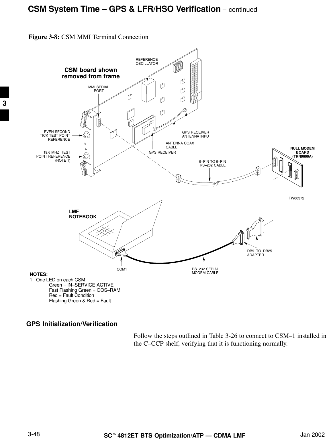
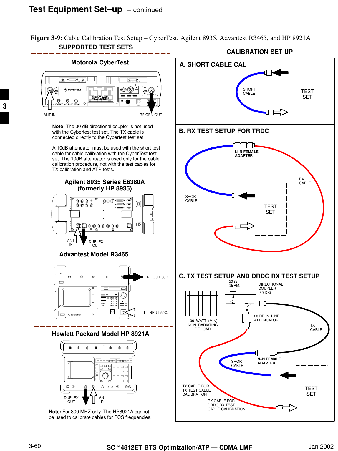
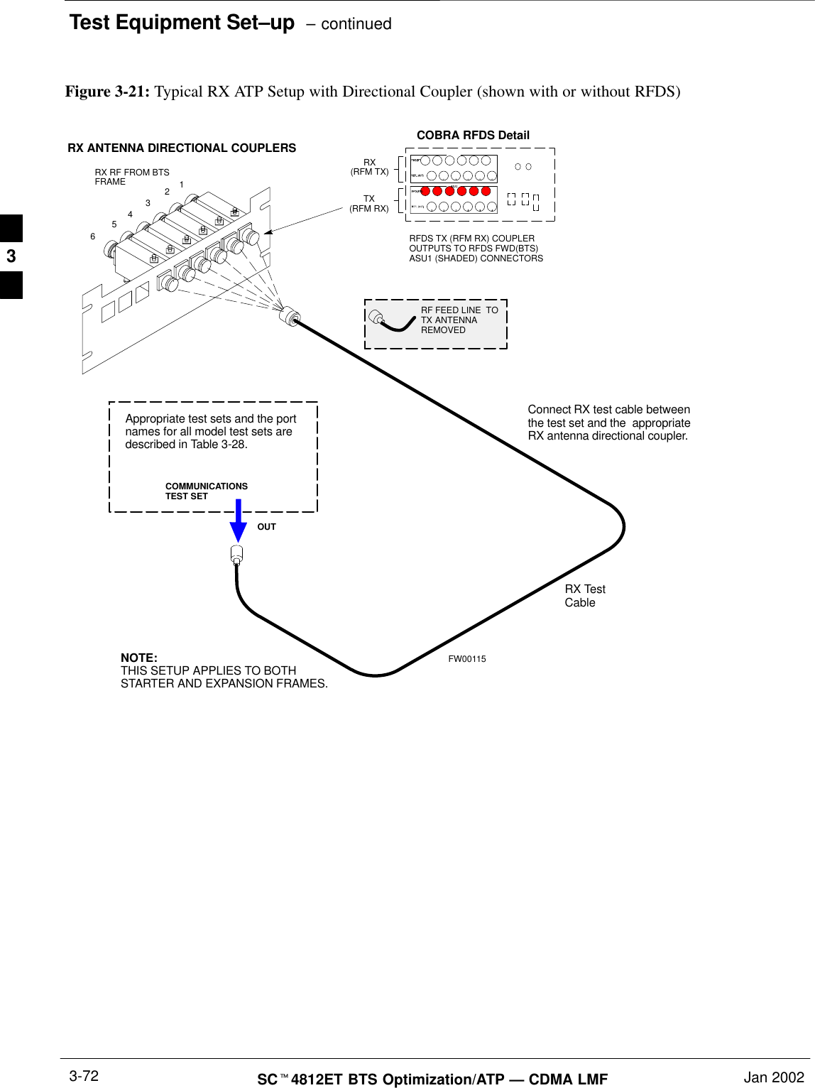
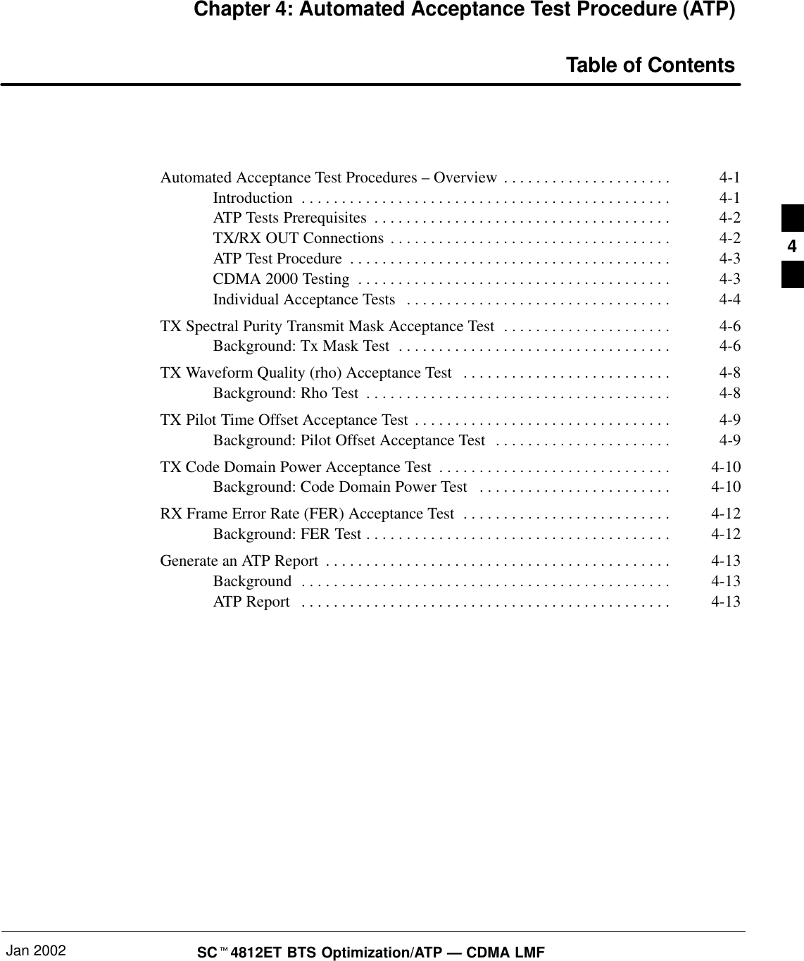
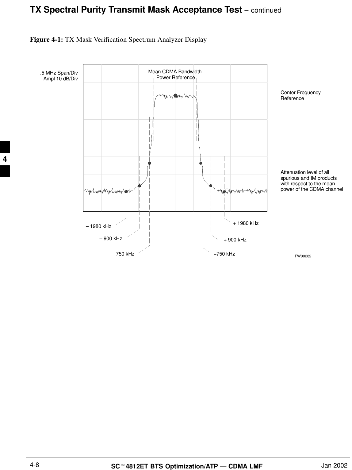
![Bay Level Offset Calibration – continuedJan 2002 3-85SCt4812ET BTS Optimization/ATP — CDMA LMFBLO Calibration Data FileDuring the calibration process, the LMF creates a calibration (BLO) datafile. After calibration has been completed, this offset data must bedownloaded to the BBXs using the Download BLO function. Anexplanation of the file is shown below.Due to the size of the file, Motorola recommends that youprint out a hard copy of a bts.cal file and refer to it for thefollowing descriptions.NOTEThe CAL file is subdivided into sections organized on a per slot basis (aslot Block).Slot 1 contains the calibration data for the 12 BBX slots. Slot 20contains the calibration data for the redundant BBX (see Table 3-39).Each BBX slot header block contains:SA creation Date and Time – broken down into separate parameters ofcreateMonth, createDay, createYear, createHour, and createMin.SThe number of calibration entries – fixed at 720 entries correspondingto 360 calibration points of the CAL file including the slot header andactual calibration data.SThe calibration data for a BBX is organized as a large flat array. Thearray is organized by branch, BBX slot, and calibration point.–The first breakdown of the array indicates which branch thecontained calibration points are for. The array covers transmit, mainreceive and diversity receive offsets as follows:Table 3-38: BLO BTS.cal file Array Branch AssignmentsRange AssignmentC[1]–C[240] TransmitC[241]–C[480] ReceiveC[481]–C[720] Diversity Receive3](https://usermanual.wiki/Nokia-Solutions-and-Networks/T5CT1.IHET5CT1-GLI2-Manual-3-of-6/User-Guide-280703-Page-56.png)
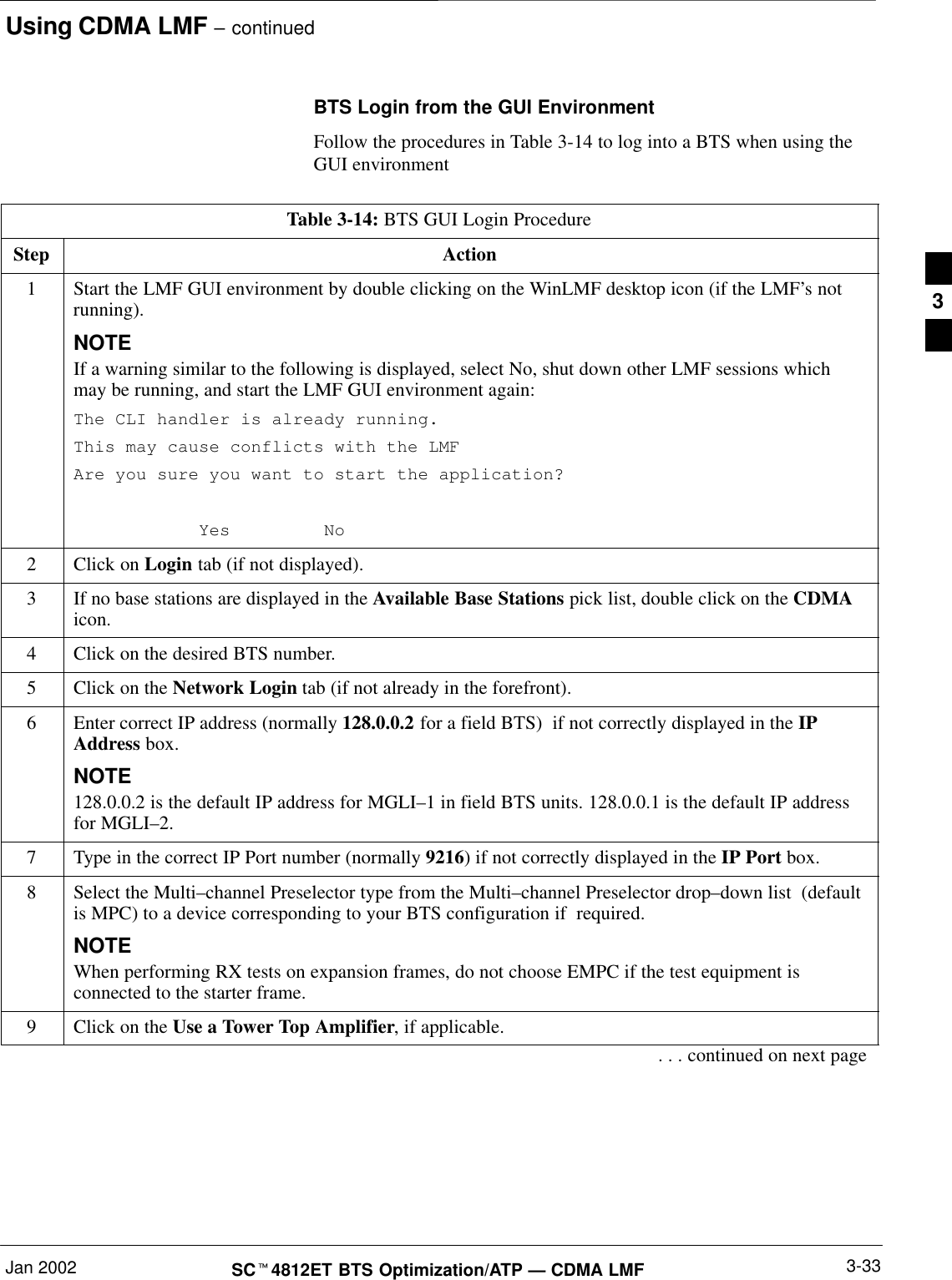
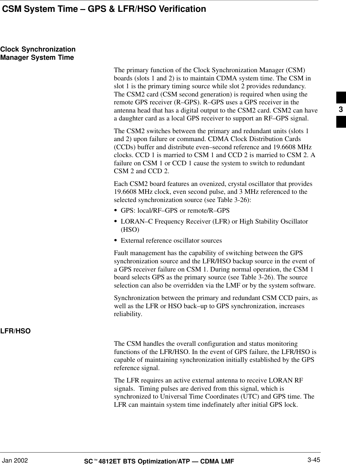
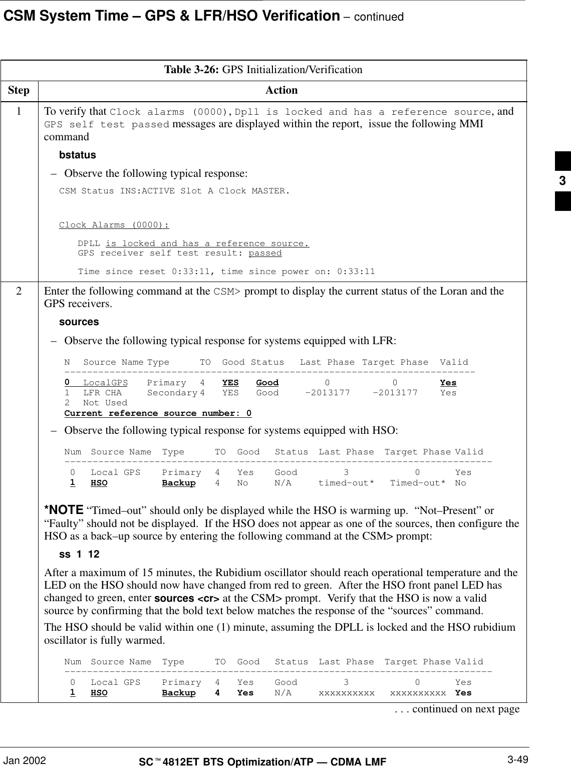
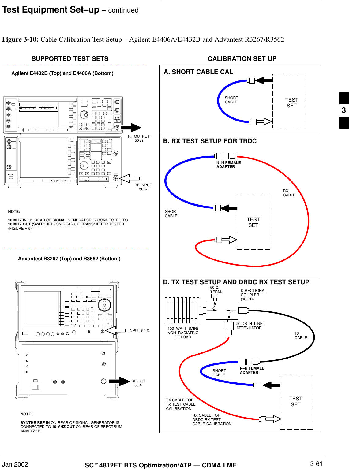
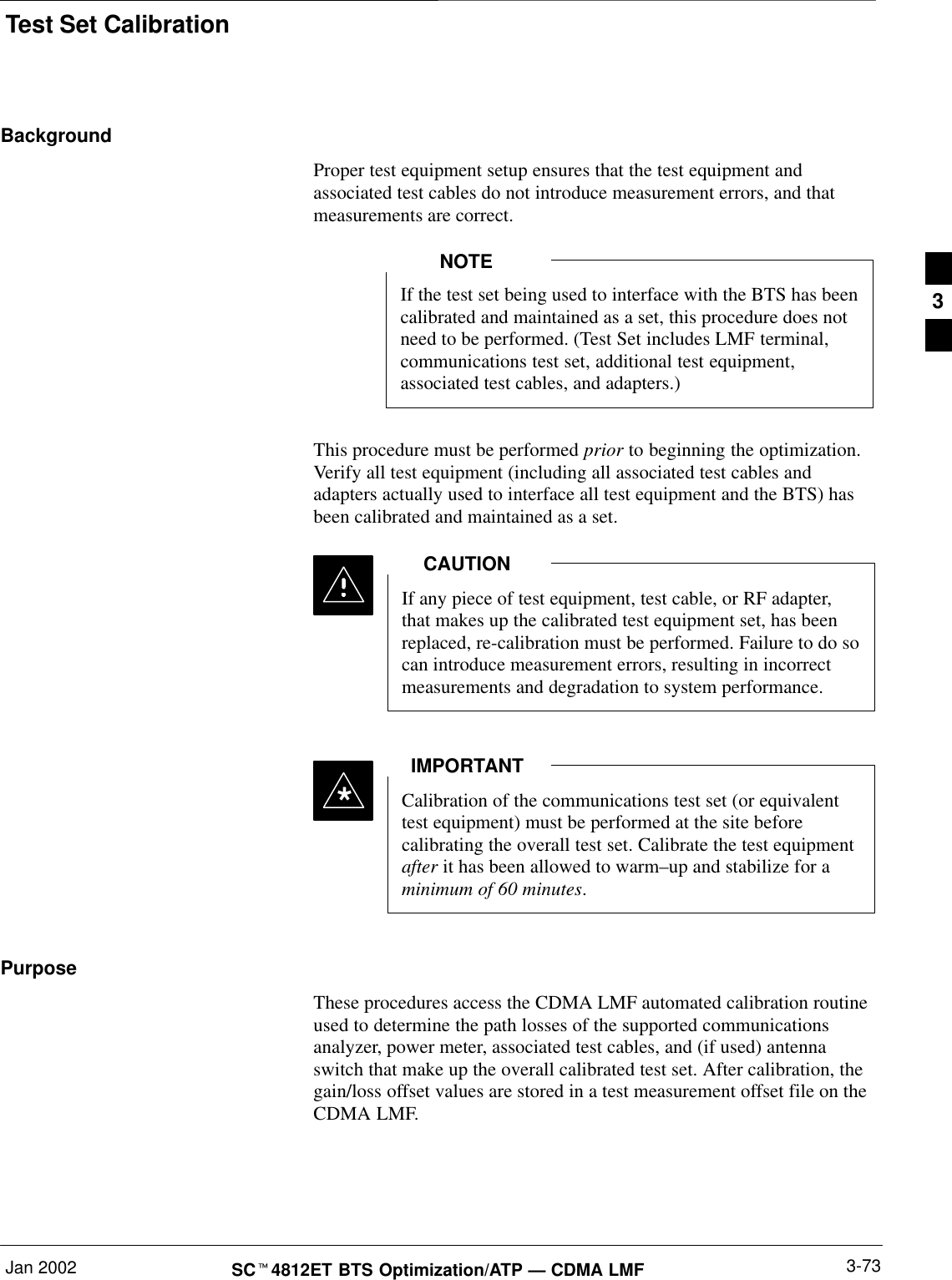
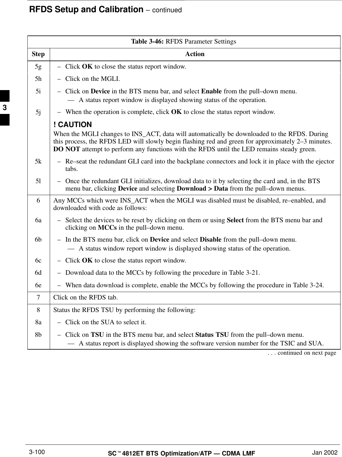
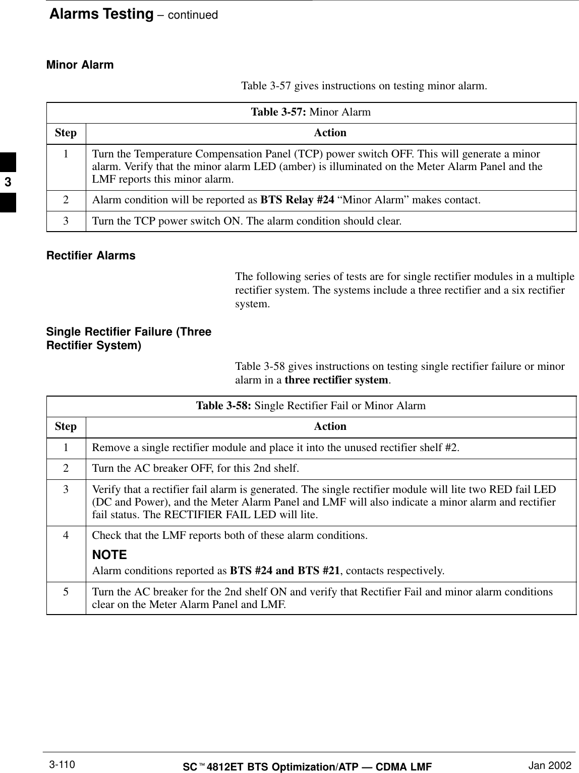
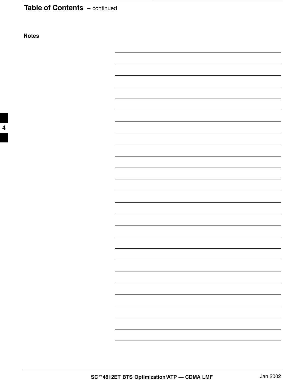
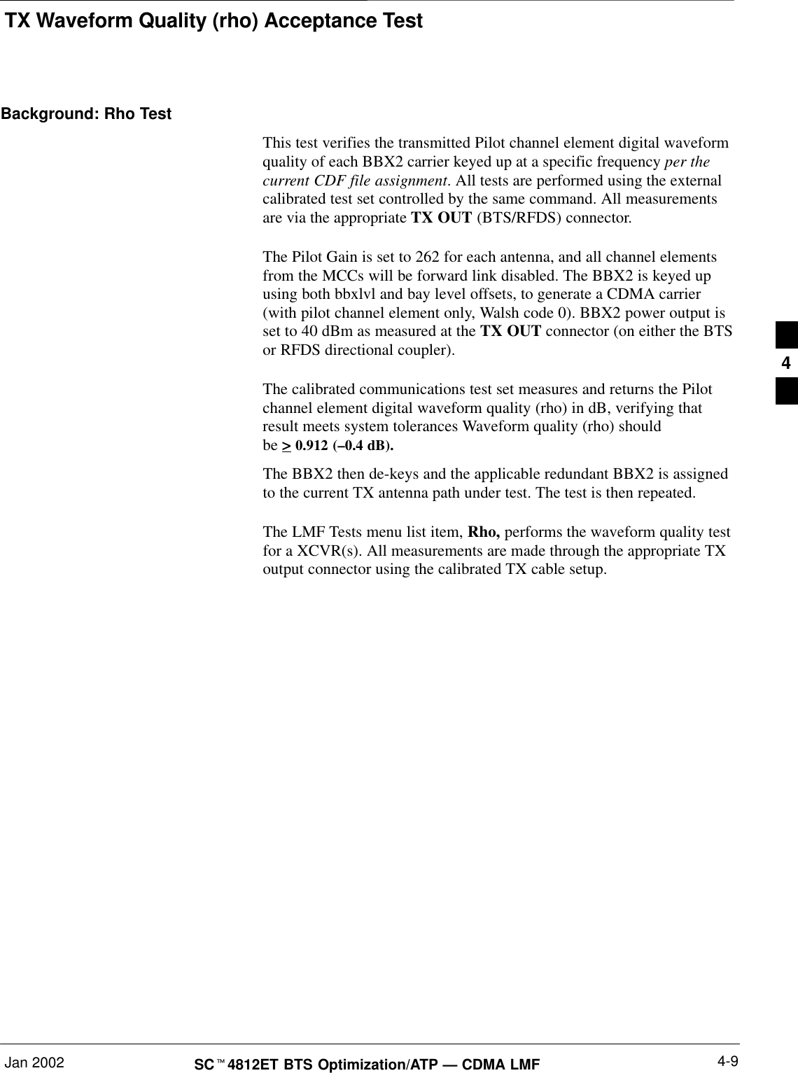
![Bay Level Offset Calibration – continuedSCt4812ET BTS Optimization/ATP — CDMA LMF Jan 20023-86–The second breakdown of the array is per sector. Three sectors areallowed.Table 3-39: BTS.cal File Array (Per Sector)BBX Sectorization TX RX RX DiversitySlot[1] (Primary BBXs 1 through 12)1 (Omni) 3–Sector, C[1]–C[20] C[241]–C[260] C[481]–C[500]23–Sector,1st C[21]–C[40] C[261]–C[280] C[501]–C[520]36 Sector, Carrier C[41]–C[60] C[281]–C[300] C[521]–C[540]41stCarrier 3–Sector, C[61]–C[80] C[301]–C[320] C[541]–C[560]5Carrier 3–Sector,3rd C[81]–C[100] C[321]–C[340] C[561]–C[580]6Carrier C[101]–C[120] C[341]–C[360] C[581]–C[600]73–Sector, C[121]–C[140] C[361]–C[380] C[601]–C[620]83–Sector,2nd C[141]–C[160] C[381]–C[400] C[621]–C[640]96 Sector, Carrier C[161]–C[180] C[401]–C[420] C[641]–C[660]10 2ndCarrier 3–Sector, C[181]–C[200] C[421]–C[440] C[661]–C[680]11 Carrier 3–Sector,4th C[201]–C[220] C[441]–C[460] C[681]–C[700]12 Carrier C[221]–C[240] C[461]–C[480] C[701]–C[720]Slot[20] (Redundant BBX–13)1 (Omni) 3–Sector, C[1]–C[20] C[241]–C[260] C[481]–C[500]23–Sector,1st C[21]–C[40] C[261]–C[280] C[501]–C[520]36 Sector, Carrier C[41]–C[60] C[281]–C[300] C[521]–C[540]41stCarrier 3–Sector, C[61]–C[80] C[301]–C[320] C[541]–C[560]5Carrier 3–Sector,3rd C[81]–C[100] C[321]–C[340] C[561]–C[580]6Carrier C[101]–C[120] C[341]–C[360] C[581]–C[600]73–Sector, C[121]–C[140] C[361]–C[380] C[601]–C[620]83–Sector,2nd C[141]–C[160] C[381]–C[400] C[621]–C[640]96 Sector, Carrier C[161]–C[180] C[401]–C[420] C[641]–C[660]10 2ndCarrier 3–Sector, C[181]–C[200] C[421]–C[440] C[661]–C[680]11 Carrier 3–Sector,4th C[201]–C[220] C[441]–C[460] C[681]–C[700]12 Carrier C[221]–C[240] C[461]–C[480] C[701]–C[720]SRefer to the hard copy of the file. As you can see, 10 calibrationpoints per sector are supported for each branch. Two entries arerequired for each calibration point.SThe first value (all odd entries) refer to the CDMA channel(frequency) the BLO is measured at. The second value (all evenentries) is the power set level. The valid range for PwrLvlAdj is from2500 to 27500 (2500 corresponds to –125 dBm and 27500corresponds to +125 dBm).3](https://usermanual.wiki/Nokia-Solutions-and-Networks/T5CT1.IHET5CT1-GLI2-Manual-3-of-6/User-Guide-280703-Page-57.png)
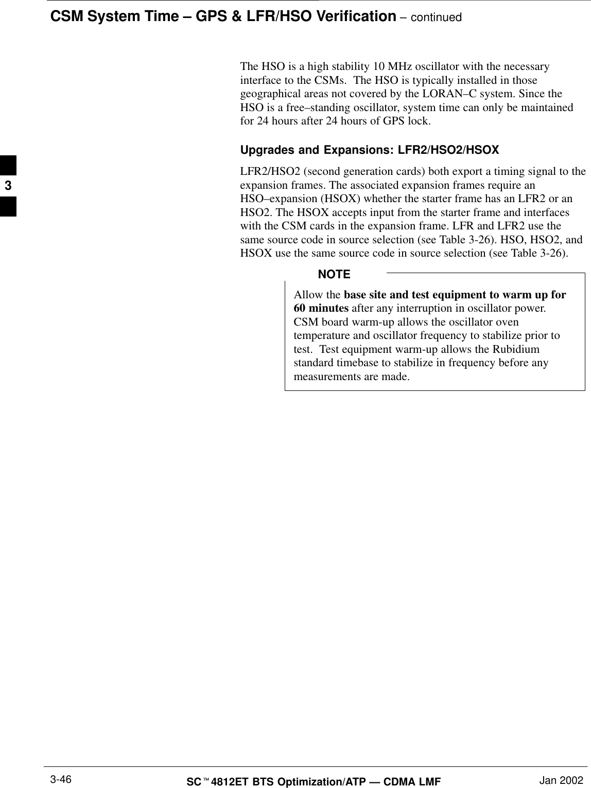
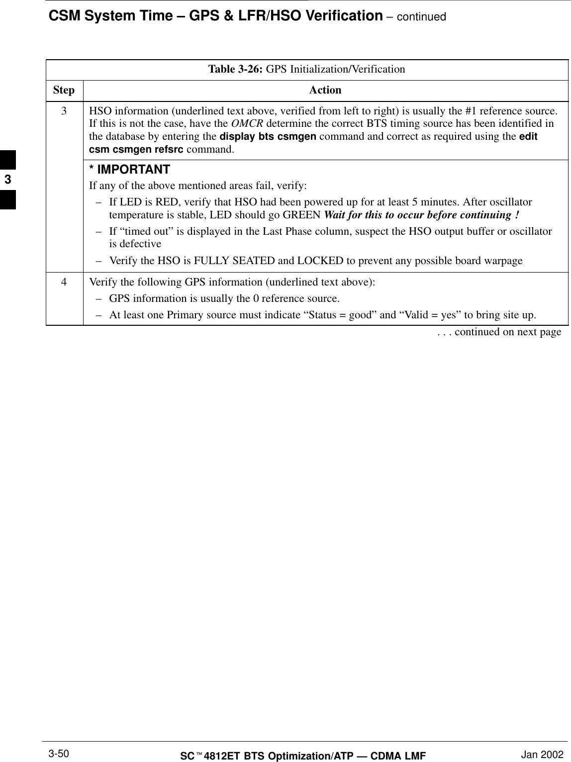
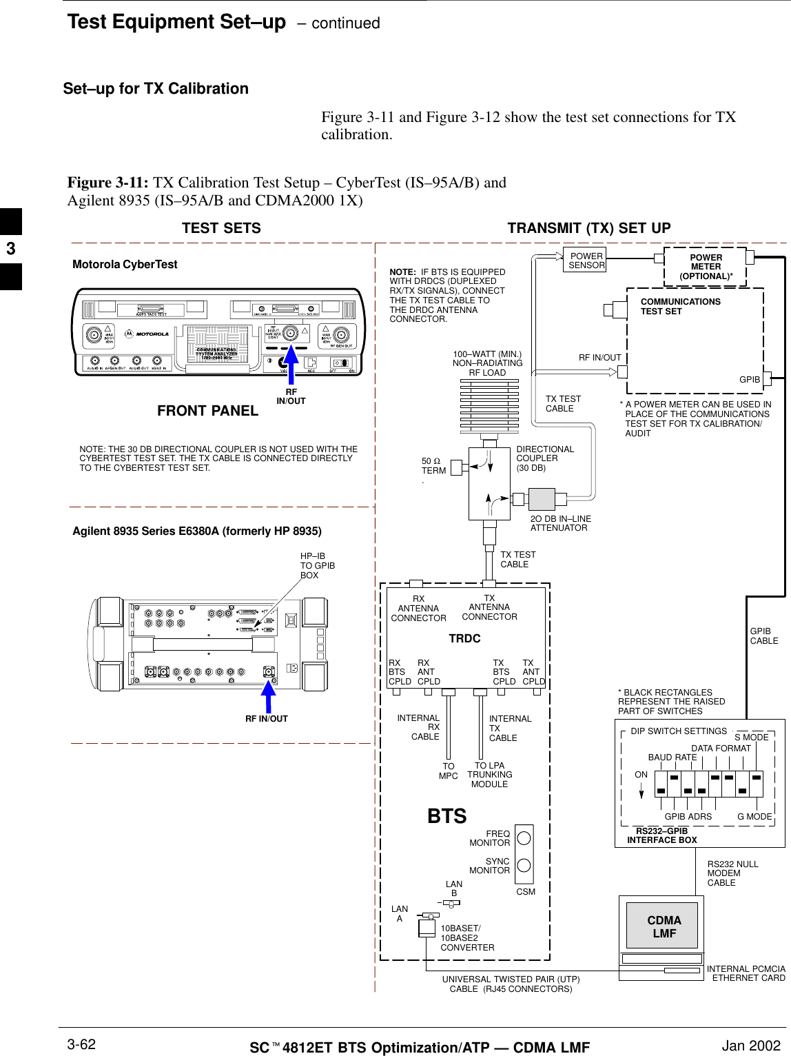
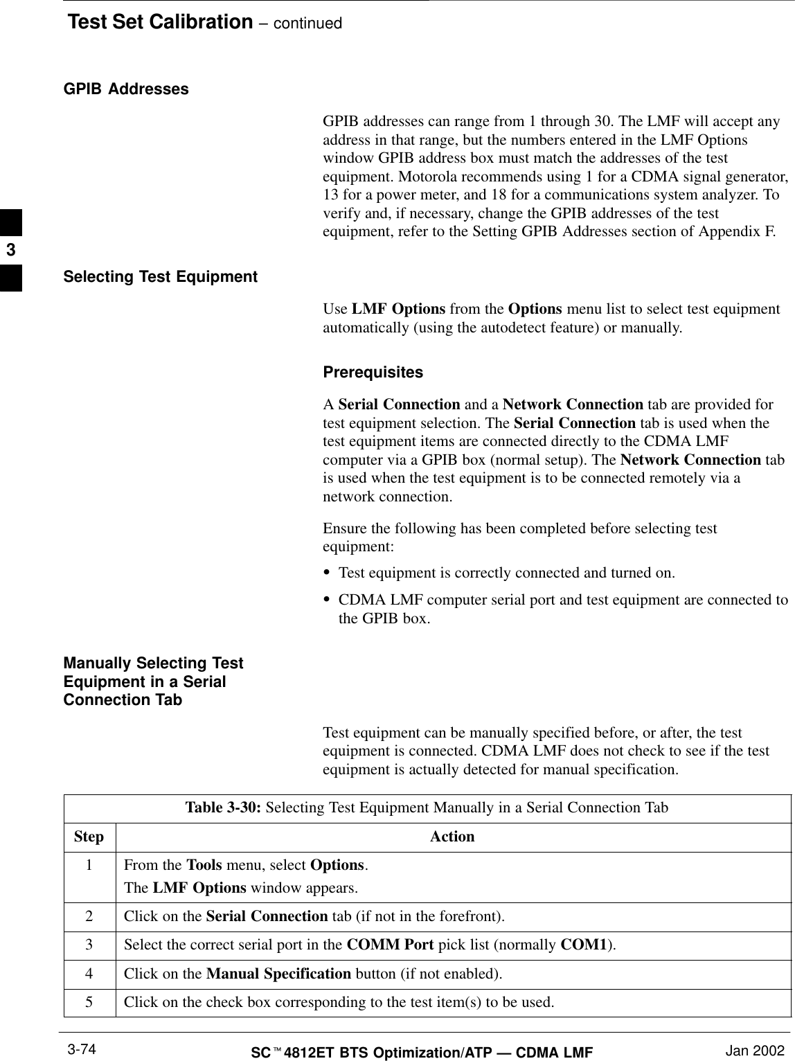
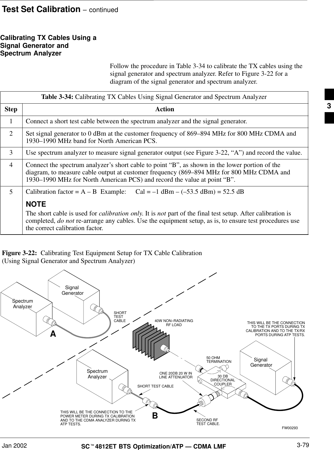
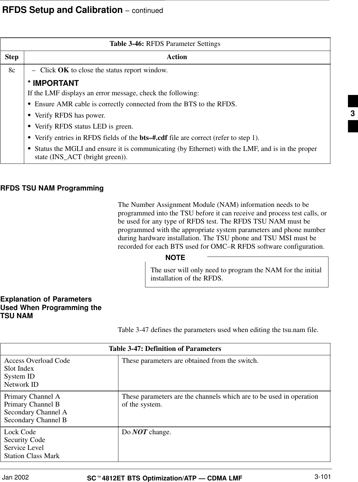
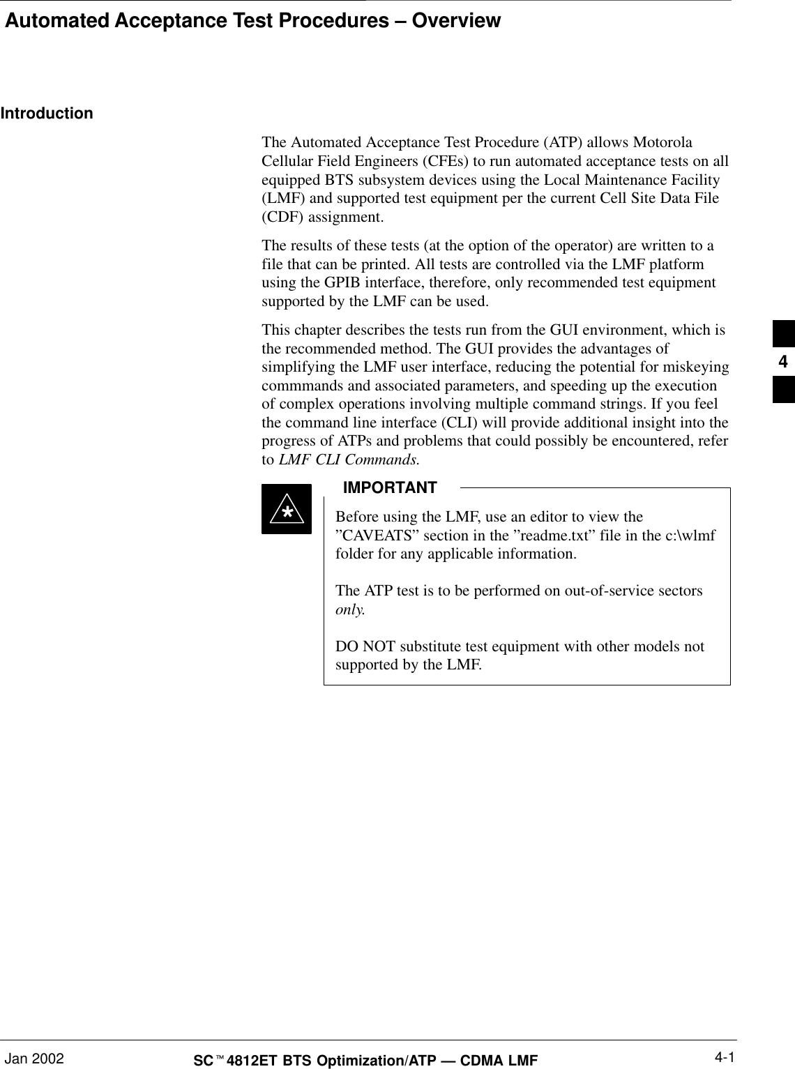
![Bay Level Offset Calibration – continuedJan 2002 3-87SCt4812ET BTS Optimization/ATP — CDMA LMFSThe 20 calibration entries for each slot/branch combination must bestored in order of increasing frequency. If less than 10 points(frequencies) are calibrated, the largest frequency that is calibrated isrepeated to fill out the 10 points.Example:C[1]=384, odd cal entry = 1 ‘‘calibration point”C[2]=19102, even cal entryC[3]=777,C[4]=19086,..C[19]=777,C[20]=19086, (since only two cal points were calibrated this would be repeated for the next 8 points)SWhen the BBX is loaded with BLO data, the cal file data for the BBXis downloaded to the device in the order it is stored in the CAL file.TxCal data is sent first, C[1] – C[60]. BBX slot 1’s 10 calibrationpoints are sent (C[1] – C[20]), followed by BBX slot 2’s 10calibration points (C[21] – C[40]), etc. The RxCal data is sent next,followed by the RxDCal data.STemperature compensation data is also stored in the cal file for eachslot.Test Equipment Setup:RF Path CalibrationFollow the steps in Table 3-40 to set up test equipment.Table 3-40: Test Equipment Setup (RF Path Calibration)Step ActionNOTEVerify the GPIB is properly connected and turned on.! CAUTIONTo prevent damage to the test equipment, all transmit (TX) test connections must be via the 30 dBdirectional coupler for 800 MHz or via a 30 dB coupler with a 20 dB in–line attenuator for 1900 MHz.1Connect the LMF computer terminal to the BTS LAN A connector on the BTS (if you have notalready done so). Refer to the procedure in Table 3-6.SIf required, calibrate the test equipment per the procedure in Table 3-32.SConnect the test equipment as shown in Figure 3-17, Figure 3-18 and Figure 3-19.3](https://usermanual.wiki/Nokia-Solutions-and-Networks/T5CT1.IHET5CT1-GLI2-Manual-3-of-6/User-Guide-280703-Page-58.png)
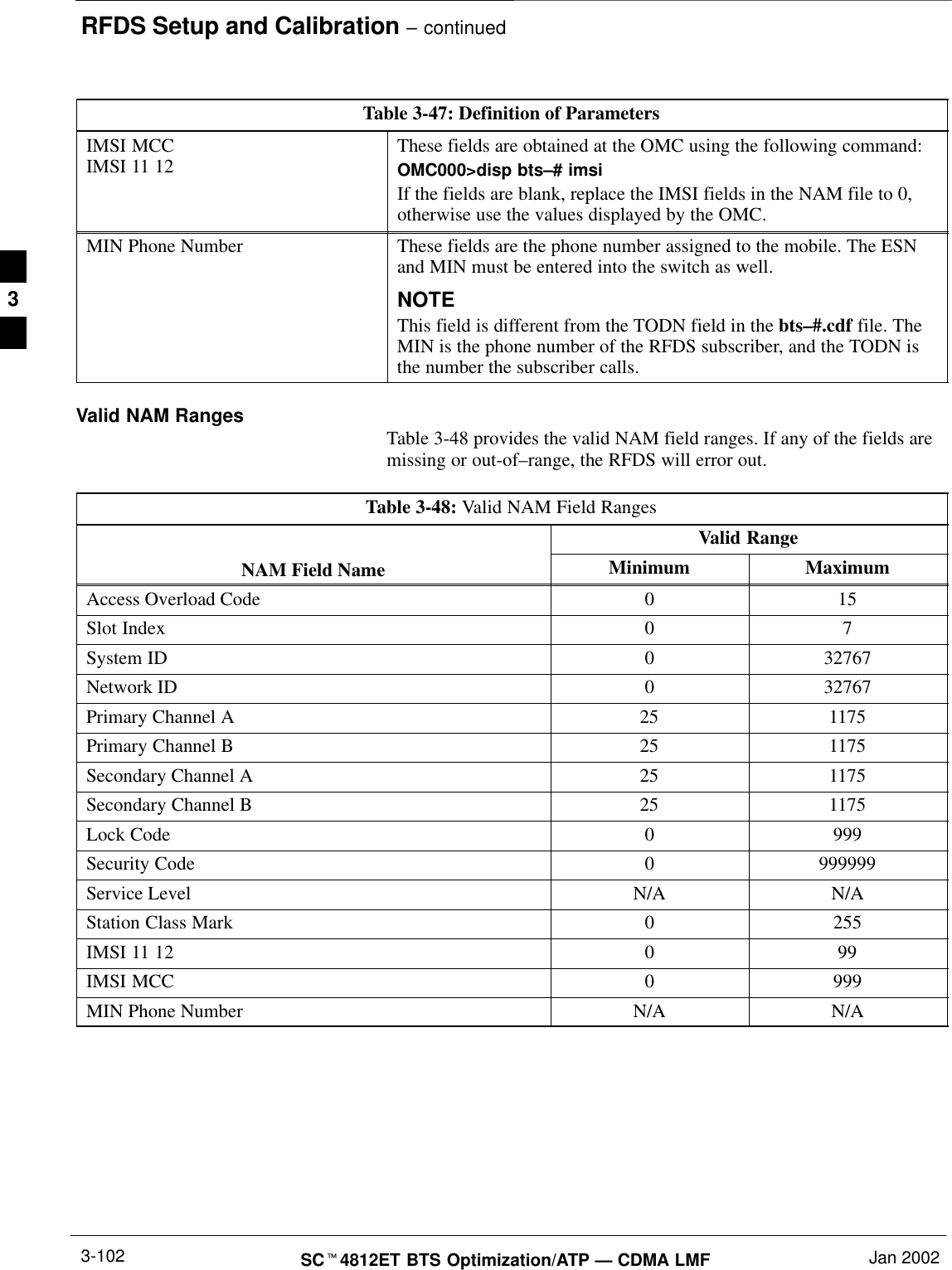
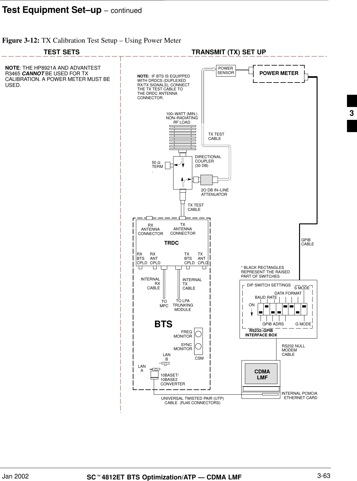
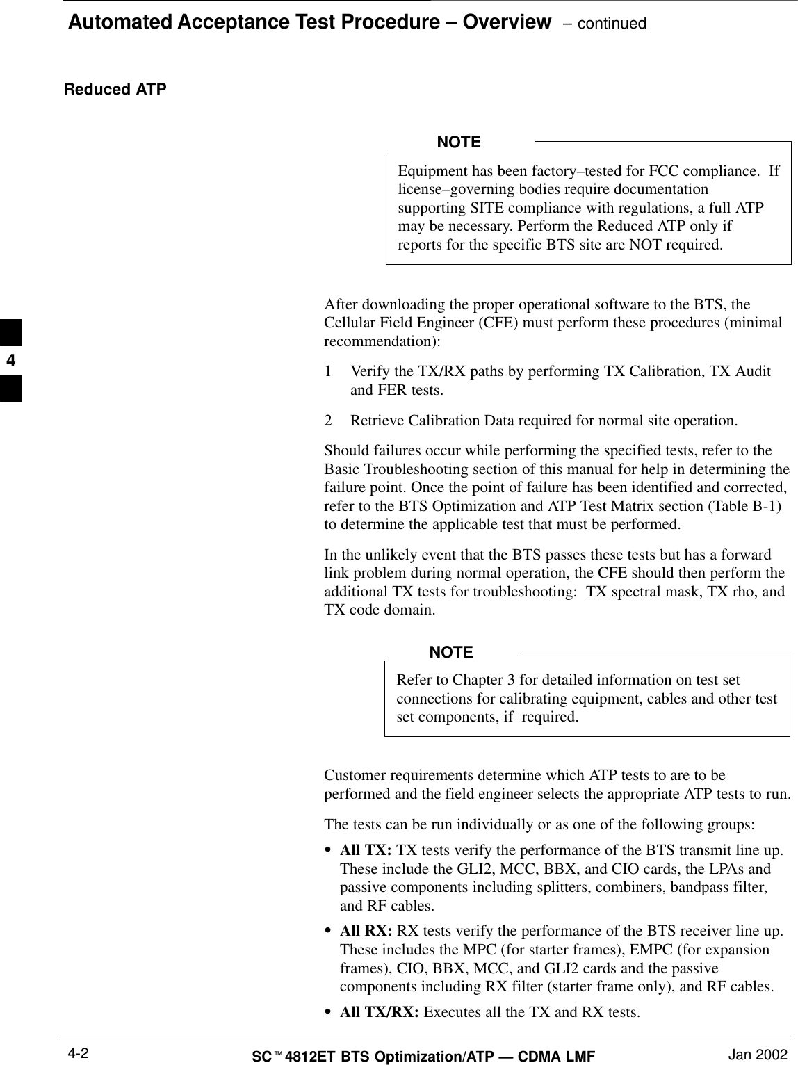
![RFDS Setup and Calibration – continuedSCt4812ET BTS Optimization/ATP — CDMA LMF Jan 20023-104Set RFDS Configuration DataIf an RFDS is installed, the RFDS configuration data must be manuallyentered.PrerequisiteSLMF is logged into the BTSThe entered antenna# index numbers must correspond tothe antenna# index numbers used in the antenna maps.IMPORTANT*Follow the procedure in Table 3-50 to set RFDS configuration data.Table 3-50: Set RFDS Configuration DataStep Action1Click on Util in the BTS menu bar, and select Edit > RFDS Configuration... from the pull–downmenus.–A tabbed data entry pop–up window will appear.2In the data entry pop–up window, click on the TX RFDS Configuration or RX RFDS Configurationtab, as required.3To add a new antenna number, perform the following:3a –Click on the Add Row button.3b –Click in the Antenna #, Cal Antenna, Scap Antenna, or Populate [Y/N] columns, as required.3c –Enter the desired data.4To edit existing values click in the data box to be changed and change the value.NOTERefer to the CDMA Help > Utility Menu > Edit–RFDS Configuration... section of LMF Helpfunction on–line documentation for RFDS configuration data examples.5To delete a row, click on the row and then click on the Delete Row button.6For each tab with changes, click on the Save button to save displayed values.7Click on the Dismiss button to close the window.NOTESValues entered or changed after the Save button was used will be lost when the window isdismissed.SEntered values will be used by the LMF as soon as they are saved. It is not necessary to log out andlog back into the LMF for changes to take effect. 3](https://usermanual.wiki/Nokia-Solutions-and-Networks/T5CT1.IHET5CT1-GLI2-Manual-3-of-6/User-Guide-280703-Page-75.png)
![RFDS Setup and Calibration – continuedJan 2002 3-105SCt4812ET BTS Optimization/ATP — CDMA LMFRFDS CalibrationThe RFDS Calibration option is used to calibrate the RFDS TX and RXpaths.TX Path Calibration – For a TX antenna path calibration the BTSXCVR is keyed at a pre–determined power level and the BTS poweroutput level is measured by the RFDS. The power level is then measuredat the TX antenna directional coupler by the power measuring testequipment item being used (power meter or analyzer). The difference(offset) between the power level at the RFDS and the power level at theTX antenna directional coupler is used as the TX RFDS calibrationoffset value.RX Path Calibration – For an RX antenna path calibration the RFDS iskeyed at a pre–determined power level and the power input level ismeasured by the BTS BBX. A CDMA signal at the same power levelmeasured by the BTS BBX is then injected at the RX antenna directionalcoupler by the communications system analyzer. The difference (offset)between the RFDS–keyed power level and power level measured at theBTS BBX is the RFDS RX calibration offset value.RFDS calibration and the CAL file – The TX and RX RFDScalibration offset values are written to the CAL file in the slot[385]Block.TSIC channel frequency – For each RFDS TSIC, the channelfrequency is determined at the lower third and upper third of theappropriate band using the frequencies listed in Table 3-51.Table 3-51: RFDS TSIC Calibration Channel FrequenciesSystem Channel Calibration Points800 MHz (A and B) 341 and 6821.9 GHz 408 and 791Before installing any test equipment directly to any TXOUT connector, verify that there are no CDMA channelskeyed. Failure to do so can result in serious personal injuryand/or equipment damage.WARNINGRFDS Calibration ProcedurePrerequisitesSTest equipment has been selected.STest equipment and test cables have been calibrated.STX calibration has been performed and BLO data has beendownloaded to the BBXs.3](https://usermanual.wiki/Nokia-Solutions-and-Networks/T5CT1.IHET5CT1-GLI2-Manual-3-of-6/User-Guide-280703-Page-76.png)
![Automated Acceptance Test Procedure – Overview – continuedSCt4812ET BTS Optimization/ATP — CDMA LMF Jan 20024-6ATP Test Procedure Table 4-1 describes the step–by–step procedures to run any APT Test.Table 4-1: ATP Test ProcedureStep Action1Select the device(s) to be tested.2From the Tests menu, select the desired test.3Select the appropriate carrier(s) (carrier – bts# – sector# – carrier#) displayed in the Channels/Carrierpick list.To select multiple items, hold down the <Shift> or <Ctrl> key while making the selections.4Type the appropriate channel number in the Carrier n Channels box.The default channel number displayed is determined by the CdmaChans[n] number in the cbsc–n.cdffile for the BTS.5If applicable, select Verify BLO (default) or Single–sided BLO.NOTESingle–sided BLO is only used when checking non–redundant transceivers.6For RX select the appropriate RX branch (Both, Main, or Diversity) in the drop–down list.7In the Rate Set box, select the appropriate data rate (1=9600, 2=14400, 3=9600 1X) from thedrop–down list.NOTEThe Rate Set selection of 3 is only available if 1X cards are selected for the test.8In the Test Pattern box, select the test pattern to use for the calibration from the drop–down list: Pilot(default), CDF, CDFPilot or Standard.9 Click OK.The status report window and a Directions pop-up are displayed.10 Follow the cable connection directions as they are displayed.11 Click Save Results or Dismiss to close the status report window. If Dismiss is used the test results will not be saved in the test report file. 4](https://usermanual.wiki/Nokia-Solutions-and-Networks/T5CT1.IHET5CT1-GLI2-Manual-3-of-6/User-Guide-280703-Page-95.png)
![RX Frame Error Rate (FER) Acceptance TestJan 2002 4-13SCt4812ET BTS Optimization/ATP — CDMA LMFBackground: FER TestThis test verifies the BTS FER on all traffic channel elements currentlyconfigured on all equipped MCCs (full rate at 1% FER) at an RF inputlevel of –119 dBm [or –116 dBm if using Tower Top Amplifier(TMPC)]. All tests are performed using the external calibrated test set asthe signal source controlled by the same command. All measurementswill be via the LMF.The pilot gain is set to 262 for each TX antenna and all channel elementsfrom the MCCs are forward-link disabled. The BBX2 is keyed up usingonly bbxlvl level offsets, to generate a CDMA carrier (with pilot channelelement only). BBX2 power output is set to –20 dBm as measured at theTX OUT connector (on either the BTS or RFDS directional coupler).The BBX2 must be keyed in order to enable the RX receive circuitry.The LMF prompts the MCC/CE under test to measure all zero longcodeand provide the FER report on the selected active MCC on the reverselink for both the main and diversity RX antenna paths, verifying theresults meet the following specification: FER returned less than 1% andtotal frames measured is 1500.All MCC/CEs selected are tested on the specified RX antenna path. TheBBX then de-keys and, the applicable redundant BBX2 is assigned tothe current RX antenna paths under test. The test is then repeated.4](https://usermanual.wiki/Nokia-Solutions-and-Networks/T5CT1.IHET5CT1-GLI2-Manual-3-of-6/User-Guide-280703-Page-102.png)