Nokia Solutions and Networks T5CT1 Cellular CDMA base station User Manual IHET5CT1 GLI2 Manual 2 of 6
Nokia Solutions and Networks Cellular CDMA base station IHET5CT1 GLI2 Manual 2 of 6
Contents
- 1. IHET5CT1 GLI2 Manual 1 of 6
- 2. IHET5CT1 GLI2 Manual 2 of 6
- 3. IHET5CT1 GLI2 Manual 3 of 6
- 4. IHET5CT1 GLI2 Manual 4 of 6
- 5. IHET5CT1 GLI2 Manual 5 of 6
- 6. IHET5CT1 GLI2 Manual 6 of 6
- 7. IHET5CT1 GLI3 Manual 1 of 6
- 8. IHET5CT1 GLI3 Manual 4 of 6
- 9. IHET5CT1 GLI3 Manual 5 of 6
- 10. IHET5CT1 GLI3 Manual 6 of 6
IHET5CT1 GLI2 Manual 2 of 6
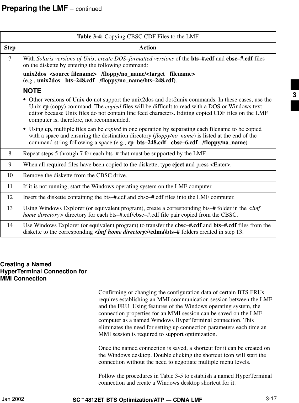
![Preparing the LMF – continuedJan 2002 3-29SCt4812ET BTS Optimization/ATP — CDMA LMFUpdate BTS Specific CDF File DeviceLoad Version and Site Type Follow the steps outlined in Table 3-12 to update the existing BTSspecific CDF file NextLoad parameter, to reflect the current device loadversion to be downloaded and verify the correct Site Type. (This is aninterim procedure and is subject to change).Device load version in the CDF file must match the currentversion loaded at the OMCR/CBSC.CAUTIONTable 3-12: Update BTS Specific CDF File Device Load VersionStep Action! CAUTIONIf you are not familiar with the UNIX vi editor, create a “dummy” CDF file, and practice makingchanges to it, prior to altering the “real” one.* IMPORTANTCDF files obtained from the OMCR.CBSC are modified by DELTA information being appended tothe end of the CDF file. The information in the DELTA fields take precedence over information in the“core CDF file” For example: If NextLoad=‘‘1.2.3.4.5” for BBX 1 was specified in the CDF file, andthere was a DELTA entry specifying NextLoad=‘‘2.3.4.5.6” appended to the CDF file for the sameBBX, 2.3.4.5.6 would be the version used.There are two ways resolve this. Edit both the DELTA and “core” areas of the file to reflect the sameversion, or make sure the delta information is transferred to the main CDF file and delete all DELTACDF file entries.1Globally change the device load version number in the new CDF file using the following UNIXcommands:vi bts–new_<bts#>.cdf:1,$ s/x.x.x.x.x/y.y.y.y.yWhere: x.x.x.x.x and y.y.y.y.y represent the old and new version number, respectively.:wqNOTEYou should now be able to download all devices at the BTS with the current device load version.2Verify the SiteType and SSType entries in the CDF file (under the BTS subheading) reflect thefollowing information. See example of applicable fields of CDF file below.(CDMA only; 1900 MHz example shown):BTS[#] = {....,SiteType=3,SSType=16...},Valid SiteTypes (SC9600=1, SC9600(Mixed)=2, SC2400=3, SC2400(Mixed)=4, SC600=5)Valid SSTypes (CDMA800MHz=8, CDMA1900MHz=16, CDMA900MHz=32)3](https://usermanual.wiki/Nokia-Solutions-and-Networks/T5CT1.IHET5CT1-GLI2-Manual-2-of-6/User-Guide-280702-Page-52.png)