Nokia Solutions and Networks T5BR1 CDMA Cellular Base Station User Manual IHET5BR1 Part 2 of 3
Nokia Solutions and Networks CDMA Cellular Base Station IHET5BR1 Part 2 of 3
Contents
- 1. IHET5BR1 User Manual Part 1 of 3
- 2. IHET5BR1 User Manual Part 2 of 3
- 3. IHET5BR1 User Manual Part 3 of 3
IHET5BR1 User Manual Part 2 of 3
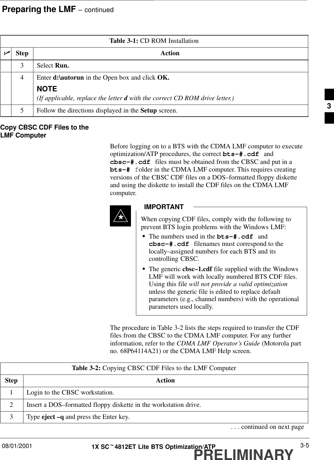
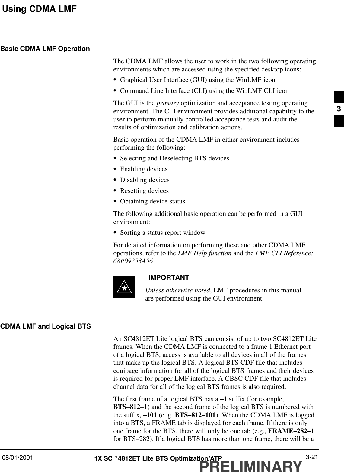
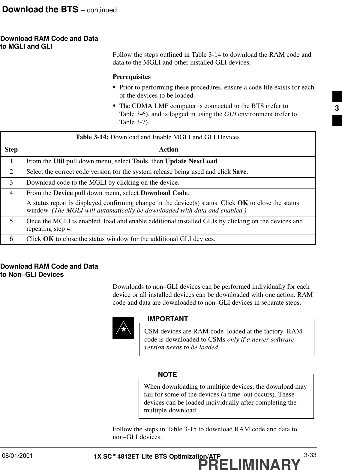
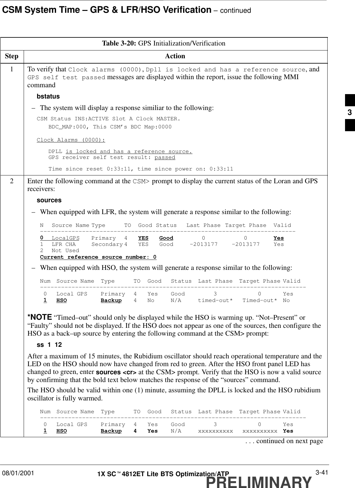
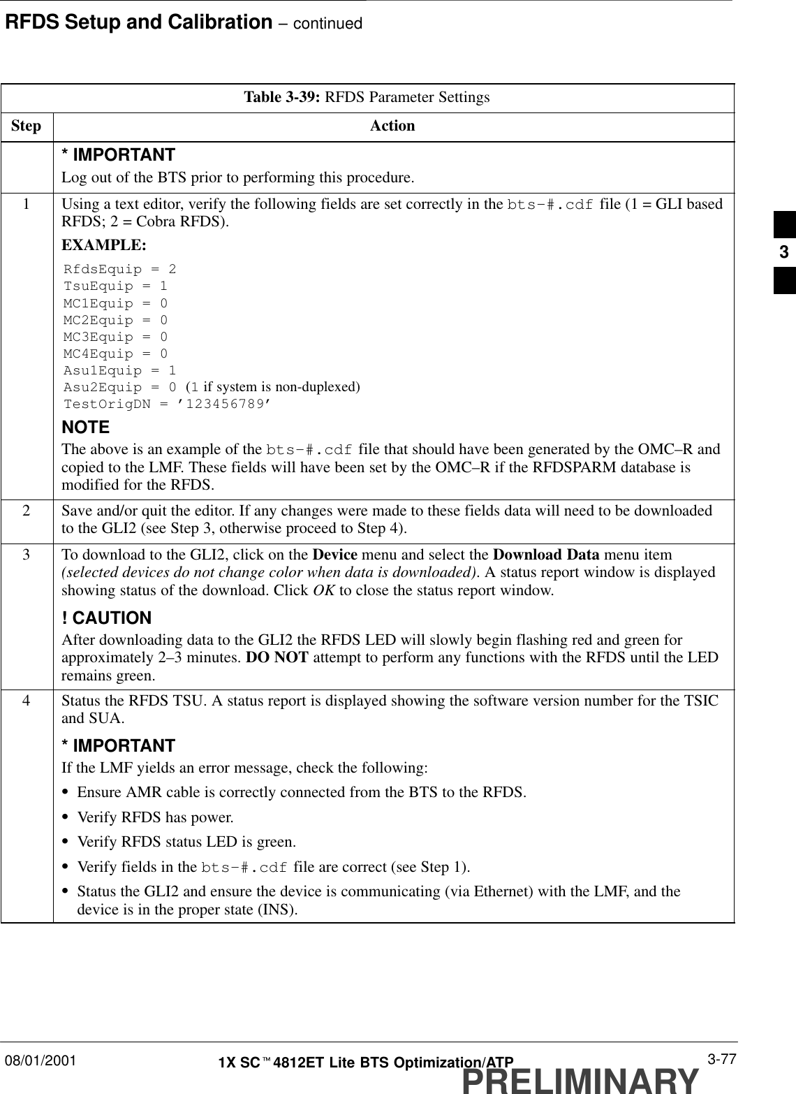
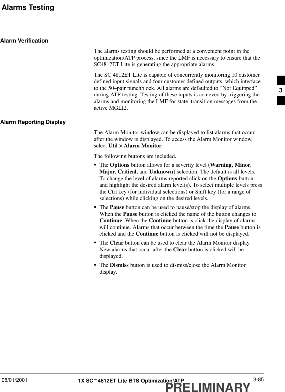
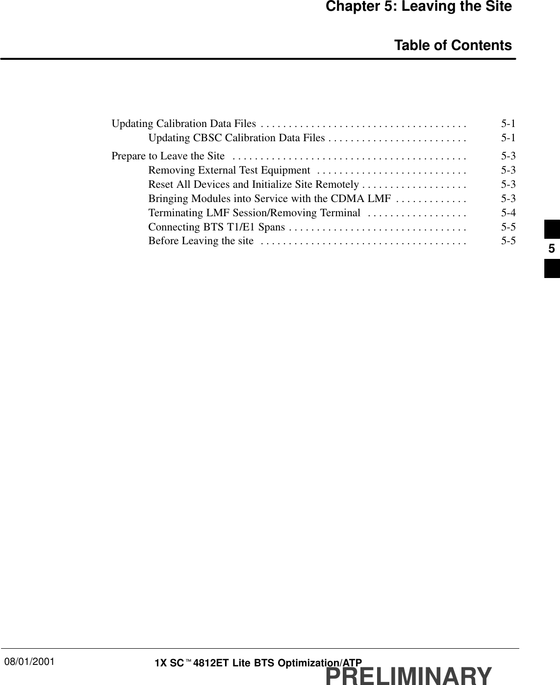
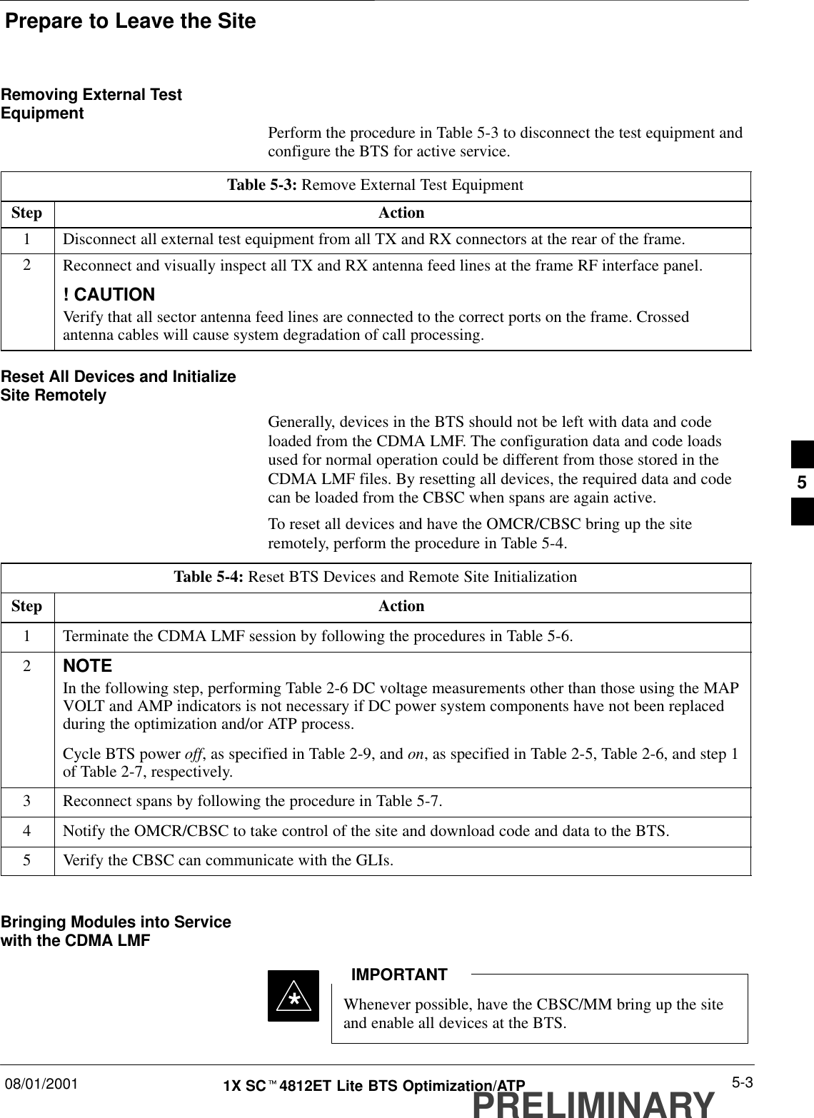
![Bay Level Offset Calibration – continuedPRELIMINARY1X SCt4812ET Lite BTS Optimization/ATP 08/01/20013-66BLO Calibration Data FileDuring the calibration process, the CDMA LMF creates a calibration(CAL) data file where BLO values are stored. After calibration has beencompleted, this offset data must be downloaded to the BBX2s using theCDMA LMF Download BLO function. An explanation of the file isshown below.Due to the size of the file, Motorola recommends printingout a copy of a bts.cal file and referring to it for thefollowing descriptions.NOTEThe CAL file is subdivided into sections organized on a per–slot basis (aslot Block).The Slot 1 Block contains the calibration data for the six BBX2 slots.The Slot 20 Block contains the calibration data for the redundant BBX2(see Table 3-32). Each BBX2 slot Block header contains:SA creation Date and Time – broken down into separate parameters ofcreateMonth, createDay, createYear, createHour, and createMin.SThe number of calibration entries – fixed at 720 entries correspondingto 360 calibration points of the CAL file – plus the slot Block format.Within the slot Block body, the BBX2 calibration data (BayLevelCal) isorganized as a large flat array. The array is organized by branch, BBX2SCCP cage slot, and calibration point.SThe first breakdown of the array indicates which branch the containedcalibration points are for. The array covers transmit, main receive, anddiversity receive offsets as follows:Table 3-31: BLO BTS.cal file Array Branch AssignmentsRange Branch AssignmentC[1]–C[120] TransmitC[121]–C[240] No SC4812ET Lite BLO calpoint entries (default only)C[241]–C[360] ReceiveC[361]–C[480] No SC4812ET Lite BLO calpoint entries (default only)C[481]–C[600] Diversity ReceiveC[601]–C[720] No SC4812ET Lite BLO calpoint entries (default only)3](https://usermanual.wiki/Nokia-Solutions-and-Networks/T5BR1.IHET5BR1-User-Manual-Part-2-of-3/User-Guide-170603-Page-64.png)
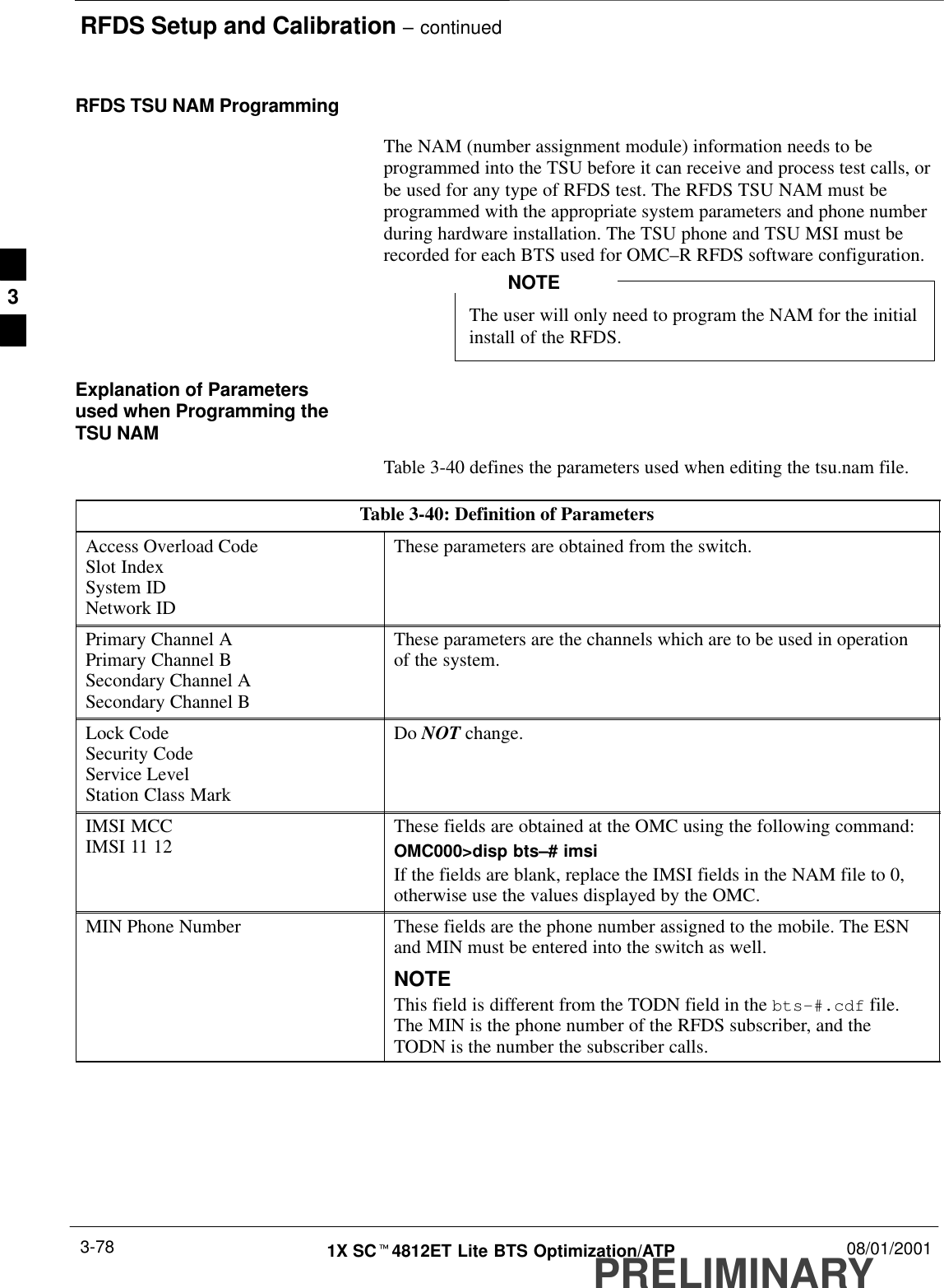
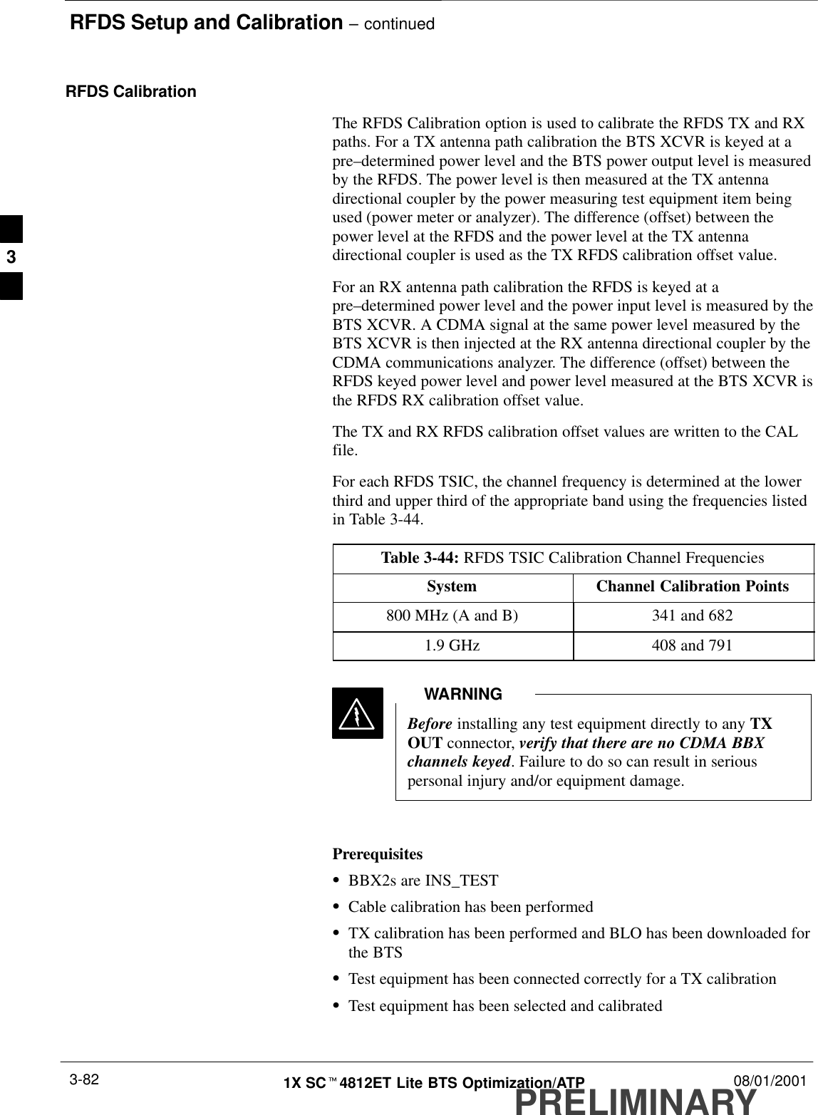
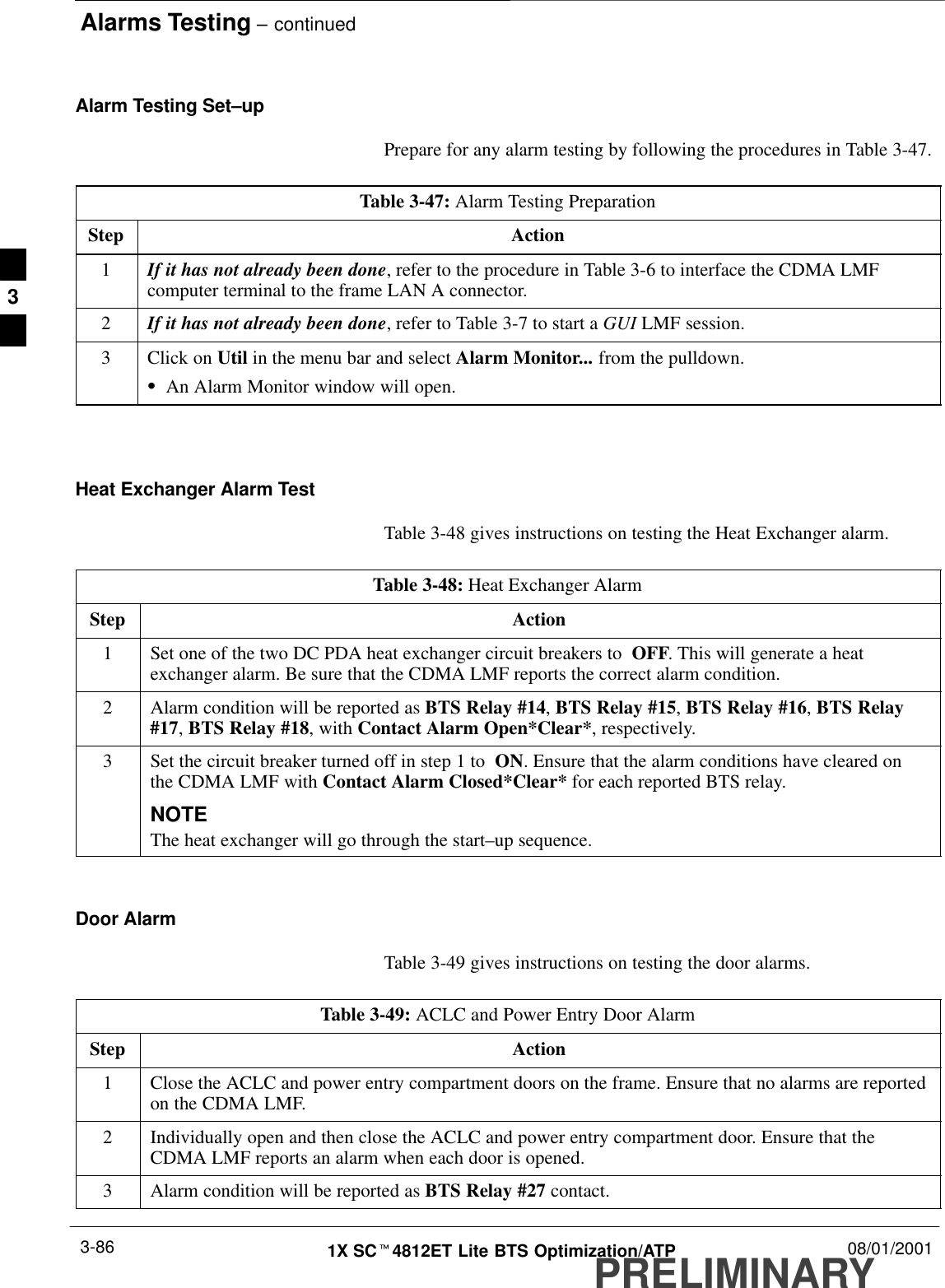
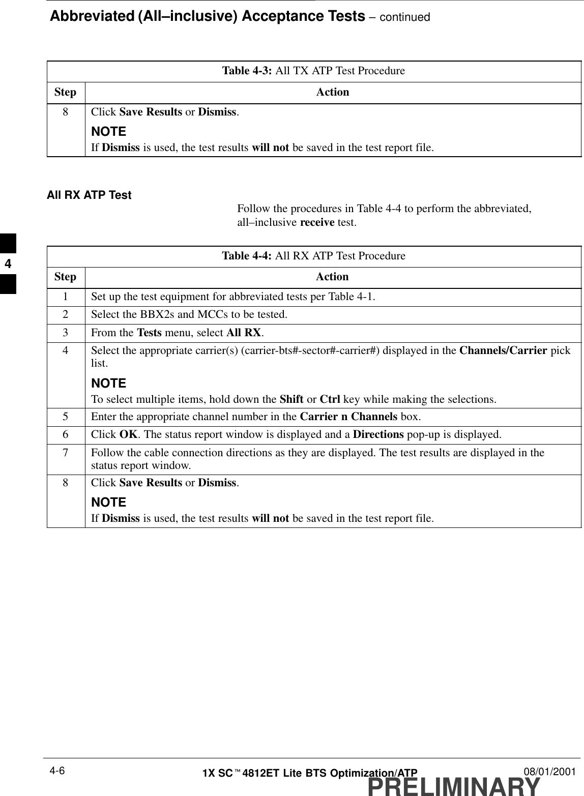
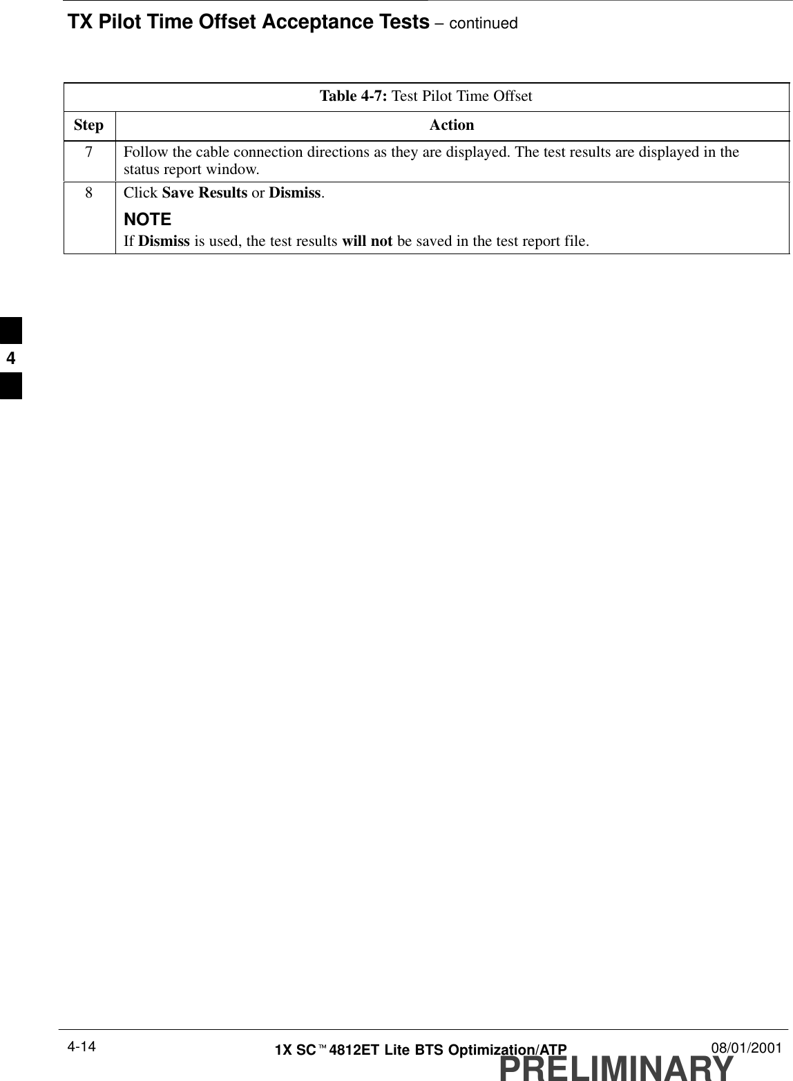
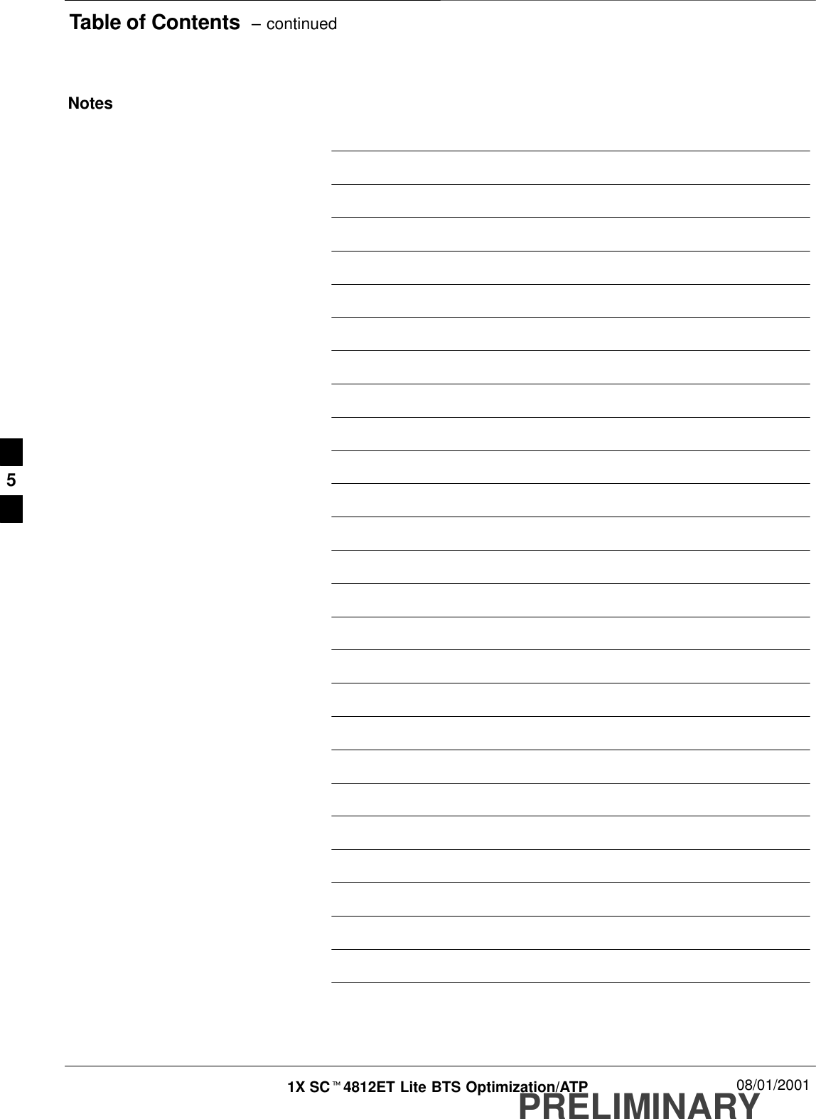
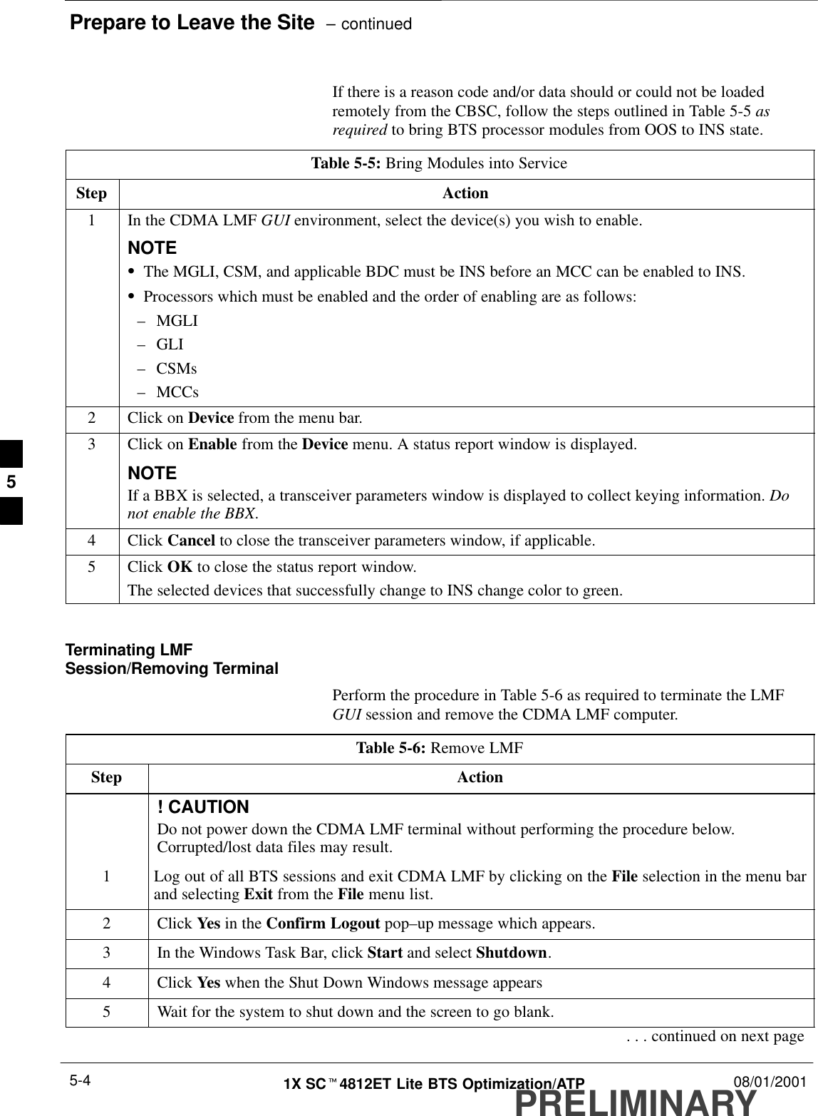
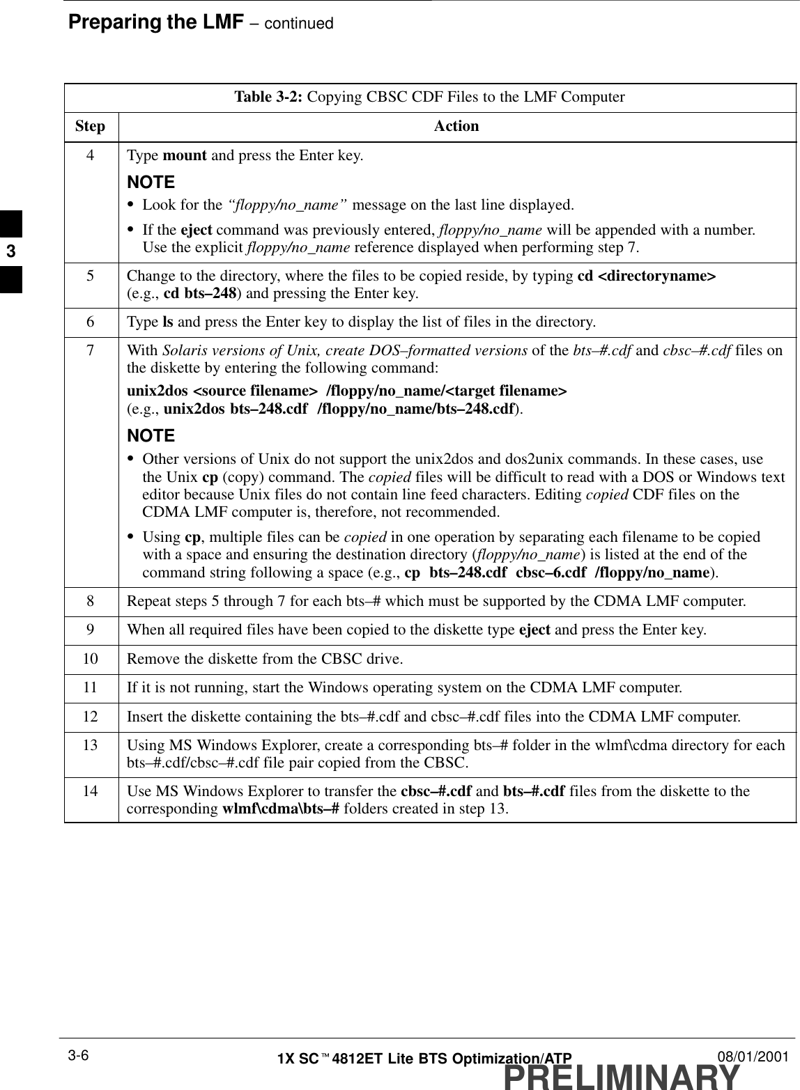
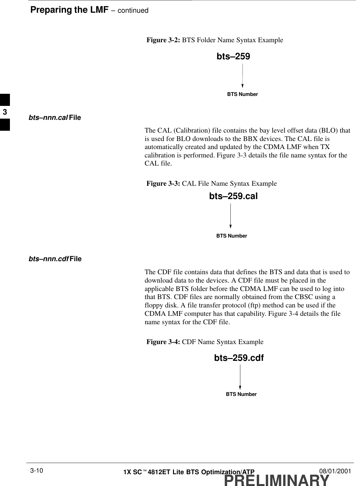
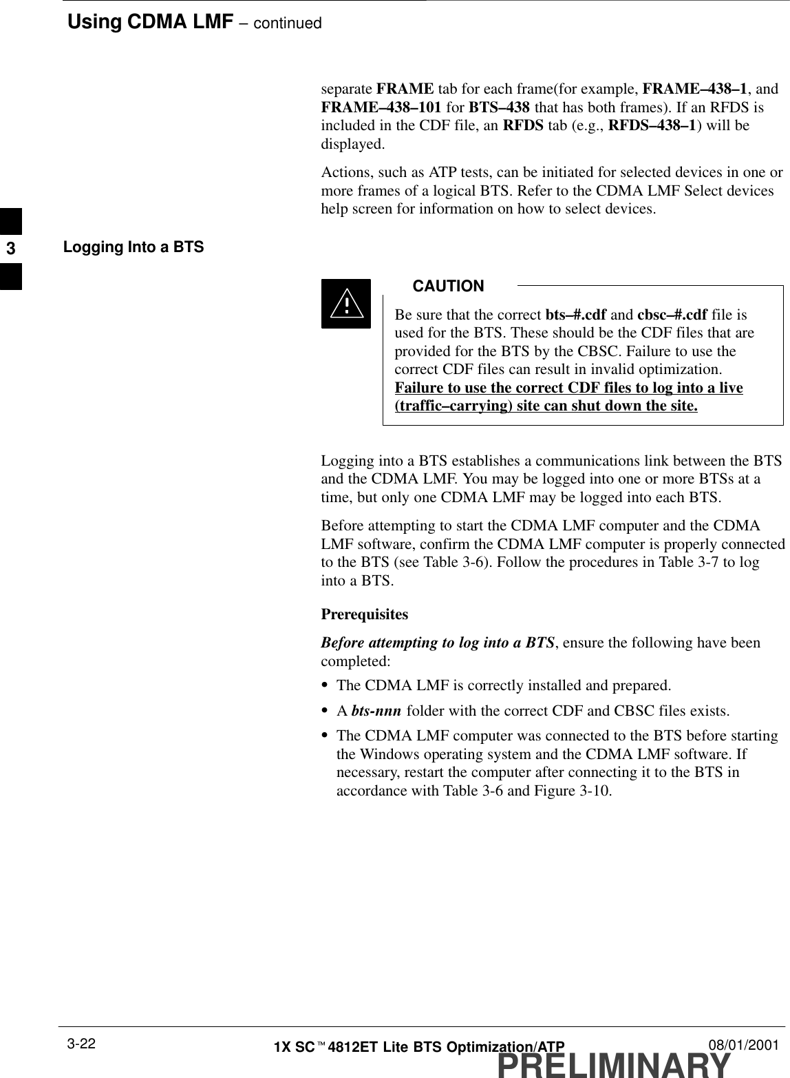
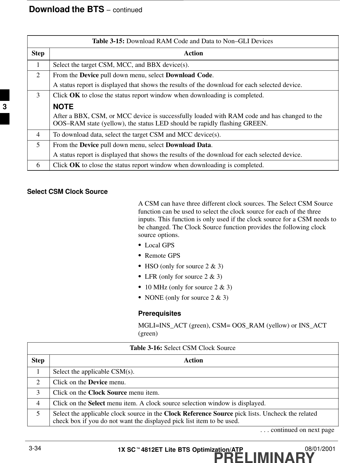
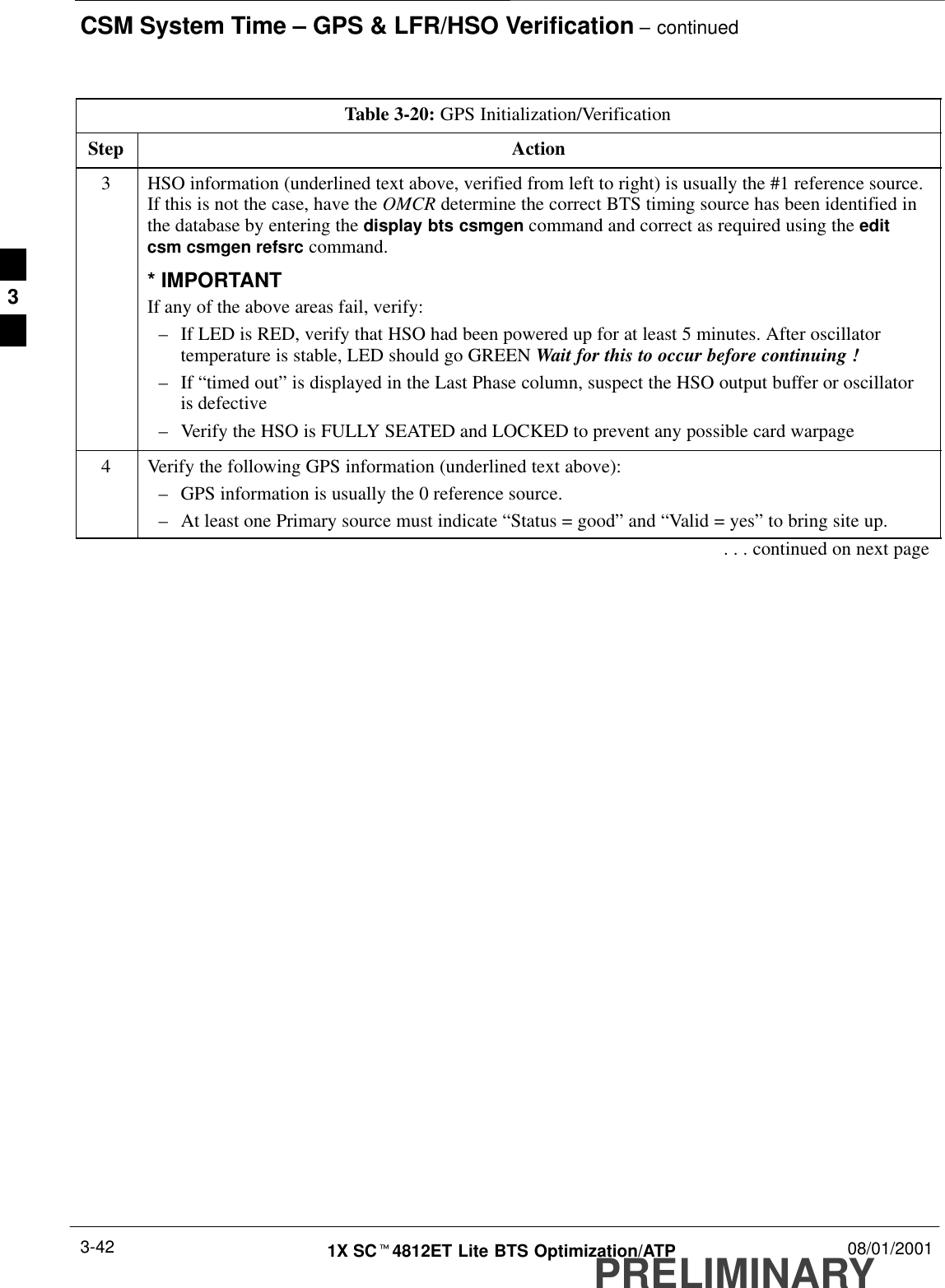
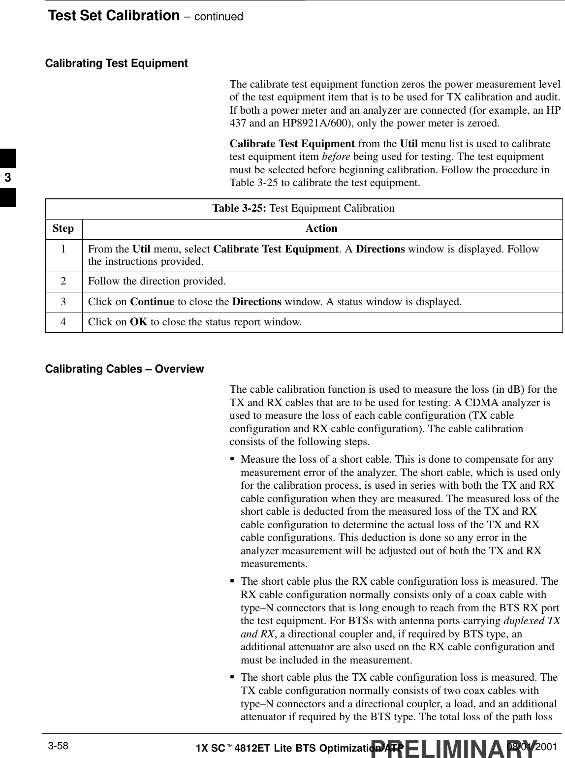
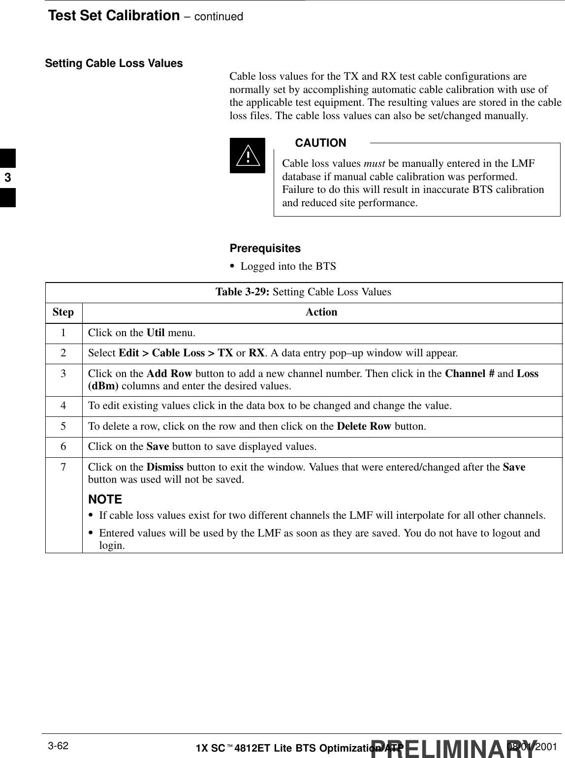
![Bay Level Offset Calibration – continued08/01/2001 3-671X SCt4812ET Lite BTS Optimization/ATPPRELIMINARYSThe second breakdown of the array is by BBX by sector. Three sectorsare allowed.Table 3-32: SC4812ET Lite BTS.cal File Array (Per Sector)BBX2 Sectorization TX Branch RX Branch RX DiversityBranchSlot[1] (Primary BBX2s 1 through 6)1 (Omni) C[1]–C[20] C[241]–C[260] C[481]–C[500]23–Sector, C[21]–C[40] C[261]–C[280] C[501]–C[520]31st Carrier C[41]–C[60] C[281]–C[300] C[521]–C[540]4 C[61]–C[80] C[301]–C[320] C[541]–C[560]53–Sector, C[81]–C[100] C[321]–C[340] C[561]–C[580]62nd Carrier C[101]–C[120] C[341]–C[360] C[581]–C[600]C[121]–C[140] C[361]–C[380] C[601]–C[620]C[141]–C[160] C[381]–C[400] C[621]–C[640]Not Used in SC4812ET Lite(CAL file entries are C[161]–C[180] C[401]–C[420] C[641]–C[660](CAL file entries are Channel 0 with default C[181]–C[200] C[421]–C[440] C[661]–C[680]power set level.) C[201]–C[220] C[441]–C[460] C[681]–C[700]C[221]–C[240] C[461]–C[480] C[701]–C[720]Slot[20] (Redundant BBX2–R1)1 (Omni) C[1]–C[20] C[241]–C[260] C[481]–C[500]23–Sector, C[21]–C[40] C[261]–C[280] C[501]–C[520]31st Carrier C[41]–C[60] C[281]–C[300] C[521]–C[540]4 C[61]–C[80] C[301]–C[320] C[541]–C[560]53–Sector, C[81]–C[100] C[321]–C[340] C[561]–C[580]62nd Carrier C[101]–C[120] C[341]–C[360] C[581]–C[600]C[121]–C[140] C[361]–C[380] C[601]–C[620]C[141]–C[160] C[381]–C[400] C[621]–C[640]Not Used in SC4812ET Lite(CAL file entries are C[161]–C[180] C[401]–C[420] C[641]–C[660](CAL file entries are Channel 0 with default C[181]–C[200] C[421]–C[440] C[661]–C[680]power set level.) C[201]–C[220] C[441]–C[460] C[681]–C[700]C[221]–C[240] C[461]–C[480] C[701]–C[720]SRefer to the CAL file print–out and Table 3-32. It can be seen thatthere is one BBX2 slot per sector, and 10 calibration points for eachBBX2 (sector) are supported for each branch. Each “calibration point”consists of two entries.SThe first entry for a calibration point (all odd entries) identifies theCDMA channel (frequency) where the BLO is measured. The secondcalibration point entry (all even entries) is the power set level(PwrLvlAdj). The valid range for PwrLvlAdj is from 2500 to 275003](https://usermanual.wiki/Nokia-Solutions-and-Networks/T5BR1.IHET5BR1-User-Manual-Part-2-of-3/User-Guide-170603-Page-65.png)
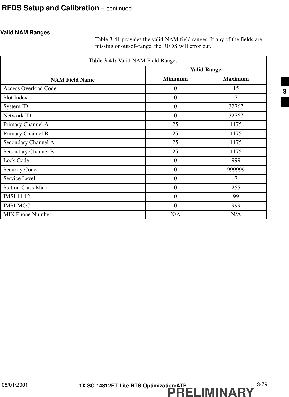
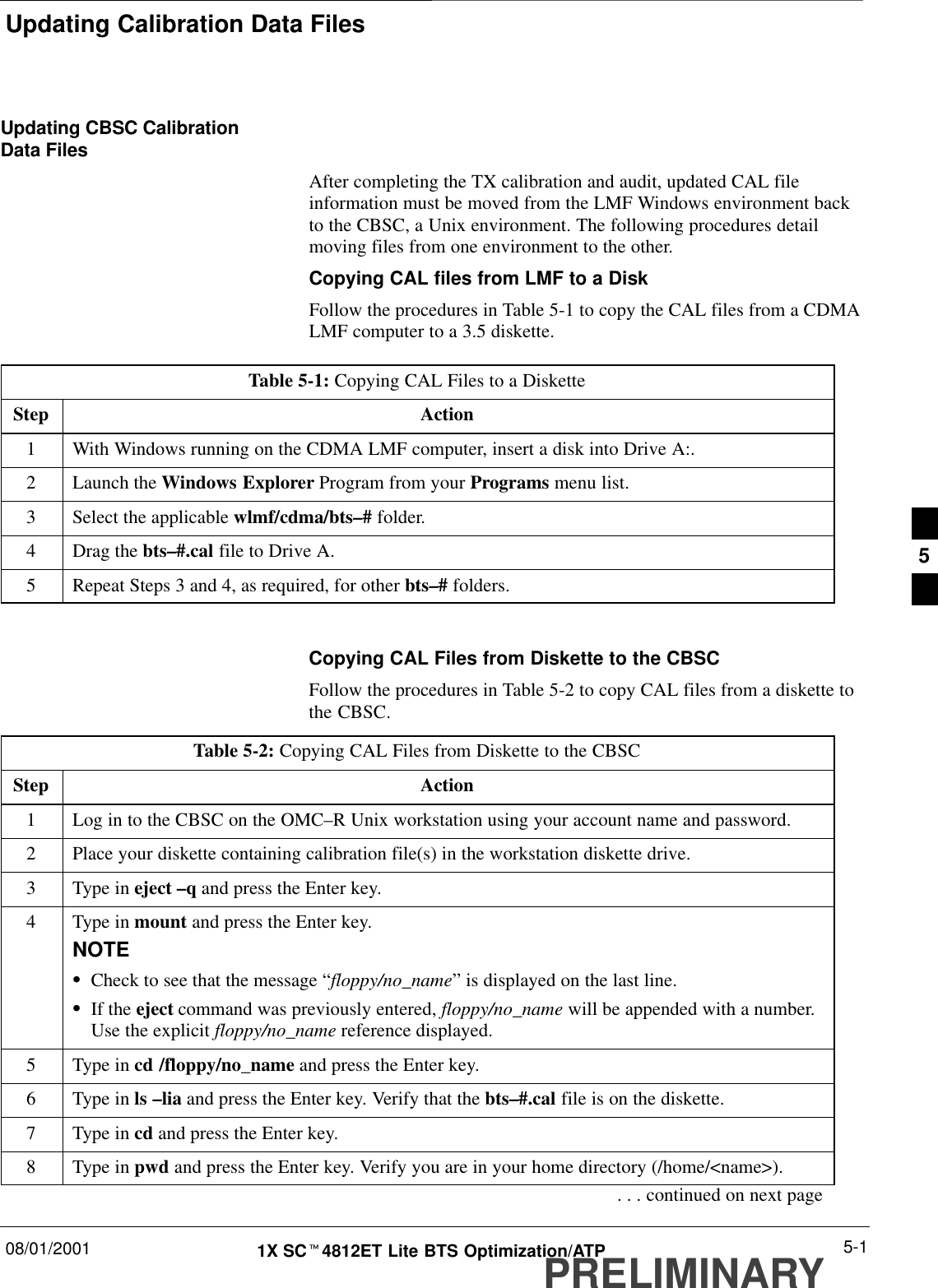
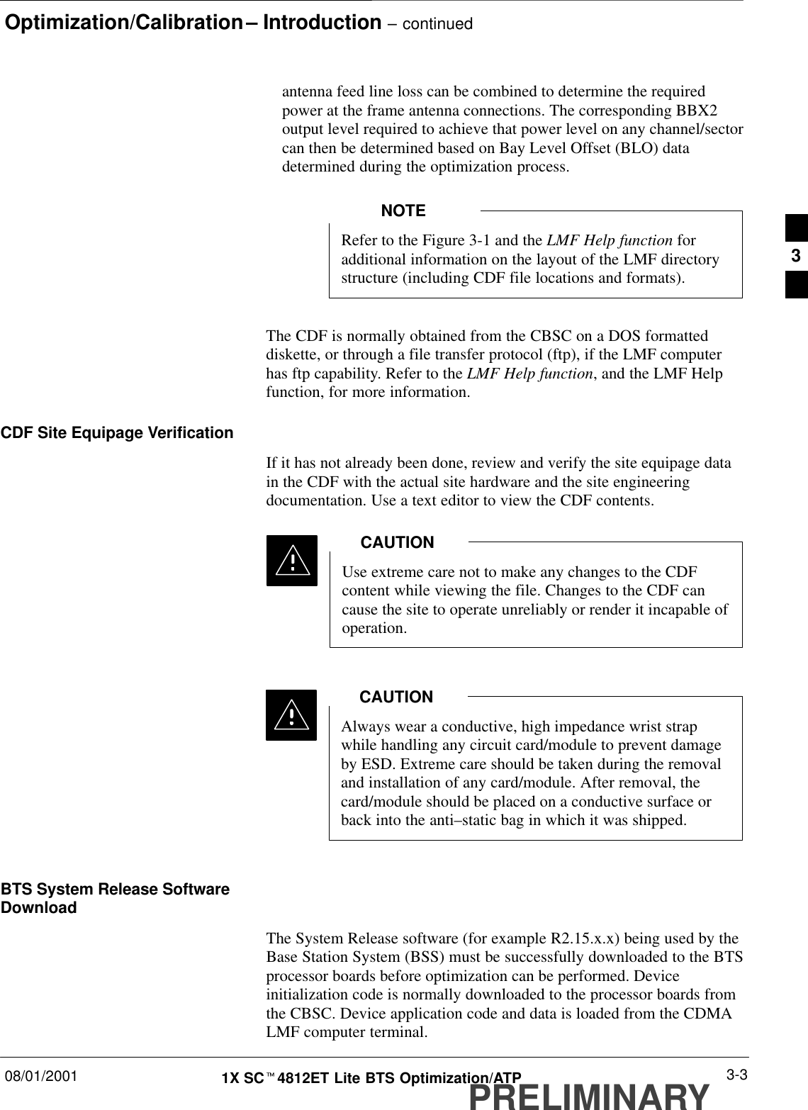
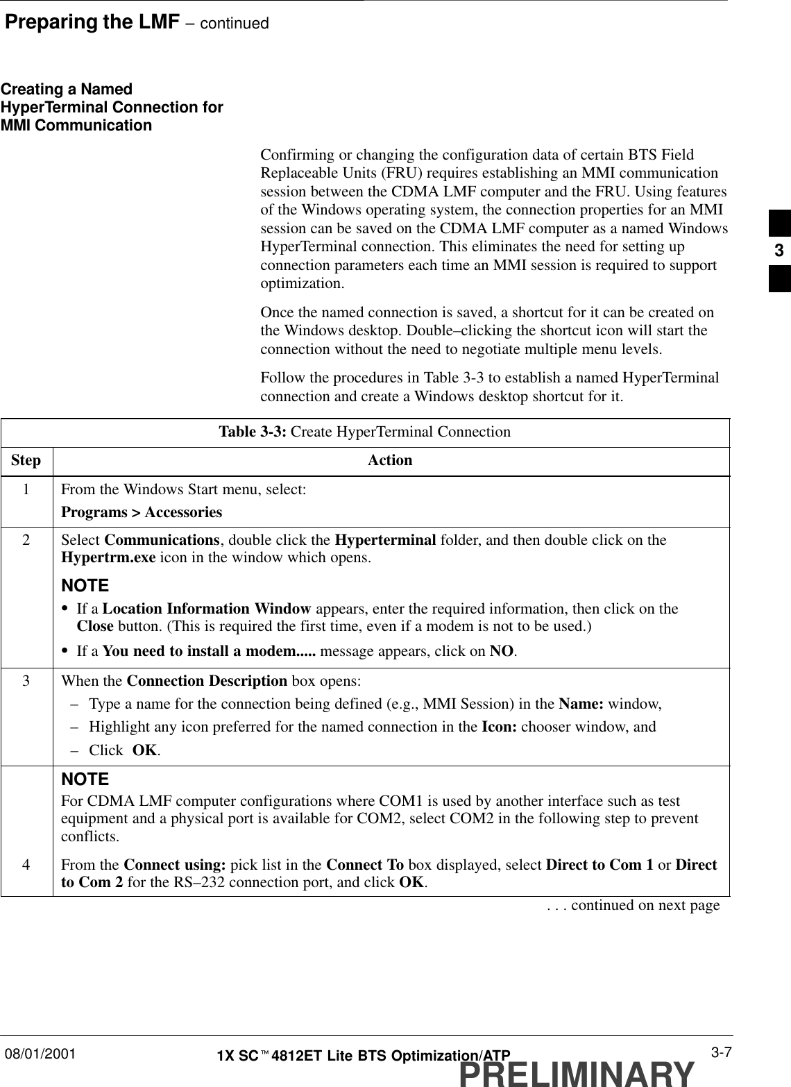
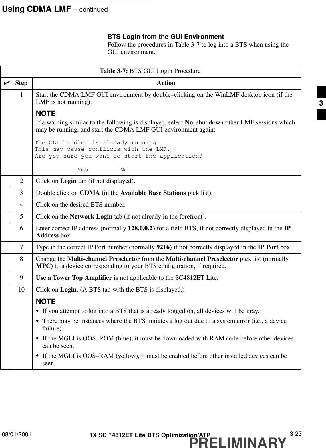
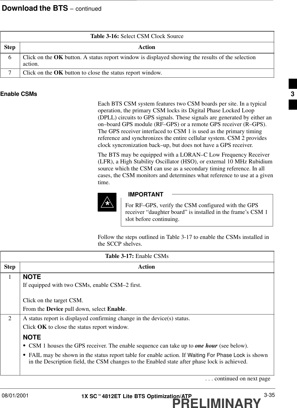
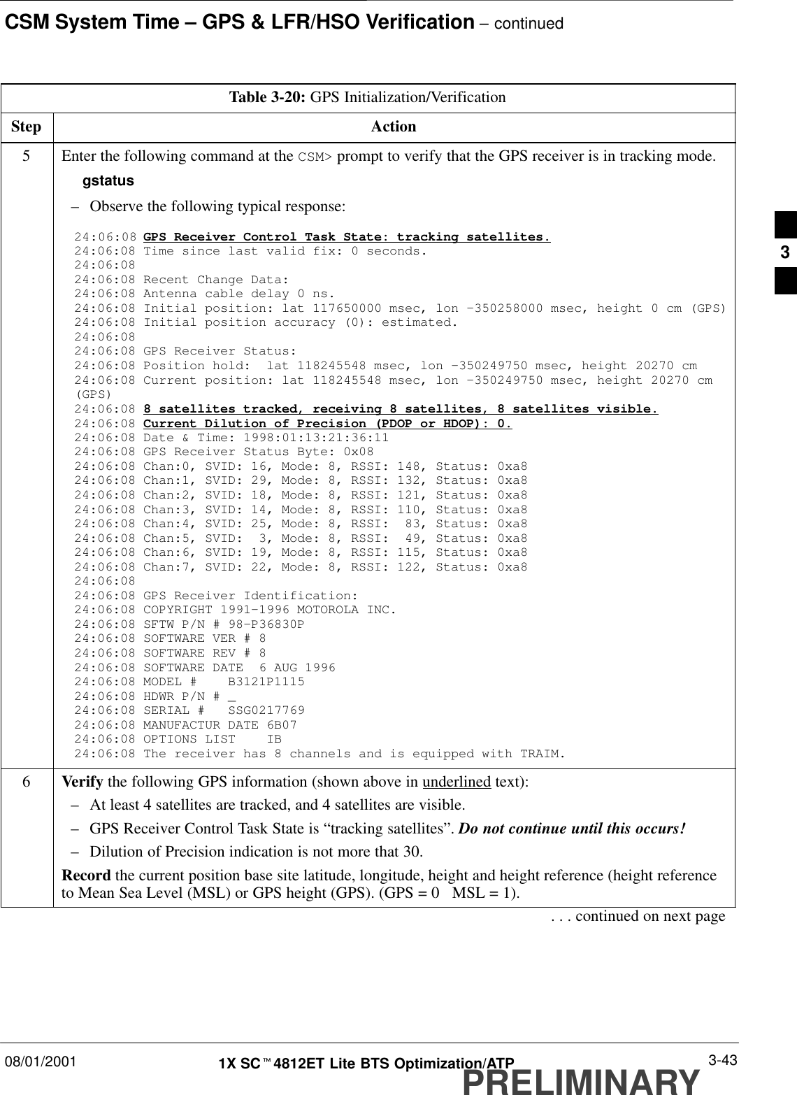
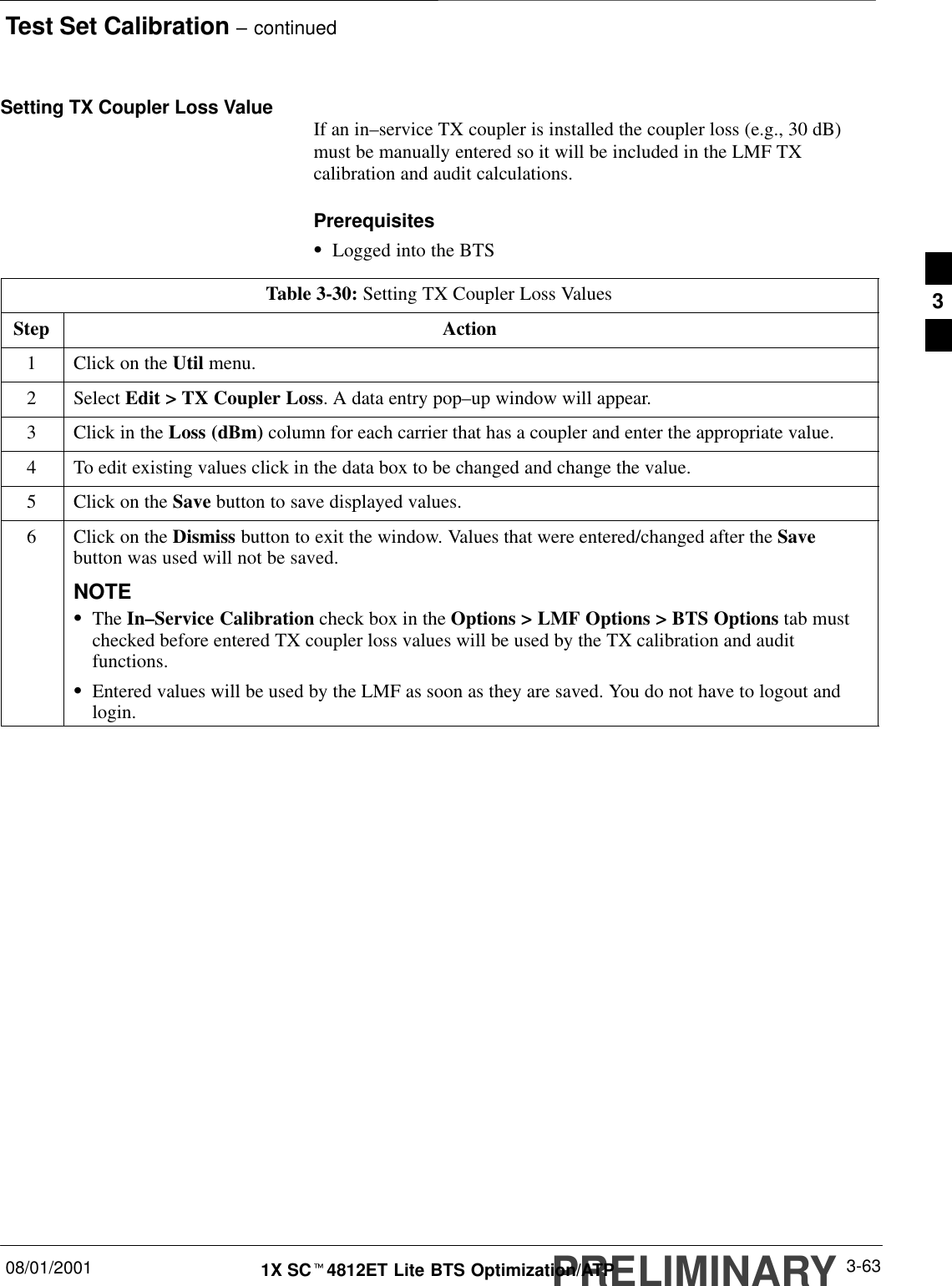
![Bay Level Offset Calibration – continuedPRELIMINARY1X SCt4812ET Lite BTS Optimization/ATP 08/01/20013-68(2500 corresponds to –125 dBm and 27500 corresponds to +125dBm).SThe 10 calibration points for each slot/branch combination must bestored in order of increasing frequency. If less than 10 points(frequencies) are calibrated, the BLO data for the highest frequencycalibrated is written into the remainder of the 10 points for thatslot/branch.Example:C[1]=384 (odd cal entry)C[2]=19102 (even cal entry)C[3]=777 (odd cal entry)C[4]=19086 (even cal entry)C[19]=777 (odd cal entry)C[20]=19086 (even cal entry)...= 1 “calibration point”In the example above, BLO was measured at only two frequencies(channels 384 and 777) for SCCP slot BBX–1 transmit (Table 3-32).The BLO data for the highest frequency measured (777) will bewritten to the remaining eight transmit calibration points (defined byentries C[5] through C[20]) for BBX2–1.SWhen BLO data is downloaded to the BBXs, the data is downloadedto the devices in the order it is stored in the CAL file. TxCal data(C[1] – C[60]) is sent first. BBX2 slot 1’s 10 calibration points (C[1]– C[20]) are sent initially, followed by BBX2 slot 2’s 10 calibrationpoints (C[21] – C[40]), and so on. The RxCal data is sent next,followed by the RxDCal data.STemperature compensation data (TempLevelCal) is also stored in theCAL file for each slot Block.Test Equipment Setup:RF Path CalibrationFollow the steps outlined in Table 3-33 and refer as needed toFigure 3-15 or Figure 3-16 to set up test equipment.Table 3-33: Set Up Test Equipment (RF Path Calibration)Step Action1If it has not already been done, refer to the procedure in Table 3-6 to interface the CDMA LMFcomputer terminal to the frame LAN A connector.2If it has not already been done, refer to Table 3-7 to start a GUI LMF session.3If required, calibrate the test equipment per the procedure in Table 3-25.3](https://usermanual.wiki/Nokia-Solutions-and-Networks/T5BR1.IHET5BR1-User-Manual-Part-2-of-3/User-Guide-170603-Page-66.png)