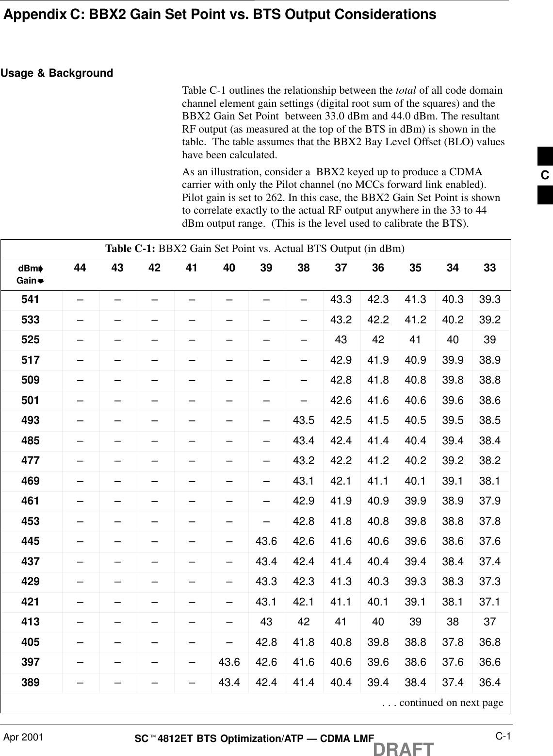
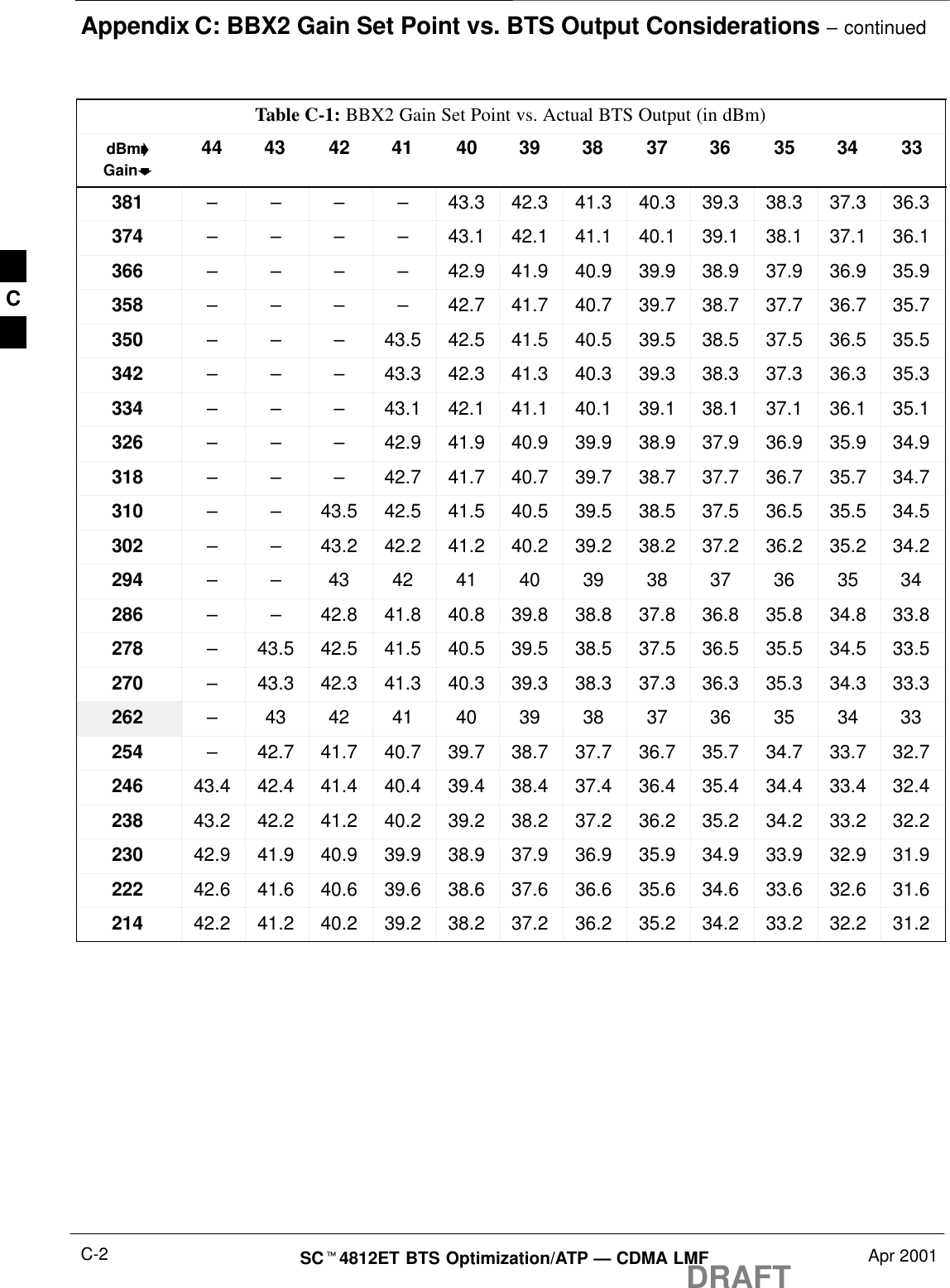
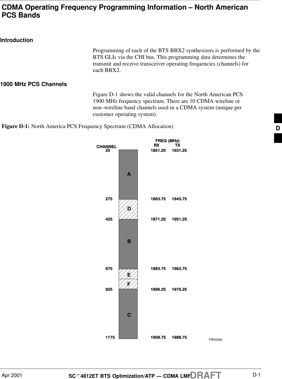
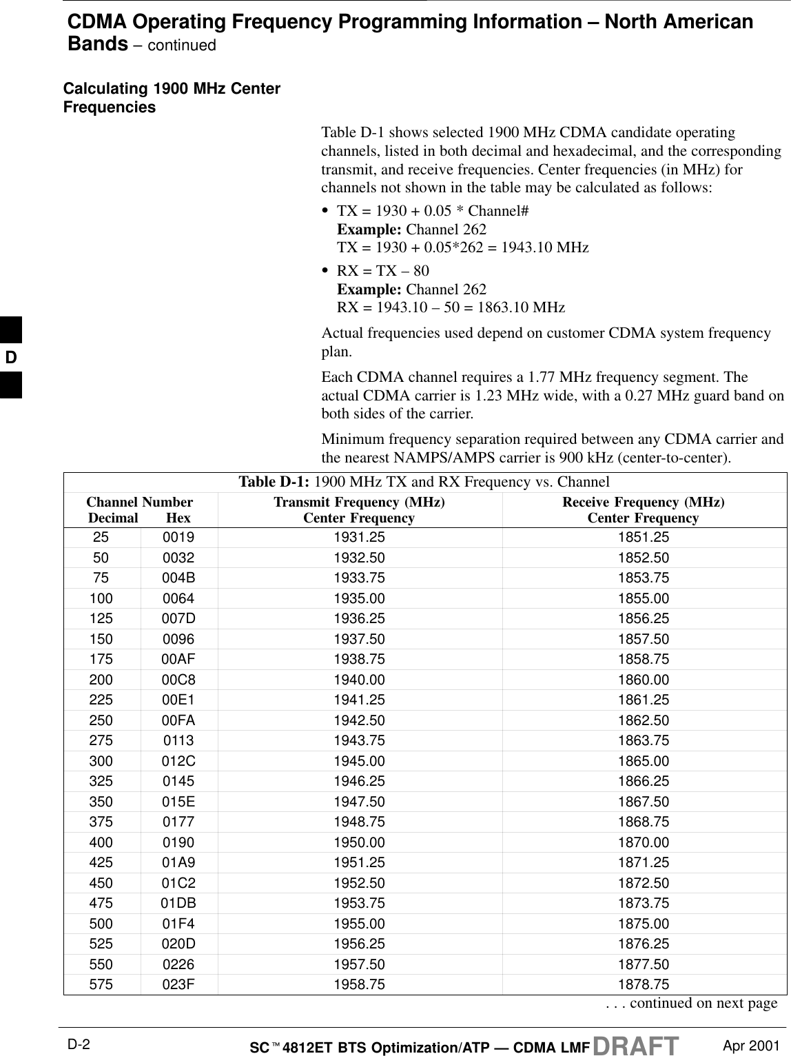
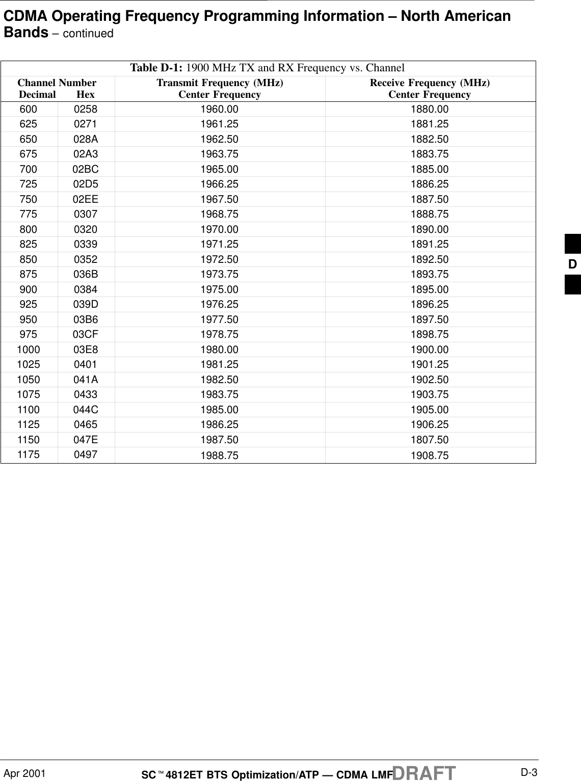
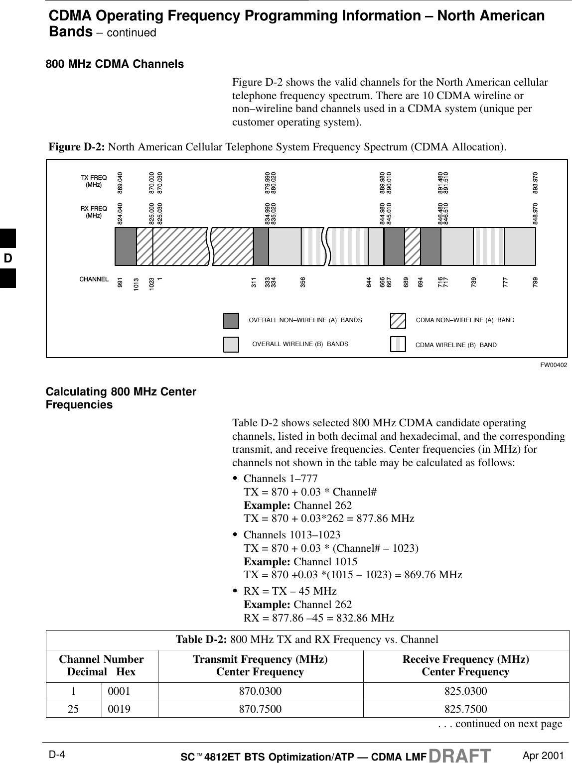
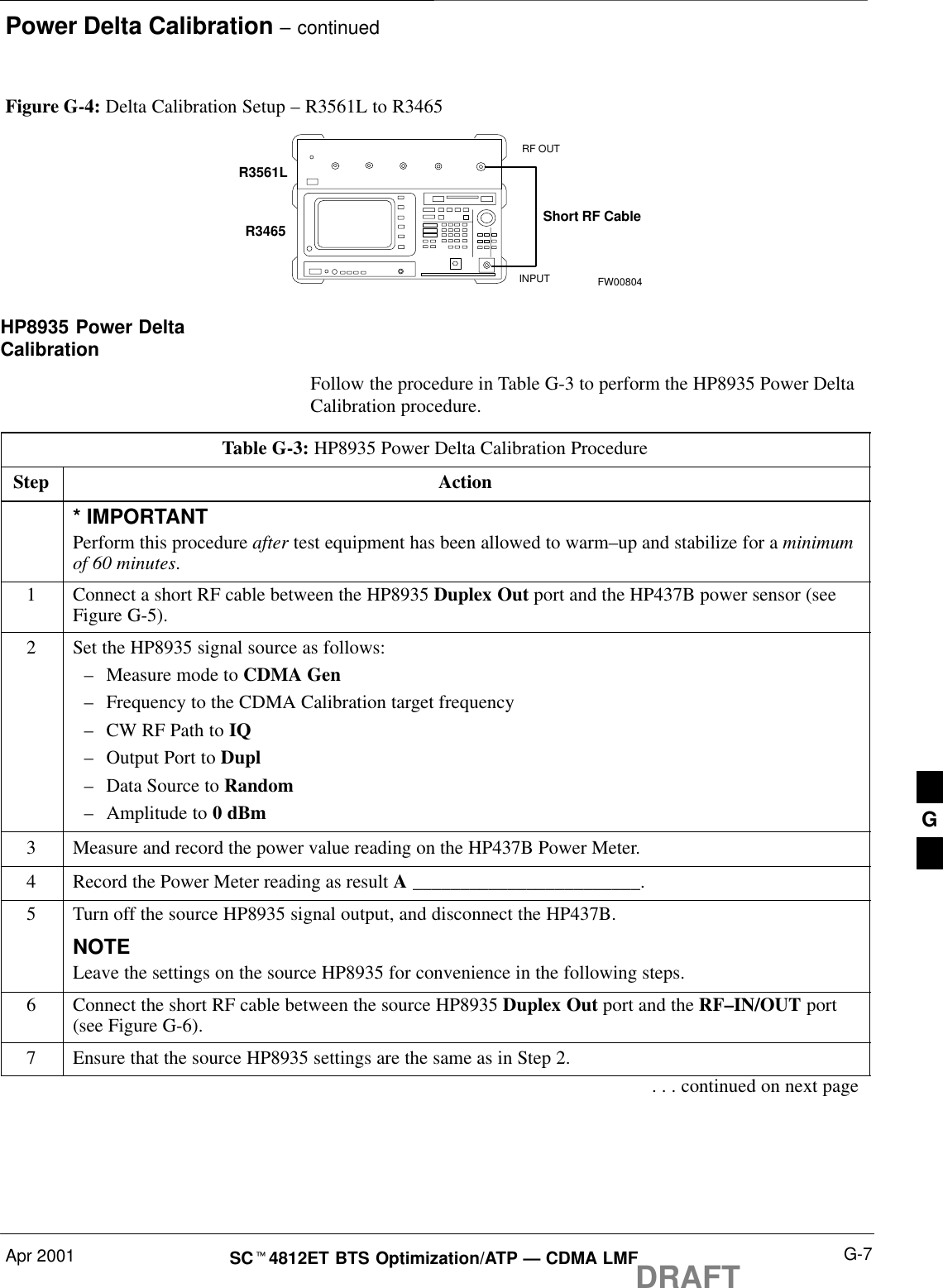
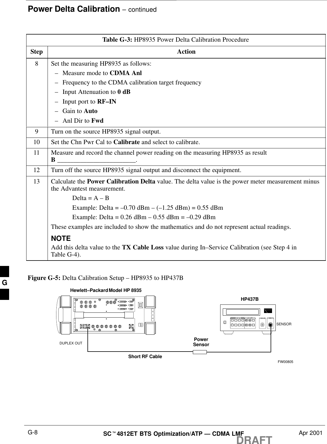
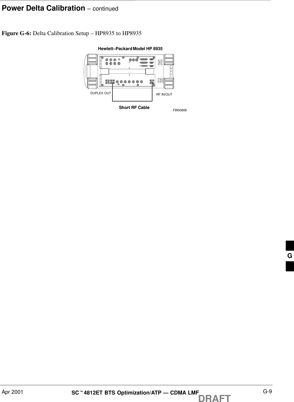
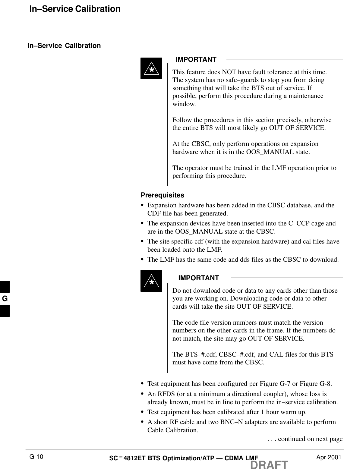
Nokia Solutions and Networks T5BQ1 Part 22 Cellular CDMA base station User Manual IHET5BQ1 Part 3 of 3

Nokia Solutions and Networks Part 22 Cellular CDMA base station IHET5BQ1 Part 3 of 3

IHET5BQ1 User Manual Part 3 of 3
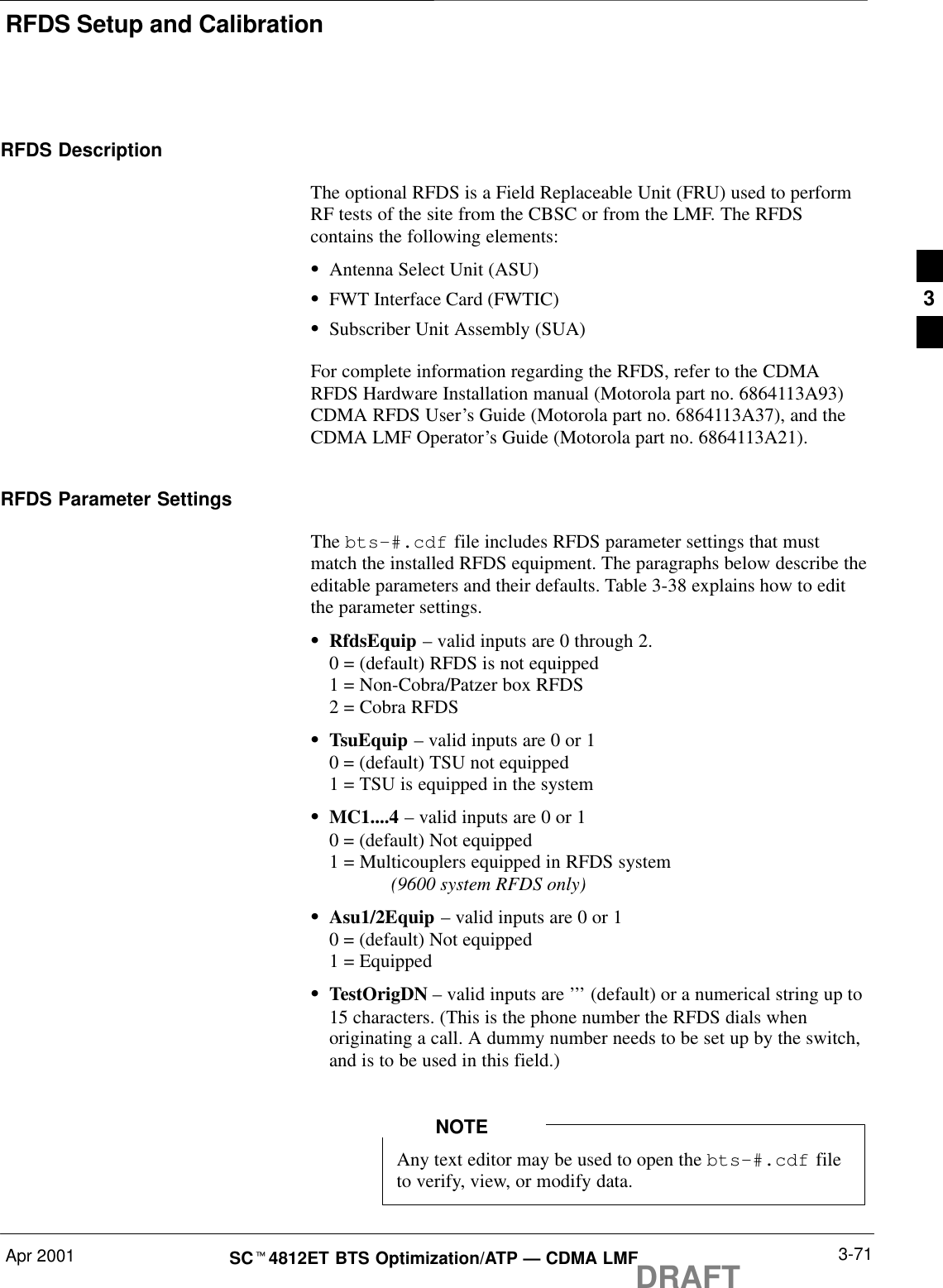
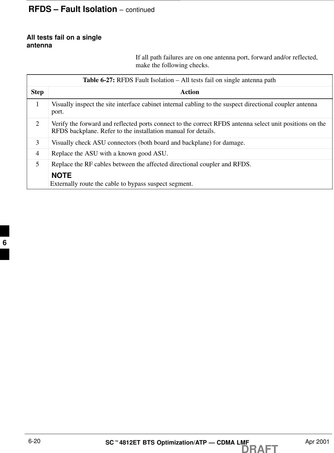
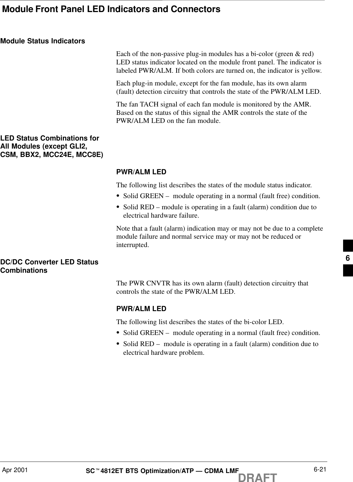
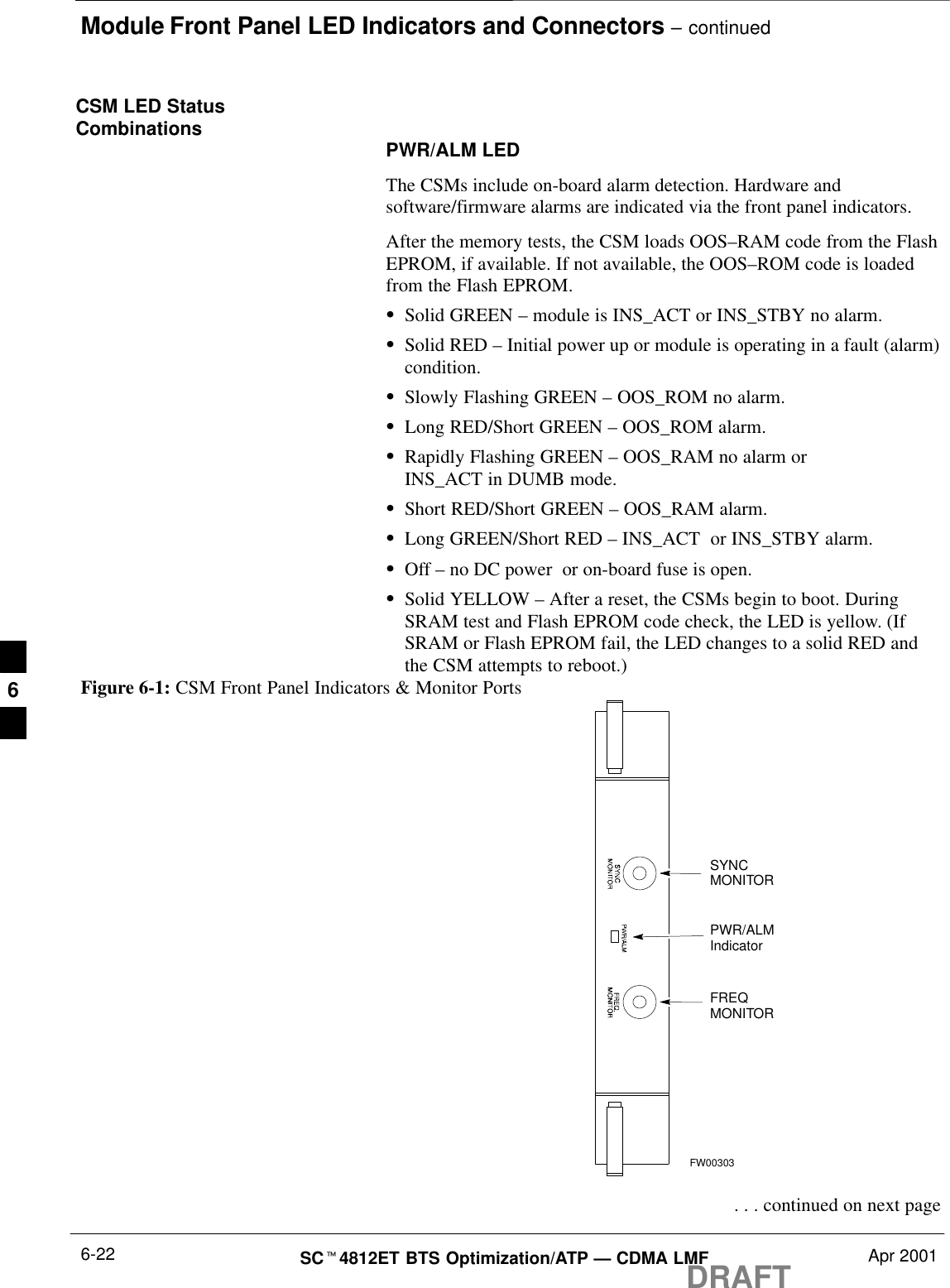
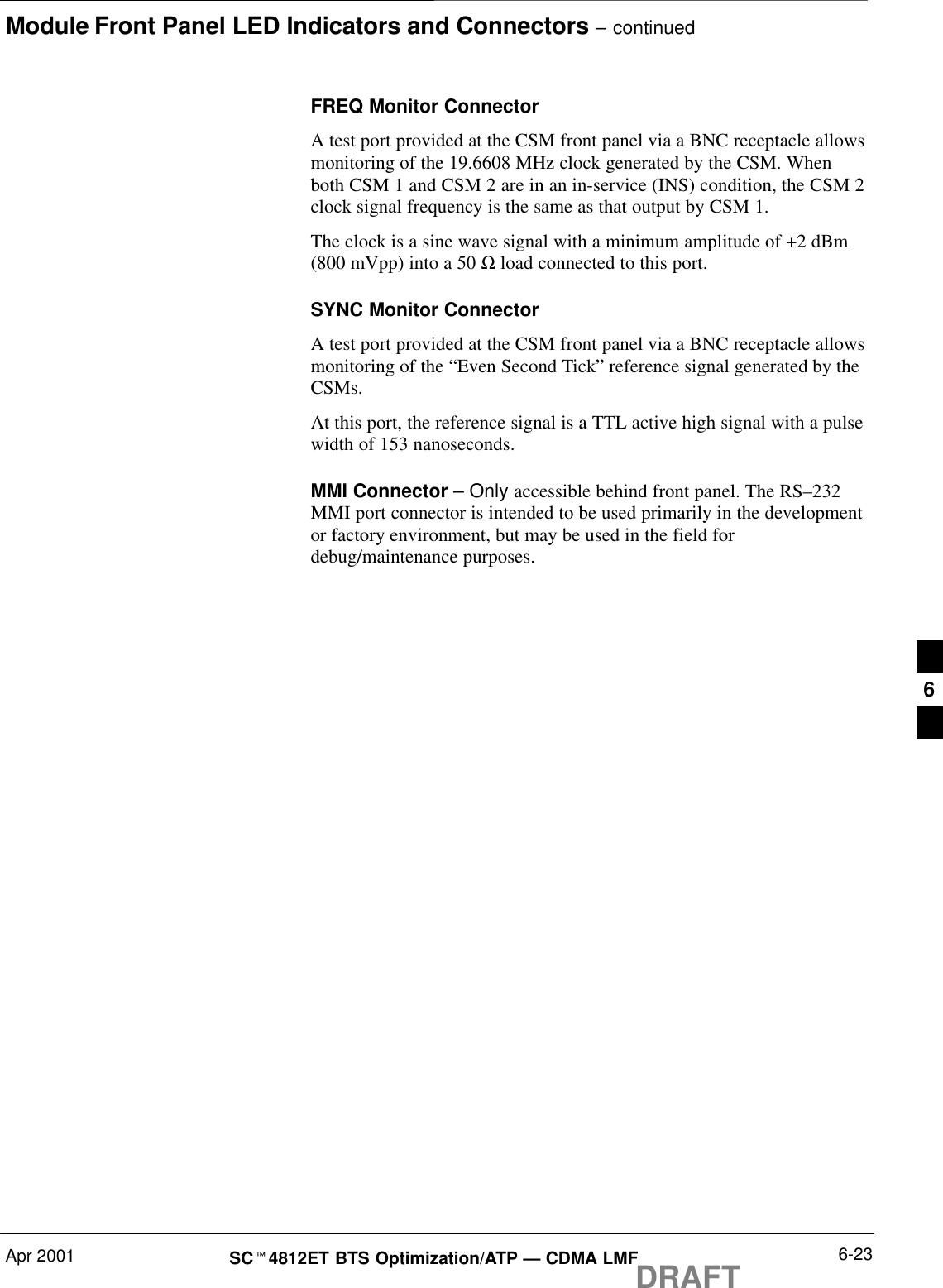
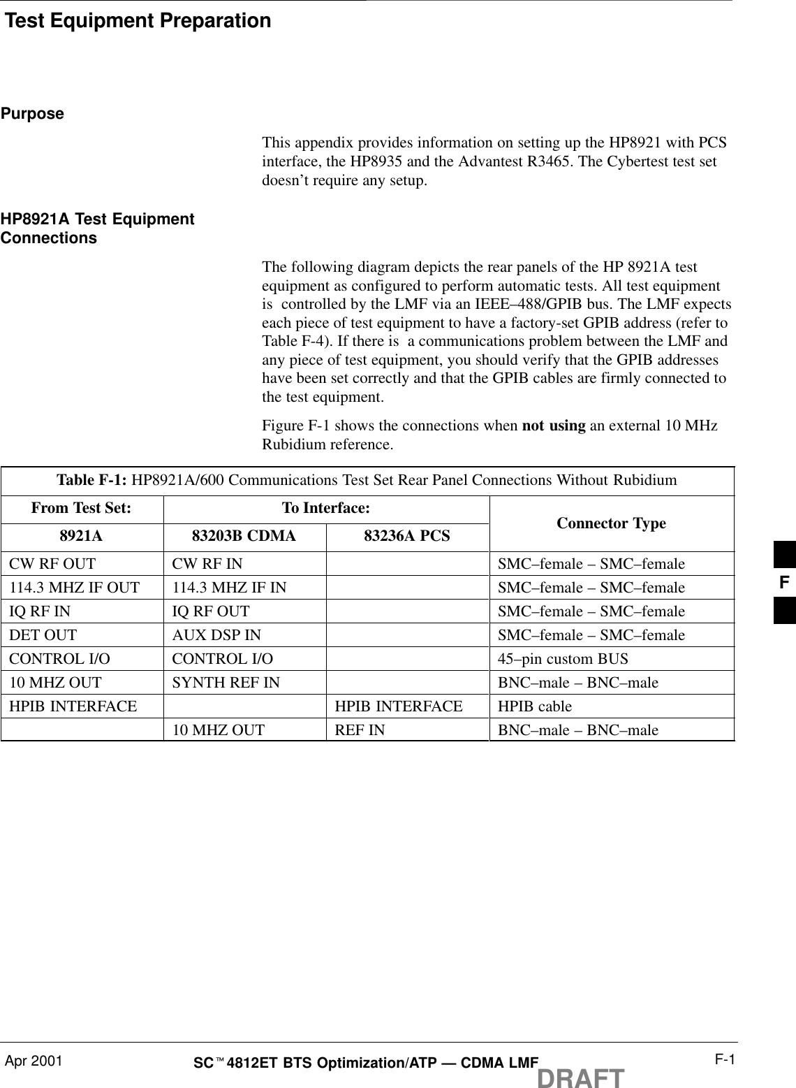
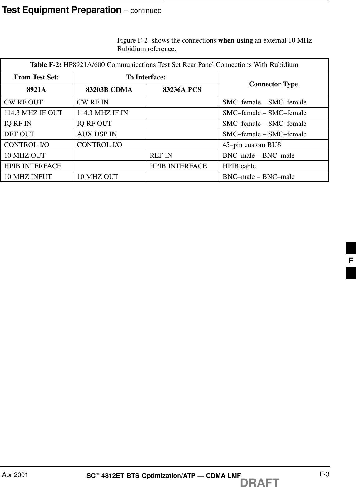
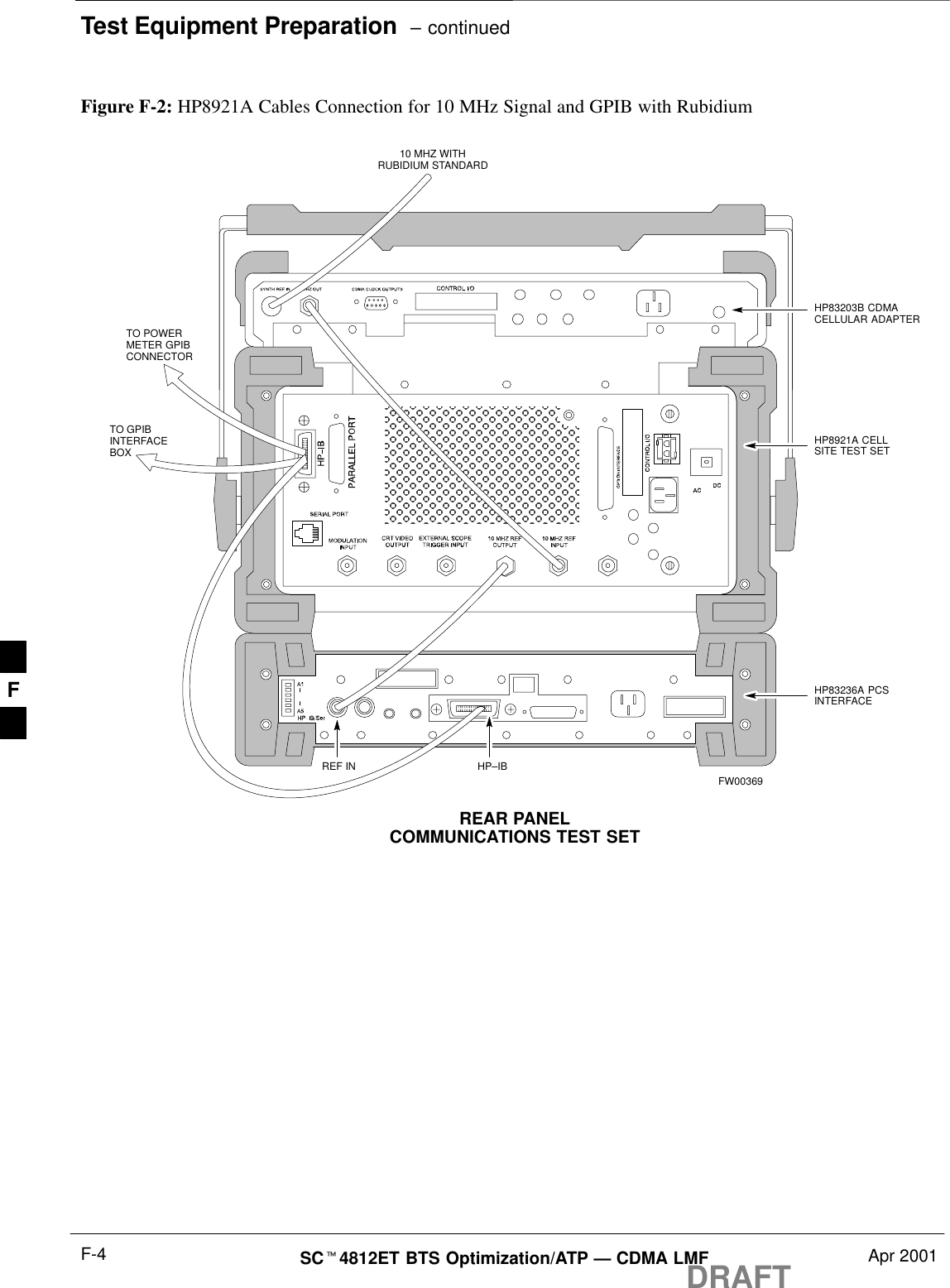
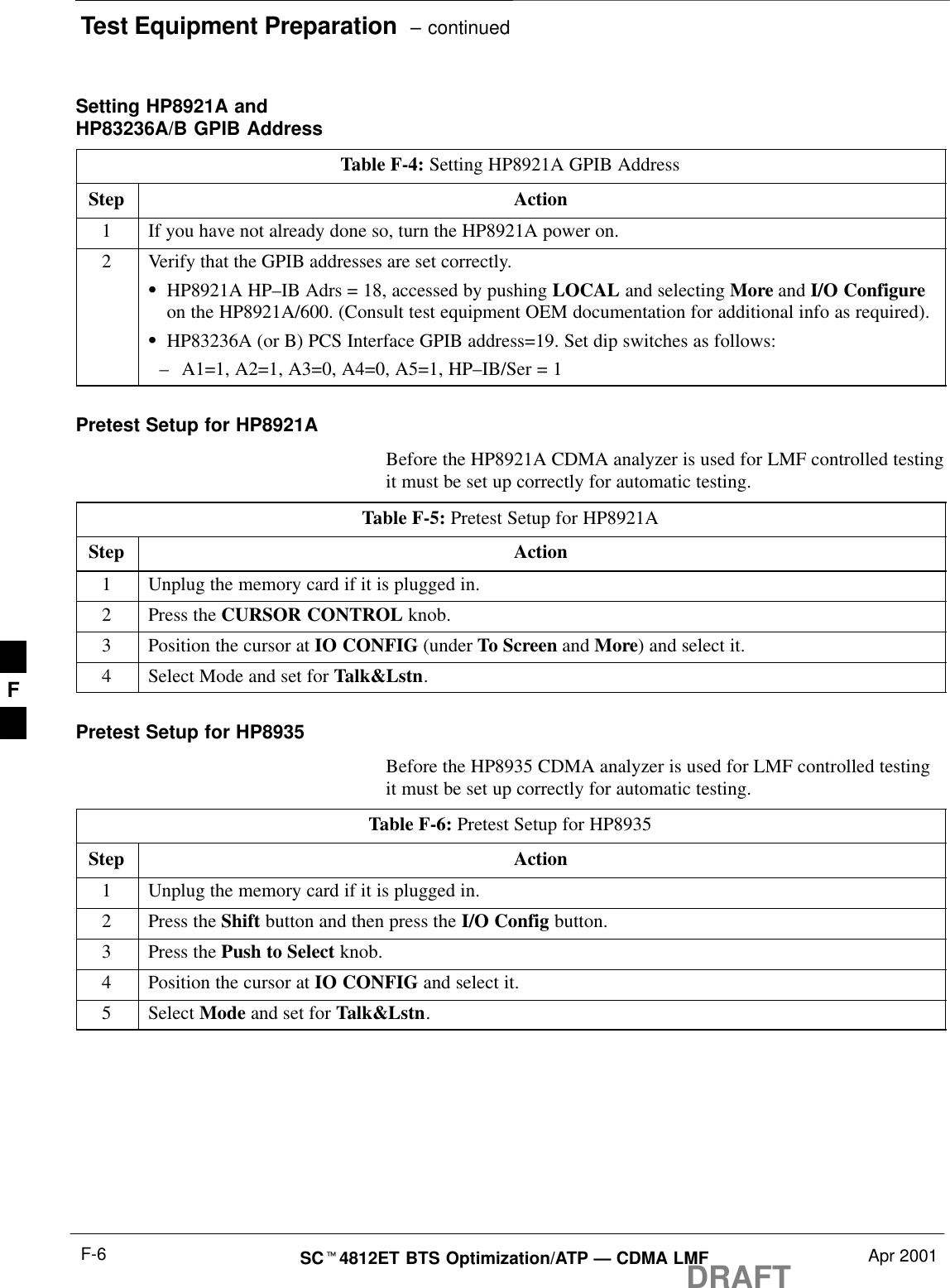
RFDS Setup and CalibrationApr 2001 3-71SCt4812ET BTS Optimization/ATP — CDMA LMFDRAFTRFDS DescriptionThe optional RFDS is a Field Replaceable Unit (FRU) used to performRF tests of the site from the CBSC or from the LMF. The RFDScontains the following elements:SAntenna Select Unit (ASU)SFWT Interface Card (FWTIC)SSubscriber Unit Assembly (SUA)For complete information regarding the RFDS, refer to the CDMARFDS Hardware Installation manual (Motorola part no. 6864113A93)CDMA RFDS User’s Guide (Motorola part no. 6864113A37), and theCDMA LMF Operator’s Guide (Motorola part no. 6864113A21).RFDS Parameter SettingsThe bts-#.cdf file includes RFDS parameter settings that mustmatch the installed RFDS equipment. The paragraphs below describe theeditable parameters and their defaults. Table 3-38 explains how to editthe parameter settings.SRfdsEquip – valid inputs are 0 through 2.0 = (default) RFDS is not equipped1 = Non-Cobra/Patzer box RFDS2 = Cobra RFDSSTsuEquip – valid inputs are 0 or 10 = (default) TSU not equipped1 = TSU is equipped in the systemSMC1....4 – valid inputs are 0 or 10 = (default) Not equipped1 = Multicouplers equipped in RFDS system (9600 system RFDS only)SAsu1/2Equip – valid inputs are 0 or 10 = (default) Not equipped1 = EquippedSTestOrigDN – valid inputs are ’’’ (default) or a numerical string up to15 characters. (This is the phone number the RFDS dials whenoriginating a call. A dummy number needs to be set up by the switch,and is to be used in this field.)Any text editor may be used to open the bts–#.cdf fileto verify, view, or modify data.NOTE3
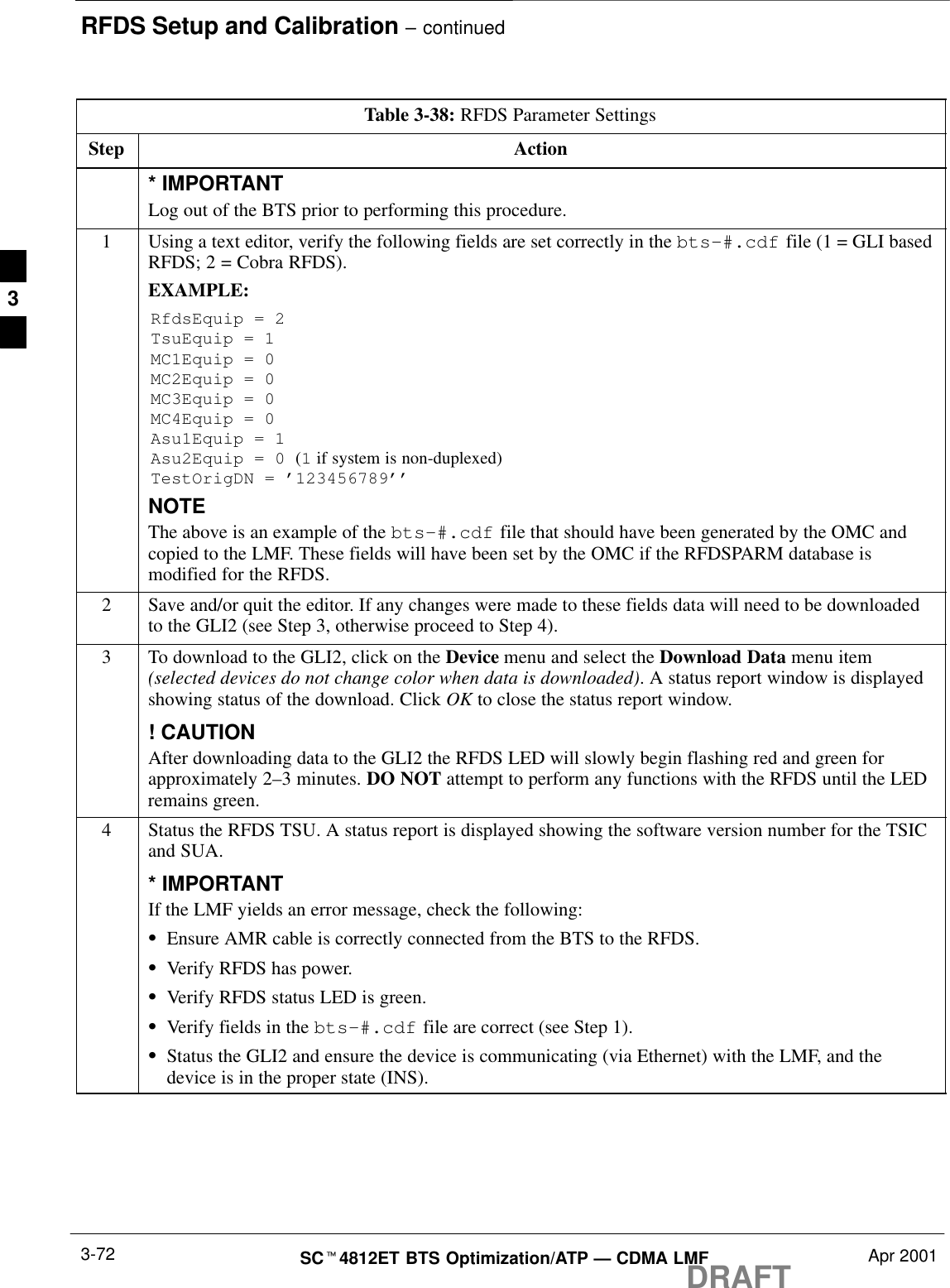
RFDS Setup and Calibration – continuedDRAFTSCt4812ET BTS Optimization/ATP — CDMA LMF Apr 20013-72Table 3-38: RFDS Parameter SettingsStep Action* IMPORTANTLog out of the BTS prior to performing this procedure.1Using a text editor, verify the following fields are set correctly in the bts–#.cdf file (1 = GLI basedRFDS; 2 = Cobra RFDS).EXAMPLE:RfdsEquip = 2TsuEquip = 1MC1Equip = 0MC2Equip = 0MC3Equip = 0MC4Equip = 0Asu1Equip = 1Asu2Equip = 0 (1 if system is non-duplexed)TestOrigDN = ’123456789’’NOTEThe above is an example of the bts-#.cdf file that should have been generated by the OMC andcopied to the LMF. These fields will have been set by the OMC if the RFDSPARM database ismodified for the RFDS.2Save and/or quit the editor. If any changes were made to these fields data will need to be downloadedto the GLI2 (see Step 3, otherwise proceed to Step 4).3To download to the GLI2, click on the Device menu and select the Download Data menu item(selected devices do not change color when data is downloaded). A status report window is displayedshowing status of the download. Click OK to close the status report window.! CAUTIONAfter downloading data to the GLI2 the RFDS LED will slowly begin flashing red and green forapproximately 2–3 minutes. DO NOT attempt to perform any functions with the RFDS until the LEDremains green.4Status the RFDS TSU. A status report is displayed showing the software version number for the TSICand SUA.* IMPORTANTIf the LMF yields an error message, check the following:SEnsure AMR cable is correctly connected from the BTS to the RFDS.SVerify RFDS has power.SVerify RFDS status LED is green.SVerify fields in the bts-#.cdf file are correct (see Step 1).SStatus the GLI2 and ensure the device is communicating (via Ethernet) with the LMF, and thedevice is in the proper state (INS).3
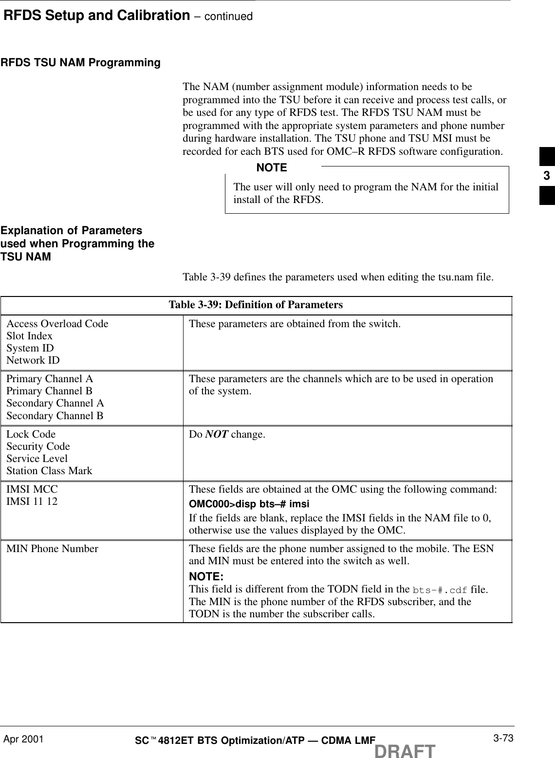
RFDS Setup and Calibration – continuedApr 2001 3-73SCt4812ET BTS Optimization/ATP — CDMA LMFDRAFTRFDS TSU NAM ProgrammingThe NAM (number assignment module) information needs to beprogrammed into the TSU before it can receive and process test calls, orbe used for any type of RFDS test. The RFDS TSU NAM must beprogrammed with the appropriate system parameters and phone numberduring hardware installation. The TSU phone and TSU MSI must berecorded for each BTS used for OMC–R RFDS software configuration.The user will only need to program the NAM for the initialinstall of the RFDS.NOTEExplanation of Parametersused when Programming theTSU NAMTable 3-39 defines the parameters used when editing the tsu.nam file.Table 3-39: Definition of ParametersAccess Overload CodeSlot IndexSystem IDNetwork IDThese parameters are obtained from the switch.Primary Channel APrimary Channel BSecondary Channel ASecondary Channel BThese parameters are the channels which are to be used in operationof the system.Lock CodeSecurity CodeService LevelStation Class MarkDo NOT change.IMSI MCCIMSI 11 12 These fields are obtained at the OMC using the following command:OMC000>disp bts–# imsiIf the fields are blank, replace the IMSI fields in the NAM file to 0,otherwise use the values displayed by the OMC.MIN Phone Number These fields are the phone number assigned to the mobile. The ESNand MIN must be entered into the switch as well.NOTE:This field is different from the TODN field in the bts-#.cdf file.The MIN is the phone number of the RFDS subscriber, and theTODN is the number the subscriber calls.3
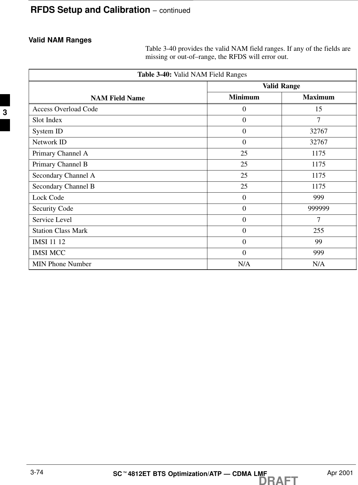
RFDS Setup and Calibration – continuedDRAFTSCt4812ET BTS Optimization/ATP — CDMA LMF Apr 20013-74Valid NAM Ranges Table 3-40 provides the valid NAM field ranges. If any of the fields aremissing or out-of–range, the RFDS will error out.Table 3-40: Valid NAM Field RangesValid RangeNAM Field Name Minimum MaximumAccess Overload Code 0 15Slot Index 0 7System ID 0 32767Network ID 0 32767Primary Channel A 25 1175Primary Channel B 25 1175Secondary Channel A 25 1175Secondary Channel B 25 1175Lock Code 0 999Security Code 0 999999Service Level 0 7Station Class Mark 0 255IMSI 11 12 0 99IMSI MCC 0 999MIN Phone Number N/A N/A3
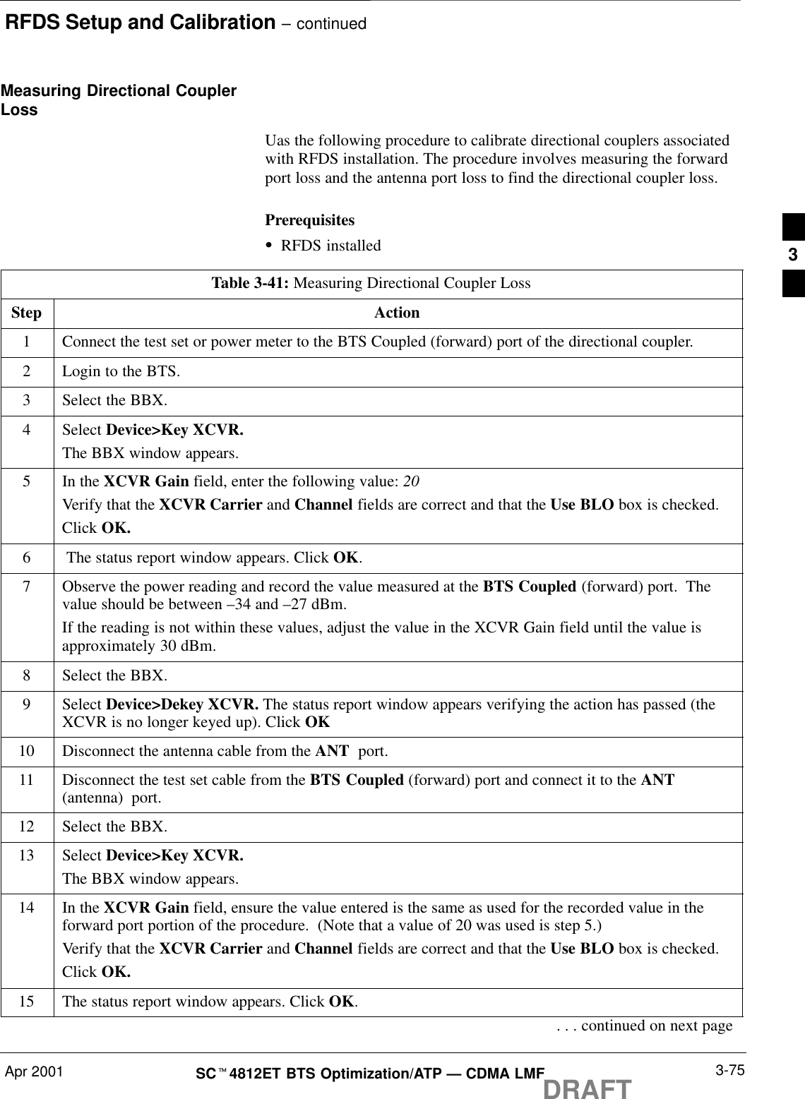
RFDS Setup and Calibration – continuedApr 2001 3-75SCt4812ET BTS Optimization/ATP — CDMA LMFDRAFTMeasuring Directional CouplerLossUas the following procedure to calibrate directional couplers associatedwith RFDS installation. The procedure involves measuring the forwardport loss and the antenna port loss to find the directional coupler loss.PrerequisitesSRFDS installedTable 3-41: Measuring Directional Coupler LossStep Action1Connect the test set or power meter to the BTS Coupled (forward) port of the directional coupler.2Login to the BTS.3Select the BBX.4 Select Device>Key XCVR.The BBX window appears.5In the XCVR Gain field, enter the following value: 20Verify that the XCVR Carrier and Channel fields are correct and that the Use BLO box is checked.Click OK.6 The status report window appears. Click OK.7Observe the power reading and record the value measured at the BTS Coupled (forward) port.  Thevalue should be between –34 and –27 dBm.If the reading is not within these values, adjust the value in the XCVR Gain field until the value isapproximately 30 dBm.8Select the BBX.9 Select Device>Dekey XCVR. The status report window appears verifying the action has passed (theXCVR is no longer keyed up). Click OK10 Disconnect the antenna cable from the ANT  port.11 Disconnect the test set cable from the BTS Coupled (forward) port and connect it to the ANT(antenna)  port.12 Select the BBX.13 Select Device>Key XCVR.The BBX window appears.14 In the XCVR Gain field, ensure the value entered is the same as used for the recorded value in theforward port portion of the procedure.  (Note that a value of 20 was used is step 5.)Verify that the XCVR Carrier and Channel fields are correct and that the Use BLO box is checked.Click OK.15 The status report window appears. Click OK.. . . continued on next page3
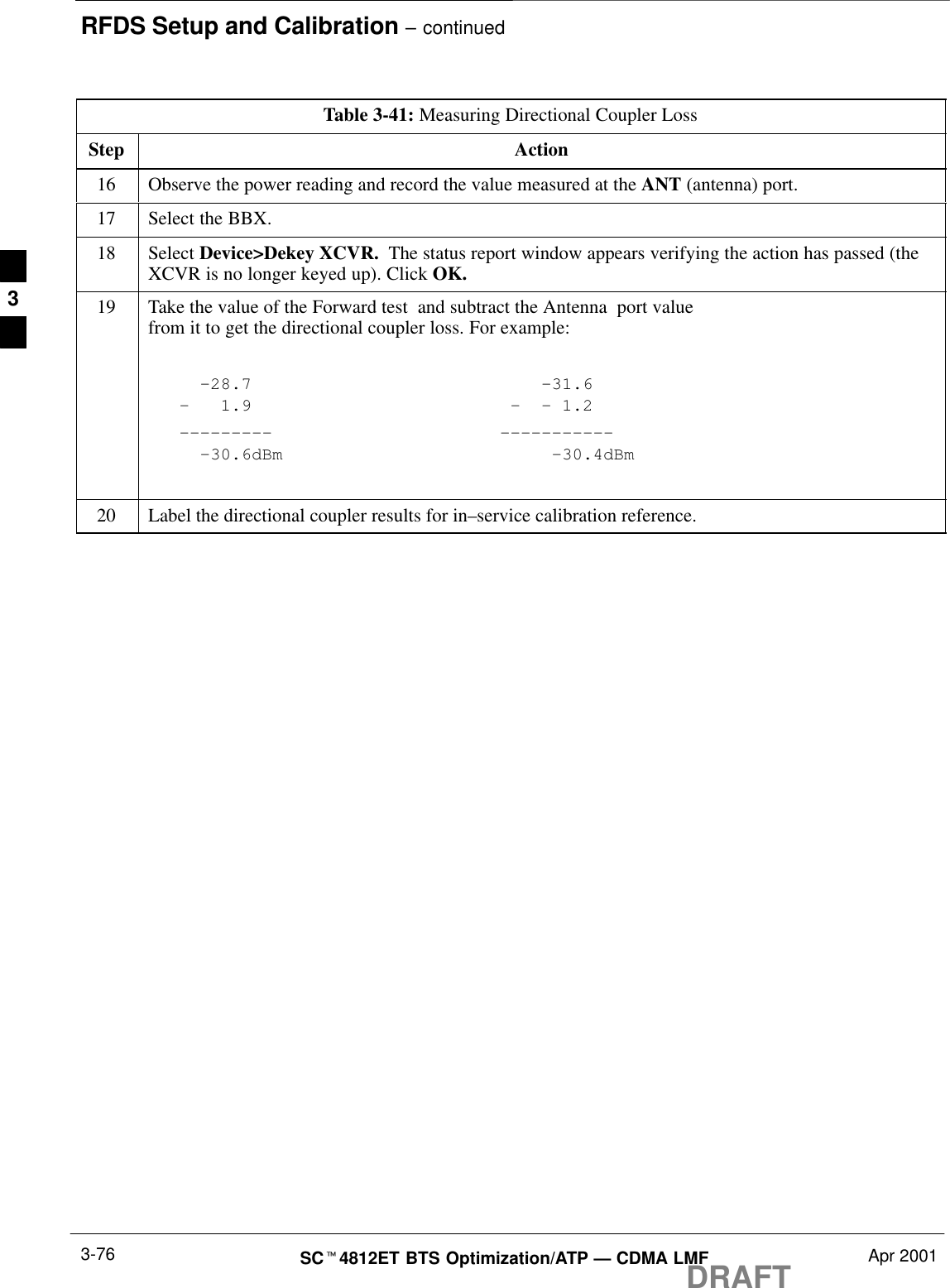
RFDS Setup and Calibration – continuedDRAFTSCt4812ET BTS Optimization/ATP — CDMA LMF Apr 20013-76Table 3-41: Measuring Directional Coupler LossStep Action16 Observe the power reading and record the value measured at the ANT (antenna) port.17 Select the BBX.18 Select Device>Dekey XCVR.  The status report window appears verifying the action has passed (theXCVR is no longer keyed up). Click OK.19 Take the value of the Forward test  and subtract the Antenna  port valuefrom it to get the directional coupler loss. For example:     –28.7                            –31.6               –   1.9                         –  – 1.2   –––––––––                      –––––––––––     –30.6dBm                          –30.4dBm20 Label the directional coupler results for in–service calibration reference. 3
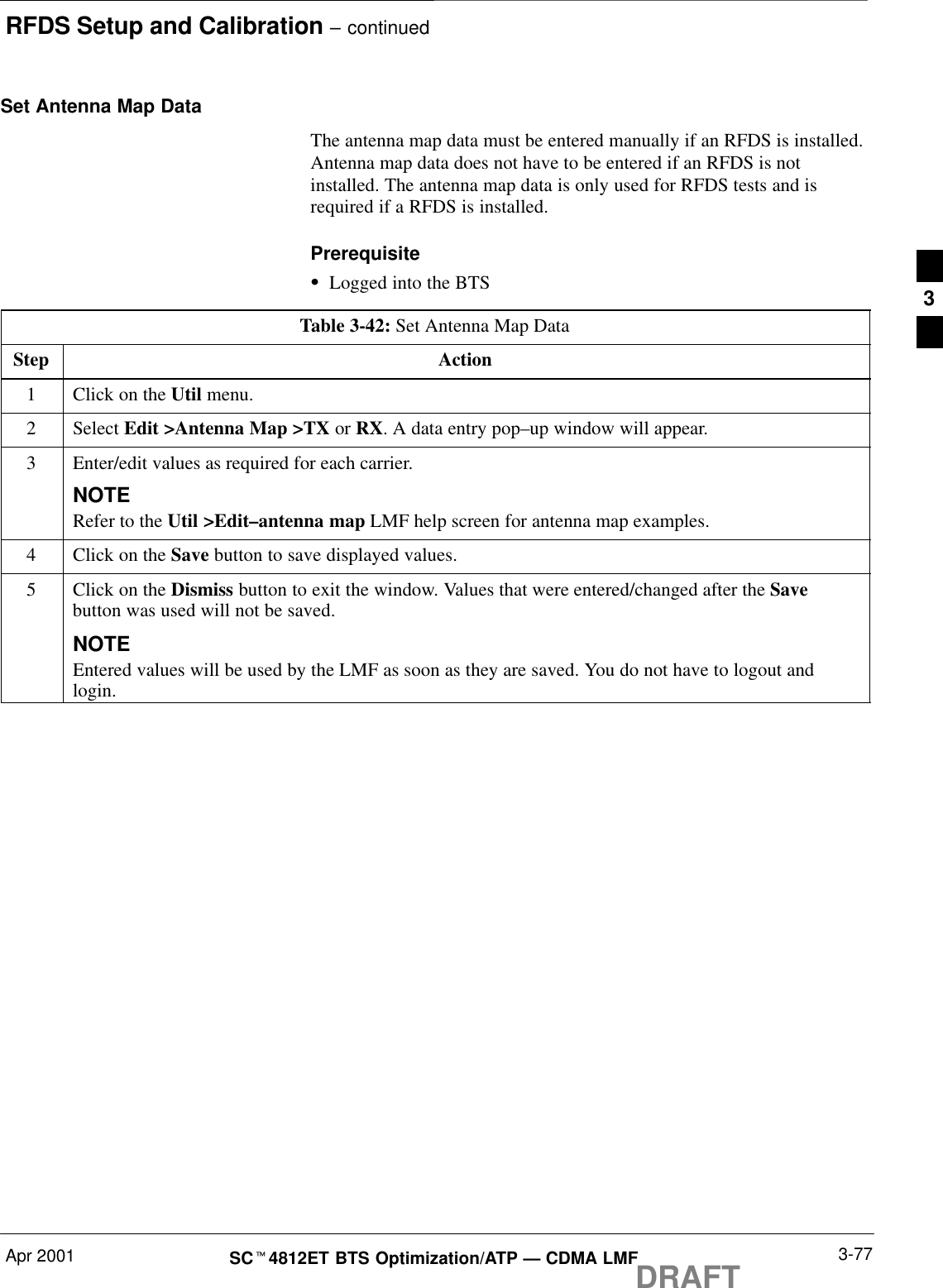
RFDS Setup and Calibration – continuedApr 2001 3-77SCt4812ET BTS Optimization/ATP — CDMA LMFDRAFTSet Antenna Map DataThe antenna map data must be entered manually if an RFDS is installed.Antenna map data does not have to be entered if an RFDS is notinstalled. The antenna map data is only used for RFDS tests and isrequired if a RFDS is installed.PrerequisiteSLogged into the BTSTable 3-42: Set Antenna Map DataStep Action1Click on the Util menu.2 Select Edit >Antenna Map >TX or RX. A data entry pop–up window will appear.3Enter/edit values as required for each carrier.NOTERefer to the Util >Edit–antenna map LMF help screen for antenna map examples.4Click on the Save button to save displayed values.5Click on the Dismiss button to exit the window. Values that were entered/changed after the Savebutton was used will not be saved.NOTEEntered values will be used by the LMF as soon as they are saved. You do not have to logout andlogin.3
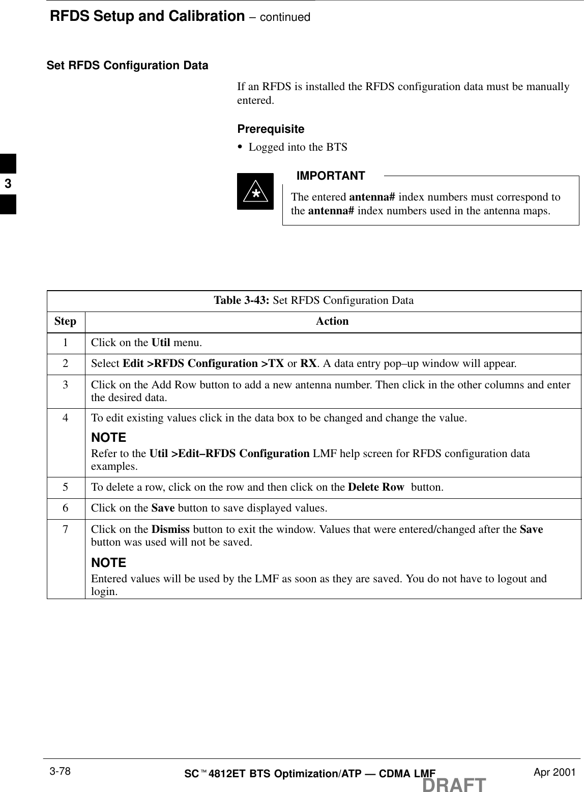
RFDS Setup and Calibration – continuedDRAFTSCt4812ET BTS Optimization/ATP — CDMA LMF Apr 20013-78Set RFDS Configuration DataIf an RFDS is installed the RFDS configuration data must be manuallyentered.PrerequisiteSLogged into the BTSThe entered antenna# index numbers must correspond tothe antenna# index numbers used in the antenna maps.IMPORTANT*Table 3-43: Set RFDS Configuration DataStep Action1Click on the Util menu.2 Select Edit >RFDS Configuration >TX or RX. A data entry pop–up window will appear.3Click on the Add Row button to add a new antenna number. Then click in the other columns and enterthe desired data.4To edit existing values click in the data box to be changed and change the value.NOTERefer to the Util >Edit–RFDS Configuration LMF help screen for RFDS configuration dataexamples.5To delete a row, click on the row and then click on the Delete Row  button.6Click on the Save button to save displayed values.7Click on the Dismiss button to exit the window. Values that were entered/changed after the Savebutton was used will not be saved.NOTEEntered values will be used by the LMF as soon as they are saved. You do not have to logout andlogin.3
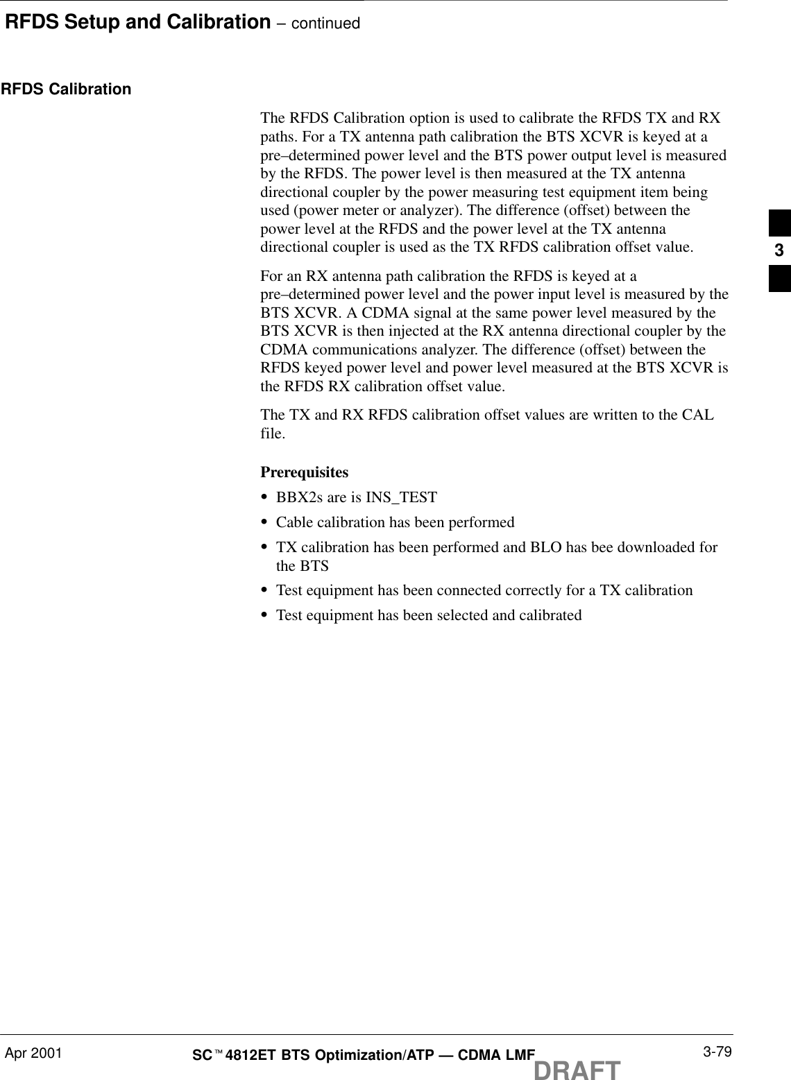
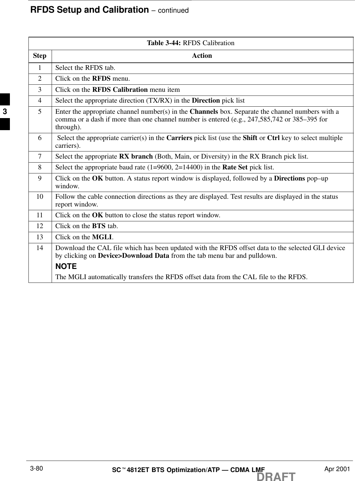
RFDS Setup and Calibration – continuedApr 2001 3-79SCt4812ET BTS Optimization/ATP — CDMA LMFDRAFTRFDS CalibrationThe RFDS Calibration option is used to calibrate the RFDS TX and RXpaths. For a TX antenna path calibration the BTS XCVR is keyed at apre–determined power level and the BTS power output level is measuredby the RFDS. The power level is then measured at the TX antennadirectional coupler by the power measuring test equipment item beingused (power meter or analyzer). The difference (offset) between thepower level at the RFDS and the power level at the TX antennadirectional coupler is used as the TX RFDS calibration offset value.For an RX antenna path calibration the RFDS is keyed at apre–determined power level and the power input level is measured by theBTS XCVR. A CDMA signal at the same power level measured by theBTS XCVR is then injected at the RX antenna directional coupler by theCDMA communications analyzer. The difference (offset) between theRFDS keyed power level and power level measured at the BTS XCVR isthe RFDS RX calibration offset value.The TX and RX RFDS calibration offset values are written to the CALfile.PrerequisitesSBBX2s are is INS_TESTSCable calibration has been performedSTX calibration has been performed and BLO has bee downloaded forthe BTSSTest equipment has been connected correctly for a TX calibrationSTest equipment has been selected and calibrated3
RFDS Setup and Calibration – continuedDRAFTSCt4812ET BTS Optimization/ATP — CDMA LMF Apr 20013-80Table 3-44: RFDS CalibrationStep Action1Select the RFDS tab.2Click on the RFDS menu.3Click on the RFDS Calibration menu item4Select the appropriate direction (TX/RX) in the Direction pick list5Enter the appropriate channel number(s) in the Channels box. Separate the channel numbers with acomma or a dash if more than one channel number is entered (e.g., 247,585,742 or 385–395 forthrough).6 Select the appropriate carrier(s) in the Carriers pick list (use the Shift or Ctrl key to select multiplecarriers).7Select the appropriate RX branch (Both, Main, or Diversity) in the RX Branch pick list.8Select the appropriate baud rate (1=9600, 2=14400) in the Rate Set pick list.9Click on the OK button. A status report window is displayed, followed by a Directions pop–upwindow.10 Follow the cable connection directions as they are displayed. Test results are displayed in the statusreport window.11 Click on the OK button to close the status report window.12 Click on the BTS tab.13 Click on the MGLI.14 Download the CAL file which has been updated with the RFDS offset data to the selected GLI deviceby clicking on Device>Download Data from the tab menu bar and pulldown.NOTEThe MGLI automatically transfers the RFDS offset data from the CAL file to the RFDS. 3
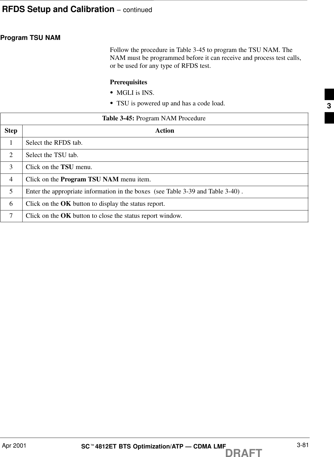
RFDS Setup and Calibration – continuedApr 2001 3-81SCt4812ET BTS Optimization/ATP — CDMA LMFDRAFTProgram TSU NAMFollow the procedure in Table 3-45 to program the TSU NAM. TheNAM must be programmed before it can receive and process test calls,or be used for any type of RFDS test.PrerequisitesSMGLI is INS.STSU is powered up and has a code load.Table 3-45: Program NAM ProcedureStep Action1Select the RFDS tab.2Select the TSU tab.3Click on the TSU menu.4Click on the Program TSU NAM menu item.5Enter the appropriate information in the boxes  (see Table 3-39 and Table 3-40) .6Click on the OK button to display the status report.7Click on the OK button to close the status report window.3
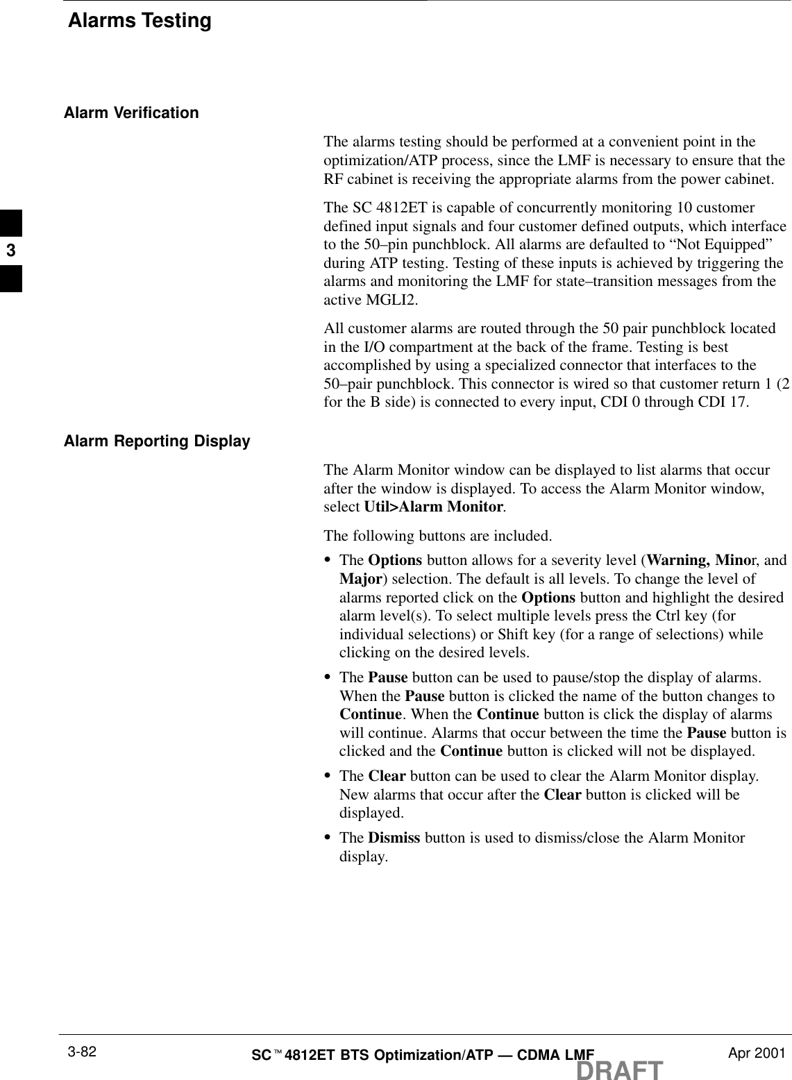
Alarms TestingDRAFTSCt4812ET BTS Optimization/ATP — CDMA LMF Apr 20013-82Alarm VerificationThe alarms testing should be performed at a convenient point in theoptimization/ATP process, since the LMF is necessary to ensure that theRF cabinet is receiving the appropriate alarms from the power cabinet.The SC 4812ET is capable of concurrently monitoring 10 customerdefined input signals and four customer defined outputs, which interfaceto the 50–pin punchblock. All alarms are defaulted to “Not Equipped”during ATP testing. Testing of these inputs is achieved by triggering thealarms and monitoring the LMF for state–transition messages from theactive MGLI2.All customer alarms are routed through the 50 pair punchblock locatedin the I/O compartment at the back of the frame. Testing is bestaccomplished by using a specialized connector that interfaces to the50–pair punchblock. This connector is wired so that customer return 1 (2for the B side) is connected to every input, CDI 0 through CDI 17.Alarm Reporting DisplayThe Alarm Monitor window can be displayed to list alarms that occurafter the window is displayed. To access the Alarm Monitor window,select Util>Alarm Monitor.The following buttons are included.SThe Options button allows for a severity level (Warning, Minor, andMajor) selection. The default is all levels. To change the level ofalarms reported click on the Options button and highlight the desiredalarm level(s). To select multiple levels press the Ctrl key (forindividual selections) or Shift key (for a range of selections) whileclicking on the desired levels.SThe Pause button can be used to pause/stop the display of alarms.When the Pause button is clicked the name of the button changes toContinue. When the Continue button is click the display of alarmswill continue. Alarms that occur between the time the Pause button isclicked and the Continue button is clicked will not be displayed.SThe Clear button can be used to clear the Alarm Monitor display.New alarms that occur after the Clear button is clicked will bedisplayed.SThe Dismiss button is used to dismiss/close the Alarm Monitordisplay.3
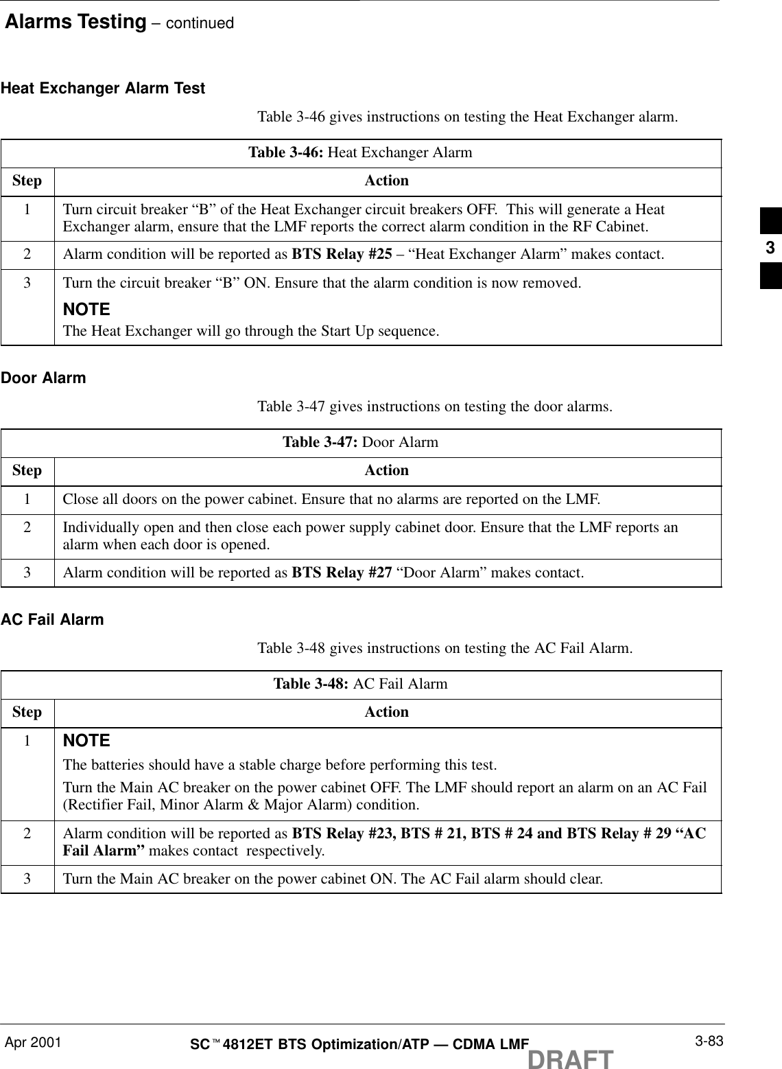
Alarms Testing – continuedApr 2001 3-83SCt4812ET BTS Optimization/ATP — CDMA LMFDRAFTHeat Exchanger Alarm TestTable 3-46 gives instructions on testing the Heat Exchanger alarm.Table 3-46: Heat Exchanger AlarmStep Action1Turn circuit breaker “B” of the Heat Exchanger circuit breakers OFF.  This will generate a HeatExchanger alarm, ensure that the LMF reports the correct alarm condition in the RF Cabinet.2Alarm condition will be reported as BTS Relay #25 – “Heat Exchanger Alarm” makes contact.3Turn the circuit breaker “B” ON. Ensure that the alarm condition is now removed.NOTEThe Heat Exchanger will go through the Start Up sequence.Door AlarmTable 3-47 gives instructions on testing the door alarms.Table 3-47: Door AlarmStep Action1Close all doors on the power cabinet. Ensure that no alarms are reported on the LMF.2Individually open and then close each power supply cabinet door. Ensure that the LMF reports analarm when each door is opened.3Alarm condition will be reported as BTS Relay #27 “Door Alarm” makes contact.AC Fail AlarmTable 3-48 gives instructions on testing the AC Fail Alarm.Table 3-48: AC Fail AlarmStep Action1NOTEThe batteries should have a stable charge before performing this test.Turn the Main AC breaker on the power cabinet OFF. The LMF should report an alarm on an AC Fail(Rectifier Fail, Minor Alarm & Major Alarm) condition.2Alarm condition will be reported as BTS Relay #23, BTS # 21, BTS # 24 and BTS Relay # 29 “ACFail Alarm” makes contact  respectively.3Turn the Main AC breaker on the power cabinet ON. The AC Fail alarm should clear.3
Alarms Testing – continuedDRAFTSCt4812ET BTS Optimization/ATP — CDMA LMF Apr 20013-84Minor Alarm  Table 3-49 gives instructions on testing minor alarm.Table 3-49: Minor AlarmStep Action1Turn the Temperature Compensation Panel (TCP) power switch OFF. This will generate a minoralarm. Verify that the minor alarm LED (amber) is illuminated on the Meter Alarm Panel and theLMF reports this minor alarm.2Alarm condition will be reported as BTS Relay #24 “Minor Alarm” makes contact.3Turn the TCP power switch ON. The alarm condition should clear.Rectifier AlarmsThe following series of tests are for single rectifier modules in a multiplerectifier system. The systems include a three rectifier and a six rectifiersystem.Single Rectifier Failure (ThreeRectifier System)Table 3-50 gives instructions on testing single rectifier failure or minoralarm in a three (3) rectifier system.Table 3-50: Single Rectifier Fail or Minor AlarmStep Action1Remove a single rectifier module and place it into the unused rectifier shelf #2.2Turn the AC breaker OFF, for this 2nd shelf.3Verify that a rectifier fail alarm is generated. The single rectifier module will illuminate two (2) REDfail LED (DC and Power), and the Meter Alarm Panel and LMF will also indicate a minor alarm andrectifier fail status. The RECTIFIER FAIL LED will illuminate.4Check that the LMF reports both of these alarm conditions.NOTEAlarm conditions reported as BTS #24 and BTS #21, contacts respectively.5Turn the AC breaker for the 2nd shelf ON and verify that Rectifier Fail and minor alarm conditionsclear on the Meter Alarm Panel and LMF. Multiple Rectifier FailureTable 3-51 gives instructions on testing multiple rectifier failure or majoralarm in a three (3) rectifier system.3
Alarms Testing – continuedApr 2001 3-85SCt4812ET BTS Optimization/ATP — CDMA LMFDRAFTTable 3-51: Multiple Rectifier Failure or Major AlarmStep Action1With the rectifier module still in the unused shelf position fromTable 3-50 test procedures, turn theAC breaker for the 1st shelf OFF.2Verify that a rectifier alarm is generated. Each of the two rectifier modules will illuminate two (2)RED fail LED (DC and Power), and the Meter Alarm Panel and LMF  will indicate a major alarm(Rectifier Fail and Major Alarm). The RECTIFIER FAIL LED will illuminate.3Verify that the LMF reports both alarm conditions. (BTS #29, BTS #21, and BTS #24)4Turn the AC breaker for the 1st shelf ON. Verify that all alarms have cleared.5Return the rectifier module to its original location. This completes the alarm test on the power cabinet. Single Rectifier Failure (Six Rectifier System)Table 3-52 gives instructions on testing single rectifier failure or minoralarm in a six (6) rectifier system.Table 3-52: Single Rectifier Fail or Minor AlarmStep Action1Remove two(2) rectifier modules from shelf #2.2Turn the AC breaker OFF, for shelf #2.3Verify that a rectifier fail alarm is generated. The single rectifier module will illuminate two (2) REDfail LED (DC and Power), and the Meter Alarm Panel and LMF will also indicate a minor alarm andrectifier fail status. The RECTIFIER FAIL LED will illuminate.4Check that the LMF reports both of these alarm conditions. (BTS #24 and BTS #21)5Turn the AC breaker for this shelf ON and verify that Rectifier Fail and Minor Alarm conditions havecleared. Multiple Rectifier Failure (SixRectifier System)Table 3-53 gives instructions on testing multiple rectifier failure or majoralarm in a six (6) rectifier system.Table 3-53: Multiple Rectifier Failure or Major AlarmStep Action1Replace one rectifier module previously removed and turn the AC breaker for  this shelf, OFF.2Verify that a rectifier alarm is generated. Each of the two rectifier modules will illuminate a RED failLED, and the Meter Alarm Panel will indicate a major alarm (Rectifier Fail, Major and MinorAlarm).The RECTIFIER FAIL LED will illuminate.. . . continued on next page3
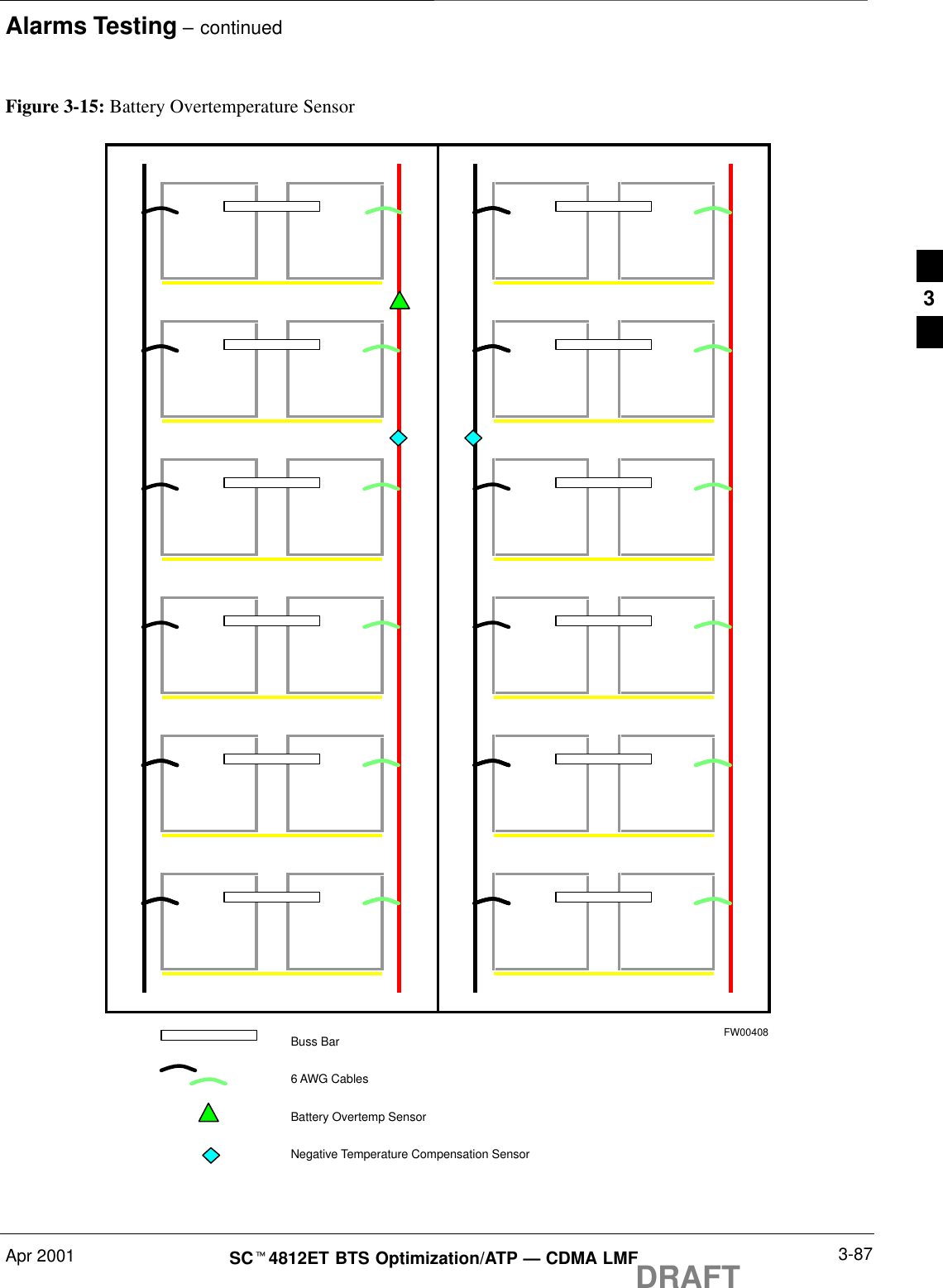
Alarms Testing – continuedDRAFTSCt4812ET BTS Optimization/ATP — CDMA LMF Apr 20013-86Table 3-53: Multiple Rectifier Failure or Major AlarmStep Action3Verify that the LMF reports both alarm conditions. (BTS #29)4Turn the AC breaker for this shelf ON. Verify that all alarms have cleared.5Return all rectifier module to their original location. This completes the rectifier alarm tests on thepower cabinet. Battery Over TemperatureAlarm (Optional)Use special care to avoid damaging insulation on cables, ordamaging battery cases when using a power heat gun.CAUTIONTable 3-54 gives instructions on testing the battery over temperaturealarm system.Table 3-54: Battery Over Temperature AlarmStep Action1Use a low powered heat gun and gently heat the battery over temperature sensor (see location inFigure 3-15). Do Not hold the hot air gun closer than three (3) inches to the sensor. This will avoidburning the cable insulation.2When the sensor is heated to approximately 50° C, a battery Over Temperature alarm is generated.NOTEAn audible click will sound as K1 contact engage and K2 contacts disengage.3Visually inspect the K1 and K2 relays to verify state changes. The LMF should be displaying correctalarms. (BTS #22)4Verify that the CHARGE DISABLE LED (amber) on the Meter Alarm Panel and the BATTERYMAIN LED (green) are both illuminated.5Switch the hot air gun to cool. Cool the sensor until the K1 and K2 contact return to normal position(K1 open and K2 closed).  Use the LMF verify that all alarms have cleared.3
Alarms Testing – continuedApr 2001 3-87SCt4812ET BTS Optimization/ATP — CDMA LMFDRAFTFigure 3-15: Battery Overtemperature SensorBuss Bar6 AWG CablesBattery Overtemp SensorNegative Temperature Compensation SensorFW004083
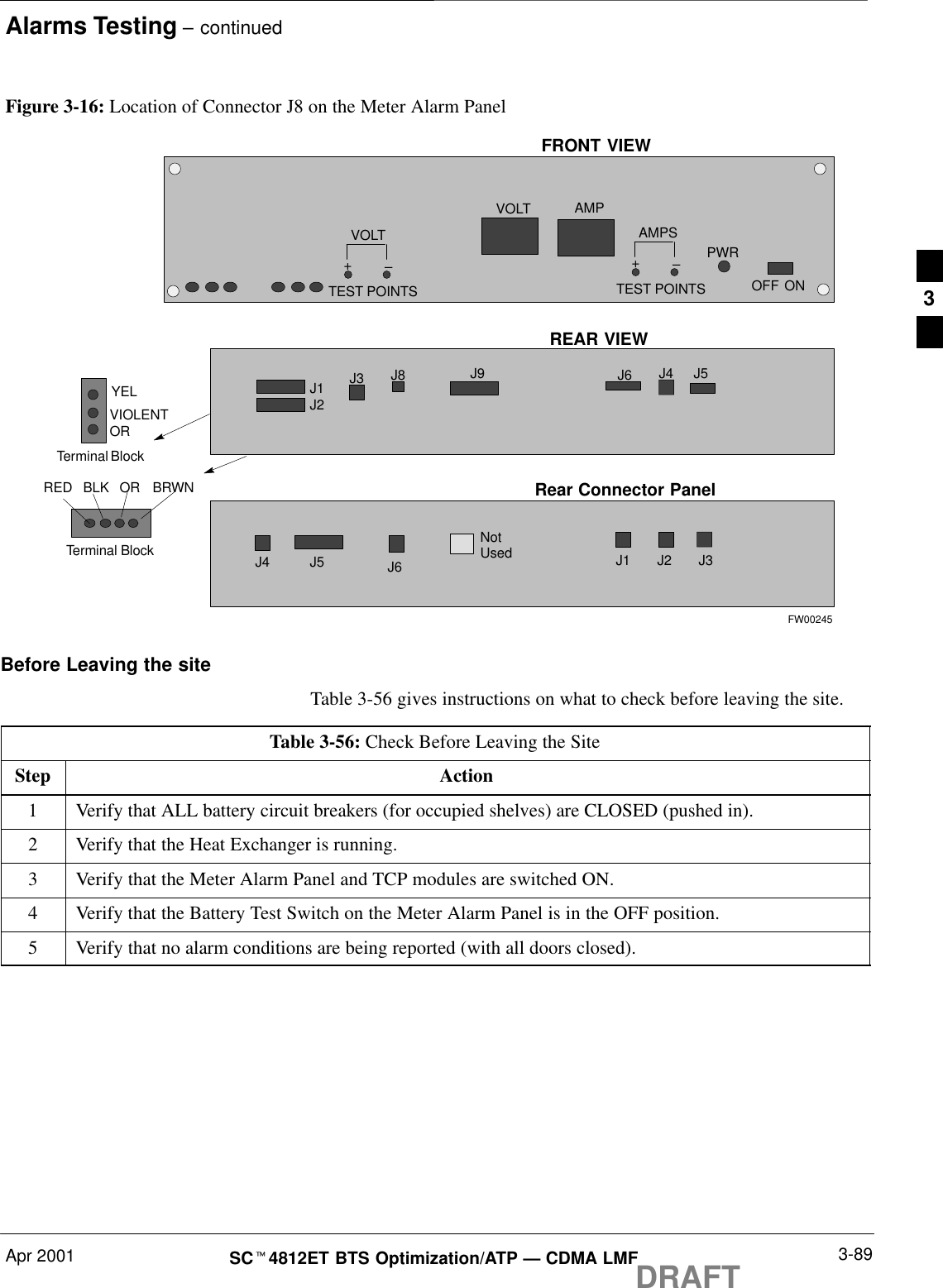
Alarms Testing – continuedDRAFTSCt4812ET BTS Optimization/ATP — CDMA LMF Apr 20013-88Rectifier Over TemperatureAlarmThis is the J8 on the rear of the Meter Alarm Panel itself,this is not connector J8 on the connector  bulkhead at therear of the cabinet.NOTETable 3-55 gives instructions on testing the battery over temperaturealarm system.Table 3-55: Rectifier Over Temperature AlarmStep Action1Remove the J8 link on the rear of the Meter Alarm Panel (see Figure 3-16 for J8 location).NOTEThis is the J8 on the rear of the Meter Alarm Panel itself, this is not connector J8 on the connectorbulkhead at the rear of the cabinet.2Verify that RECTIFIER OVERTEMP LED (red) is illuminated. Contacts on K1 and K2 change states(K1 now closed and K2 open).3Verify that the LMF has reported an alarm condition. (BTS #26)4Reinstall J8 connector and verify that all alarm conditions have cleared. K1 and K2 should now be intheir normal states (K1 open and K2 closed).5This completes the system tests of the SC 4812ET power cabinet. 3
Alarms Testing – continuedApr 2001 3-89SCt4812ET BTS Optimization/ATP — CDMA LMFDRAFTFigure 3-16: Location of Connector J8 on the Meter Alarm PanelOFFVOLTVOLT–+TEST POINTSAMPS–+TEST POINTSAMPPWRONREDYELBLKORVIOLENTOR BRWNTerminal BlockFRONT VIEWJ9J1J2J3 J8 J5J6 J4REAR VIEWTerminal BlockJ1 J2NotUsedJ6J5 J3Rear Connector PanelJ4FW00245Before Leaving the siteTable 3-56 gives instructions on what to check before leaving the site.Table 3-56: Check Before Leaving the SiteStep Action1Verify that ALL battery circuit breakers (for occupied shelves) are CLOSED (pushed in).2Verify that the Heat Exchanger is running.3Verify that the Meter Alarm Panel and TCP modules are switched ON.4Verify that the Battery Test Switch on the Meter Alarm Panel is in the OFF position.5Verify that no alarm conditions are being reported (with all doors closed).3
Alarms Testing – continuedDRAFTSCt4812ET BTS Optimization/ATP — CDMA LMF Apr 20013-90Notes3
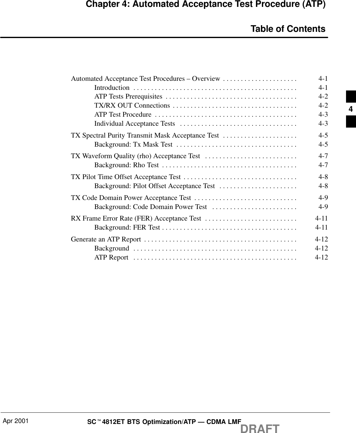
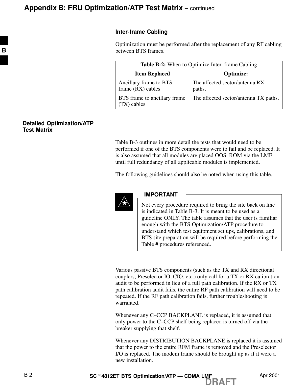
Apr 2001 SCt4812ET BTS Optimization/ATP — CDMA LMFDRAFTChapter 4: Automated Acceptance Test Procedure (ATP)Table of ContentsAutomated Acceptance Test Procedures – Overview 4-1. . . . . . . . . . . . . . . . . . . . . Introduction 4-1. . . . . . . . . . . . . . . . . . . . . . . . . . . . . . . . . . . . . . . . . . . . . . ATP Tests Prerequisites 4-2. . . . . . . . . . . . . . . . . . . . . . . . . . . . . . . . . . . . . TX/RX OUT Connections 4-2. . . . . . . . . . . . . . . . . . . . . . . . . . . . . . . . . . . ATP Test Procedure 4-3. . . . . . . . . . . . . . . . . . . . . . . . . . . . . . . . . . . . . . . . Individual Acceptance Tests 4-3. . . . . . . . . . . . . . . . . . . . . . . . . . . . . . . . . TX Spectral Purity Transmit Mask Acceptance Test 4-5. . . . . . . . . . . . . . . . . . . . . Background: Tx Mask Test 4-5. . . . . . . . . . . . . . . . . . . . . . . . . . . . . . . . . . TX Waveform Quality (rho) Acceptance Test 4-7. . . . . . . . . . . . . . . . . . . . . . . . . . Background: Rho Test 4-7. . . . . . . . . . . . . . . . . . . . . . . . . . . . . . . . . . . . . . TX Pilot Time Offset Acceptance Test 4-8. . . . . . . . . . . . . . . . . . . . . . . . . . . . . . . . Background: Pilot Offset Acceptance Test 4-8. . . . . . . . . . . . . . . . . . . . . . TX Code Domain Power Acceptance Test 4-9. . . . . . . . . . . . . . . . . . . . . . . . . . . . . Background: Code Domain Power Test 4-9. . . . . . . . . . . . . . . . . . . . . . . . RX Frame Error Rate (FER) Acceptance Test 4-11. . . . . . . . . . . . . . . . . . . . . . . . . . Background: FER Test 4-11. . . . . . . . . . . . . . . . . . . . . . . . . . . . . . . . . . . . . . Generate an ATP Report 4-12. . . . . . . . . . . . . . . . . . . . . . . . . . . . . . . . . . . . . . . . . . . Background 4-12. . . . . . . . . . . . . . . . . . . . . . . . . . . . . . . . . . . . . . . . . . . . . . ATP Report 4-12. . . . . . . . . . . . . . . . . . . . . . . . . . . . . . . . . . . . . . . . . . . . . . 4
Table of Contents  – continuedDRAFTSCt4812ET BTS Optimization/ATP — CDMA LMF Apr 2001Notes4
Automated Acceptance Test Procedures – OverviewApr 2001 4-1SCt4812ET BTS Optimization/ATP — CDMA LMFDRAFTIntroductionThe Automated Acceptance Test Procedure (ATP) allows MotorolaCellular Field Engineers (CFEs) to run automated acceptance tests on allequipped BTS subsystem devices using the Local Maintenance Facility(LMF) and supported test equipment per the current Cell Site Data File(CDF) assignment.The results of these tests (at the option of the operator) are written to afile that can be printed. All tests are controlled via the LMF platformusing the GPIB interface, therefore, only recommended test equipmentsupported by the LMF can be used.This chapter describes the tests run from the GUI environment, which isthe recommended method. The GUI provides the advantages ofsimplifying the LMF user interface, reducing the potential for miskeyingcommmands and associated parameters, and speeding up the executionof complex operations involving multiple command strings. If you feelthe command line interface (CLI) will provide additional insight into theprogress of ATPs and problems that could possibly be encountered, referto LMF CLI Commands, R15.X (68P09251A59).Before using the LMF, use an editor to view the”CAVEATS” section in the ”readme.txt” file in the c:\wlmffolder for any applicable information.The ATP test is to be performed on out-of-service sectorsonly.DO NOT substitute test equipment with other models notsupported by the LMF.IMPORTANT*Refer to Chapter 3 for detailed information on test setconnections for calibrating equipment, cables and other testset components, if  required.NOTECustomer requirements determine which ATP tests to are to beperformed and the field engineer selects the appropriate ATP tests to run.The tests can be run individually or as one of the following groups:SAll TX: TX tests verify the performance of the BTS transmit line up.These include the GLI2, MCC, BBX2, and CIO cards, the LPAs andpassive components including splitters, combiners, bandpass filter,and RF cables. . . . continued on next page4
Automated Acceptance Test Procedure – Overview  – continuedDRAFTSCt4812ET BTS Optimization/ATP — CDMA LMF Apr 20014-2SAll RX: RX tests verify the performance of the BTS receiver line up.These includes the MPC (for starter frames), EMPC (for expansionframes), CIO, BBX2, MCC, and GLI2 cards and the passivecomponents including RX filter (starter frame only), and RF cables.SAll TX/RX: Executes all the TX and RX tests.SFull Optimization: Executes the TX calibration, download BLO, andTX audit before running all of the TX and RX tests.ATP Tests PrerequisitesBefore attempting to run any ATP tests, ensure the following:SBTS has been optimized and calibrated (see Chapter 3).SLMF is logged into the BTSSCSMs, GLI2s, BBX2s, MCCs and TSU (if the RFDS is installed)have correct code load and data loadSPrimary CSM and GLI2 are INS_ACTSMCCs are INS_ACTSBBX2s are OOS-RAMSBBX2s are calibrated and BLOs are downloadedSTest cables are calibratedSTest equipment is selectedSTest equipment is connected for ATP testsSTest equipment has been warmed up 60 minutes and calibratedSGPIB is onBefore the FER is run, be sure that all LPAs are turnedOFF (circuit breakers pulled) or that all transmitter portsare properly terminated.All transmit ports must be properly terminated for all ATPtests.Failure to observe these warnings may result in bodilyinjury or equipment damage.WARNINGTX/RX OUT ConnectionsMany of the acceptance test procedures require takingmeasurements at the TX OUT (BTS/RFDS) connector. Atsites with RFDS, all measurements are through the RFDSdirectional coupler TX OUT connector.IMPORTANT*4
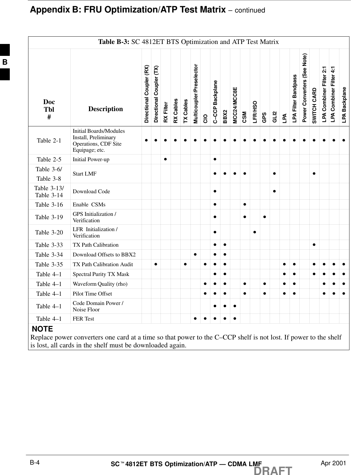
Automated Acceptance Test Procedure – Overview – continuedApr 2001 4-3SCt4812ET BTS Optimization/ATP — CDMA LMFDRAFTATP Test ProcedureThere are three different ATP testing options that can be performed tocompletely test a BTS. Depending on your requirements, one of thefollowing ATP testing options should be run.Table 4-1 provides the procedure to execute an ATP test. To completelytest a BTS, run the ATP tests according to one of the following ATPtesting options.ATP Testing Option 1SAll TX/RX testATP Testing Option 2SAll TX testSAll RX testATP Testing Option 3STX Mask testSRho testSPilot Time Offset testSCode Domain Power testSFER testThe Full Optimization test can be run if you want the TXpath calibrated before all the TX and RX tests are run.NOTEIf manual testing has been performed with the HP analyzer,remove the manual control/system memory card from thecard slot and set the IO CONFIG to the Talk & Listenmode before starting the automated testing.IMPORTANT*Individual Acceptance Tests The following individual ATP tests can be used to verify the results ofspecific tests:Spectral Purity TX MaskThis test verifies that the transmitted CDMA carrier waveform,generated on each sector, meets the transmit spectral mask specificationwith respect to the assigned CDF file values.4
Automated Acceptance Test Procedure – Overview  – continuedDRAFTSCt4812ET BTS Optimization/ATP — CDMA LMF Apr 20014-4Waveform Quality (rho)This test verifies that the transmitted Pilot channel element digitalwaveform quality (rho) exceeds the minimum specified value inANSI–J_STD–019. “Rho” represents the correlation between actual andperfect CDMA modulation spectrum. A rho value of 1.0000 represents100% (or perfect correlation).Pilot Time OffsetThe Pilot Time Offset is the difference between the CDMA analyzermeasurement interval (based on the BTS system time reference) and theincoming block of transmitted data from the BTS (Pilot only, PilotGain = 262, PN Offset = 0).Code Domain PowerThis test verifies code domain power levels, which have been set for allODD numbered Walsh channels, using the OCNS command. This isdone by verifying that the ratio of PILOT divided by OCNS is equal to10.2 + 2 dB, and, that the noise floor of all EVEN numbered “OFF”Walsh channels measures < –27 dB .Frame Error RateThe Frame Error Rate (FER) test verifies RX operation of the entireCDMA Reverse Link using all equipped MCCs assigned to allrespective sector/antennas. The test verifies the BTS sensitivity on alltraffic channel elements currently configured on all equipped MCCs atan RF input level of –119 dBm (or –116 dBm if using TMPC). Followthe procedure in Table 4-1 to perform any ATP test.The STOP button can be used to stop the testing process.NOTETable 4-1:  ATP Test ProcedureStep Action1Select the BBX2(s) and MCC(s) to be tested.2From the Tests menu, select the desired test.3Select the appropriate carrier(s) (carrier – bts# – sector# – carrier#) displayed in the Channels/Carrierpick list.To select multiple items, hold down the <Shift> or <Ctrl> key while making the selections.4Type the appropriate channel number in the Carrier n Channels box.The default channel number displayed is determined by the CdmaChans[n] number in the cbsc–n.cdffile for the BTS.5 Click OK.6Follow the cable connection directions as they are displayed.7 Click Save Results or Dismiss to close the status report window. If Dismiss is used the test results will not be saved in the test report file. 4
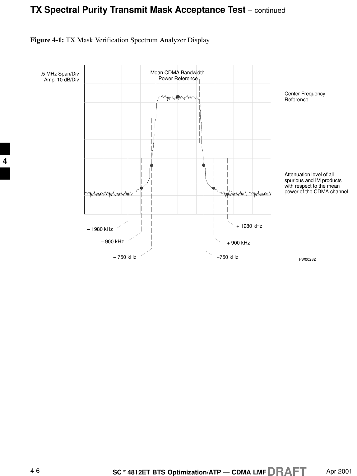
TX Spectral Purity Transmit Mask Acceptance TestApr 2001 4-5SCt4812ET BTS Optimization/ATP — CDMA LMFDRAFTBackground: Tx Mask TestThis test verifies the spectral purity of each BBX2 carrier keyed up at aspecific frequency, per the current CDF file assignment. All tests areperformed using the external calibrated test set, controlled by the samecommand. All measurements are through the appropriate TX OUT(BTS/RFDS) connector.The Pilot Gain is set to 541 for each antenna and all channel elementsfrom the MCCs are forward-link disabled. The BBX2 is keyed up, usingboth bbxlvl and bay level offsets, to generate a CDMA carrier (with pilotchannel element only). BBX2 power output is set to obtain +40 dBm asmeasured at the TX OUT connector (on either the BTS or RFDSdirectional coupler).TX output power is set to +40 dBm by setting BTS powerlevel to +33.5 dBm to compensate for 6.5 dB increase frompilot gain set to 541.NOTEThe calibrated communications test set measures and returns theattenuation level of all spurious and IM products in a 30 kHz resolutionbandwidth with respect to the mean power of the CDMA channel,measured in a 1.23 MHz bandwidth, in dB, verifying that results meetsystem tolerances at the following test points:S1.9 GHz–at least –45 dB @ + 900 kHz from center frequency–at least –45 dB @ – 900 kHz from center frequencyS800 MHz:–at least –45 dB @ + 750 kHz from center frequencY–at least –45 dB @ – 750 kHz from center frequency–at least –60 dB @ – 1980 kHz from center frequency–at least –60 dB @ – 1980 kHz from center frequencyThe BBX2 then de-keys, and, if selected, the MCC is re-configured toassign the applicable redundant BBX2 to the current TX antenna pathunder test. The test is then repeated.4
TX Spectral Purity Transmit Mask Acceptance Test – continuedDRAFTSCt4812ET BTS Optimization/ATP — CDMA LMF Apr 20014-6Figure 4-1: TX Mask Verification Spectrum Analyzer Display– 900 kHz + 900 kHzCenter FrequencyReferenceAttenuation level of allspurious and IM productswith respect to the meanpower of the CDMA channel.5 MHz Span/DivAmpl 10 dB/DivMean CDMA Bandwidth Power Reference+750 kHz+ 1980 kHz– 750 kHz– 1980 kHzFW002824
TX Waveform Quality (rho) Acceptance TestDRAFTApr 2001 4-7SCt4812ET BTS Optimization/ATP — CDMA LMFBackground: Rho TestThis test verifies the transmitted Pilot channel element digital waveformquality of each BBX2 carrier keyed up at a specific frequency per thecurrent CDF file assignment. All tests are performed using the externalcalibrated test set controlled by the same command. All measurementsare via the appropriate TX OUT (BTS/RFDS) connector.The Pilot Gain is set to 262 for each antenna, and all channel elementsfrom the MCCs will be forward link disabled. The BBX2 is keyed upusing both bbxlvl and bay level offsets, to generate a CDMA carrier(with pilot channel element only, Walsh code 0). BBX2 power output isset to 40 dBm as measured at the TX OUT connector (on either the BTSor RFDS directional coupler).The calibrated communications test set measures and returns the Pilotchannel element digital waveform quality (rho) in dB, verifying thatresult meets system tolerances Waveform quality (rho) should be > 0.912(–0.4 dB).The BBX2 then de-keys and the applicable redundant BBX2 is assignedto the current TX antenna path under test. The test is then repeated.The LMF Tests menu list item, Rho, performs the waveform quality testfor a XCVR(s). All measurements are made through the appropriate TXoutput connector using the calibrated TX cable setup.4
TX Pilot Time Offset Acceptance TestDRAFTSCt4812ET BTS Optimization/ATP — CDMA LMF Apr 20014-8Background: Pilot OffsetAcceptance TestThis test verifies the transmitted Pilot channel element Pilot Time Offsetof each BBX2 carrier keyed up at a specific frequency per the currentCDF file assignment. All tests are performed using the externalcalibrated test set controlled by the same command. All measurementswill be via the appropriate TX OUT (BTS/RFDS) connector.The Pilot Gain is set to 262 for each antenna and all TCH elements fromthe MCCs are forward link disabled. The BBX is keyed up using bothbbxlvl and bay level offsets to generate a CDMA carrier (with pilotchannel element only, Walsh code 0). BBX power output is set to40 dBm as measured at the TX OUT connector (on either the BTS orRFDS directional coupler).The calibrated communications test set measures and returns the PilotTime Offset in uS, verifying results meet system tolerances: Pilot TimeOffset should be within < 3 µs of the target PT Offset (0 mS).The BBX2 then de-keys, and the applicable redundant BBX2 is assignedto the current TX antenna path under test. The test is then repeated.4
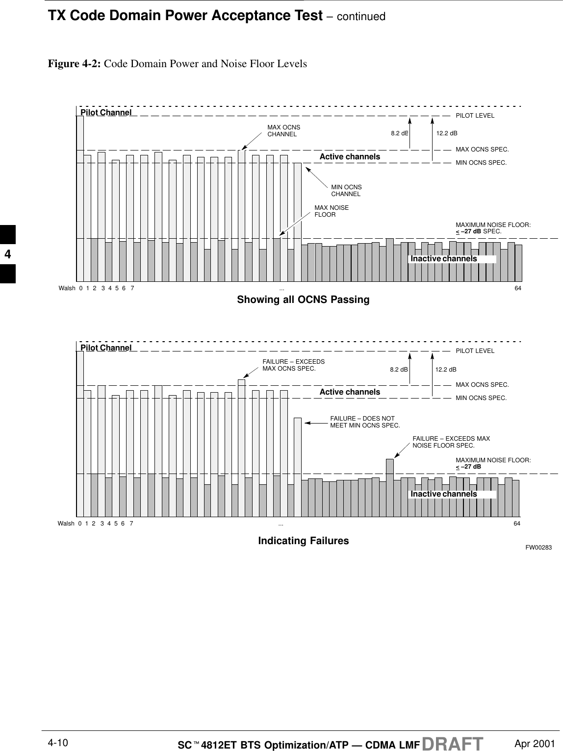
TX Code Domain Power Acceptance TestApr 2001 4-9SCt4812ET BTS Optimization/ATP — CDMA LMFDRAFTBackground: Code DomainPower TestThis test verifies the Code Domain Power/Noise of each BBX2 carrierkeyed up at a specific frequency per the current CDF file assignment.All tests are performed using the external calibrated test set controlled bythe same command. All measurements are via the appropriate TX OUT(BTS/RFDS) connector.For each sector/antenna under test, the Pilot Gain is set to 262 and allMCC channel elements under test are configured to generate OrthogonalChannel Noise Source (OCNS) on different odd Walsh codes, and areassigned a full–rate gain of 81. The maximum number of MCC/CEs tobe tested an any one time is 32 (32 odd Walsh codes). If more than 32CEs exist, then multiple sets of measurements are made, so all channelelements are verified on all sectors.BBX2 power output is set to 40 dBm as measured at the TX OUTconnector (on either the BTS or RFDS directional coupler).Code domain power levels, which have been set for all ODD numberedWalsh channels, are verified using the OCNS command. This is done byverifying that Pilot Power (dBm) minus OCNS Power (dBm) is equal to10.2 + 2 dB and that the noise floor of all “OFF” Walsh channelsmeasures  < –27 dB (with respect to total CDMA channel power).The BBX2 then de-keys and, the applicable redundant BBX2 is assignedto the current TX antenna path under test. The test is then repeated.Upon completion of the test, OCNS is disabled on the specifiedMCC/CE.4
TX Code Domain Power Acceptance Test – continuedDRAFTSCt4812ET BTS Optimization/ATP — CDMA LMF Apr 20014-10Pilot ChannelActive channelsPILOT LEVELMAX OCNS SPEC.MIN OCNS SPEC.MAXIMUM NOISE FLOOR: < –27 dB SPEC.Inactive channelsWalsh  0  1  2   3  4  5  6   7  ... 64MAX OCNSCHANNELMIN OCNSCHANNEL8.2 dB 12.2 dBMAX NOISEFLOORPilot ChannelActive channelsPILOT LEVELMAX OCNS SPEC.MIN OCNS SPEC.MAXIMUM NOISE FLOOR:< –27 dBInactive channelsWalsh  0  1  2   3  4  5  6   7  ... 64FAILURE – DOES NOTMEET MIN OCNS SPEC.FAILURE – EXCEEDSMAX OCNS SPEC. 8.2 dB 12.2 dBFAILURE – EXCEEDS MAXNOISE FLOOR SPEC. Showing all OCNS Passing Indicating FailuresFigure 4-2: Code Domain Power and Noise Floor LevelsFW002834
RX Frame Error Rate (FER) Acceptance TestApr 2001 4-11SCt4812ET BTS Optimization/ATP — CDMA LMFDRAFTBackground: FER TestThis test verifies the BTS Frame Error Rate (FER) on all traffic channelelements currently configured on all equipped MCCs (full rate at 1%FER) at an RF input level of –119 dBm [or –116 dBm if using TowerTop Amplifier (TMPC)]. All tests are performed using the externalcalibrated test set as the signal source controlled by the same command.All measurements will be via the LMF.The pilot gain is set to 262 for each TX antenna and all channel elementsfrom the MCCs are forward-link disabled. The BBX2 is keyed up usingonly bbxlvl level offsets, to generate a CDMA carrier (with pilot channelelement only). BBX2 power output is set to –20 dBm as measured at theTX OUT connector (on either the BTS or RFDS directional coupler).The BBX2 must be keyed in order to enable the RX receive circuitry.The LMF prompts the MCC/CE under test to measure all zero longcodeand provide the FER report on the selected active MCC on the reverselink for both the main and diversity RX antenna paths, verifying theresults meet the following specification: FER returned less than 1% andtotal frames measured is 1500.All MCC/CEs selected are tested on the specified RX antenna path. TheBBX then de-keys and, the applicable redundant BBX2 is assigned tothe current RX antenna paths under test. The test is then repeated.4
Generate an ATP ReportDRAFTSCt4812ET BTS Optimization/ATP — CDMA LMF Apr 20014-12BackgroundEach time an ATP test is run, an ATP report is updated to include theresults of the most recent ATP tests if the Save Results button is used toclose the status report window. The ATP report will not be updated if thestatus reports window is closed with use of the Dismiss button.ATP ReportA separate report is created for each BTS and includes the following foreach test:STest nameSBBX numberSChannel numberSCarrier numberSSector numberSUpper test limitSLower test limitSTest resultSPASS or FAILSDescription information (if applicable)STime stampSDetails/Warning information (if applicable)Follow the procedures in the Table 4-2 to view and create a printable filefor the ATP report of a BTS.Table 4-2:  Generate an ATP  Report Step Action1Click on the Login tab if it is not in the forefront.2Select the desired BTS from the Available Base Stations pick list.3Click on the Report button.4Sort the report if desired by clicking on a column heading.5Click on the Dismiss button if you do not want to create a printable file copy.6To create a printable file, select the desired file type in the picklist and then click on the Save button. 4
Apr 2001 SCt4812ET BTS Optimization/ATP — CDMA LMFDRAFTChapter 5: Leaving the SiteTable of ContentsExternal Test Equipment Removal 5-1. . . . . . . . . . . . . . . . . . . . . . . . . . . . . . . . . . . Reset All Devices 5-1. . . . . . . . . . . . . . . . . . . . . . . . . . . . . . . . . . . . . . . . . . . . . . . . Updating BTS CAL LMF Files in the CBSC 5-1. . . . . . . . . . . . . . . . . . . . . . . . . . BTS Site Span Configuration Verification 5-3. . . . . . . . . . . . . . . . . . . . . . . . . . . . . Set BTS Site Span Configuration 5-4. . . . . . . . . . . . . . . . . . . . . . . . . . . . . . . . . . . . Re–connect BTS T1 Spans and Integrated Frame Modem 5-6. . . . . . . . . . . . . . . . LMF Removal 5-6. . . . . . . . . . . . . . . . . . . . . . . . . . . . . . . . . . . . . . . . . . . . . . . . . . . Reestablish OMC-R Control/ Verifying T1/E1 5-7. . . . . . . . . . . . . . . . . . . . . . . . .  5
Table of Contents  – continuedDRAFTSCt4812ET BTS Optimization/ATP — CDMA LMF Apr 2001Notes5
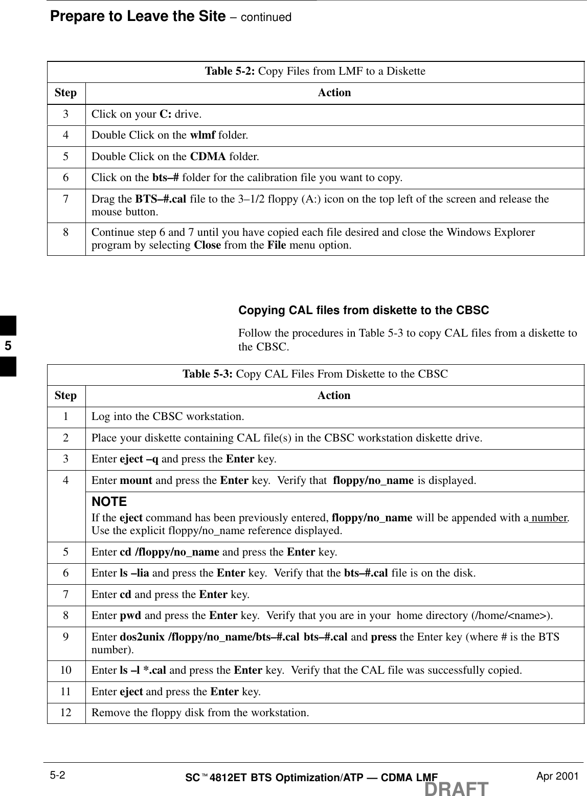
Prepare to Leave the SiteApr 2001 5-1SCt4812ET BTS Optimization/ATP — CDMA LMFDRAFTExternal Test EquipmentRemovalPerform the procedure outlined in Table 5-1 to disconnect the testequipment and configure the BTS for active service.Table 5-1: External Test Equipment RemovalStep Action1Disconnect all external test equipment from all TX and RX connectors at the rear of the frame.2Reconnect and visually inspect all TX and RX antenna feed lines at the rear of the frame.Verify all sector antenna feed lines are connected to thecorrect ports on the frame. Crossed antenna cables willcause system degradation of call processing.CAUTIONReset All DevicesReset all devices by cycling power before leaving the site. The CBSCconfiguration data and code loads could be different from data and codeon the LMF. By resetting all devices, the CBSC can load the proper dataand code when the span is active again.Updating BTS CAL LMF Filesin the CBSCUpdated CAL file information is moved from the LMF Windowsenvironment back to the CBSC which resides in a Unix environment.The procedures that follow detail how to move files from the Windowsenvironment to the CBSC.Copying CAL files from LMF to a DiskFollow the procedures in Table 5-2 to copy CAL files from a LMFcomputer to a 3.5 diskette.Table 5-2: Copy Files from LMF to a DisketteStep Action1Insert a disk into your Windows A drive.NOTEIf your disk has not been formatted, format it using Windows.  The disk must be DOS formattedbefore copying any files. Consult your Windows/DOS documentation or online helps on how toformat diskettes.2Click on the Start button and launch the Windows Explorer program from your Programs menu list.5
Prepare to Leave the Site – continuedDRAFTSCt4812ET BTS Optimization/ATP — CDMA LMF Apr 20015-2Table 5-2: Copy Files from LMF to a DisketteStep Action3Click on your C: drive.4Double Click on the wlmf folder.5Double Click on the CDMA folder.6Click on the bts–# folder for the calibration file you want to copy.7Drag the BTS–#.cal file to the 3–1/2 floppy (A:) icon on the top left of the screen and release themouse button.8Continue step 6 and 7 until you have copied each file desired and close the Windows Explorerprogram by selecting Close from the File menu option. Copying CAL files from diskette to the CBSCFollow the procedures in Table 5-3 to copy CAL files from a diskette tothe CBSC.Table 5-3: Copy CAL Files From Diskette to the CBSCStep Action1Log into the CBSC workstation.2Place your diskette containing CAL file(s) in the CBSC workstation diskette drive.3 Enter eject –q and press the Enter key.4Enter mount and press the Enter key.  Verify that  floppy/no_name is displayed.NOTEIf the eject command has been previously entered, floppy/no_name will be appended with a number.Use the explicit floppy/no_name reference displayed.5 Enter cd /floppy/no_name and press the Enter key.6 Enter ls –lia and press the Enter key.  Verify that the bts–#.cal file is on the disk.7 Enter cd and press the Enter key.8 Enter pwd and press the Enter key.  Verify that you are in your  home directory (/home/<name>).9 Enter dos2unix /floppy/no_name/bts–#.cal bts–#.cal and press the Enter key (where # is the BTSnumber).10 Enter ls –l *.cal and press the Enter key.  Verify that the CAL file was successfully copied.11 Enter eject and press the Enter key.12 Remove the floppy disk from the workstation. 5
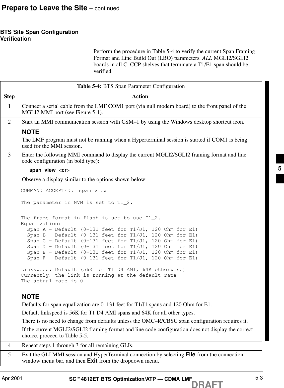
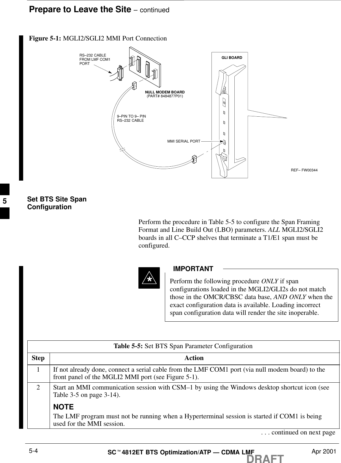
Prepare to Leave the Site – continuedApr 2001 5-3SCt4812ET BTS Optimization/ATP — CDMA LMFDRAFTBTS Site Span ConfigurationVerificationPerform the procedure in Table 5-4 to verify the current Span FramingFormat and Line Build Out (LBO) parameters. ALL MGLI2/SGLI2boards in all C–CCP shelves that terminate a T1/E1 span should beverified.Table 5-4: BTS Span Parameter ConfigurationStep Action1Connect a serial cable from the LMF COM1 port (via null modem board) to the front panel of theMGLI2 MMI port (see Figure 5-1).2Start an MMI communication session with CSM–1 by using the Windows desktop shortcut icon.NOTEThe LMF program must not be running when a Hyperterminal session is started if COM1 is beingused for the MMI session.3Enter the following MMI command to display the current MGLI2/SGLI2 framing format and linecode configuration (in bold type):span view <cr>Observe a display similar to the options shown below:COMMAND ACCEPTED: span viewThe parameter in NVM is set to T1_2.The frame format in flash is set to use T1_2.Equalization:  Span A – Default (0–131 feet for T1/J1, 120 Ohm for E1)  Span B – Default (0–131 feet for T1/J1, 120 Ohm for E1)  Span C – Default (0–131 feet for T1/J1, 120 Ohm for E1)SDD f lt (0 131 f t f T1/J1 120 Oh f E1)  Span D – Default (0–131 feet for T1/J1, 120 Ohm for E1)  Span E – Default (0–131 feet for T1/J1, 120 Ohm for E1)  Span F – Default (0–131 feet for T1/J1, 120 Ohm for E1)Linkspeed: Default (56K for T1 D4 AMI, 64K otherwise)Currently, the link is running at the default rate The actual rate is 0NOTEDefaults for span equalization are 0–131 feet for T1/J1 spans and 120 Ohm for E1.Default linkspeed is 56K for T1 D4 AMI spans and 64K for all other types.There is no need to change from defaults unless the OMC–R/CBSC span configuration requires it.If the current MGLI2/SGLI2 framing format and line code configuration does not display the correctchoice, proceed to Table 5-5.4Repeat steps 1 through 3 for all remaining GLIs.5Exit the GLI MMI session and HyperTerminal connection by selecting File from the connectionwindow menu bar, and then Exit from the dropdown menu.5
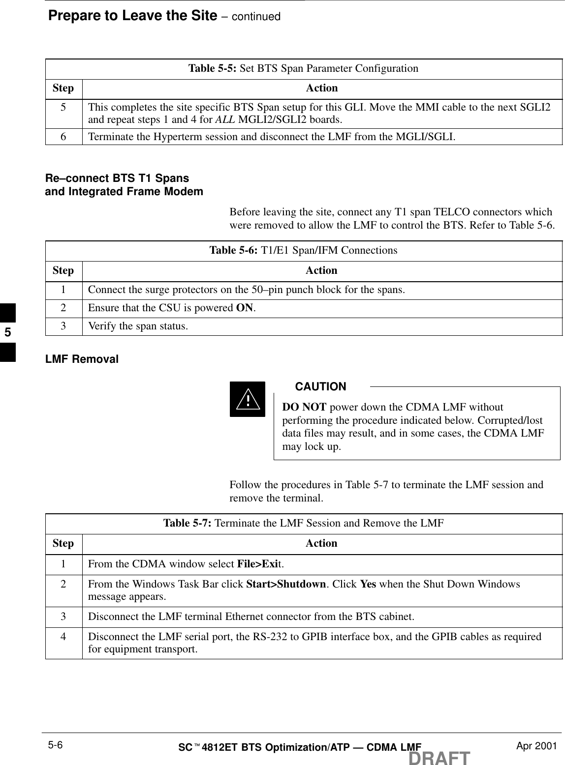
Prepare to Leave the Site – continuedDRAFTSCt4812ET BTS Optimization/ATP — CDMA LMF Apr 20015-4REF– FW003449–PIN TO 9– PINRS–232 CABLENULL MODEM BOARD(PART# 8484877P01)RS–232 CABLE FROM LMF COM1PORTMMI SERIAL PORTGLI BOARDFigure 5-1: MGLI2/SGLI2 MMI Port ConnectionSet BTS Site SpanConfigurationPerform the procedure in Table 5-5 to configure the Span FramingFormat and Line Build Out (LBO) parameters. ALL MGLI2/SGLI2boards in all C–CCP shelves that terminate a T1/E1 span must beconfigured.Perform the following procedure ONLY if spanconfigurations loaded in the MGLI2/GLI2s do not matchthose in the OMCR/CBSC data base, AND ONLY when theexact configuration data is available. Loading incorrectspan configuration data will render the site inoperable.IMPORTANT*Table 5-5: Set BTS Span Parameter ConfigurationStep Action1If not already done, connect a serial cable from the LMF COM1 port (via null modem board) to thefront panel of the MGLI2 MMI port (see Figure 5-1).2Start an MMI communication session with CSM–1 by using the Windows desktop shortcut icon (seeTable 3-5 on page 3-14).NOTEThe LMF program must not be running when a Hyperterminal session is started if COM1 is beingused for the MMI session.. . . continued on next page5
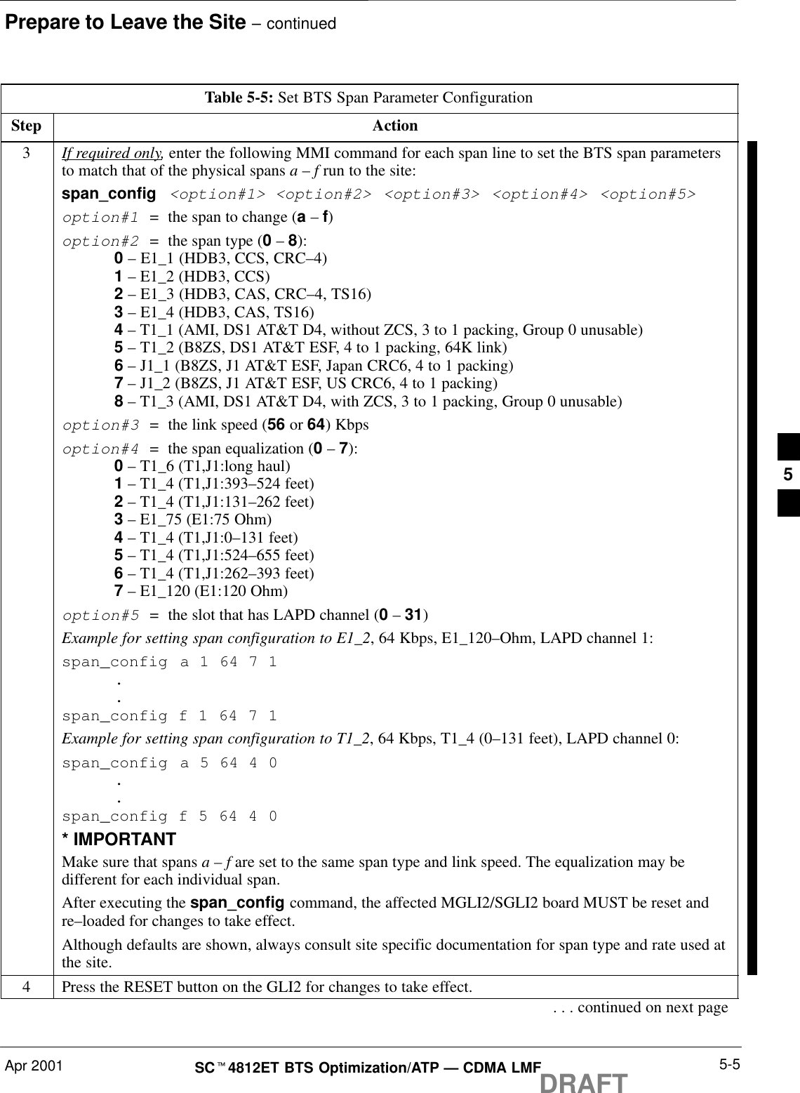
Prepare to Leave the Site – continuedApr 2001 5-5SCt4812ET BTS Optimization/ATP — CDMA LMFDRAFTTable 5-5: Set BTS Span Parameter ConfigurationStep Action3If required only, enter the following MMI command for each span line to set the BTS span parametersto match that of the physical spans a – f run to the site:span_config <option#1> <option#2> <option#3> <option#4> <option#5>option#1  =  the span to change (a – f)option#2  =  the span type (0 – 8):0 – E1_1 (HDB3, CCS, CRC–4)1 – E1_2 (HDB3, CCS)2 – E1_3 (HDB3, CAS, CRC–4, TS16)3 – E1_4 (HDB3, CAS, TS16)4 – T1_1 (AMI, DS1 AT&T D4, without ZCS, 3 to 1 packing, Group 0 unusable)5 – T1_2 (B8ZS, DS1 AT&T ESF, 4 to 1 packing, 64K link)6 – J1_1 (B8ZS, J1 AT&T ESF, Japan CRC6, 4 to 1 packing)7 – J1_2 (B8ZS, J1 AT&T ESF, US CRC6, 4 to 1 packing)8 – T1_3 (AMI, DS1 AT&T D4, with ZCS, 3 to 1 packing, Group 0 unusable)option#3  =  the link speed (56 or 64) Kbpsoption#4  =  the span equalization (0 – 7):0 – T1_6 (T1,J1:long haul)1 – T1_4 (T1,J1:393–524 feet)2 – T1_4 (T1,J1:131–262 feet)3 – E1_75 (E1:75 Ohm)4 – T1_4 (T1,J1:0–131 feet)5 – T1_4 (T1,J1:524–655 feet)6 – T1_4 (T1,J1:262–393 feet)7 – E1_120 (E1:120 Ohm)option#5  =  the slot that has LAPD channel (0 – 31)Example for setting span configuration to E1_2, 64 Kbps, E1_120–Ohm, LAPD channel 1:span_config a 1 64 7 1..span_config f 1 64 7 1Example for setting span configuration to T1_2, 64 Kbps, T1_4 (0–131 feet), LAPD channel 0:span_config a 5 64 4 0..span_config f 5 64 4 0* IMPORTANTMake sure that spans a – f are set to the same span type and link speed. The equalization may bedifferent for each individual span.After executing the span_config command, the affected MGLI2/SGLI2 board MUST be reset andre–loaded for changes to take effect.Although defaults are shown, always consult site specific documentation for span type and rate used atthe site.4Press the RESET button on the GLI2 for changes to take effect.. . . continued on next page5
Prepare to Leave the Site – continuedDRAFTSCt4812ET BTS Optimization/ATP — CDMA LMF Apr 20015-6Table 5-5: Set BTS Span Parameter ConfigurationStep Action5This completes the site specific BTS Span setup for this GLI. Move the MMI cable to the next SGLI2and repeat steps 1 and 4 for ALL MGLI2/SGLI2 boards.6Terminate the Hyperterm session and disconnect the LMF from the MGLI/SGLI. Re–connect BTS T1 Spansand Integrated Frame ModemBefore leaving the site, connect any T1 span TELCO connectors whichwere removed to allow the LMF to control the BTS. Refer to Table 5-6.Table 5-6: T1/E1 Span/IFM ConnectionsStep Action1Connect the surge protectors on the 50–pin punch block for the spans.2Ensure that the CSU is powered ON.3Verify the span status.LMF RemovalDO NOT power down the CDMA LMF withoutperforming the procedure indicated below. Corrupted/lostdata files may result, and in some cases, the CDMA LMFmay lock up.CAUTIONFollow the procedures in Table 5-7 to terminate the LMF session andremove the terminal.Table 5-7: Terminate the LMF Session and Remove the LMFStep Action1From the CDMA window select File>Exit.2From the Windows Task Bar click Start>Shutdown. Click Yes when the Shut Down Windowsmessage appears.3Disconnect the LMF terminal Ethernet connector from the BTS cabinet.4Disconnect the LMF serial port, the RS-232 to GPIB interface box, and the GPIB cables as requiredfor equipment transport.5
Prepare to Leave the Site – continuedApr 2001 5-7SCt4812ET BTS Optimization/ATP — CDMA LMFDRAFTReestablish OMC-R Control/Verifying T1/E1After all activities at the site have been completed,including disconnecting the LMF, place a phone call to theOMC-R and request the BTS be placed under control ofthe OMC-R.IMPORTANT*5
Prepare to Leave the Site – continuedDRAFTSCt4812ET BTS Optimization/ATP — CDMA LMF Apr 20015-8Notes5
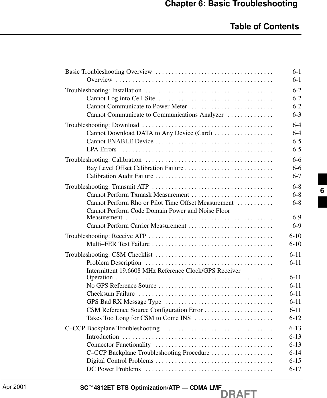
Apr 2001 SCt4812ET BTS Optimization/ATP — CDMA LMFDRAFTChapter 6: Basic TroubleshootingTable of ContentsBasic Troubleshooting Overview 6-1. . . . . . . . . . . . . . . . . . . . . . . . . . . . . . . . . . . . Overview 6-1. . . . . . . . . . . . . . . . . . . . . . . . . . . . . . . . . . . . . . . . . . . . . . . . Troubleshooting: Installation 6-2. . . . . . . . . . . . . . . . . . . . . . . . . . . . . . . . . . . . . . . Cannot Log into Cell-Site 6-2. . . . . . . . . . . . . . . . . . . . . . . . . . . . . . . . . . . Cannot Communicate to Power Meter 6-2. . . . . . . . . . . . . . . . . . . . . . . . . Cannot Communicate to Communications Analyzer 6-3. . . . . . . . . . . . . . Troubleshooting: Download 6-4. . . . . . . . . . . . . . . . . . . . . . . . . . . . . . . . . . . . . . . . Cannot Download DATA to Any Device (Card) 6-4. . . . . . . . . . . . . . . . . . Cannot ENABLE Device 6-5. . . . . . . . . . . . . . . . . . . . . . . . . . . . . . . . . . . . LPA Errors 6-5. . . . . . . . . . . . . . . . . . . . . . . . . . . . . . . . . . . . . . . . . . . . . . . Troubleshooting: Calibration 6-6. . . . . . . . . . . . . . . . . . . . . . . . . . . . . . . . . . . . . . . Bay Level Offset Calibration Failure 6-6. . . . . . . . . . . . . . . . . . . . . . . . . . . Calibration Audit Failure 6-7. . . . . . . . . . . . . . . . . . . . . . . . . . . . . . . . . . . . Troubleshooting: Transmit ATP 6-8. . . . . . . . . . . . . . . . . . . . . . . . . . . . . . . . . . . . . Cannot Perform Txmask Measurement 6-8. . . . . . . . . . . . . . . . . . . . . . . . . Cannot Perform Rho or Pilot Time Offset Measurement 6-8. . . . . . . . . . . Cannot Perform Code Domain Power and Noise FloorMeasurement 6-9. . . . . . . . . . . . . . . . . . . . . . . . . . . . . . . . . . . . . . . . . . . . . Cannot Perform Carrier Measurement 6-9. . . . . . . . . . . . . . . . . . . . . . . . . . Troubleshooting: Receive ATP 6-10. . . . . . . . . . . . . . . . . . . . . . . . . . . . . . . . . . . . . . Multi–FER Test Failure 6-10. . . . . . . . . . . . . . . . . . . . . . . . . . . . . . . . . . . . . Troubleshooting: CSM Checklist 6-11. . . . . . . . . . . . . . . . . . . . . . . . . . . . . . . . . . . . Problem Description 6-11. . . . . . . . . . . . . . . . . . . . . . . . . . . . . . . . . . . . . . . Intermittent 19.6608 MHz Reference Clock/GPS ReceiverOperation 6-11. . . . . . . . . . . . . . . . . . . . . . . . . . . . . . . . . . . . . . . . . . . . . . . . No GPS Reference Source 6-11. . . . . . . . . . . . . . . . . . . . . . . . . . . . . . . . . . . Checksum Failure 6-11. . . . . . . . . . . . . . . . . . . . . . . . . . . . . . . . . . . . . . . . . GPS Bad RX Message Type 6-11. . . . . . . . . . . . . . . . . . . . . . . . . . . . . . . . . CSM Reference Source Configuration Error 6-11. . . . . . . . . . . . . . . . . . . . . Takes Too Long for CSM to Come INS 6-12. . . . . . . . . . . . . . . . . . . . . . . . C–CCP Backplane Troubleshooting 6-13. . . . . . . . . . . . . . . . . . . . . . . . . . . . . . . . . . Introduction 6-13. . . . . . . . . . . . . . . . . . . . . . . . . . . . . . . . . . . . . . . . . . . . . . Connector Functionality 6-13. . . . . . . . . . . . . . . . . . . . . . . . . . . . . . . . . . . . C–CCP Backplane Troubleshooting Procedure 6-14. . . . . . . . . . . . . . . . . . . Digital Control Problems 6-15. . . . . . . . . . . . . . . . . . . . . . . . . . . . . . . . . . . . DC Power Problems 6-17. . . . . . . . . . . . . . . . . . . . . . . . . . . . . . . . . . . . . . . 6
Table of Contents  – continuedDRAFTSCt4812ET BTS Optimization/ATP — CDMA LMF Apr 2001RFDS – Fault Isolation 6-19. . . . . . . . . . . . . . . . . . . . . . . . . . . . . . . . . . . . . . . . . . . . Introduction 6-19. . . . . . . . . . . . . . . . . . . . . . . . . . . . . . . . . . . . . . . . . . . . . . All tests fail 6-19. . . . . . . . . . . . . . . . . . . . . . . . . . . . . . . . . . . . . . . . . . . . . . All RX and TX paths fail 6-19. . . . . . . . . . . . . . . . . . . . . . . . . . . . . . . . . . . . All tests fail on a single antenna 6-20. . . . . . . . . . . . . . . . . . . . . . . . . . . . . . Module Front Panel LED Indicators and Connectors 6-21. . . . . . . . . . . . . . . . . . . . . Module Status Indicators 6-21. . . . . . . . . . . . . . . . . . . . . . . . . . . . . . . . . . . . LED Status Combinations for All Modules (except GLI2,CSM, BBX2, MCC24E, MCC8E) 6-21. . . . . . . . . . . . . . . . . . . . . . . . . . . . DC/DC Converter LED Status Combinations 6-21. . . . . . . . . . . . . . . . . . . . CSM LED Status Combinations 6-22. . . . . . . . . . . . . . . . . . . . . . . . . . . . . . GLI2 LED Status Combinations 6-24. . . . . . . . . . . . . . . . . . . . . . . . . . . . . . GLI2 Pushbuttons and Connectors 6-25. . . . . . . . . . . . . . . . . . . . . . . . . . . . BBX2 LED Status Combinations 6-26. . . . . . . . . . . . . . . . . . . . . . . . . . . . . MCC24/MCC8E LED Status Combinations 6-26. . . . . . . . . . . . . . . . . . . . . LPA Shelf LED Status Combinations 6-27. . . . . . . . . . . . . . . . . . . . . . . . . . Basic Troubleshooting – Span Control Link 6-28. . . . . . . . . . . . . . . . . . . . . . . . . . . Span Problems (No Control Link) 6-28. . . . . . . . . . . . . . . . . . . . . . . . . . . . .  6
Basic Troubleshooting OverviewApr 2001 6-1SCt4812ET BTS Optimization/ATP — CDMA LMFDRAFTOverviewThe information in this chapter addresses some of the scenarios likely tobe encountered by Customer Field Engineering (CFE) team members.This troubleshooting guide was created as an interim reference documentfor use in the field. It provides basic “what to do if” basictroubleshooting suggestions when the BTS equipment does not performper the procedure documented in the manual.Comments are consolidated from inputs provided by CFEs in the fieldand information gained form experience in Motorola labs andclassrooms.6
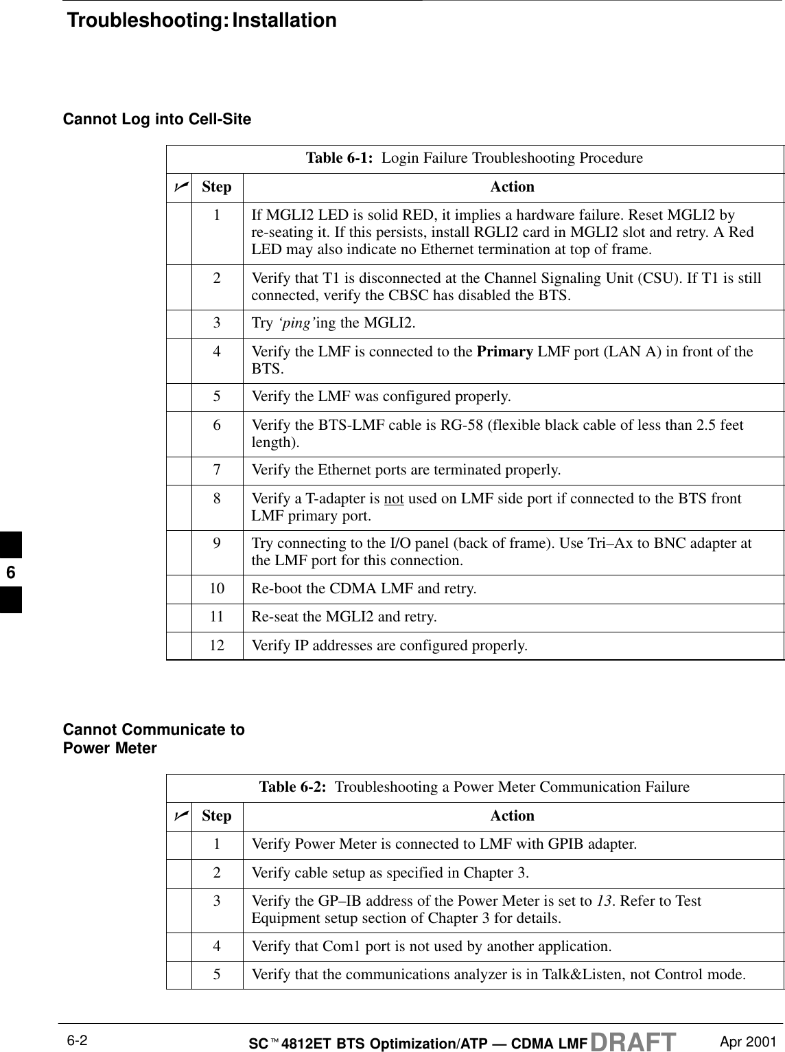
Troubleshooting: InstallationDRAFTSCt4812ET BTS Optimization/ATP — CDMA LMF Apr 20016-2Cannot Log into Cell-SiteTable 6-1:  Login Failure Troubleshooting ProcedurenStep Action1If MGLI2 LED is solid RED, it implies a hardware failure. Reset MGLI2 byre-seating it. If this persists, install RGLI2 card in MGLI2 slot and retry. A RedLED may also indicate no Ethernet termination at top of frame.2Verify that T1 is disconnected at the Channel Signaling Unit (CSU). If T1 is stillconnected, verify the CBSC has disabled the BTS.3Try ‘ping’ing the MGLI2.4Verify the LMF is connected to the Primary LMF port (LAN A) in front of theBTS.5Verify the LMF was configured properly.6Verify the BTS-LMF cable is RG-58 (flexible black cable of less than 2.5 feetlength).7Verify the Ethernet ports are terminated properly.8Verify a T-adapter is not used on LMF side port if connected to the BTS frontLMF primary port.9Try connecting to the I/O panel (back of frame). Use Tri–Ax to BNC adapter atthe LMF port for this connection.10 Re-boot the CDMA LMF and retry.11 Re-seat the MGLI2 and retry.12 Verify IP addresses are configured properly. Cannot Communicate toPower MeterTable 6-2:  Troubleshooting a Power Meter Communication FailurenStep Action1Verify Power Meter is connected to LMF with GPIB adapter.2Verify cable setup as specified in Chapter 3.3Verify the GP–IB address of the Power Meter is set to 13. Refer to TestEquipment setup section of Chapter 3 for details.4Verify that Com1 port is not used by another application.5Verify that the communications analyzer is in Talk&Listen, not Control mode. 6
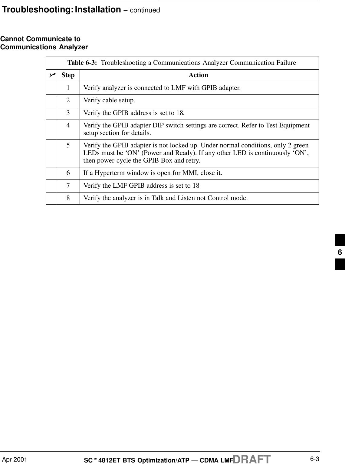
Troubleshooting: Installation – continuedApr 2001 6-3SCt4812ET BTS Optimization/ATP — CDMA LMFDRAFTCannot Communicate toCommunications AnalyzerTable 6-3:  Troubleshooting a Communications Analyzer Communication FailurenStep Action1Verify analyzer is connected to LMF with GPIB adapter.2Verify cable setup.3Verify the GPIB address is set to 18.4Verify the GPIB adapter DIP switch settings are correct. Refer to Test Equipmentsetup section for details.5Verify the GPIB adapter is not locked up. Under normal conditions, only 2 greenLEDs must be ‘ON’ (Power and Ready). If any other LED is continuously ‘ON’,then power-cycle the GPIB Box and retry.6If a Hyperterm window is open for MMI, close it.7Verify the LMF GPIB address is set to 188Verify the analyzer is in Talk and Listen not Control mode. 6
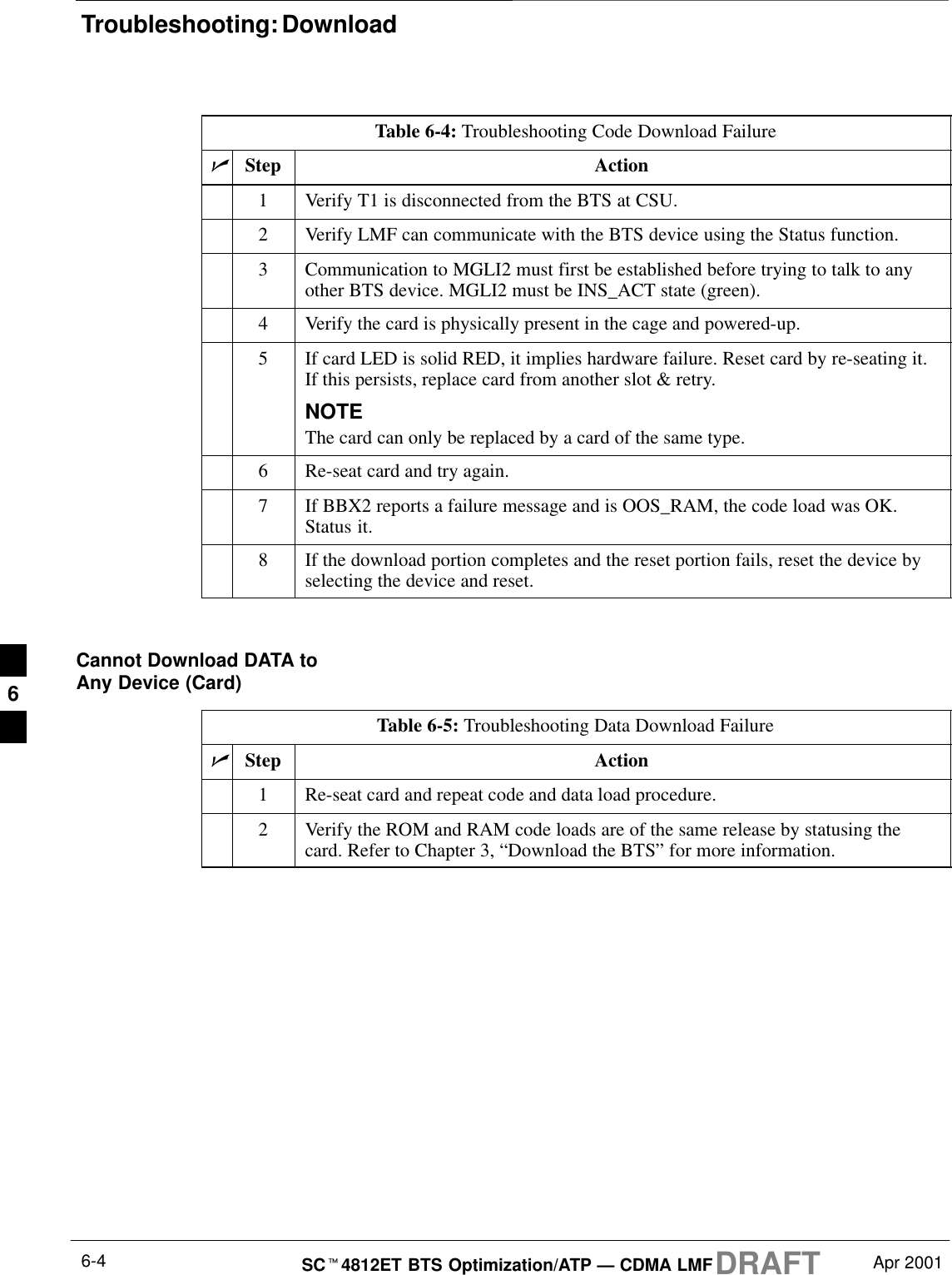
Troubleshooting: DownloadDRAFTSCt4812ET BTS Optimization/ATP — CDMA LMF Apr 20016-4Table 6-4: Troubleshooting Code Download FailurenStep Action1Verify T1 is disconnected from the BTS at CSU.2Verify LMF can communicate with the BTS device using the Status function.3Communication to MGLI2 must first be established before trying to talk to anyother BTS device. MGLI2 must be INS_ACT state (green).4Verify the card is physically present in the cage and powered-up.5If card LED is solid RED, it implies hardware failure. Reset card by re-seating it.If this persists, replace card from another slot & retry.NOTEThe card can only be replaced by a card of the same type.6Re-seat card and try again.7If BBX2 reports a failure message and is OOS_RAM, the code load was OK.Status it.8If the download portion completes and the reset portion fails, reset the device byselecting the device and reset. Cannot Download DATA toAny Device (Card)Table 6-5: Troubleshooting Data Download FailurenStep Action1Re-seat card and repeat code and data load procedure.2Verify the ROM and RAM code loads are of the same release by statusing thecard. Refer to Chapter 3, “Download the BTS” for more information.6
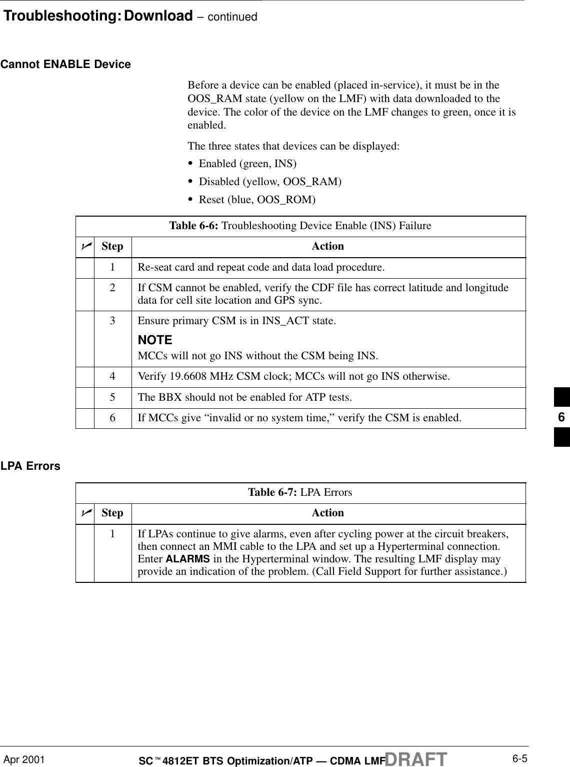
Troubleshooting: Download – continuedApr 2001 6-5SCt4812ET BTS Optimization/ATP — CDMA LMFDRAFTCannot ENABLE DeviceBefore a device can be enabled (placed in-service), it must be in theOOS_RAM state (yellow on the LMF) with data downloaded to thedevice. The color of the device on the LMF changes to green, once it isenabled.The three states that devices can be displayed:SEnabled (green, INS)SDisabled (yellow, OOS_RAM)SReset (blue, OOS_ROM)Table 6-6: Troubleshooting Device Enable (INS) FailurenStep Action1Re-seat card and repeat code and data load procedure.2If CSM cannot be enabled, verify the CDF file has correct latitude and longitudedata for cell site location and GPS sync.3Ensure primary CSM is in INS_ACT state.NOTEMCCs will not go INS without the CSM being INS.4Verify 19.6608 MHz CSM clock; MCCs will not go INS otherwise.5The BBX should not be enabled for ATP tests.6If MCCs give “invalid or no system time,” verify the CSM is enabled. LPA ErrorsTable 6-7: LPA ErrorsnStep Action1If LPAs continue to give alarms, even after cycling power at the circuit breakers,then connect an MMI cable to the LPA and set up a Hyperterminal connection.Enter ALARMS in the Hyperterminal window. The resulting LMF display mayprovide an indication of the problem. (Call Field Support for further assistance.)6
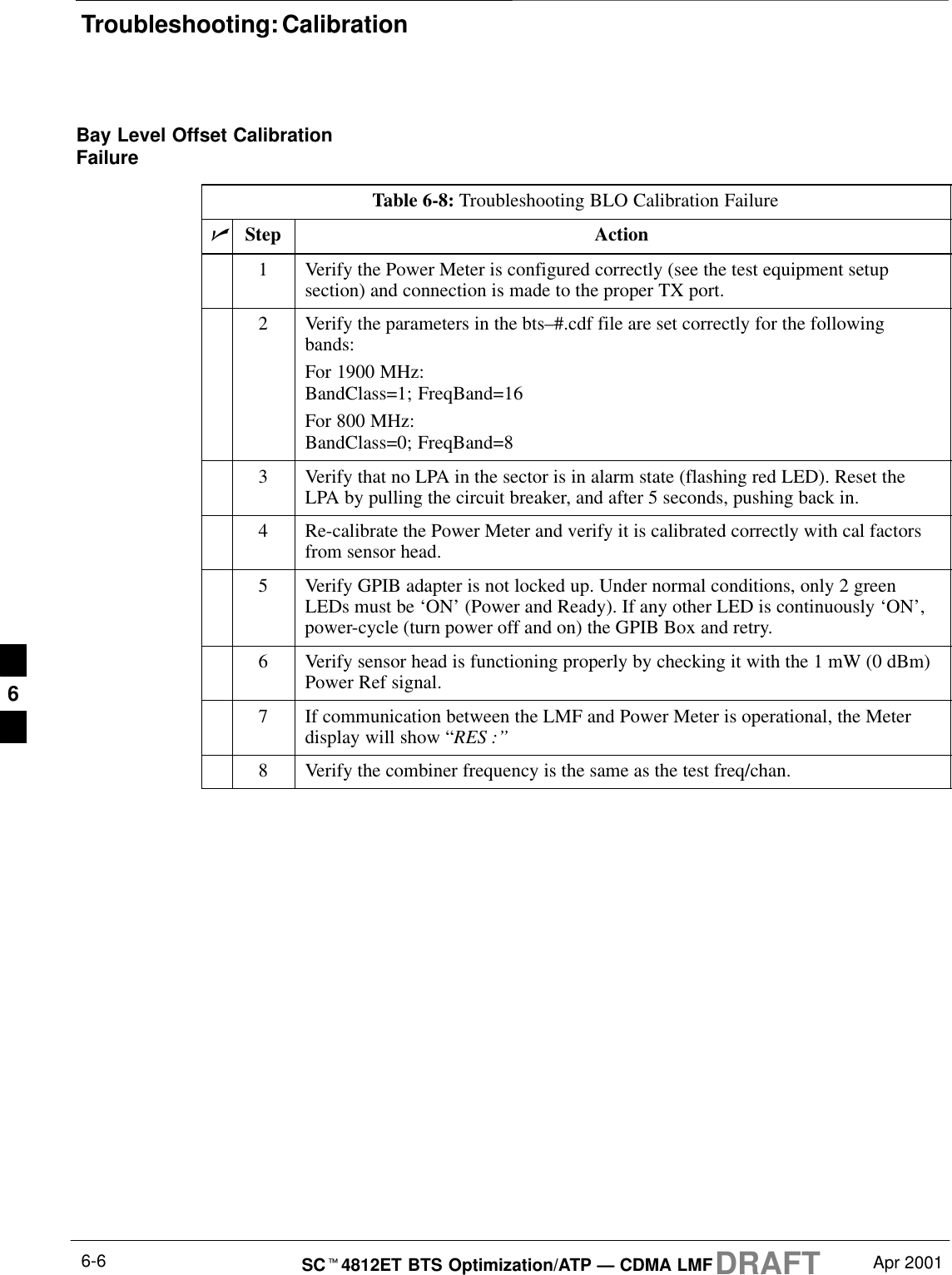
Troubleshooting: CalibrationDRAFTSCt4812ET BTS Optimization/ATP — CDMA LMF Apr 20016-6Bay Level Offset CalibrationFailureTable 6-8: Troubleshooting BLO Calibration FailurenStep Action1Verify the Power Meter is configured correctly (see the test equipment setupsection) and connection is made to the proper TX port.2Verify the parameters in the bts–#.cdf file are set correctly for the followingbands:For 1900 MHz:BandClass=1; FreqBand=16For 800 MHz:BandClass=0; FreqBand=83Verify that no LPA in the sector is in alarm state (flashing red LED). Reset theLPA by pulling the circuit breaker, and after 5 seconds, pushing back in.4Re-calibrate the Power Meter and verify it is calibrated correctly with cal factorsfrom sensor head.5Verify GPIB adapter is not locked up. Under normal conditions, only 2 greenLEDs must be ‘ON’ (Power and Ready). If any other LED is continuously ‘ON’,power-cycle (turn power off and on) the GPIB Box and retry.6Verify sensor head is functioning properly by checking it with the 1 mW (0 dBm)Power Ref signal.7If communication between the LMF and Power Meter is operational, the Meterdisplay will show “RES :’’8Verify the combiner frequency is the same as the test freq/chan. 6
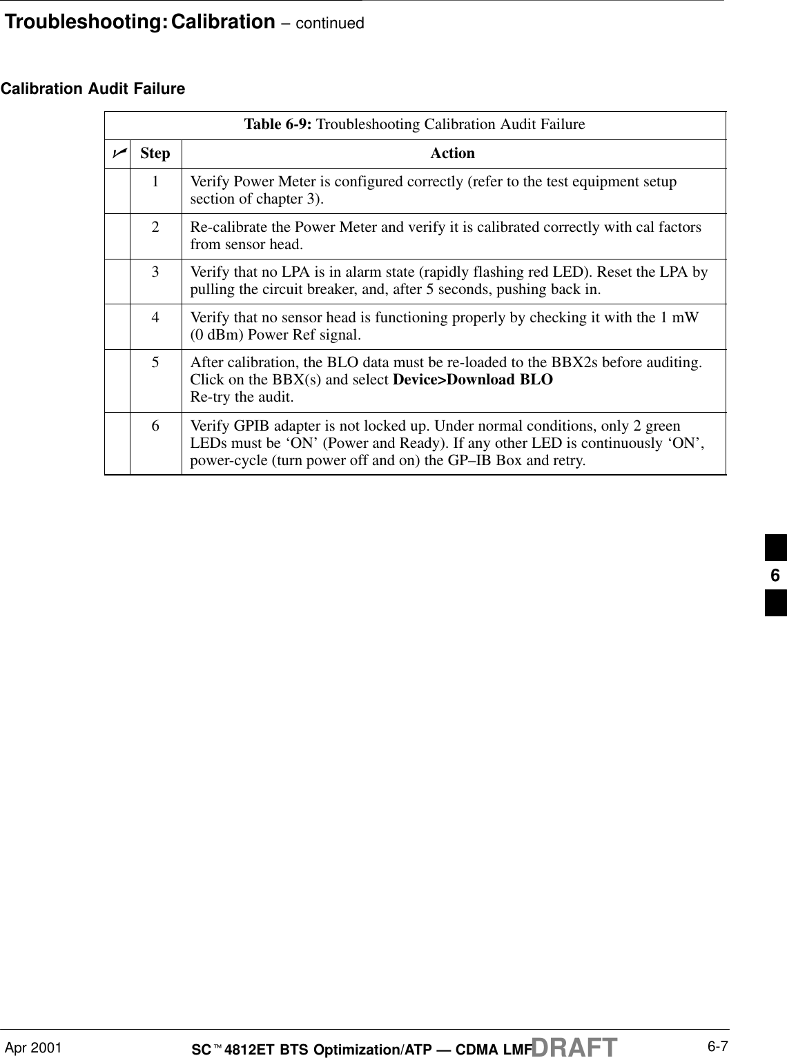
Troubleshooting: Calibration – continuedApr 2001 6-7SCt4812ET BTS Optimization/ATP — CDMA LMFDRAFTCalibration Audit FailureTable 6-9: Troubleshooting Calibration Audit FailurenStep Action1Verify Power Meter is configured correctly (refer to the test equipment setupsection of chapter 3).2Re-calibrate the Power Meter and verify it is calibrated correctly with cal factorsfrom sensor head.3Verify that no LPA is in alarm state (rapidly flashing red LED). Reset the LPA bypulling the circuit breaker, and, after 5 seconds, pushing back in.4Verify that no sensor head is functioning properly by checking it with the 1 mW(0 dBm) Power Ref signal.5After calibration, the BLO data must be re-loaded to the BBX2s before auditing.Click on the BBX(s) and select Device>Download BLORe-try the audit.6Verify GPIB adapter is not locked up. Under normal conditions, only 2 greenLEDs must be ‘ON’ (Power and Ready). If any other LED is continuously ‘ON’,power-cycle (turn power off and on) the GP–IB Box and retry. 6
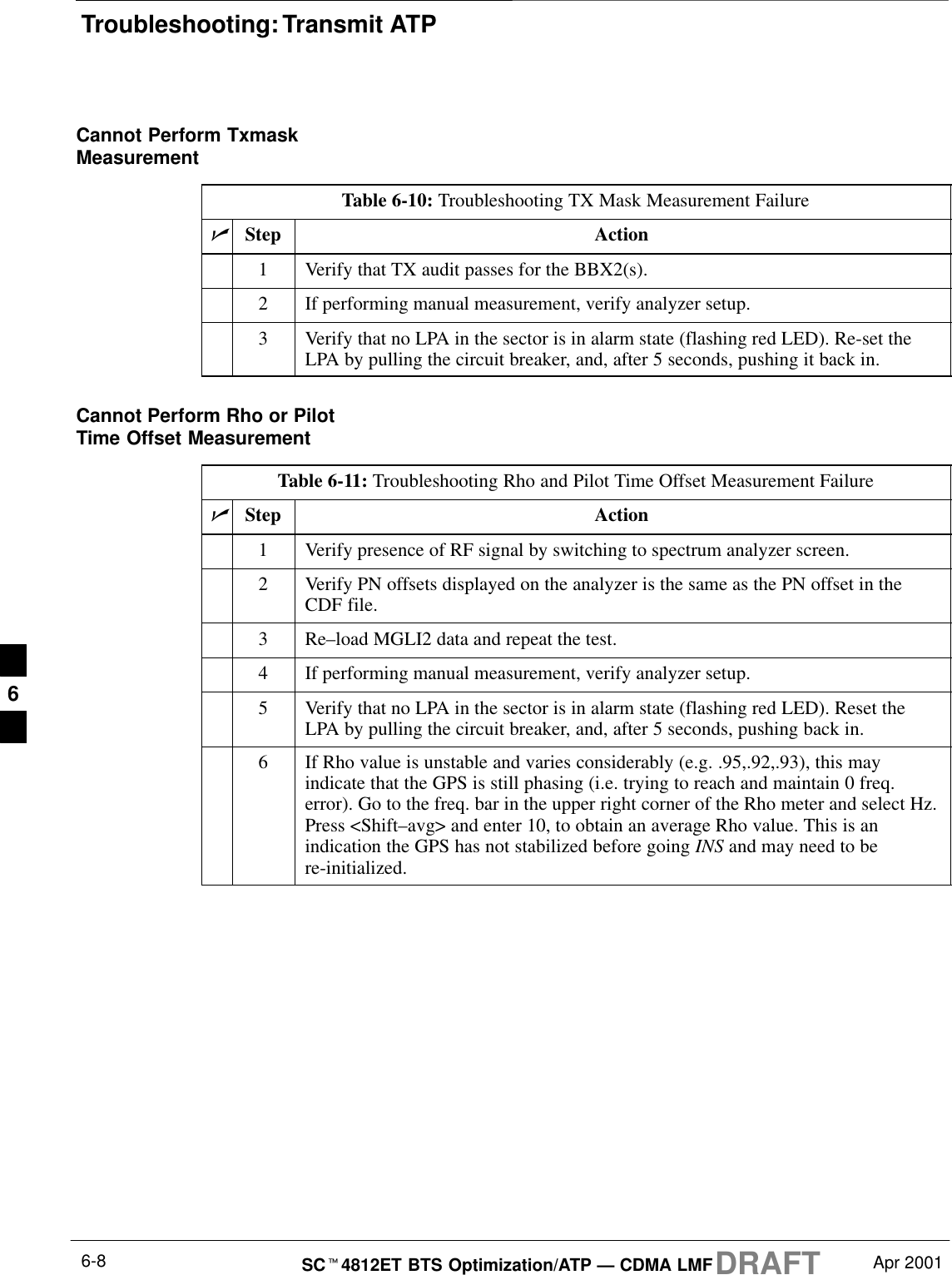
Troubleshooting: Transmit ATPDRAFTSCt4812ET BTS Optimization/ATP — CDMA LMF Apr 20016-8Cannot Perform TxmaskMeasurementTable 6-10: Troubleshooting TX Mask Measurement FailurenStep Action1Verify that TX audit passes for the BBX2(s).2If performing manual measurement, verify analyzer setup.3Verify that no LPA in the sector is in alarm state (flashing red LED). Re-set theLPA by pulling the circuit breaker, and, after 5 seconds, pushing it back in.Cannot Perform Rho or PilotTime Offset MeasurementTable 6-11: Troubleshooting Rho and Pilot Time Offset Measurement FailurenStep Action1Verify presence of RF signal by switching to spectrum analyzer screen.2Verify PN offsets displayed on the analyzer is the same as the PN offset in theCDF file.3 Re–load MGLI2 data and repeat the test.4If performing manual measurement, verify analyzer setup.5Verify that no LPA in the sector is in alarm state (flashing red LED). Reset theLPA by pulling the circuit breaker, and, after 5 seconds, pushing back in.6If Rho value is unstable and varies considerably (e.g. .95,.92,.93), this mayindicate that the GPS is still phasing (i.e. trying to reach and maintain 0 freq.error). Go to the freq. bar in the upper right corner of the Rho meter and select Hz.Press <Shift–avg> and enter 10, to obtain an average Rho value. This is anindication the GPS has not stabilized before going INS and may need to bere-initialized. 6
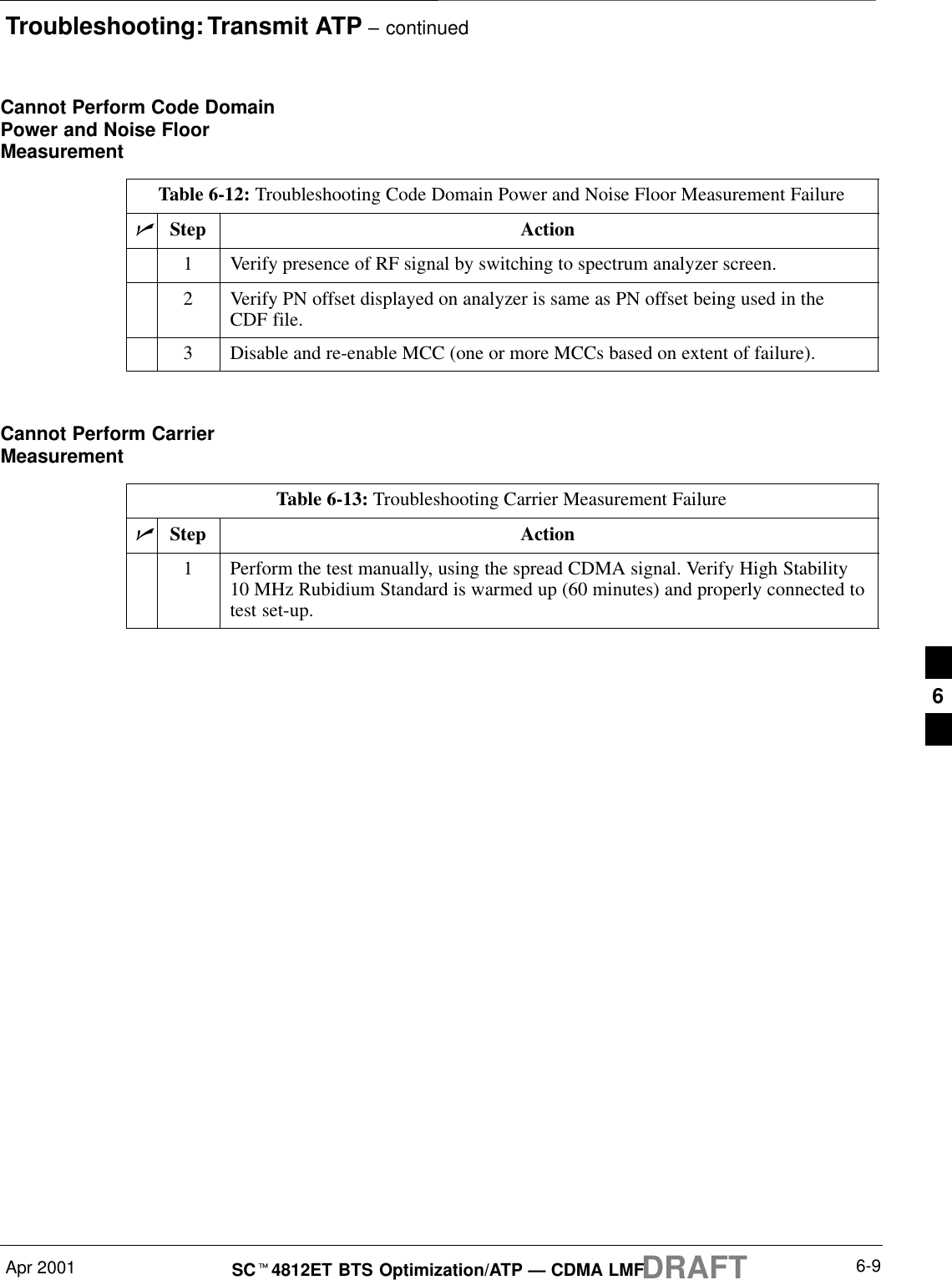
Troubleshooting: Transmit ATP – continuedApr 2001 6-9SCt4812ET BTS Optimization/ATP — CDMA LMFDRAFTCannot Perform Code DomainPower and Noise FloorMeasurementTable 6-12: Troubleshooting Code Domain Power and Noise Floor Measurement FailurenStep Action1Verify presence of RF signal by switching to spectrum analyzer screen.2Verify PN offset displayed on analyzer is same as PN offset being used in theCDF file.3Disable and re-enable MCC (one or more MCCs based on extent of failure). Cannot Perform CarrierMeasurementTable 6-13: Troubleshooting Carrier Measurement FailurenStep Action1Perform the test manually, using the spread CDMA signal. Verify High Stability10 MHz Rubidium Standard is warmed up (60 minutes) and properly connected totest set-up.6
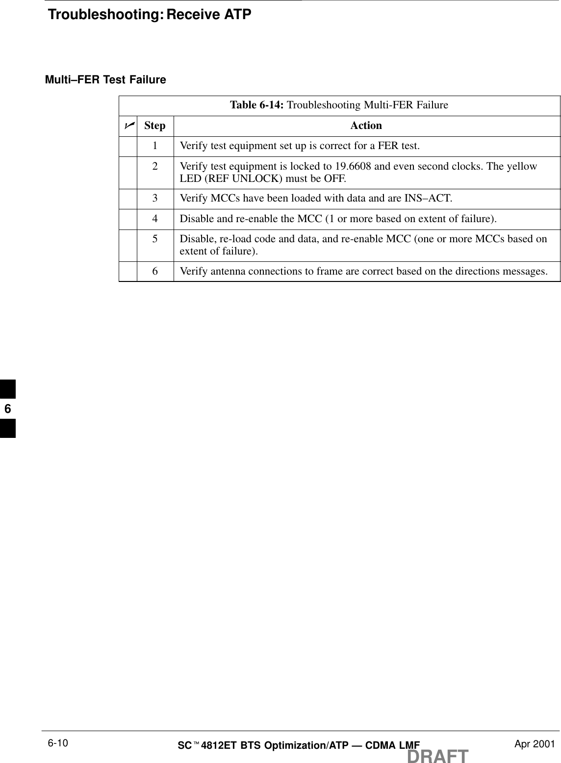
Troubleshooting: Receive ATPDRAFTSCt4812ET BTS Optimization/ATP — CDMA LMF Apr 20016-10Multi–FER Test FailureTable 6-14: Troubleshooting Multi-FER FailurenStep Action1Verify test equipment set up is correct for a FER test.2Verify test equipment is locked to 19.6608 and even second clocks. The yellowLED (REF UNLOCK) must be OFF.3Verify MCCs have been loaded with data and are INS–ACT.4Disable and re-enable the MCC (1 or more based on extent of failure).5Disable, re-load code and data, and re-enable MCC (one or more MCCs based onextent of failure).6Verify antenna connections to frame are correct based on the directions messages. 6
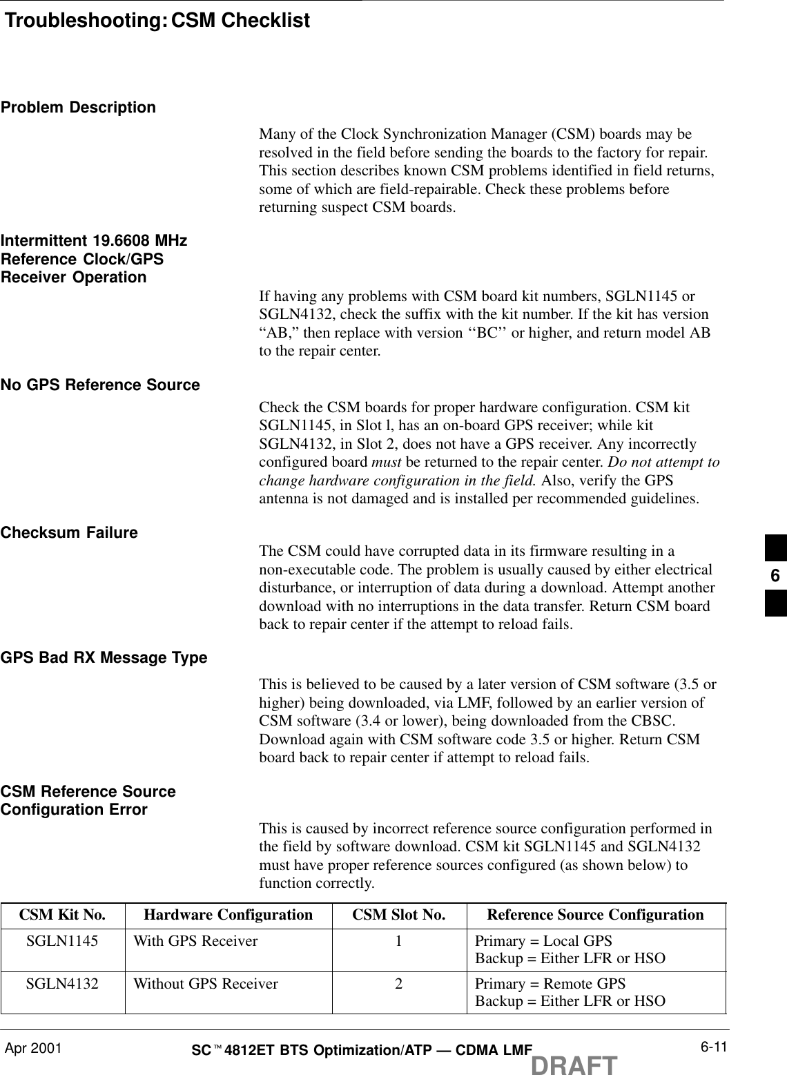
Troubleshooting: CSM ChecklistApr 2001 6-11SCt4812ET BTS Optimization/ATP — CDMA LMFDRAFTProblem DescriptionMany of the Clock Synchronization Manager (CSM) boards may beresolved in the field before sending the boards to the factory for repair.This section describes known CSM problems identified in field returns,some of which are field-repairable. Check these problems beforereturning suspect CSM boards.Intermittent 19.6608 MHzReference Clock/GPSReceiver Operation If having any problems with CSM board kit numbers, SGLN1145 orSGLN4132, check the suffix with the kit number. If the kit has version“AB,” then replace with version ‘‘BC’’ or higher, and return model ABto the repair center.No GPS Reference SourceCheck the CSM boards for proper hardware configuration. CSM kitSGLN1145, in Slot l, has an on-board GPS receiver; while kitSGLN4132, in Slot 2, does not have a GPS receiver. Any incorrectlyconfigured board must be returned to the repair center. Do not attempt tochange hardware configuration in the field. Also, verify the GPSantenna is not damaged and is installed per recommended guidelines.Checksum Failure The CSM could have corrupted data in its firmware resulting in anon-executable code. The problem is usually caused by either electricaldisturbance, or interruption of data during a download. Attempt anotherdownload with no interruptions in the data transfer. Return CSM boardback to repair center if the attempt to reload fails.GPS Bad RX Message TypeThis is believed to be caused by a later version of CSM software (3.5 orhigher) being downloaded, via LMF, followed by an earlier version ofCSM software (3.4 or lower), being downloaded from the CBSC.Download again with CSM software code 3.5 or higher. Return CSMboard back to repair center if attempt to reload fails.CSM Reference SourceConfiguration Error This is caused by incorrect reference source configuration performed inthe field by software download. CSM kit SGLN1145 and SGLN4132must have proper reference sources configured (as shown below) tofunction correctly.CSM Kit No. Hardware Configuration CSM Slot No. Reference Source ConfigurationSGLN1145 With GPS Receiver 1Primary = Local GPSBackup = Either LFR or HSOSGLN4132 Without GPS Receiver 2Primary = Remote GPSBackup = Either LFR or HSO6
Troubleshooting: CSM Checklist – continuedDRAFTSCt4812ET BTS Optimization/ATP — CDMA LMF Apr 20016-12Takes Too Long for CSM toCome INSThis may be caused by a delay in GPS acquisition. Check the accuracyflag status and/or current position. Refer to the GSM system time/GPSand LFR/HSO verification section in Chapter 3. At least 1 satelliteshould be visible and tracked for the “surveyed” mode and 4 satellitesshould be visible and tracked for the “estimated” mode. Also, verifycorrect base site position data used in “surveyed” mode.6
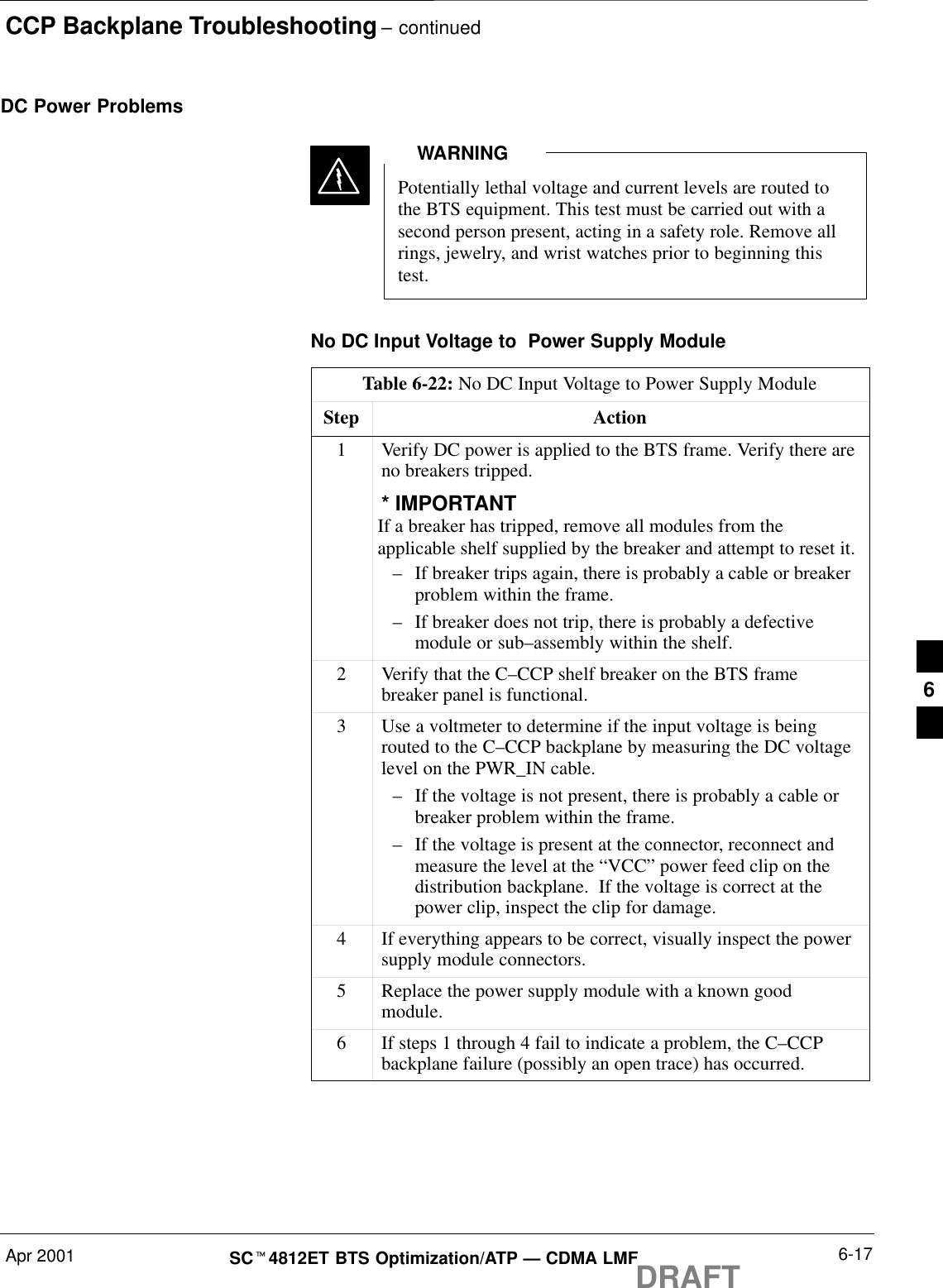
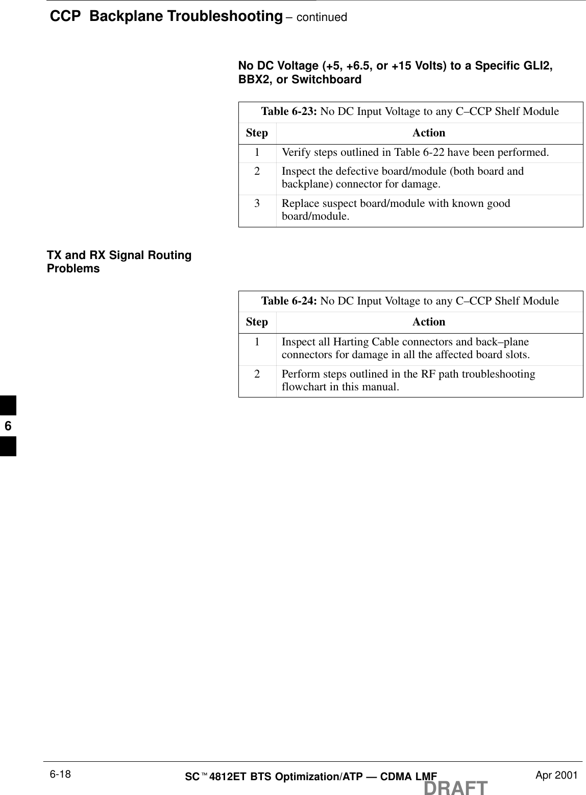
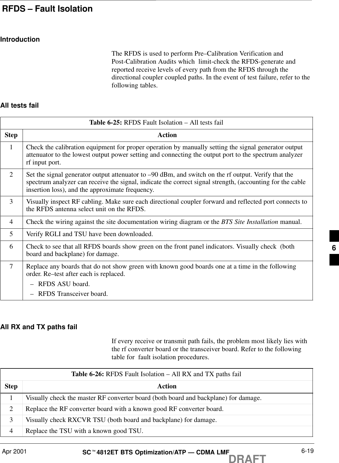
C–CCP Backplane TroubleshootingApr 2001 6-13SCt4812ET BTS Optimization/ATP — CDMA LMFDRAFTIntroductionThe C–CCP backplane is a multi–layer board that interconnects all theC–CCP modules.  The complexity of this board lends itself to possibleimproper diagnoses when problems occur.Connector FunctionalityThe following connector overview describes the major types ofbackplane connectors along with the functionality of each. This willallow the Cellular Field Engineer (CFE) to:SDetermine which connector(s) is associated with a specific problemtype.SAllow the isolation of problems to a specific cable or connector.Primary “A” and Redundant “B” ISB (Inter Shelf Bus)connectorsThe 40 pin ISB connectors provide an interface bus from the masterGLI2 to all other GLI2s in the modem frame. Its basic function is toprovide clock synchronization from the master GLI2 to all other GLI2sin the frame.The ISB is also provides the following functions:Sspan line grooming when a single span is used for multiple cages.Sprovide MMI connection to/from the master GLI2 to cell site modem.Sprovide interface between GLI2s and the AMR (for reporting BTSalarms).Span Line ConnectorThe span line input is an 8 pin RJ–45 connector that provides a primaryand secondary (if used) span line interface to each GLI2 in the C–CCPshelf.  The span line is used for MM/EMX switch control of the MasterGLI2 and also all the BBX2 traffic.Power Input (Return A, B, and C connectors)Provides a +27 Volt input for use by the power supply modules.Power Supply Module InterfaceEach power supply module has a series of three different connectors toprovide the needed inputs/outputs to the C–CCP backplane. Theseinclude a VCC/Ground input connector, a Harting style multiple pininterface, and a +15 V/Analog Ground output connector. The TransceiverPower Module converts 27/48 Volts to a regulated +15, +6.5, +5.0 Voltsto be used by the C–CCP shelf cards.GLI2 ConnectorThis connector consists of a Harting 4SU digital connector and a6–conductor  coaxial connector for RDM distribution. The connectorsprovide inputs/outputs for the GLI2s in the C–CCP backplane.6
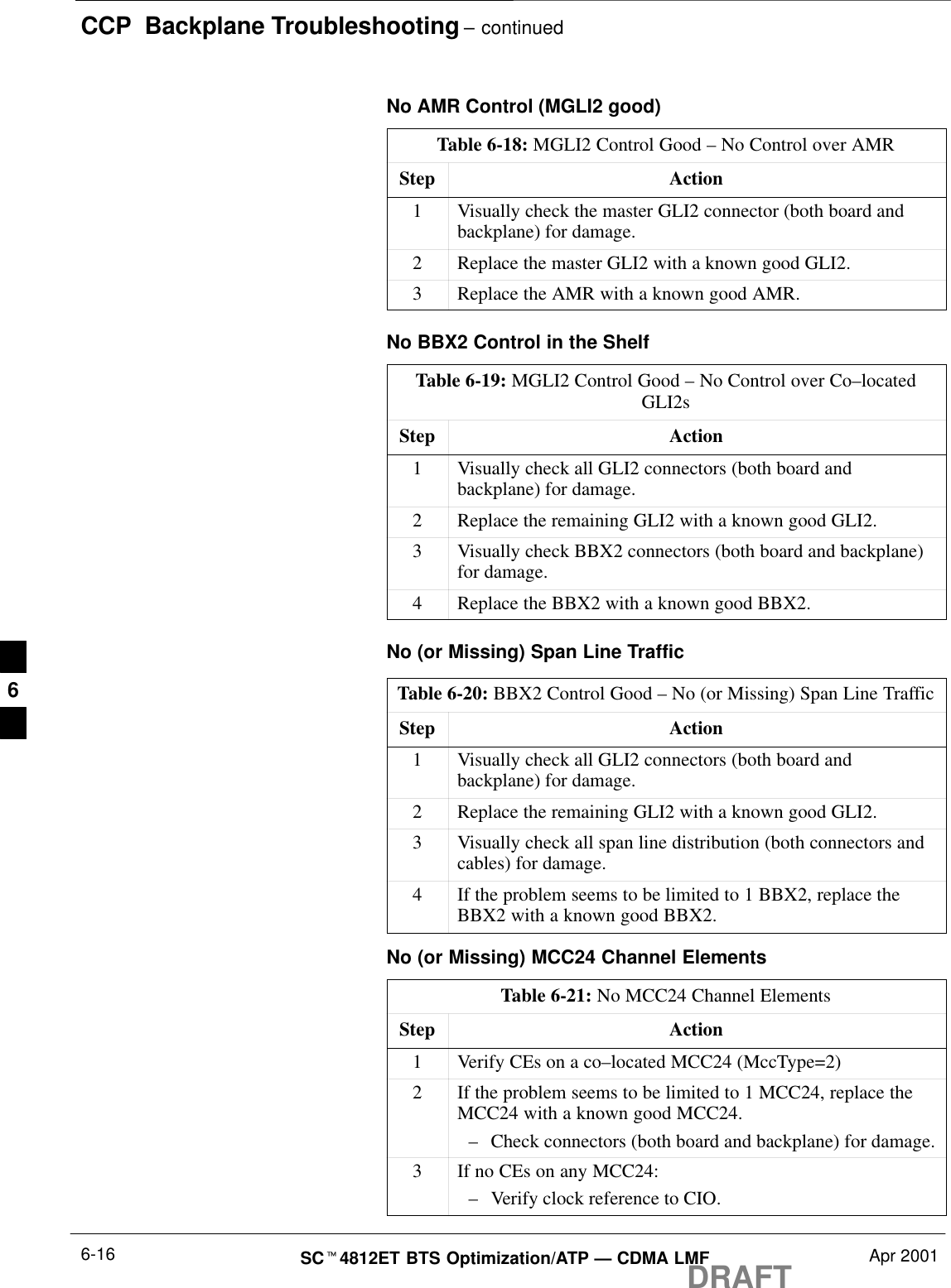
CCP  Backplane Troubleshooting – continuedDRAFTSCt4812ET BTS Optimization/ATP — CDMA LMF Apr 20016-14GLI2 Ethernet “A” and “B” ConnectionsThese BNC connectors are located on the C–CCP backplane and routedto the GLI2 board.  This interface provides all the control and datacommunications between the master GLI2 and the other GLI2, betweengateways, and for the LMF on the LAN.BBX2 ConnectorEach BBX2 connector consists of a Harting 2SU/1SU digital connectorand two 6–conductor coaxial connectors.  These connectors provide DC,digital, and RF inputs/outputs for the BBX2s in the C–CCP backplane.CIO ConnectorsSRX RF antenna path signal inputs are routed through RX Tri–Filters(on the I/O plate), and via coaxial cables to the two MPC modules –the six “A” (main) signals go to one MPC; the six “B” (diversity) tothe other.  The MPC outputs the low–noise–amplified signals via theC–CCP backplane to the CIO where the signals are split and sent tothe appropriate BBX2.SA digital bus then routes the baseband signal through the BBX2, tothe backplane, then on to the MCC24 slots.SDigital TX antenna path signals originate at the MCC24s. Eachoutput is routed from the MCC24 slot via the backplane appropriateBBX2.STX RF path signal originates from the BBX2, through the backplaneto the CIO, through the CIO, and via multi-conductor coaxial cablingto the LPAs in the LPA shelf.C–CCP BackplaneTroubleshooting ProcedureThe following table provides a standard procedure for troubleshootingproblems that appear to be related to a defective C–CCP backplane. Thetable is broken down into possible problems and steps which should betaken in an attempt to find the root cause.It is important to note that all steps be followed beforereplacing ANY C–CCP backplane.IMPORTANT*6
CCP Backplane Troubleshooting – continuedApr 2001 6-15SCt4812ET BTS Optimization/ATP — CDMA LMFDRAFTDigital Control ProblemsNo GLI2 Control via LMF (all GLI2s)Table 6-15: No GLI2 Control via LMF (all GLI2s)Step Action1Check the ethernet for proper connection, damage, shorts, oropens.2Verify C–CCP backplane Shelf ID DIP switch is set correctly.3Visually check the master GLI2 connector (both board andbackplane) for damage.4Replace the master GLI2 with a known good GLI2.No GLI2 Control through Span Line Connection (All GLI2s)Table 6-16: No GLI2 Control through Span Line Connection (BothGLI2s)Step Action1Verify C–CCP backplane Shelf ID DIP switch is set correctly.2Verify that the BTS and GLI2s are correctly configured in theOMCR/CBSC data base.3Visually check the master GLI2 connector (both board andbackplane) for damage.4Replace the master GLI2 with a known good GLI2.5Check the span line inputs from the top of the frame to themaster GLI2 for proper connection and damage.Table 6-17: MGLI2 Control Good – No Control over Co–locatedGLI2Step Action1Verify that the BTS and GLI2s are correctly configured in theOMCR CBSC data base.2Check the ethernet for proper connection, damage, shorts, oropens.3Visually check all GLI2 connectors (both board andbackplane) for damage.4Replace the remaining GLI2 with a known good GLI2. 6
CCP  Backplane Troubleshooting – continuedDRAFTSCt4812ET BTS Optimization/ATP — CDMA LMF Apr 20016-16No AMR Control (MGLI2 good)Table 6-18: MGLI2 Control Good – No Control over AMRStep Action1Visually check the master GLI2 connector (both board andbackplane) for damage.2Replace the master GLI2 with a known good GLI2.3Replace the AMR with a known good AMR.No BBX2 Control in the ShelfTable 6-19: MGLI2 Control Good – No Control over Co–locatedGLI2sStep Action1Visually check all GLI2 connectors (both board andbackplane) for damage.2Replace the remaining GLI2 with a known good GLI2.3Visually check BBX2 connectors (both board and backplane)for damage.4Replace the BBX2 with a known good BBX2.No (or Missing) Span Line TrafficTable 6-20: BBX2 Control Good – No (or Missing) Span Line TrafficStep Action1Visually check all GLI2 connectors (both board andbackplane) for damage.2Replace the remaining GLI2 with a known good GLI2.3Visually check all span line distribution (both connectors andcables) for damage.4If the problem seems to be limited to 1 BBX2, replace theBBX2 with a known good BBX2.No (or Missing) MCC24 Channel ElementsTable 6-21: No MCC24 Channel ElementsStep Action1Verify CEs on a co–located MCC24 (MccType=2)2If the problem seems to be limited to 1 MCC24, replace theMCC24 with a known good MCC24.–Check connectors (both board and backplane) for damage.3If no CEs on any MCC24:–Verify clock reference to CIO.6
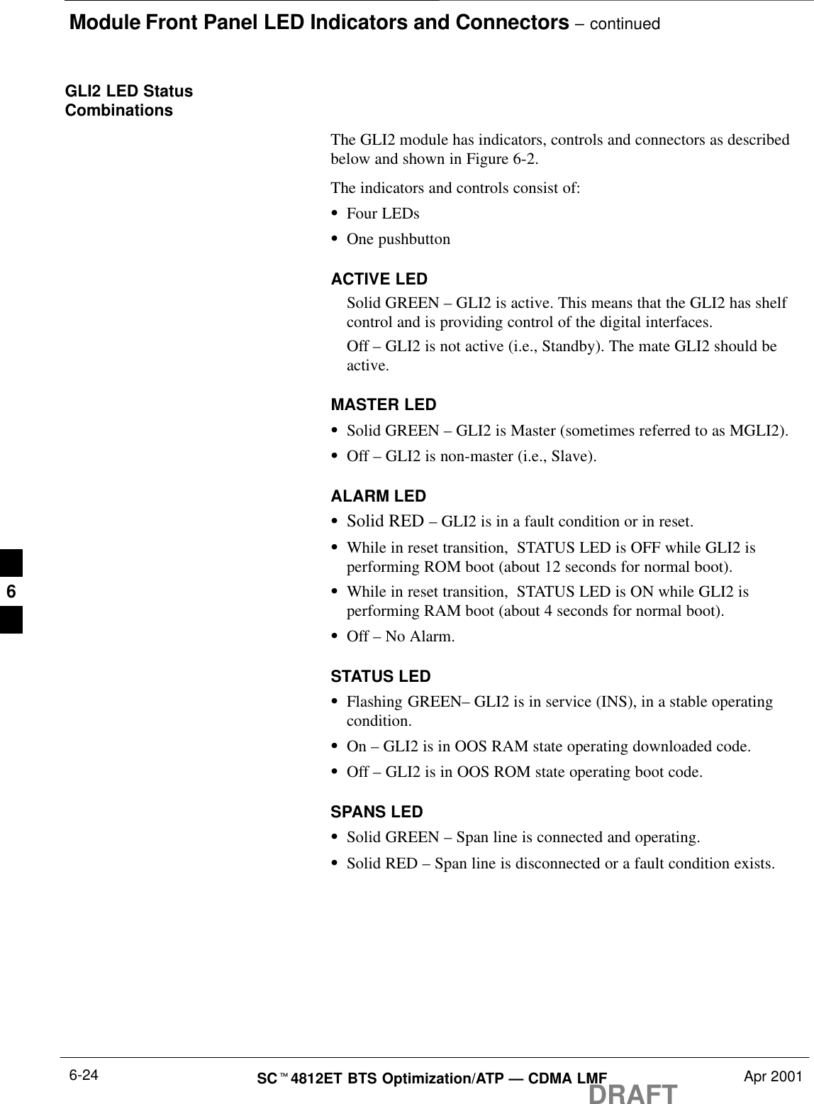
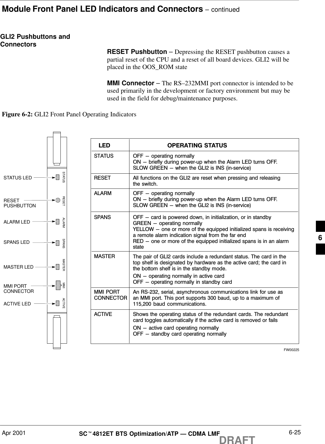
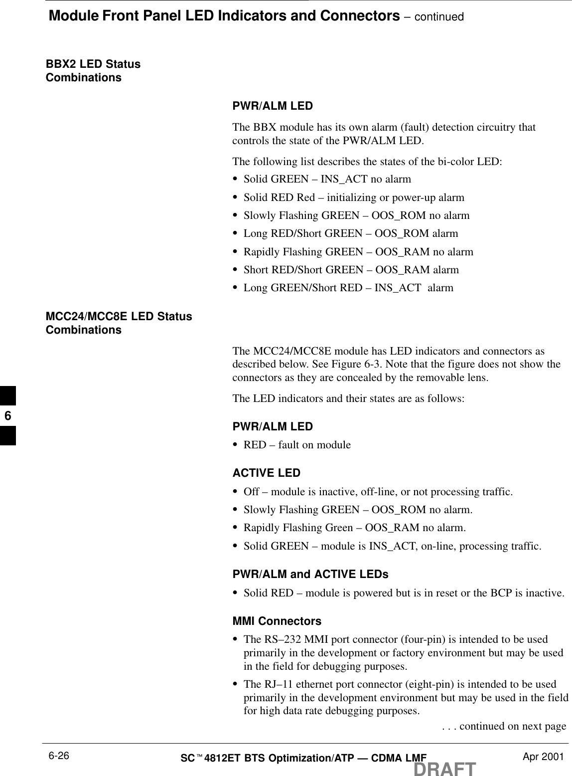
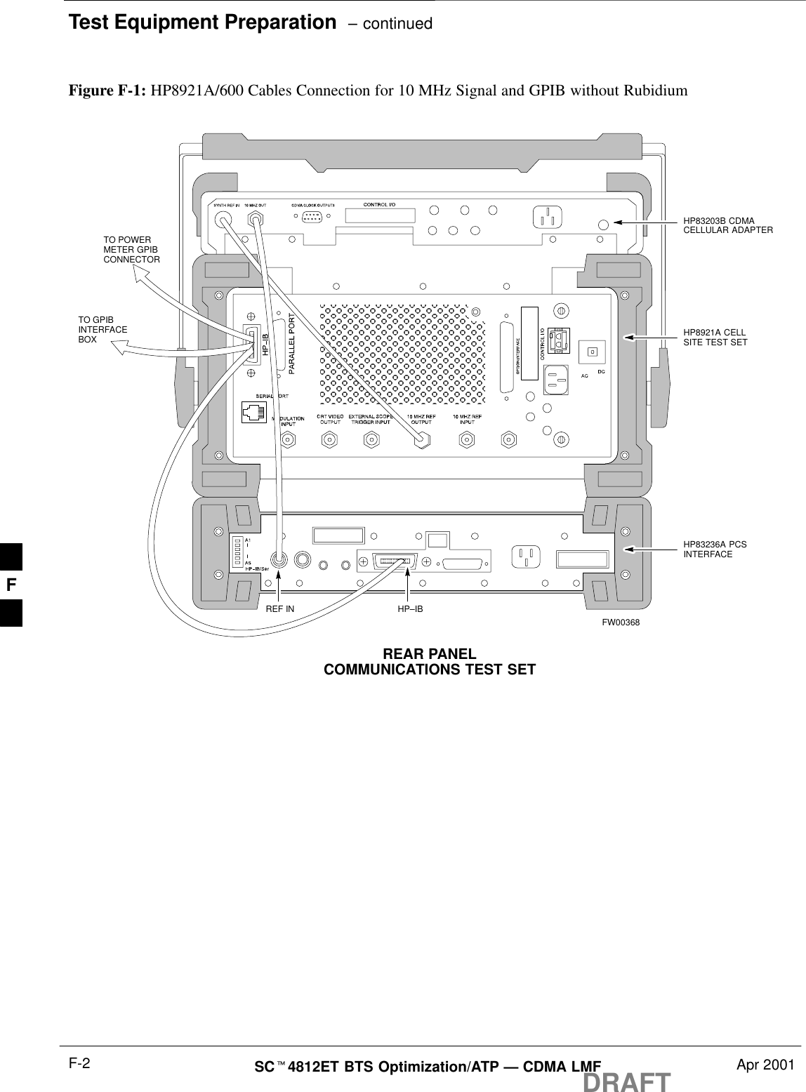
CCP Backplane Troubleshooting – continuedApr 2001 6-17SCt4812ET BTS Optimization/ATP — CDMA LMFDRAFTDC Power ProblemsPotentially lethal voltage and current levels are routed tothe BTS equipment. This test must be carried out with asecond person present, acting in a safety role. Remove allrings, jewelry, and wrist watches prior to beginning thistest.WARNINGNo DC Input Voltage to  Power Supply ModuleTable 6-22: No DC Input Voltage to Power Supply ModuleStep Action1Verify DC power is applied to the BTS frame. Verify there areno breakers tripped.* IMPORTANTIf a breaker has tripped, remove all modules from theapplicable shelf supplied by the breaker and attempt to reset it.–If breaker trips again, there is probably a cable or breakerproblem within the frame.–If breaker does not trip, there is probably a defectivemodule or sub–assembly within the shelf.2Verify that the C–CCP shelf breaker on the BTS framebreaker panel is functional.3Use a voltmeter to determine if the input voltage is beingrouted to the C–CCP backplane by measuring the DC voltagelevel on the PWR_IN cable.–If the voltage is not present, there is probably a cable orbreaker problem within the frame.–If the voltage is present at the connector, reconnect andmeasure the level at the “VCC” power feed clip on thedistribution backplane.  If the voltage is correct at thepower clip, inspect the clip for damage.4If everything appears to be correct, visually inspect the powersupply module connectors.5Replace the power supply module with a known goodmodule.6If steps 1 through 4 fail to indicate a problem, the C–CCPbackplane failure (possibly an open trace) has occurred.6
CCP  Backplane Troubleshooting – continuedDRAFTSCt4812ET BTS Optimization/ATP — CDMA LMF Apr 20016-18No DC Voltage (+5, +6.5, or +15 Volts) to a Specific GLI2,BBX2, or SwitchboardTable 6-23: No DC Input Voltage to any C–CCP Shelf ModuleStep Action1Verify steps outlined in Table 6-22 have been performed.2Inspect the defective board/module (both board andbackplane) connector for damage.3Replace suspect board/module with known goodboard/module.TX and RX Signal RoutingProblemsTable 6-24: No DC Input Voltage to any C–CCP Shelf ModuleStep Action1Inspect all Harting Cable connectors and back–planeconnectors for damage in all the affected board slots.2Perform steps outlined in the RF path troubleshootingflowchart in this manual.6
RFDS – Fault IsolationApr 2001 6-19SCt4812ET BTS Optimization/ATP — CDMA LMFDRAFTIntroductionThe RFDS is used to perform Pre–Calibration Verification andPost-Calibration Audits which  limit-check the RFDS-generate andreported receive levels of every path from the RFDS through thedirectional coupler coupled paths. In the event of test failure, refer to thefollowing tables.All tests failTable 6-25: RFDS Fault Isolation – All tests failStep Action1Check the calibration equipment for proper operation by manually setting the signal generator outputattenuator to the lowest output power setting and connecting the output port to the spectrum analyzerrf input port.2Set the signal generator output attenuator to –90 dBm, and switch on the rf output. Verify that thespectrum analyzer can receive the signal, indicate the correct signal strength, (accounting for the cableinsertion loss), and the approximate frequency.3Visually inspect RF cabling. Make sure each directional coupler forward and reflected port connects tothe RFDS antenna select unit on the RFDS.4Check the wiring against the site documentation wiring diagram or the BTS Site Installation manual.5Verify RGLI and TSU have been downloaded.6Check to see that all RFDS boards show green on the front panel indicators. Visually check  (bothboard and backplane) for damage.7Replace any boards that do not show green with known good boards one at a time in the followingorder. Re–test after each is replaced.–RFDS ASU board.–RFDS Transceiver board. All RX and TX paths failIf every receive or transmit path fails, the problem most likely lies withthe rf converter board or the transceiver board. Refer to the followingtable for  fault isolation procedures.Table 6-26: RFDS Fault Isolation – All RX and TX paths failStep Action1Visually check the master RF converter board (both board and backplane) for damage.2Replace the RF converter board with a known good RF converter board.3Visually check RXCVR TSU (both board and backplane) for damage.4Replace the TSU with a known good TSU.6
RFDS – Fault Isolation – continuedDRAFTSCt4812ET BTS Optimization/ATP — CDMA LMF Apr 20016-20All tests fail on a singleantennaIf all path failures are on one antenna port, forward and/or reflected,make the following checks.Table 6-27: RFDS Fault Isolation – All tests fail on single antenna pathStep Action1Visually inspect the site interface cabinet internal cabling to the suspect directional coupler antennaport.2Verify the forward and reflected ports connect to the correct RFDS antenna select unit positions on theRFDS backplane. Refer to the installation manual for details.3Visually check ASU connectors (both board and backplane) for damage.4Replace the ASU with a known good ASU.5Replace the RF cables between the affected directional coupler and RFDS.NOTEExternally route the cable to bypass suspect segment. 6
Module Front Panel LED Indicators and ConnectorsApr 2001 6-21SCt4812ET BTS Optimization/ATP — CDMA LMFDRAFTModule Status IndicatorsEach of the non-passive plug-in modules has a bi-color (green & red)LED status indicator located on the module front panel. The indicator islabeled PWR/ALM. If both colors are turned on, the indicator is yellow.Each plug-in module, except for the fan module, has its own alarm(fault) detection circuitry that controls the state of the PWR/ALM LED.The fan TACH signal of each fan module is monitored by the AMR.Based on the status of this signal the AMR controls the state of thePWR/ALM LED on the fan module.LED Status Combinations forAll Modules (except GLI2,CSM, BBX2, MCC24E, MCC8E)PWR/ALM LEDThe following list describes the states of the module status indicator.SSolid GREEN –  module operating in a normal (fault free) condition.SSolid RED – module is operating in a fault (alarm) condition due toelectrical hardware failure.Note that a fault (alarm) indication may or may not be due to a completemodule failure and normal service may or may not be reduced orinterrupted.DC/DC Converter LED StatusCombinationsThe PWR CNVTR has its own alarm (fault) detection circuitry thatcontrols the state of the PWR/ALM LED.PWR/ALM LEDThe following list describes the states of the bi-color LED.SSolid GREEN –  module operating in a normal (fault free) condition.SSolid RED –  module is operating in a fault (alarm) condition due toelectrical hardware problem.6
Module Front Panel LED Indicators and Connectors – continuedDRAFTSCt4812ET BTS Optimization/ATP — CDMA LMF Apr 20016-22CSM LED StatusCombinations PWR/ALM LEDThe CSMs include on-board alarm detection. Hardware andsoftware/firmware alarms are indicated via the front panel indicators.After the memory tests, the CSM loads OOS–RAM code from the FlashEPROM, if available. If not available, the OOS–ROM code is loadedfrom the Flash EPROM.SSolid GREEN – module is INS_ACT or INS_STBY no alarm.SSolid RED – Initial power up or module is operating in a fault (alarm)condition.SSlowly Flashing GREEN – OOS_ROM no alarm.SLong RED/Short GREEN – OOS_ROM alarm.SRapidly Flashing GREEN – OOS_RAM no alarm or INS_ACT in DUMB mode.SShort RED/Short GREEN – OOS_RAM alarm.SLong GREEN/Short RED – INS_ACT  or INS_STBY alarm.SOff – no DC power  or on-board fuse is open.SSolid YELLOW – After a reset, the CSMs begin to boot. DuringSRAM test and Flash EPROM code check, the LED is yellow. (IfSRAM or Flash EPROM fail, the LED changes to a solid RED andthe CSM attempts to reboot.)PWR/ALMIndicatorFREQMONITORSYNCMONITORFW00303Figure 6-1: CSM Front Panel Indicators & Monitor Ports . . . continued on next page6
Module Front Panel LED Indicators and Connectors – continuedApr 2001 6-23SCt4812ET BTS Optimization/ATP — CDMA LMFDRAFTFREQ Monitor ConnectorA test port provided at the CSM front panel via a BNC receptacle allowsmonitoring of the 19.6608 MHz clock generated by the CSM. Whenboth CSM 1 and CSM 2 are in an in-service (INS) condition, the CSM 2clock signal frequency is the same as that output by CSM 1.The clock is a sine wave signal with a minimum amplitude of +2 dBm(800 mVpp) into a 50 Ω load connected to this port.SYNC Monitor ConnectorA test port provided at the CSM front panel via a BNC receptacle allowsmonitoring of the “Even Second Tick” reference signal generated by theCSMs.At this port, the reference signal is a TTL active high signal with a pulsewidth of 153 nanoseconds.MMI Connector – Only accessible behind front panel. The RS–232MMI port connector is intended to be used primarily in the developmentor factory environment, but may be used in the field fordebug/maintenance purposes.6
Module Front Panel LED Indicators and Connectors – continuedDRAFTSCt4812ET BTS Optimization/ATP — CDMA LMF Apr 20016-24GLI2 LED StatusCombinationsThe GLI2 module has indicators, controls and connectors as describedbelow and shown in Figure 6-2.The indicators and controls consist of:SFour LEDsSOne pushbuttonACTIVE LEDSolid GREEN – GLI2 is active. This means that the GLI2 has shelfcontrol and is providing control of the digital interfaces.Off – GLI2 is not active (i.e., Standby). The mate GLI2 should beactive.MASTER LEDSSolid GREEN – GLI2 is Master (sometimes referred to as MGLI2).SOff – GLI2 is non-master (i.e., Slave).ALARM LEDSSolid RED – GLI2 is in a fault condition or in reset.SWhile in reset transition,  STATUS LED is OFF while GLI2 isperforming ROM boot (about 12 seconds for normal boot).SWhile in reset transition,  STATUS LED is ON while GLI2 isperforming RAM boot (about 4 seconds for normal boot).SOff – No Alarm.STATUS LEDSFlashing GREEN– GLI2 is in service (INS), in a stable operatingcondition.SOn – GLI2 is in OOS RAM state operating downloaded code.SOff – GLI2 is in OOS ROM state operating boot code.SPANS LEDSSolid GREEN – Span line is connected and operating.SSolid RED – Span line is disconnected or a fault condition exists.6
Module Front Panel LED Indicators and Connectors – continuedApr 2001 6-25SCt4812ET BTS Optimization/ATP — CDMA LMFDRAFTGLI2 Pushbuttons andConnectors RESET Pushbutton – Depressing the RESET pushbutton causes apartial reset of the CPU and a reset of all board devices. GLI2 will beplaced in the OOS_ROM stateMMI Connector – The RS–232MMI port connector is intended to beused primarily in the development or factory environment but may beused in the field for debug/maintenance purposes.MMI PORTCONNECTORACTIVE LEDSTATUS RESET ALARM SPANS MASTER MMI ACTIVESTATUS LEDRESETPUSHBUTTONALARM LEDSPANS LEDMASTER LEDFigure 6-2: GLI2 Front Panel Operating IndicatorsSTATUS OFF - operating normallyON - briefly during powerĆup when the Alarm LED turns OFF.SLOW GREEN - when the GLI2 is INS (inĆservice)RESETALARM OFF - operating normallyON - briefly during powerĆup when the Alarm LED turns OFF.SLOW GREEN - when the GLI2 is INS (inĆservice)SPANSMASTERMMI PORTCONNECTORACTIVELED OPERATING STATUSAll functions on the GLI2 are reset when pressing and releasingthe switch.ON - operating normally in active cardOFF - operating normally in standby cardShows the operating status of the redundant cards. The redundantcard toggles automatically if the active card is removed or failsON - active card operating normallyOFF - standby card operating normallyThe pair of GLI2 cards include a redundant status. The card in thetop shelf is designated by hardware as the active card; the card inthe bottom shelf is in the standby mode.OFF - card is powered down, in initialization, or in standbyGREEN - operating normallyYELLOW - one or more of the equipped initialized spans is receivinga remote alarm indication signal from the far endRED - one or more of the equipped initialized spans is in an alarmstateAn RSĆ232, serial, asynchronous communications link for use asan MMI port. This port supports 300 baud, up to a maximum of115,200  baud communications.FW002256
Module Front Panel LED Indicators and Connectors – continuedDRAFTSCt4812ET BTS Optimization/ATP — CDMA LMF Apr 20016-26BBX2 LED StatusCombinationsPWR/ALM LEDThe BBX module has its own alarm (fault) detection circuitry thatcontrols the state of the PWR/ALM LED.The following list describes the states of the bi-color LED:SSolid GREEN – INS_ACT no alarmSSolid RED Red – initializing or power-up alarmSSlowly Flashing GREEN – OOS_ROM no alarmSLong RED/Short GREEN – OOS_ROM alarmSRapidly Flashing GREEN – OOS_RAM no alarmSShort RED/Short GREEN – OOS_RAM alarmSLong GREEN/Short RED – INS_ACT  alarmMCC24/MCC8E LED StatusCombinationsThe MCC24/MCC8E module has LED indicators and connectors asdescribed below. See Figure 6-3. Note that the figure does not show theconnectors as they are concealed by the removable lens.The LED indicators and their states are as follows:PWR/ALM LEDSRED – fault on moduleACTIVE LEDSOff – module is inactive, off-line, or not processing traffic.SSlowly Flashing GREEN – OOS_ROM no alarm.SRapidly Flashing Green – OOS_RAM no alarm.SSolid GREEN – module is INS_ACT, on-line, processing traffic.PWR/ALM and ACTIVE LEDsSSolid RED – module is powered but is in reset or the BCP is inactive.MMI ConnectorsSThe RS–232 MMI port connector (four-pin) is intended to be usedprimarily in the development or factory environment but may be usedin the field for debugging purposes.SThe RJ–11 ethernet port connector (eight-pin) is intended to be usedprimarily in the development environment but may be used in the fieldfor high data rate debugging purposes. . . . continued on next page6
Module Front Panel LED Indicators and Connectors – continuedApr 2001 6-27SCt4812ET BTS Optimization/ATP — CDMA LMFDRAFTPWR/ALM LEDLENS(REMOVABLE)ACTIVE LEDPWR/ALM ACTIVEFigure 6-3: MCC24/8E Front Panel LEDs and LED IndicatorsPWR/ALM OFF - operating normallyON - briefly during powerĆup and during failureąconditionsACTIVELED OPERATING STATUSRAPIDLY BLINKING - Card is codeĆloaded butąnot  enabledSLOW BLINKING - Card is not codeĆloadedON - card is codeĆloaded and enabledą(INS_ACTIVE)COLORGREENREDRED ON - fault conditionSLOW FLASHING (alternating with green) - CHIąbus inactive on powerĆupAn alarm is generated in the event of a failureFW00224LPA Shelf LED StatusCombinationsLPA Module LEDEach LPA module contains a bi–color LED just above the MMIconnector on the ETIB module. Interpret this LED as follows:SGREEN — LPA module is active and is reporting no alarms (Normalcondition).SFlashing GREEN/RED — LPA module is active but is reporting anlow input power condition. If no BBX is keyed, this is normal anddoes not constitute a failure.SFlashing RED — LPA is in alarm.6
Basic Troubleshooting – Span Control LinkDRAFTSCt4812ET BTS Optimization/ATP — CDMA LMF Apr 20016-28Span Problems(No Control Link)Table 6-28: Troubleshooting Control Link FailurenStep Action1Verify the span settings using the span_view commandon the active master GLI2 MMI port. If these are setcorrectly, verify the edlc parameters using the showcommand. Any alarms conditions indicate that the span isnot operating correctly.–Try looping back the span line from the DSX panelback to the Mobility Manager (MM) and verify thatthe looped signal is good.–Listen for control tone on appropriate timeslot fromBase Site and MM.6
Apr 2001 SCt4812ET BTS Optimization/ATP — CDMA LMFDRAFTAppendix A: Data Sheets Appendix ContentAppendix A: Optimization (Pre–ATP) Data Sheets A-1. . . . . . . . . . . . . . . . . . . . . . Verification of Test Equipment Used A-1. . . . . . . . . . . . . . . . . . . . . . . . . . . Site Checklist A-2. . . . . . . . . . . . . . . . . . . . . . . . . . . . . . . . . . . . . . . . . . . . . Preliminary Operations A-2. . . . . . . . . . . . . . . . . . . . . . . . . . . . . . . . . . . . . Pre–Power and Initial Power  Tests A-3. . . . . . . . . . . . . . . . . . . . . . . . . . . . General Optimization Checklist A-4. . . . . . . . . . . . . . . . . . . . . . . . . . . . . . GPS Receiver Operation A-5. . . . . . . . . . . . . . . . . . . . . . . . . . . . . . . . . . . . LFR Receiver Operation A-6. . . . . . . . . . . . . . . . . . . . . . . . . . . . . . . . . . . . TX Bay Level Offset / Power Output Verification for    3–Sector Configurations A-7. . . . . . . . . . . . . . . . . . . . . . . . . . . . . . . . . . TX Bay Level Offset / Power Output Verification for    6–Sector Configurations A-12. . . . . . . . . . . . . . . . . . . . . . . . . . . . . . . . . . BTS Redundancy/Alarm Tests A-14. . . . . . . . . . . . . . . . . . . . . . . . . . . . . . . TX Antenna VSWR A-14. . . . . . . . . . . . . . . . . . . . . . . . . . . . . . . . . . . . . . . . RX Antenna VSWR A-15. . . . . . . . . . . . . . . . . . . . . . . . . . . . . . . . . . . . . . . . AMR Verification A-15. . . . . . . . . . . . . . . . . . . . . . . . . . . . . . . . . . . . . . . . . Appendix A: Site Serial Number Check List A-16. . . . . . . . . . . . . . . . . . . . . . . . . . . C–CCP Shelf A-16. . . . . . . . . . . . . . . . . . . . . . . . . . . . . . . . . . . . . . . . . . . . . LPAs A-17. . . . . . . . . . . . . . . . . . . . . . . . . . . . . . . . . . . . . . . . . . . . . . . . . . . . A
Table of Contents  – continuedDRAFTSCt4812ET BTS Optimization/ATP — CDMA LMF Apr 2001NotesA
Appendix A: Optimization (Pre–ATP) Data SheetsApr 2001 A-1SCt4812ET BTS Optimization/ATP — CDMA LMFDRAFTVerification of Test EquipmentUsedTable A-1: Verification of Test Equipment UsedManufacturer Model Serial NumberComments:__________________________________________________________________________________________________________________________A
Appendix A: Optimization (Pre–ATP) Data Sheets – continuedDRAFTSCt4812ET BTS Optimization/ATP — CDMA LMF Apr 2001A-2Site ChecklistTable A-2: Site ChecklistOK Parameter Specification Comments-Deliveries Per established procedures-Floor Plan Verified---Inter Frame Cables:EthernetFrame GroundPowerPer procedurePer procedurePer procedure---Factory Data:BBX2Test PanelRFDSPer procedurePer procedurePer procedure-Site Temperature-Dress Covers/BracketsPreliminary OperationsTable A-3: Preliminary OperationsOK Parameter Specification Comments-Shelf ID Dip Switches Per site equipage-Ethernet LAN verification Verified per procedureComments:_________________________________________________________A
Appendix A: Optimization (Pre–ATP) Data Sheets – continuedApr 2001 A-3SCt4812ET BTS Optimization/ATP — CDMA LMFDRAFTPre–Power and Initial PowerTestsTable A3a: Pre–power ChecklistOK Parameter Specification Comments-Pre–power–up tests Verify power supplyoutput voltage at the topof each BTS frame iswithin specifications--------Internal Cables:ISB (all cages)CSM (all cages)Power (all cages)Ethernet ConnectorsLAN A ohmsLAN B ohmsLAN A shieldLAN B shieldEthernet Bootsverifiedverifiedverifiedverifiedverifiedisolatedisolatedinstalled-Air Impedance Cage (single cage) installed-Initial power–up tests Verify power supplyoutput voltage at the topof each BTS frame iswithin specifications:Comments:_________________________________________________________A
Appendix A: Optimization (Pre–ATP) Data Sheets – continuedDRAFTSCt4812ET BTS Optimization/ATP — CDMA LMF Apr 2001A-4General OptimizationChecklistTable A3b: Pre–power ChecklistOK Parameter Specification Comments--LEDsFrame fansilluminatedoperational----LMF to BTS ConnectionPreparing the LMFLog into the LMF PCCreate site specific BTS directoryDownload device loadsper procedureper procedureper procedureper procedure--Ping LAN APing LAN Bper procedureper procedure---------Download/Enable MGLI2sDownload/Enable GLI2sSet Site Span ConfigurationDownload CSMsEnable CSMsEnable CSMsDownload/Enable MCCs*Download BBXs*Download TSU  (in RFDS)Program TSU NAMper procedureper procedureper procedureper procedureper procedureper procedureper procedureper procedureper procedure-Test Set Calibration per procedure*MCCs may be MCC8Es, MCC24s or MCC–1Xs. BBXs may be BBX2s or BBX1XsComments:_________________________________________________________A
Appendix A: Optimization (Pre–ATP) Data Sheets – continuedApr 2001 A-5SCt4812ET BTS Optimization/ATP — CDMA LMFDRAFTGPS Receiver OperationTable A-4: GPS Receiver OperationOK Parameter Specification Comments-GPS Receiver Control Task State:tracking satellitesVerify parameter-Initial Position Accuracy: Verify Estimatedor Surveyed-Current Position:latlonheightRECORD inmsec and cm alsoconvert to degmin sec-Current Position: satellites trackedEstimated:(>4) satellites tracked,(>4) satellites visibleSurveyed:(>1) satellite tracked,(>4) satellites visibleVerify parameteras appropriate:-GPS Receiver Status:Current Dilution ofPrecision (PDOP or HDOP): (<30)Verify parameter-Current reference source:Number: 0; Status: Good; Valid: Yes Verify parameterComments:_________________________________________________________A
Appendix A: Optimization (Pre–ATP) Data Sheets – continuedDRAFTSCt4812ET BTS Optimization/ATP — CDMA LMF Apr 2001A-6LFR Receiver OperationTable A-5: LFR Receiver OperationOK Parameter Specification Comments-Station call letters M X Y Zassignment. as specified in sitedocumentation-SN ratio is > 8 dB-LFR Task State: 1frlocked to station xxxxVerify parameter-Current reference source:Number: 1; Status: Good; Valid: YesVerify parameterComments:_________________________________________________________A
Appendix A: Optimization (Pre–ATP) Data Sheets – continuedApr 2001 A-7SCt4812ET BTS Optimization/ATP — CDMA LMFDRAFTLPA IM Reduction Table A-6: LPA IM ReductionParameter CommentsCARRIEROK LPA#4:1 & 2:13–Sector 2:16–Sector Dual BP3–Sector Dual BP6–SectorSpecification-1A C1 C1 C1 C1 No Alarms-1B C1 C1 C1 C1 No Alarms-1C C1 C1 C1 C1 No Alarms-1D C1 C1 C1 C1 No Alarms-2A C2 C2 C2 No Alarms-2B C2 C2 C2 No Alarms-2C C2 C2 C2 No Alarms-2D C2 C2 C2 No Alarms-3A C3 C1 C1 No Alarms-3B C3 C1 C1 No Alarms-3C C3 C1 C1 No Alarms-3D C3 C1 C1 No Alarms-4A C4 C2 No Alarms-4B C4 C2 No Alarms-4C C4 C2 No Alarms-4D C4 C2 No AlarmsComments:_________________________________________________________A
Appendix A: Optimization (Pre–ATP) Data Sheets – continuedDRAFTSCt4812ET BTS Optimization/ATP — CDMA LMF Apr 2001A-8TX Bay Level Offset / PowerOutput Verification for3–Sector Configurations  1–Carrier2–Carrier Non–adjacent Channels4–Carrier Non–adjacent ChannelsTable A-7: TX BLO Calibration (3–Sector: 1–Carrier,  2–Carrier and 4–Carrier Non–adjacent Channels)OK Parameter Specification Comments-BBX2–1, ANT–1 =  dBBBX2–r, ANT–1 =  dB-Calibratecarrier 1 TX Bay Level Offset = 37 dB (+4 dB)prior to calibrationBBX2–2, ANT–2 =  dBBBX2–r, ANT–2 =  dB-BBX2–3, ANT–3 =  dBBBX2–r, ANT–3 =  dB-BBX2–7, ANT–1 =  dBBBX2–r, ANT–1 =  dB-Calibratecarrier 2 TX Bay Level Offset = 37 dB (+4 dB)prior to calibrationBBX2–8, ANT–2 =  dBBBX2–r, ANT–2 =  dB-BBX2–9, ANT–3 =  dBBBX2–r, ANT–3 =  dB-BBX2–4, ANT–1 =  dBBBX2–r, ANT–1 =  dB-Calibratecarrier 3 TX Bay Level Offset = 37 dB (+4 dB)prior to calibrationBBX2–5, ANT–2 =  dBBBX2–r, ANT–2 =  dB-BBX2–6, ANT–3 =  dBBBX2–r, ANT–3 =  dB-BBX2–10, ANT–1 =  dBBBX2–r, ANT–1 =  dB-Calibratecarrier 4 TX Bay Level Offset = 37 dB (+4 dB)prior to calibrationBBX2–11, ANT–2 =  dBBBX2–r, ANT–2 =  dB-BBX2–12, ANT–3 =  dBBBX2–r, ANT–3 =  dB. . . continued on next pageA
Appendix A: Optimization (Pre–ATP) Data Sheets – continuedApr 2001 A-9SCt4812ET BTS Optimization/ATP — CDMA LMFDRAFTTable A-7: TX BLO Calibration (3–Sector: 1–Carrier,  2–Carrier and 4–Carrier Non–adjacent Channels)OK CommentsSpecificationParameter-BBX2–1, ANT–1 =  dBBBX2–r, ANT–1 =  dB-CalibrationAuditcarrier 10 dB (+0.5 dB) for gain set resolutionpost calibrationBBX2–2, ANT–2 =  dBBBX2–r, ANT–2 =  dB-carrier 1BBX2–3, ANT–3 =  dBBBX2–r, ANT–3 =  dB-BBX2–7, ANT–1 =  dBBBX2–r, ANT–1 =  dB-CalibrationAuditcarrier 20 dB (+0.5 dB) for gain set resolutionpost calibrationBBX2–8, ANT–2 =  dBBBX2–r, ANT–2 =  dB-carrier 2BBX2–9, ANT–3 =  dBBBX2–r, ANT–3 =  dB-BBX2–4, ANT–1 =  dBBBX2–r, ANT–1 =  dB-CalibrationAuditcarrier 30 dB (+0.5 dB) for gain set resolutionpost calibrationBBX2–5, ANT–2 =  dBBBX2–r, ANT–2 =  dB-carrier 3BBX2–6, ANT–3 =  dBBBX2–r, ANT–3 =  dB-BBX2–10, ANT–1 =  dBBBX2–r, ANT–1 =  dB-CalibrationAuditcarrier 40 dB (+0.5 dB) for gain set resolutionpost calibrationBBX2–11, ANT–2 =  dBBBX2–r, ANT–2 =  dB-carrier 4BBX2–12, ANT–3 =  dBBBX2–r, ANT–3 =  dB Comments:__________________________________________________________________________________________________________________________A
Appendix A: Optimization (Pre–ATP) Data Sheets – continuedDRAFTSCt4812ET BTS Optimization/ATP — CDMA LMF Apr 2001A-102–Carrier Adjacent ChannelTable A-8: TX Bay Level Offset Calibration (3–Sector: 2–Carrier Adjacent Channels)OK Parameter Specification Comments-BBX2–1, ANT–1 =  dBBBX2–r, ANT–1 =  dB-Calibratecarrier 1 TX Bay Level Offset = 42 dB (typical),38 dB (minimum) prior to calibrationBBX2–2, ANT–2 =  dBBBX2–r, ANT–2 =  dB-BBX2–3, ANT–3 =  dBBBX2–r, ANT–3 =  dB-BBX2–7, ANT–4 =  dBBBX2–r, ANT–4 =  dB-Calibratecarrier 2 TX Bay Level Offset = 42 dB (typical),38 dB (minimum) prior to calibrationBBX2–8, ANT–5 =  dBBBX2–r, ANT–5 =  dB-BBX2–9, ANT–6 =  dBBBX2–r, ANT–6 =  dB-BBX2–1, ANT–1 =  dBBBX2–r, ANT–1 =  dB-CalibrationAuditcarrier 10 dB (+0.5 dB) for gain set resolutionpost calibrationBBX2–2, ANT–2 =  dBBBX2–r, ANT–2 =  dB-carrier 1BBX2–3, ANT–3 =  dBBBX2–r, ANT–3 =  dB-BBX2–7, ANT–4 =  dBBBX2–r, ANT–4 =  dB-CalibrationAuditcarrier 20 dB (+0.5 dB) for gain set resolutionpost calibrationBBX2–8, ANT–5 =  dBBBX2–r, ANT–5 =  dB-carrier 2BBX2–9, ANT–6 =  dBBBX2–r, ANT–6 =  dB Comments:__________________________________________________________________________________________________________________________A
Appendix A: Optimization (Pre–ATP) Data Sheets – continuedApr 2001 A-11SCt4812ET BTS Optimization/ATP — CDMA LMFDRAFT3–Carrier Adjacent Channels4–Carrier Adjacent ChannelsTable A-9: TX Bay Level Offset Calibration (3–Sector: 3 or 4–Carrier Adjacent Channels)OK Parameter Specification Comments-BBX2–1, ANT–1 =  dBBBX2–r, ANT–1 =  dB-Calibratecarrier 1 TX Bay Level Offset = 37 dB beforecalibrationBBX2–2, ANT–2 =  dBBBX2–r, ANT–2 =  dB-BBX2–3, ANT–3 =  dBBBX2–r, ANT–3 =  dB-BBX2–7, ANT–1 =  dBBBX2–r, ANT–1 =  dB-Calibratecarrier 2 TX Bay Level Offset =37 dB beforecalibrationBBX2–8, ANT–2 =  dBBBX2–r, ANT–2 =  dB-BBX2–9, ANT–3 =  dBBBX2–r, ANT–3 =  dB-BBX2–4, ANT–4 =  dBBBX2–r, ANT–4 =  dB-Calibratecarrier 3 TX Bay Level Offset = 37 dB beforecalibrationBBX2–5, ANT–5 =  dBBBX2–r, ANT–5 =  dB-BBX2–6, ANT–6 =  dBBBX2–r, ANT–6 =  dB-BBX2–10, ANT–4 =  dBBBX2–3, ANT–4 =  dB-Calibratecarrier 4 TX Bay Level Offset = 37 dB beforecalibrationBBX2–11, ANT–5 =  dBBBX2–r, ANT–5 =  dB-BBX2–12, ANT–6 =  dBBBX2–r, ANT–6 =  dB-BBX2–1, ANT–1 =  dBBBX2–r, ANT–1 =  dB-CalibrationAuditcarrier 10 dB (+0.5 dB) for gain set resolutionpost calibrationBBX2–2, ANT–2 =  dBBBX2–r, ANT–2 =  dB-carrier 1BBX2–3, ANT–3 =  dBBBX2–r, ANT–3 =  dB. . . continued on next pageA
Appendix A: Optimization (Pre–ATP) Data Sheets – continuedDRAFTSCt4812ET BTS Optimization/ATP — CDMA LMF Apr 2001A-12Table A-9: TX Bay Level Offset Calibration (3–Sector: 3 or 4–Carrier Adjacent Channels)OK CommentsSpecificationParameter-BBX2–7, ANT–1 =  dBBBX2–r, ANT–1 =  dB-CalibrationAuditcarrier 20 dB (+0.5 dB) for gain set resolutionpost calibrationBBX2–8, ANT–2 =  dBBBX2–r, ANT–2 =  dB-carrier 2BBX2–9, ANT–3 =  dBBBX2–r, ANT–3 =  dB-BBX2–4, ANT–4 =  dBBBX2–r, ANT–4 =  dB-CalibrationAuditcarrier 30 dB (+0.5 dB) for gain set resolutionpost calibrationBBX2–5, ANT–5 =  dBBBX2–r, ANT–5 =  dB-carrier 3BBX2–6, ANT–6 =  dBBBX2–r, ANT–6 =  dB-BBX2–10, ANT–4 =  dBBBX2–r, ANT–4 =  dB-CalibrationAuditcarrier 40 dB (+0.5 dB) for gain set resolutionpost calibrationBBX2–11, ANT–5 =  dBBBX2–r, ANT–5 =  dB-carrier 4BBX2–12, ANT–6 =  dBBBX2–r, ANT–6 =  dB Comments:__________________________________________________________________________________________________________________________A
Appendix A: Optimization (Pre–ATP) Data Sheets – continuedApr 2001 A-13SCt4812ET BTS Optimization/ATP — CDMA LMFDRAFTTX Bay Level Offset / PowerOutput Verification for6–Sector Configurations  1–Carrier2–Carrier Non–adjacent ChannelsTable A-10: TX BLO Calibration (6–Sector: 1–Carrier, 2–Carrier Non–adjacent Channels)OK Parameter Specification Comments-BBX2–1, ANT–1 =  dBBBX2–r, ANT–1 =  dB-BBX2–2, ANT–2 =  dBBBX2–r, ANT–2 =  dB-Calibrate TX Bay Level Offset = 42 dB (typical),BBX2–3, ANT–3 =  dBBBX2–r, ANT–3 =  dB-carrier 1 38 dB (minimum) prior to calibration BBX2–4, ANT–4 =  dBBBX2–r, ANT–4 =  dB-BBX2–5, ANT–5 =  dBBBX2–r, ANT–5 =  dB-BBX2–6, ANT–6 =  dBBBX2–r, ANT–6 =  dB-BBX2–7, ANT–1 =  dBBBX2–r, ANT–1 =  dB-BBX2–8, ANT–2 =  dBBBX2–r, ANT–2 =  dB-Calibrate TX Bay Level Offset = 42 dB (typical),BBX2–9, ANT–3 =  dBBBX2–r, ANT–3 =  dB-carrier 2 38 dB (minimum) prior to calibration BBX2–10, ANT–4 =  dBBBX2–3, ANT–4 =  dB-BBX2–11, ANT–5 =  dBBBX2–r, ANT–5 =  dB-BBX2–12, ANT–6 =  dBBBX2–r, ANT–5 =  dB. . . continued on next pageA
Appendix A: Optimization (Pre–ATP) Data Sheets – continuedDRAFTSCt4812ET BTS Optimization/ATP — CDMA LMF Apr 2001A-14Table A-10: TX BLO Calibration (6–Sector: 1–Carrier, 2–Carrier Non–adjacent Channels)OK CommentsSpecificationParameter-BBX2–1, ANT–1 =  dBBBX2–r, ANT–1 =  dB-BBX2–2, ANT–2 =  dBBBX2–r, ANT–2 =  dB-Calibration 0 dB (+0.5 dB) for gain set resolutionBBX2–3, ANT–3 =  dBBBX2–r, ANT–3 =  dB-Auditcarrier 1 post calibration BBX2–4, ANT–4 =  dBBBX2–r, ANT–4 =  dB-BBX2–5, ANT–5 =  dBBBX2–r, ANT–5 =  dB-BBX2–6, ANT–6 =  dBBBX2–r, ANT–6 =  dB-BBX2–7, ANT–1 =  dBBBX2–r, ANT–1 =  dB-BBX2–8, ANT–2 =  dBBBX2–r, ANT–2 =  dB-Calibration 0 dB (+0.5 dB) for gain set resolutionBBX2–9, ANT–3 =  dBBBX2–r, ANT–3 =  dB-Auditcarrier 2 post calibration BBX2–10, ANT–4 =  dBBBX2–r, ANT–4 =  dB-BBX2–11, ANT–5 =  dBBBX2–r, ANT–5 =  dB-BBX2–12, ANT–6 =  dBBBX2–r, ANT–6 =  dB Comments:__________________________________________________________________________________________________________________________A
Appendix A: Optimization (Pre–ATP) Data Sheets – continuedApr 2001 A-15SCt4812ET BTS Optimization/ATP — CDMA LMFDRAFTTX Antenna VSWRTable A-11: TX Antenna VSWROK Parameter Specification Data-VSWR – Antenna 1    < (1.5 : 1)-VSWR –Antenna 2    < (1.5 : 1)-VSWR –Antenna 3    < (1.5 : 1)-VSWR –Antenna 4    < (1.5 : 1)-VSWR –Antenna 5    < (1.5 : 1)-VSWR –Antenna 6    < (1.5 : 1)Comments:__________________________________________________________________________________________________________________________A
Appendix A: Optimization (Pre–ATP) Data Sheets – continuedDRAFTSCt4812ET BTS Optimization/ATP — CDMA LMF Apr 2001A-16RX Antenna VSWRTable A-12: RX Antenna VSWROK Parameter Specification Data-VSWR – Antenna 1    < (1.5 : 1)-VSWR –Antenna 2    < (1.5 : 1)-VSWR –Antenna 3    < (1.5 : 1)-VSWR –Antenna 4    < (1.5 : 1)-VSWR –Antenna 5    < (1.5 : 1)-VSWR –Antenna 6    < (1.5 : 1)Comments:_________________________________________________________Alarm VerificationTable A-13: CDI Alarm Input VerificationOK Parameter Specification Data-Verify CDI alarm inputoperation per Table 3-1. BTS Relay #XX –Contact AlarmSets/ClearsComments:_________________________________________________________A
Appendix A: Site Serial Number Check ListApr 2001 A-17SCt4812ET BTS Optimization/ATP — CDMA LMFDRAFTDate SiteC–CCP ShelfSite I/O A & BC–CCP ShelfCSM–1CSM–2HSOCCD–1CCD–2AMR–1AMR–2MPC–1MPC–2Fans 1–3 GLI2–1GLI2–2BBX2–1BBX2–2BBX2–3BBX2–4BBX2–5BBX2–6BBX2–7BBX2–8BBX2–9BBX2–10BBX2–11BBX2–12BBX2–rMCC24/MCC8E–1MCC24/MCC8E–2MCC24/MCC8E–3MCC24/MCC8E–4MCC24/MCC8E–5MCC24/MCC8E–6MCC24/MCC8E–7MCC24/MCC8E–8MCC24/MCC8E–9MCC24/MCC8E–10MCC24/MCC8E–11A
Appendix A: Site Serial Number Check List – continuedDRAFTSCt4812ET BTS Optimization/ATP — CDMA LMF Apr 2001A-18MCC24/MCC8E–12CIOSWITCHPS–1PS–2PS–3LPAsLPA 1ALPA 1BLPA 1CLPA 1DLPA 2ALPA 2BLPA 2CLPA 2DLPA 3ALPA 3BLPA 3CLPA 3DLPA 4ALPA 4BLPA 4CLPA 4DA
Apr 2001 SCt4812ET BTS Optimization/ATP — CDMA LMFDRAFTAppendix B: FRU Optimization/ATP Test Matrix Appendix ContentAppendix B: FRU Optimization/ATP Test Matrix B-1. . . . . . . . . . . . . . . . . . . . . . . Usage & Background B-1. . . . . . . . . . . . . . . . . . . . . . . . . . . . . . . . . . . . . . . . . . . . . Detailed Optimization/ATP Test Matrix B-2. . . . . . . . . . . . . . . . . . . . . . . . . . . . . . . B
Table of Contents  – continuedDRAFTSCt4812ET BTS Optimization/ATP — CDMA LMF Apr 2001NotesB
Appendix B: FRU Optimization/ATP Test MatrixApr 2001 B-1SCt4812ET BTS Optimization/ATP — CDMA LMFDRAFTUsage & BackgroundPeriodic maintenance of a site may also may mandate re–optimization ofspecific portions of the site. An outline of some basic guidelines isincluded in the following tables.Re–optimization steps listed for any assembly detailed inthe tables below must be performed anytime a RF cableassociated with it is replaced.IMPORTANT*BTS FrameTable B-1: When RF Optimization Is required on the BTSItem Replaced Optimize:C–CCP Shelf All sector TX and RX paths to allCombined CDMA Channel Processor(C–CCP) shelves.Multicoupler/Preselector Card The three or six affected sector RX paths forthe C–CCP shelf in the BTS frames.Preselector I/O All sector RX paths.BBX2 board RX and TX paths of the affected C–CCPshelf / BBX2 board.CIO Card All RX and TX paths of the affectedCDMA carrier.Any LPA Module The affected sector TX path.LPA Backplane The affected sector TX path.LPA Filter The affected sector TX path.Ancillary Frame Item Replaced Optimize:Directional Coupler All affected sector RX and TX paths to allBTS frame shelves.Site filter All affected RX sector paths in all shelvesin all BTS frames.Any RFDS componentor TSU. The RFDS calibration RX & TX paths(MONFWD/GENFWD). . . . continued on next pageB
Appendix B: FRU Optimization/ATP Test Matrix – continuedDRAFTSCt4812ET BTS Optimization/ATP — CDMA LMF Apr 2001B-2Inter-frame CablingOptimization must be performed after the replacement of any RF cablingbetween BTS frames.Table B-2: When to Optimize Inter–frame CablingItem Replaced Optimize:Ancillary frame to BTSframe (RX) cables The affected sector/antenna RXpaths.BTS frame to ancillary frame(TX) cables The affected sector/antenna TX paths.Detailed Optimization/ATPTest MatrixTable B-3 outlines in more detail the tests that would need to beperformed if one of the BTS components were to fail and be replaced. Itis also assumed that all modules are placed OOS–ROM via the LMFuntil full redundancy of all applicable modules is implemented.The following guidelines should also be noted when using this table.Not every procedure required to bring the site back on lineis indicated in Table B-3. It is meant to be used as aguideline ONLY. The table assumes that the user is familiarenough with the BTS Optimization/ATP procedure tounderstand which test equipment set ups, calibrations, andBTS site preparation will be required before performing theTable # procedures referenced.IMPORTANT*Various passive BTS components (such as the TX and RX directionalcouplers, Preselector IO, CIO; etc.) only call for a TX or RX calibrationaudit to be performed in lieu of a full path calibration. If the RX or TXpath calibration audit fails, the entire RF path calibration will need to berepeated. If the RF path calibration fails, further troubleshooting iswarranted.Whenever any C–CCP BACKPLANE is replaced, it is assumed thatonly power to the C–CCP shelf being replaced is turned off via thebreaker supplying that shelf.Whenever any DISTRIBUTION BACKPLANE is replaced it is assumedthat the power to the entire RFM frame is removed and the PreselectorI/O is replaced. The modem frame should be brought up as if it were anew installation.B
Appendix B: FRU Optimization/ATP Test Matrix – continuedApr 2001 B-3SCt4812ET BTS Optimization/ATP — CDMA LMFDRAFTIf any significant change in signal level results from anycomponent being replaced in the RX or TX signal flowpaths, it would be identified by re–running the RX and TXcalibration audit command.NOTEWhen the CIO is replaced, the C–CCP shelf remains powered up. TheBBX2 boards may need to be removed, then re–installed into theiroriginal slots, and re–downloaded (code and BLO data). RX and TXcalibration audits should then be performed.B
Appendix B: FRU Optimization/ATP Test Matrix – continuedDRAFTSCt4812ET BTS Optimization/ATP — CDMA LMF Apr 2001B-4Table B-3: SC 4812ET BTS Optimization and ATP Test MatrixDocTbl#DescriptionDirectional Coupler (RX)Directional Coupler (TX)RX FilterRX CablesTX CablesMulticoupler/PreselectorCIOC–CCP BackplaneBBX2MCC24/MCC8ECSMLFR/HSOGPSGLI2LPALPA Filter BandpassPower Converters (See Note)SWITCH CARDLPA Combiner Filter 2:1LPA Combiner Filter 4:1LPA BackplaneTable 2-1Initial Boards/ModulesInstall, PreliminaryOperations, CDF SiteEquipage; etc.DDDDDDDDDDDDDDDDDDDDDTable 2-5 Initial Power-up D DTable 3-6/Table 3-8 Start LMF D D D D D DTable 3-13/Table 3-14 Download Code D DTable 3-16 Enable  CSMs D DTable 3-19 GPS Initialization /Verification D D DTable 3-20 LFR  Initialization /Verification D DTable 3-33 TX Path Calibration D D DTable 3-34 Download Offsets to BBX2 D D DTable 3-35 TX Path Calibration Audit D D D D D D D D D D DTable 4–1Spectral Purity TX Mask D D D D D D D DTable 4–1Waveform Quality (rho) D D D D D D D D D DTable 4–1Pilot Time Offset D D D D D D D D D DTable 4–1Code Domain Power /Noise Floor DDDTable 4–1FER Test DDDDDNOTEReplace power converters one card at a time so that power to the C–CCP shelf is not lost. If power to the shelfis lost, all cards in the shelf must be downloaded again.B
Apr 2001 SCt4812ET BTS Optimization/ATP — CDMA LMFDRAFTAppendix C: BBX Gain Set Point vs. BTS Output Considerations Appendix ContentUsage & Background C-1. . . . . . . . . . . . . . . . . . . . . . . . . . . . . . . . . . . . . . . . . . . . . C
Table of Contents  – continuedDRAFTSCt4812ET BTS Optimization/ATP — CDMA LMF Apr 2001NotesC
Appendix C: BBX2 Gain Set Point vs. BTS Output ConsiderationsApr 2001 C-1SCt4812ET BTS Optimization/ATP — CDMA LMFDRAFTUsage & BackgroundTable C-1 outlines the relationship between the total of all code domainchannel element gain settings (digital root sum of the squares) and theBBX2 Gain Set Point  between 33.0 dBm and 44.0 dBm. The resultantRF output (as measured at the top of the BTS in dBm) is shown in thetable.  The table assumes that the BBX2 Bay Level Offset (BLO) valueshave been calculated.As an illustration, consider a  BBX2 keyed up to produce a CDMAcarrier with only the Pilot channel (no MCCs forward link enabled).Pilot gain is set to 262. In this case, the BBX2 Gain Set Point is shownto correlate exactly to the actual RF output anywhere in the 33 to 44dBm output range.  (This is the level used to calibrate the BTS).Table C-1: BBX2 Gain Set Point vs. Actual BTS Output (in dBm)dBm'Gainb44 43 42 41 40 39 38 37 36 35 34 33541 –––––––43.3 42.3 41.3 40.3 39.3533 –––––––43.2 42.2 41.2 40.2 39.2525 –––––––43 42 41 40 39517 –––––––42.9 41.9 40.9 39.9 38.9509 –––––––42.8 41.8 40.8 39.8 38.8501 –––––––42.6 41.6 40.6 39.6 38.6493 – – – – – – 43.5 42.5 41.5 40.5 39.5 38.5485 – – – – – – 43.4 42.4 41.4 40.4 39.4 38.4477 – – – – – – 43.2 42.2 41.2 40.2 39.2 38.2469 – – – – – – 43.1 42.1 41.1 40.1 39.1 38.1461 – – – – – – 42.9 41.9 40.9 39.9 38.9 37.9453 – – – – – – 42.8 41.8 40.8 39.8 38.8 37.8445 –––––43.6 42.6 41.6 40.6 39.6 38.6 37.6437 –––––43.4 42.4 41.4 40.4 39.4 38.4 37.4429 –––––43.3 42.3 41.3 40.3 39.3 38.3 37.3421 –––––43.1 42.1 41.1 40.1 39.1 38.1 37.1413 –––––43 42 41 40 39 38 37405 –––––42.8 41.8 40.8 39.8 38.8 37.8 36.8397 – – – – 43.6 42.6 41.6 40.6 39.6 38.6 37.6 36.6389 – – – – 43.4 42.4 41.4 40.4 39.4 38.4 37.4 36.4 . . . continued on next pageC
Appendix C: BBX2 Gain Set Point vs. BTS Output Considerations – continuedDRAFTSCt4812ET BTS Optimization/ATP — CDMA LMF Apr 2001C-2Table C-1: BBX2 Gain Set Point vs. Actual BTS Output (in dBm)dBm'Gainb333435363738394041424344381 – – – – 43.3 42.3 41.3 40.3 39.3 38.3 37.3 36.3374 – – – – 43.1 42.1 41.1 40.1 39.1 38.1 37.1 36.1366 – – – – 42.9 41.9 40.9 39.9 38.9 37.9 36.9 35.9358 – – – – 42.7 41.7 40.7 39.7 38.7 37.7 36.7 35.7350 – – – 43.5 42.5 41.5 40.5 39.5 38.5 37.5 36.5 35.5342 – – – 43.3 42.3 41.3 40.3 39.3 38.3 37.3 36.3 35.3334 – – – 43.1 42.1 41.1 40.1 39.1 38.1 37.1 36.1 35.1326 – – – 42.9 41.9 40.9 39.9 38.9 37.9 36.9 35.9 34.9318 – – – 42.7 41.7 40.7 39.7 38.7 37.7 36.7 35.7 34.7310 – – 43.5 42.5 41.5 40.5 39.5 38.5 37.5 36.5 35.5 34.5302 – – 43.2 42.2 41.2 40.2 39.2 38.2 37.2 36.2 35.2 34.2294 – – 43 42 41 40 39 38 37 36 35 34286 – – 42.8 41.8 40.8 39.8 38.8 37.8 36.8 35.8 34.8 33.8278 –43.5 42.5 41.5 40.5 39.5 38.5 37.5 36.5 35.5 34.5 33.5270 –43.3 42.3 41.3 40.3 39.3 38.3 37.3 36.3 35.3 34.3 33.3262 –43 42 41 40 39 38 37 36 35 34 33254 –42.7 41.7 40.7 39.7 38.7 37.7 36.7 35.7 34.7 33.7 32.7246 43.4 42.4 41.4 40.4 39.4 38.4 37.4 36.4 35.4 34.4 33.4 32.4238 43.2 42.2 41.2 40.2 39.2 38.2 37.2 36.2 35.2 34.2 33.2 32.2230 42.9 41.9 40.9 39.9 38.9 37.9 36.9 35.9 34.9 33.9 32.9 31.9222 42.6 41.6 40.6 39.6 38.6 37.6 36.6 35.6 34.6 33.6 32.6 31.6214 42.2 41.2 40.2 39.2 38.2 37.2 36.2 35.2 34.2 33.2 32.2 31.2C
Apr 2001 SCt4812ET BTS Optimization/ATP — CDMA LMFDRAFTAppendix D: CDMA Operating Frequency Information Appendix Content1900 MHz PCS Channels D-1. . . . . . . . . . . . . . . . . . . . . . . . . . . . . . . . . . . . . . . . . . Calculating 1900 MHz Center Frequencies D-2. . . . . . . . . . . . . . . . . . . . . . . . . . . . 800 MHz CDMA Channels D-4. . . . . . . . . . . . . . . . . . . . . . . . . . . . . . . . . . . . . . . . Calculating 800 MHz Center Frequencies D-4. . . . . . . . . . . . . . . . . . . . . . . . . . . . .  D
Table of Contents  – continuedDRAFTSCt4812ET BTS Optimization/ATP — CDMA LMF Apr 2001NotesD
CDMA Operating Frequency Programming Information – North AmericanPCS BandsApr 2001 D-1SCt4812ET BTS Optimization/ATP — CDMA LMFDRAFTIntroductionProgramming of each of the BTS BBX2 synthesizers is performed by theBTS GLIs via the CHI bus. This programming data determines thetransmit and receive transceiver operating frequencies (channels) foreach BBX2.1900 MHz PCS ChannelsFigure D-1 shows the valid channels for the North American PCS1900 MHz frequency spectrum. There are 10 CDMA wireline ornon–wireline band channels used in a CDMA system (unique percustomer operating system). FREQ (MHz)RX              TX2751175CHANNEL1863.759251851.25251871.25425675 1883.751896.251908.751943.751931.251951.251963.751976.251988.75ADBEFCFW00463Figure D-1: North America PCS Frequency Spectrum (CDMA Allocation) D
CDMA Operating Frequency Programming Information – North AmericanBands – continuedDRAFTSCt4812ET BTS Optimization/ATP — CDMA LMF Apr 2001D-2Calculating 1900 MHz CenterFrequenciesTable D-1 shows selected 1900 MHz CDMA candidate operatingchannels, listed in both decimal and hexadecimal, and the correspondingtransmit, and receive frequencies. Center frequencies (in MHz) forchannels not shown in the table may be calculated as follows:STX = 1930 + 0.05 * Channel#Example: Channel 262TX = 1930 + 0.05*262 = 1943.10 MHzSRX = TX – 80Example: Channel 262RX = 1943.10 – 50 = 1863.10 MHzActual frequencies used depend on customer CDMA system frequencyplan.Each CDMA channel requires a 1.77 MHz frequency segment. Theactual CDMA carrier is 1.23 MHz wide, with a 0.27 MHz guard band onboth sides of the carrier.Minimum frequency separation required between any CDMA carrier andthe nearest NAMPS/AMPS carrier is 900 kHz (center-to-center).Table D-1: 1900 MHz TX and RX Frequency vs. ChannelChannel NumberDecimal       Hex Transmit Frequency (MHz)Center Frequency Receive Frequency (MHz)Center Frequency25 0019 1931.25 1851.2550 0032 1932.50 1852.5075 004B 1933.75 1853.75100 0064 1935.00 1855.00125 007D 1936.25 1856.25150 0096 1937.50 1857.50175 00AF 1938.75 1858.75200 00C8 1940.00 1860.00225 00E1 1941.25 1861.25250 00FA 1942.50 1862.50275 0113 1943.75 1863.75300 012C 1945.00 1865.00325 0145 1946.25 1866.25350 015E 1947.50 1867.50375 0177 1948.75 1868.75400 0190 1950.00 1870.00425 01A9 1951.25 1871.25450 01C2 1952.50 1872.50475 01DB 1953.75 1873.75500 01F4 1955.00 1875.00525 020D 1956.25 1876.25550 0226 1957.50 1877.50575 023F 1958.75 1878.75. . . continued on next pageD
CDMA Operating Frequency Programming Information – North AmericanBands – continuedApr 2001 D-3SCt4812ET BTS Optimization/ATP — CDMA LMFDRAFTTable D-1: 1900 MHz TX and RX Frequency vs. ChannelChannel NumberDecimal       Hex Receive Frequency (MHz)Center FrequencyTransmit Frequency (MHz)Center Frequency600 0258 1960.00 1880.00625 0271 1961.25 1881.25650 028A 1962.50 1882.50675 02A3 1963.75 1883.75700 02BC 1965.00 1885.00725 02D5 1966.25 1886.25750 02EE 1967.50 1887.50775 0307 1968.75 1888.75800 0320 1970.00 1890.00825 0339 1971.25 1891.25850 0352 1972.50 1892.50875 036B 1973.75 1893.75900 0384 1975.00 1895.00925 039D 1976.25 1896.25950 03B6 1977.50 1897.50975 03CF 1978.75 1898.751000 03E8 1980.00 1900.001025 0401 1981.25 1901.251050 041A 1982.50 1902.501075 0433 1983.75 1903.751100 044C 1985.00 1905.001125 0465 1986.25 1906.251150 047E 1987.50 1807.501175 0497 1988.75 1908.75 D
CDMA Operating Frequency Programming Information – North AmericanBands – continuedDRAFTSCt4812ET BTS Optimization/ATP — CDMA LMF Apr 2001D-4800 MHz CDMA ChannelsFigure D-2 shows the valid channels for the North American cellulartelephone frequency spectrum. There are 10 CDMA wireline ornon–wireline band channels used in a CDMA system (unique percustomer operating system).Figure D-2: North American Cellular Telephone System Frequency Spectrum (CDMA Allocation).RX FREQ(MHz)991 1023 1 333 334 666 667 716 717 799 CHANNELOVERALL NON–WIRELINE (A)  BANDSOVERALL WIRELINE (B)  BANDS824.040825.000825.030834.990835.020844.980845.010846.480846.510848.970869.040870.000870.030879.990880.020889.980890.010891.480891.510893.970TX FREQ(MHz)1013694 689 311 356 644 739 777 CDMA NON–WIRELINE (A)  BANDCDMA WIRELINE (B)  BANDFW00402Calculating 800 MHz CenterFrequenciesTable D-2 shows selected 800 MHz CDMA candidate operatingchannels, listed in both decimal and hexadecimal, and the correspondingtransmit, and receive frequencies. Center frequencies (in MHz) forchannels not shown in the table may be calculated as follows:SChannels 1–777TX = 870 + 0.03 * Channel#Example: Channel 262TX = 870 + 0.03*262 = 877.86 MHzSChannels 1013–1023TX = 870 + 0.03 * (Channel# – 1023)Example: Channel 1015TX = 870 +0.03 *(1015 – 1023) = 869.76 MHzSRX = TX – 45 MHzExample: Channel 262RX = 877.86 –45 = 832.86 MHzTable D-2: 800 MHz TX and RX Frequency vs. ChannelChannel NumberDecimal   Hex Transmit Frequency (MHz)Center Frequency Receive Frequency (MHz)Center Frequency1 0001 870.0300 825.030025 0019 870.7500 825.7500. . . continued on next pageD
CDMA Operating Frequency Programming Information – North AmericanBands – continuedApr 2001 D-5SCt4812ET BTS Optimization/ATP — CDMA LMFDRAFTTable D-2: 800 MHz TX and RX Frequency vs. ChannelChannel NumberDecimal   Hex Receive Frequency (MHz)Center FrequencyTransmit Frequency (MHz)Center Frequency50 0032 871.5000 826.500075 004B 872.2500 827.2500100 0064 873.0000 828.0000125 007D 873.7500 828.7500150 0096 874.5000 829.5000175 00AF 875.2500 830.2500200 00C8 876.0000 831.0000225 00E1 876.7500 831.7500250 00FA 877.5000 832.5000275 0113 878.2500 833.2500300 012C 879.0000 834.0000325 0145 879.7500 834.7500350 015E 880.5000 835.5000375 0177 881.2500 836.2500400 0190 882.0000 837.0000425 01A9 882.7500 837.7500450 01C2 883.5000 838.5000475 01DB 884.2500 839.2500500 01F4 885.0000 840.0000525 020D 885.7500 840.7500550 0226 886.5000 841.5000575 023F 887.2500 842.2500600 0258 888.0000 843.0000625 0271 888.7500 843.7500650 028A 889.5000 844.5000675 02A3 890.2500 845.2500700 02BC 891.0000 846.0000725 02D5 891.7500 846.7500750 02EE 892.5000 847.5000775 0307 893.2500 848.2500NOTEChannel numbers 778 through 1012 are not used.1013 03F5 869.7000 824.70001023 03FF 870.0000 825.0000 D
CDMA Operating Frequency Programming Information – North AmericanBands – continuedDRAFTSCt4812ET BTS Optimization/ATP — CDMA LMF Apr 2001D-6NotesD
Apr 2001 SCt4812ET BTS Optimization/ATP — CDMA LMFDRAFTAppendix E: PN Offset/I & Q Offset Register Programming Information Appendix ContentPN Offset Background E-1. . . . . . . . . . . . . . . . . . . . . . . . . . . . . . . . . . . . . . . . . . . . PN Offset Usage E-1. . . . . . . . . . . . . . . . . . . . . . . . . . . . . . . . . . . . . . . . . . . . . . . . . E
Table of Contents  – continuedDRAFTSCt4812ET BTS Optimization/ATP — CDMA LMF Apr 2001NotesE
Appendix E: PN Offset Programming InformationApr 2001 E-1SCt4812ET BTS Optimization/ATP — CDMA LMFDRAFTPN Offset BackgroundAll channel elements transmitted from a BTS in a particular 1.25 MHzCDMA channel are orthonogonally spread by 1 of 64 possible Walshcode functions; additionally, they are also spread by a quadrature pair ofPN sequences unique to each sector.Overall, the mobile uses this to differentiate multiple signals transmittedfrom the same BTS (and surrounding BTS) sectors, and to synchronizeto the next strongest sector.The PN offset per sector is stored on the BBX2s, where thecorresponding I & Q registers reside.The PN offset values are determined on a per BTS/per sector(antenna)basis as determined by the appropriate cdf file content. A breakdown ofthis information is found in Table E-1.PN Offset Usage There are three basic RF chip delays currently in use. It is important todetermine what RF chip delay is valid to be able to test the BTSfunctionality.  This can be done by ascertaining  if the CDF file FineTxAdj  value was set to “on” when the MCC was downloaded with“image data”. The FineTxAdj value is used to compensate for theprocessing delay (approximately 20 mS) in the BTS using any type ofmobile meeting IS–97 specifications.Observe the following guidelines:SIf the FineTxAdj value in the cdf file is 101 (65 HEX), theFineTxAdj has not been set. The I and Q values from the 0 tableMUST be used.If the FineTxAdj value in the cdf file is 213 (D5 HEX), FineTxAdj hasbeen set for the 14 chip table.SIf the FineTxAdj value in the cdf file is 197 (C5 HEX), FineTxAdjhas been set for the 13 chip table.CDF file I and Q values can be represented in DECIMALor HEX. If using HEX, add 0x before the HEX value. Ifnecessary, convert HEX values in Table E-1 to decimalbefore comparing them to cdf file I & Q value assignments.IMPORTANT* . . . continued on next pageE
Appendix E: PN Offset Programming Information – continuedDRAFTSCt4812ET BTS Optimization/ATP — CDMA LMF Apr 2001E-2–If you are using a Qualcomm mobile, use the I and Q values fromthe 13 chip delay table.–If you are using a mobile that does not have the 1 chip offsetproblem, (any mobile meeting the IS–97 specification), use the 14chip delay table.If the wrong  I and Q values are used with the wrongFineTxAdj parameter, system timing problems will occur.This will cause the energy transmitted to be “smeared”over several Walsh codes (instead of the single Walsh codethat it was assigned to), causing erratic operation. Evidenceof smearing is usually identified by Walsh channels not atcorrect levels or present when not selected in the CodeDomain Power Test.IMPORTANT* . . . continued on next pageE
Appendix E: PN Offset Programming Information – continuedApr 2001 E-3SCt4812ET BTS Optimization/ATP — CDMA LMFDRAFTTable E-1: PnMaskI and PnMaskQ Values for PilotPn14–Chip Delay 13–Chip Delay 0–Chip Delay Pilot I Q I Q I Q I Q I Q I Q  PN (Dec.) (Hex.) (Dec.) (Hex.) (Dec.)   (Hex.)0 17523 23459 4473 5BA3 29673 25581 73E9 63ED 4096 4096 1000 10001 32292 32589 7E24 7F4D 16146 29082 3F12 719A 9167 1571 23CF 06232 4700 17398 125C 43F6 2350 8699 092E 21FB 22417 7484 5791 1D3C3 14406 26333 3846 66DD 7203 32082 1C23 7D52 966 6319 03C6 18AF4 14899 4011 3A33 0FAB 19657 18921 4CC9 49E9 14189 2447 376D 098F5 17025 2256 4281 08D0 28816 1128 7090 0468 29150 24441 71DE 5F796 14745 18651 3999 48DB 19740 27217 4D1C 6A51 18245 27351 4745 6AD77 2783 1094 0ADF 0446 21695 547 54BF 0223 1716 23613 06B4 5C3D8 5832 21202 16C8 52D2 2916 10601 0B64 2969 11915 29008 2E8B 71509 12407 13841 3077 3611 18923 21812 49EB 5534 20981 5643 51F5 160B10 31295 31767 7A3F 7C17 27855 28727 6CCF 7037 24694 28085 6076 6DB511 7581 18890 1D9D 49CA 24350 9445 5F1E 24E5 11865 18200 2E59 471812 18523 30999 485B 7917 30205 29367 75FD 72B7 6385 21138 18F1 529213 29920 22420 74E0 5794 14960 11210 3A70 2BCA 27896 21937 6CF8 55B114 25184 20168 6260 4EC8 12592 10084 3130 2764 25240 25222 6298 628615 26282 12354 66AA 3042 13141 6177 3355 1821 30877 109 789D 006D16 30623 11187 779F 2BB3 27167 23525 6A1F 5BE5 30618 6028 779A 178C17 15540 11834 3CB4 2E3A 7770 5917 1E5A 171D 26373 22034 6705 561218 23026 10395 59F2 289B 11513 23153 2CF9 5A71 314 15069 013A 3ADD19 20019 28035 4E33 6D83 30409 30973 76C9 78FD 17518 4671 446E 123F20 4050 27399 0FD2 6B07 2025 31679 07E9 7BBF 21927 30434 55A7 76E221 1557 22087 0615 5647 21210 25887 52DA 651F 2245 11615 08C5 2D5F22 30262 2077 7636 081D 15131 18994 3B1B 4A32 18105 19838 46B9 4D7E23 18000 13758 4650 35BE 9000 6879 2328 1ADF 8792 14713 2258 397924 20056 11778 4E58 2E02 10028 5889 272C 1701 21440 241 53C0 00F125 12143 3543 2F6F 0DD7 18023 18647 4667 48D7 15493 24083 3C85 5E1326 17437 7184 441D 1C10 29662 3592 73DE 0E08 26677 7621 6835 1DC527 17438 2362 441E 093A 8719 1181 220F 049D 11299 19144 2C23 4AC828 5102 25840 13EE 64F0 2551 12920 09F7 3278 12081 1047 2F31 041729 9302 12177 2456 2F91 4651 23028 122B 59F4 23833 26152 5D19 662830 17154 10402 4302 28A2 8577 5201 2181 1451 20281 22402 4F39 578231 5198 1917 144E 077D 2599 19842 0A27 4D82 10676 21255 29B4 530732 4606 17708 11FE 452C 2303 8854 08FF 2296 16981 30179 4255 75E333 24804 10630 60E4 2986 12402 5315 3072 14C3 31964 7408 7CDC 1CF034 17180 6812 431C 1A9C 8590 3406 218E 0D4E 26913 115 6921 007335 10507 14350 290B 380E 17749 7175 4555 1C07 14080 1591 3700 063736 10157 10999 27AD 2AF7 16902 23367 4206 5B47 23842 1006 5D22 03EE37 23850 25003 5D2A 61AB 11925 32489 2E95 7EE9 27197 32263 6A3D 7E0738 31425 2652 7AC1 0A5C 27824 1326 6CB0 052E 22933 1332 5995 053439 4075 19898 0FEB 4DBA 22053 9949 5625 26DD 30220 12636 760C 315C40 10030 2010 272E 07DA 5015 1005 1397 03ED 12443 4099 309B 100341 16984 25936 4258 6550 8492 12968 212C 32A8 19854 386 4D8E 018242 14225 28531 3791 6F73 18968 31109 4A18 7985 14842 29231 39FA 722F43 26519 11952 6797 2EB0 25115 5976 621B 1758 15006 25711 3A9E 646F44 27775 31947 6C7F 7CCB 26607 28761 67EF 7059 702 10913 02BE 2AA145 30100 25589 7594 63F5 15050 32710 3ACA 7FC6 21373 8132 537D 1FC446 7922 11345 1EF2 2C51 3961 22548 0F79 5814 23874 20844 5D42 516C47 14199 28198 3777 6E26 19051 14099 4A6B 3713 3468 13150 0D8C 335E48 17637 13947 44E5 367B 29602 21761 73A2 5501 31323 18184 7A5B 470849 23081 8462 5A29 210E 31940 4231 7CC4 1087 29266 19066 7252 4A7A50 5099 9595 13EB 257B 22565 23681 5825 5C81 16554 29963 40AA 750B. . . continued on next pageE
Appendix E: PN Offset Programming Information – continuedDRAFTSCt4812ET BTS Optimization/ATP — CDMA LMF Apr 2001E-4Table E-1: PnMaskI and PnMaskQ Values for PilotPn14–Chip Delay 13–Chip Delay 0–Chip Delay Pilot I Q I Q I Q I Q I Q I Q  PN (Dec.) (Hex.) (Dec.) (Hex.) (Dec.)   (Hex.)51 32743 4670 7FE7 123E 28195 2335 6E23 091F 22575 6605 582F 19CD52 7114 14672 1BCA 3950 3557 7336 0DE5 1CA8 31456 29417 7AE0 72E953 7699 29415 1E13 72E7 24281 30543 5ED9 774F 8148 22993 1FD4 59D154 19339 20610 4B8B 5082 29717 10305 7415 2841 19043 27657 4A63 6C0955 28212 6479 6E34 194F 14106 17051 371A 429B 25438 5468 635E 155C56 29587 10957 7393 2ACD 26649 23386 6819 5B5A 10938 8821 2ABA 227557 19715 18426 4D03 47FA 30545 9213 7751 23FD 2311 20773 0907 512558 14901 22726 3A35 58C6 19658 11363 4CCA 2C63 7392 4920 1CE0 133859 20160 5247 4EC0 147F 10080 17411 2760 4403 30714 5756 77FA 167C60 22249 29953 56E9 7501 31396 29884 7AA4 74BC 180 28088 00B4 6DB861 26582 5796 67D6 16A4 13291 2898 33EB 0B52 8948 740 22F4 02E462 7153 16829 1BF1 41BD 23592 28386 5C28 6EE2 16432 23397 4030 5B6563 15127 4528 3B17 11B0 19547 2264 4C5B 08D8 9622 19492 2596 4C2464 15274 5415 3BAA 1527 7637 17583 1DD5 44AF 7524 26451 1D64 675365 23149 10294 5A6D 2836 31974 5147 7CE6 141B 1443 30666 05A3 77CA66 16340 17046 3FD4 4296 8170 8523 1FEA 214B 1810 15088 0712 3AF067 27052 7846 69AC 1EA6 13526 3923 34D6 0F53 6941 26131 1B1D 661368 13519 10762 34CF 2A0A 19383 5381 4BB7 1505 3238 15969 0CA6 3E6169 10620 13814 297C 35F6 5310 6907 14BE 1AFB 8141 24101 1FCD 5E2570 15978 16854 3E6A 41D6 7989 8427 1F35 20EB 10408 12762 28A8 31DA71 27966 795 6D3E 031B 13983 20401 369F 4FB1 18826 19997 498A 4E1D72 12479 9774 30BF 262E 18831 4887 498F 1317 22705 22971 58B1 59BB73 1536 24291 0600 5EE3 768 24909 0300 614D 3879 12560 0F27 311074 3199 3172 0C7F 0C64 22511 1586 57EF 0632 21359 31213 536F 79ED75 4549 2229 11C5 08B5 22834 19046 5932 4A66 30853 18780 7885 495C76 17888 21283 45E0 5323 8944 26541 22F0 67AD 18078 16353 469E 3FE177 13117 16905 333D 4209 18510 28472 484E 6F38 15910 12055 3E26 2F1778 7506 7062 1D52 1B96 3753 3531 0EA9 0DCB 20989 30396 51FD 76BC79 27626 7532 6BEA 1D6C 13813 3766 35F5 0EB6 28810 24388 708A 5F4480 31109 25575 7985 63E7 27922 32719 6D12 7FCF 30759 1555 7827 061381 29755 14244 743B 37A4 27597 7122 6BCD 1BD2 18899 13316 49D3 340482 26711 28053 6857 6D95 26107 30966 65FB 78F6 7739 31073 1E3B 796183 20397 30408 4FAD 76C8 30214 15204 7606 3B64 6279 6187 1887 182B84 18608 5094 48B0 13E6 9304 2547 2458 09F3 9968 21644 26F0 548C85 7391 16222 1CDF 3F5E 24511 8111 5FBF 1FAF 8571 9289 217B 244986 23168 7159 5A80 1BF7 11584 17351 2D40 43C7 4143 4624 102F 121087 23466 174 5BAA 00AE 11733 87 2DD5 0057 19637 467 4CB5 01D388 15932 25530 3E3C 63BA 7966 12765 1F1E 31DD 11867 18133 2E5B 46D589 25798 2320 64C6 0910 12899 1160 3263 0488 7374 1532 1CCE 05FC90 28134 23113 6DE6 5A49 14067 25368 36F3 6318 10423 1457 28B7 05B191 28024 23985 6D78 5DB1 14012 24804 36BC 60E4 9984 9197 2700 23ED92 6335 2604 18BF 0A2C 23951 1302 5D8F 0516 7445 13451 1D15 348B93 21508 1826 5404 0722 10754 913 2A02 0391 4133 25785 1025 64B994 26338 30853 66E2 7885 13169 29310 3371 727E 22646 4087 5876 0FF795 17186 15699 4322 3D53 8593 20629 2191 5095 15466 31190 3C6A 79D696 22462 2589 57BE 0A1D 11231 19250 2BDF 4B32 2164 8383 0874 20BF97 3908 25000 0F44 61A8 1954 12500 07A2 30D4 16380 12995 3FFC 32C398 25390 18163 632E 46F3 12695 27973 3197 6D45 15008 27438 3AA0 6B2E99 27891 12555 6CF3 310B 26537 22201 67A9 56B9 31755 9297 7C0B 2451100 9620 8670 2594 21DE 4810 4335 12CA 10EF 31636 1676 7B94 068C. . . continued on next pageE
Appendix E: PN Offset Programming Information – continuedApr 2001 E-5SCt4812ET BTS Optimization/ATP — CDMA LMFDRAFTTable E-1: PnMaskI and PnMaskQ Values for PilotPn14–Chip Delay 13–Chip Delay 0–Chip Delay Pilot I Q I Q I Q I Q I Q I Q  PN (Dec.) (Hex.) (Dec.) (Hex.) (Dec.)   (Hex.)101 6491 1290 195B 050A 23933 645 5D7D 0285 25414 12596 6346 3134102 16876 4407 41EC 1137 8438 18087 20F6 46A7 7102 19975 1BBE 4E07103 17034 1163 428A 048B 8517 19577 2145 4C79 20516 20026 5024 4E3A104 32405 12215 7E95 2FB7 28314 23015 6E9A 59E7 19495 8958 4C27 22FE105 27417 7253 6B19 1C55 25692 16406 645C 4016 17182 19143 431E 4AC7106 8382 8978 20BE 2312 4191 4489 105F 1189 11572 17142 2D34 42F6107 5624 25547 15F8 63CB 2812 32729 0AFC 7FD9 25570 19670 63E2 4CD6108 1424 3130 0590 0C3A 712 1565 02C8 061D 6322 30191 18B2 75EF109 13034 31406 32EA 7AAE 6517 15703 1975 3D57 8009 5822 1F49 16BE110 15682 6222 3D42 184E 7841 3111 1EA1 0C27 26708 22076 6854 563C111 27101 20340 69DD 4F74 25918 10170 653E 27BA 6237 606 185D 025E112 8521 25094 2149 6206 16756 12547 4174 3103 32520 9741 7F08 260D113 30232 23380 7618 5B54 15116 11690 3B0C 2DAA 31627 9116 7B8B 239C114 6429 10926 191D 2AAE 23902 5463 5D5E 1557 3532 12705 0DCC 31A1115 27116 22821 69EC 5925 13558 25262 34F6 62AE 24090 17502 5E1A 445E116 4238 31634 108E 7B92 2119 15817 0847 3DC9 20262 18952 4F26 4A08117 5128 4403 1408 1133 2564 18085 0A04 46A5 18238 15502 473E 3C8E118 14846 689 39FE 02B1 7423 20324 1CFF 4F64 2033 17819 07F1 459B119 13024 27045 32E0 69A5 6512 31470 1970 7AEE 25566 4370 63DE 1112120 10625 27557 2981 6BA5 17680 31726 4510 7BEE 25144 31955 6238 7CD3121 31724 16307 7BEC 3FB3 15862 20965 3DF6 51E5 29679 30569 73EF 7769122 13811 22338 35F3 5742 19241 11169 4B29 2BA1 5064 7350 13C8 1CB6123 24915 27550 6153 6B9E 24953 13775 6179 35CF 27623 26356 6BE7 66F4124 1213 22096 04BD 5650 21390 11048 538E 2B28 13000 32189 32C8 7DBD125 2290 23136 08F2 5A60 1145 11568 0479 2D30 31373 1601 7A8D 0641126 31551 12199 7B3F 2FA7 27727 23023 6C4F 59EF 13096 19537 3328 4C51127 12088 1213 2F38 04BD 6044 19554 179C 4C62 26395 25667 671B 6443128 7722 936 1E2A 03A8 3861 468 0F15 01D4 15487 4415 3C7F 113F129 27312 6272 6AB0 1880 13656 3136 3558 0C40 29245 2303 723D 08FF130 23130 32446 5A5A 7EBE 11565 16223 2D2D 3F5F 26729 16362 6869 3FEA131 594 13555 0252 34F3 297 21573 0129 5445 12568 28620 3118 6FCC132 25804 8789 64CC 2255 12902 24342 3266 5F16 24665 6736 6059 1A50133 31013 24821 7925 60F5 27970 32326 6D42 7E46 8923 2777 22DB 0AD9134 32585 21068 7F49 524C 28276 10534 6E74 2926 19634 24331 4CB2 5F0B135 3077 31891 0C05 7C93 22482 28789 57D2 7075 29141 9042 71D5 2352136 17231 5321 434F 14C9 28791 17496 7077 4458 73 107 0049 006B137 31554 551 7B42 0227 15777 20271 3DA1 4F2F 26482 4779 6772 12AB138 8764 12115 223C 2F53 4382 22933 111E 5995 6397 13065 18FD 3309139 15375 4902 3C0F 1326 20439 2451 4FD7 0993 29818 30421 747A 76D5140 13428 1991 3474 07C7 6714 19935 1A3A 4DDF 8153 20210 1FD9 4EF2141 17658 14404 44FA 3844 8829 7202 227D 1C22 302 5651 012E 1613142 13475 17982 34A3 463E 19329 8991 4B81 231F 28136 31017 6DE8 7929143 22095 19566 564F 4C6E 31479 9783 7AF7 2637 29125 30719 71C5 77FF144 24805 2970 60E5 0B9A 24994 1485 61A2 05CD 8625 23104 21B1 5A40145 4307 23055 10D3 5A0F 22969 25403 59B9 633B 26671 7799 682F 1E77146 23292 15158 5AFC 3B36 11646 7579 2D7E 1D9B 6424 17865 1918 45C9147 1377 29094 0561 71A6 21344 14547 5360 38D3 12893 26951 325D 6947148 28654 653 6FEE 028D 14327 20346 37F7 4F7A 18502 25073 4846 61F1149 6350 19155 18CE 4AD3 3175 27477 0C67 6B55 7765 32381 1E55 7E7D150 16770 23588 4182 5C24 8385 11794 20C1 2E12 25483 16581 638B 40C5. . . continued on next pageE
Appendix E: PN Offset Programming Information – continuedDRAFTSCt4812ET BTS Optimization/ATP — CDMA LMF Apr 2001E-6Table E-1: PnMaskI and PnMaskQ Values for PilotPn14–Chip Delay 13–Chip Delay 0–Chip Delay Pilot I Q I Q I Q I Q I Q I Q  PN (Dec.) (Hex.) (Dec.) (Hex.) (Dec.)   (Hex.)151 14726 10878 3986 2A7E 7363 5439 1CC3 153F 15408 32087 3C30 7D57152 25685 31060 6455 7954 25594 15530 63FA 3CAA 6414 97 190E 0061153 21356 30875 536C 789B 10678 29297 29B6 7271 8164 7618 1FE4 1DC2154 12149 11496 2F75 2CE8 18026 5748 466A 1674 10347 93 286B 005D155 28966 24545 7126 5FE1 14483 25036 3893 61CC 29369 16052 72B9 3EB4156 22898 9586 5972 2572 11449 4793 2CB9 12B9 10389 14300 2895 37DC157 1713 20984 06B1 51F8 21128 10492 5288 28FC 24783 11129 60CF 2B79158 30010 30389 753A 76B5 15005 30054 3A9D 7566 18400 6602 47E0 19CA159 2365 7298 093D 1C82 21838 3649 554E 0E41 22135 14460 5677 387C160 27179 18934 6A2B 49F6 25797 9467 64C5 24FB 4625 25458 1211 6372161 29740 23137 742C 5A61 14870 25356 3A16 630C 22346 15869 574A 3DFD162 5665 24597 1621 6015 23232 32310 5AC0 7E36 2545 27047 09F1 69A7163 23671 23301 5C77 5B05 32747 25534 7FEB 63BE 7786 26808 1E6A 68B8164 1680 7764 0690 1E54 840 3882 0348 0F2A 20209 7354 4EF1 1CBA165 25861 14518 6505 38B6 25426 7259 6352 1C5B 26414 27834 672E 6CBA166 25712 21634 6470 5482 12856 10817 3238 2A41 1478 11250 05C6 2BF2167 19245 11546 4B2D 2D1A 29766 5773 7446 168D 15122 552 3B12 0228168 26887 26454 6907 6756 25939 13227 6553 33AB 24603 27058 601B 69B2169 30897 15938 78B1 3E42 28040 7969 6D88 1F21 677 14808 02A5 39D8170 11496 9050 2CE8 235A 5748 4525 1674 11AD 13705 9642 3589 25AA171 1278 3103 04FE 0C1F 639 18483 027F 4833 13273 32253 33D9 7DFD172 31555 758 7B43 02F6 27761 379 6C71 017B 14879 26081 3A1F 65E1173 29171 16528 71F3 4090 26921 8264 6929 2048 6643 21184 19F3 52C0174 20472 20375 4FF8 4F97 10236 27127 27FC 69F7 23138 11748 5A62 2DE4175 5816 10208 16B8 27E0 2908 5104 0B5C 13F0 28838 32676 70A6 7FA4176 30270 17698 763E 4522 15135 8849 3B1F 2291 9045 2425 2355 0979177 22188 8405 56AC 20D5 11094 24150 2B56 5E56 10792 19455 2A28 4BFF178 6182 28634 1826 6FDA 3091 14317 0C13 37ED 25666 19889 6442 4DB1179 32333 1951 7E4D 079F 28406 19955 6EF6 4DF3 11546 18177 2D1A 4701180 14046 20344 36DE 4F78 7023 10172 1B6F 27BC 15535 2492 3CAF 09BC181 15873 26696 3E01 6848 20176 13348 4ED0 3424 16134 15086 3F06 3AEE182 19843 3355 4D83 0D1B 30481 18609 7711 48B1 8360 30632 20A8 77A8183 29367 11975 72B7 2EC7 26763 22879 688B 595F 14401 27549 3841 6B9D184 13352 31942 3428 7CC6 6676 15971 1A14 3E63 26045 6911 65BD 1AFF185 22977 9737 59C1 2609 32048 23864 7D30 5D38 24070 9937 5E06 26D1186 31691 9638 7BCB 25A6 27701 4819 6C35 12D3 30300 2467 765C 09A3187 10637 30643 298D 77B3 17686 30181 4516 75E5 13602 25831 3522 64E7188 25454 13230 636E 33AE 12727 6615 31B7 19D7 32679 32236 7FA7 7DEC189 18610 22185 48B2 56A9 9305 25960 2459 6568 16267 12987 3F8B 32BB190 6368 2055 18E0 0807 3184 19007 0C70 4A3F 9063 11714 2367 2DC2191 7887 8767 1ECF 223F 24247 24355 5EB7 5F23 19487 19283 4C1F 4B53192 7730 15852 1E32 3DEC 3865 7926 0F19 1EF6 12778 11542 31EA 2D16193 23476 16125 5BB4 3EFD 11738 20802 2DDA 5142 27309 27928 6AAD 6D18194 889 6074 0379 17BA 20588 3037 506C 0BDD 12527 26637 30EF 680D195 21141 31245 5295 7A0D 30874 29498 789A 733A 953 10035 03B9 2733196 20520 15880 5028 3E08 10260 7940 2814 1F04 15958 10748 3E56 29FC197 21669 20371 54A5 4F93 31618 27125 7B82 69F5 6068 24429 17B4 5F6D198 15967 8666 3E5F 21DA 20223 4333 4EFF 10ED 23577 29701 5C19 7405199 21639 816 5487 0330 31635 408 7B93 0198 32156 14997 7D9C 3A95200 31120 22309 7990 5725 15560 26030 3CC8 65AE 32709 32235 7FC5 7DEB. . . continued on next pageE
Appendix E: PN Offset Programming Information – continuedApr 2001 E-7SCt4812ET BTS Optimization/ATP — CDMA LMFDRAFTTable E-1: PnMaskI and PnMaskQ Values for PilotPn14–Chip Delay 13–Chip Delay 0–Chip Delay Pilot I Q I Q I Q I Q I Q I Q  PN (Dec.) (Hex.) (Dec.) (Hex.) (Dec.)   (Hex.)201 3698 29563 0E72 737B 1849 30593 0739 7781 23557 30766 5C05 782E202 16322 13078 3FC2 3316 8161 6539 1FE1 198B 17638 5985 44E6 1761203 17429 10460 4415 28DC 29658 5230 73DA 146E 3545 6823 0DD9 1AA7204 21730 17590 54E2 44B6 10865 8795 2A71 225B 9299 20973 2453 51ED205 17808 20277 4590 4F35 8904 27046 22C8 69A6 6323 10197 18B3 27D5206 30068 19988 7574 4E14 15034 9994 3ABA 270A 19590 9618 4C86 2592207 12737 6781 31C1 1A7D 18736 17154 4930 4302 7075 22705 1BA3 58B1208 28241 32501 6E51 7EF5 26360 28998 66F8 7146 14993 5234 3A91 1472209 20371 6024 4F93 1788 30233 3012 7619 0BC4 19916 12541 4DCC 30FD210 13829 20520 3605 5028 19154 10260 4AD2 2814 6532 8019 1984 1F53211 13366 31951 3436 7CCF 6683 28763 1A1B 705B 17317 22568 43A5 5828212 25732 26063 6484 65CF 12866 31963 3242 7CDB 16562 5221 40B2 1465213 19864 27203 4D98 6A43 9932 31517 26CC 7B1D 26923 25216 692B 6280214 5187 6614 1443 19D6 23537 3307 5BF1 0CEB 9155 1354 23C3 054A215 23219 10970 5AB3 2ADA 31881 5485 7C89 156D 20243 29335 4F13 7297216 28242 5511 6E52 1587 14121 17663 3729 44FF 32391 6682 7E87 1A1A217 6243 17119 1863 42DF 24033 28499 5DE1 6F53 20190 26128 4EDE 6610218 445 16064 01BD 3EC0 20750 8032 510E 1F60 27564 29390 6BAC 72CE219 21346 31614 5362 7B7E 10673 15807 29B1 3DBF 20869 8852 5185 2294220 13256 4660 33C8 1234 6628 2330 19E4 091A 9791 6110 263F 17DE221 18472 13881 4828 3639 9236 21792 2414 5520 714 11847 02CA 2E47222 25945 16819 6559 41B3 25468 28389 637C 6EE5 7498 10239 1D4A 27FF223 31051 6371 794B 18E3 28021 16973 6D75 424D 23278 6955 5AEE 1B2B224 1093 24673 0445 6061 21490 32268 53F2 7E0C 8358 10897 20A6 2A91225 5829 6055 16C5 17A7 23218 17903 5AB2 45EF 9468 14076 24FC 36FC226 31546 10009 7B3A 2719 15773 23984 3D9D 5DB0 23731 12450 5CB3 30A2227 29833 5957 7489 1745 27540 17822 6B94 459E 25133 8954 622D 22FA228 18146 11597 46E2 2D4D 9073 22682 2371 589A 2470 19709 09A6 4CFD229 24813 22155 60ED 568B 24998 25977 61A6 6579 17501 1252 445D 04E4230 47 15050 002F 3ACA 20935 7525 51C7 1D65 24671 15142 605F 3B26231 3202 16450 0C82 4042 1601 8225 0641 2021 11930 26958 2E9A 694E232 21571 27899 5443 6CFB 31729 30785 7BF1 7841 9154 8759 23C2 2237233 7469 2016 1D2D 07E0 24390 1008 5F46 03F0 7388 12696 1CDC 3198234 25297 17153 62D1 4301 24760 28604 60B8 6FBC 3440 11936 0D70 2EA0235 8175 15849 1FEF 3DE9 24103 20680 5E27 50C8 27666 25635 6C12 6423236 28519 30581 6F67 7775 26211 30086 6663 7586 22888 17231 5968 434F237 4991 3600 137F 0E10 22639 1800 586F 0708 13194 22298 338A 571A238 7907 4097 1EE3 1001 24225 17980 5EA1 463C 26710 7330 6856 1CA2239 17728 671 4540 029F 8864 20339 22A0 4F73 7266 30758 1C62 7826240 14415 20774 384F 5126 19959 10387 4DF7 2893 15175 6933 3B47 1B15241 30976 24471 7900 5F97 15488 25079 3C80 61F7 15891 2810 3E13 0AFA242 26376 27341 6708 6ACD 13188 31578 3384 7B5A 26692 8820 6844 2274243 19063 19388 4A77 4BBC 29931 9694 74EB 25DE 14757 7831 39A5 1E97244 19160 25278 4AD8 62BE 9580 12639 256C 315F 28757 19584 7055 4C80245 3800 9505 0ED8 2521 1900 23724 076C 5CAC 31342 2944 7A6E 0B80246 8307 26143 2073 661F 16873 32051 41E9 7D33 19435 19854 4BEB 4D8E247 12918 13359 3276 342F 6459 21547 193B 542B 2437 10456 0985 28D8248 19642 2154 4CBA 086A 9821 1077 265D 0435 20573 17036 505D 428C249 24873 13747 6129 35B3 24900 21733 6144 54E5 18781 2343 495D 0927250 22071 27646 5637 6BFE 31435 13823 7ACB 35FF 18948 14820 4A04 39E4. . . continued on next pageE
Appendix E: PN Offset Programming Information – continuedDRAFTSCt4812ET BTS Optimization/ATP — CDMA LMF Apr 2001E-8Table E-1: PnMaskI and PnMaskQ Values for PilotPn14–Chip Delay 13–Chip Delay 0–Chip Delay Pilot I Q I Q I Q I Q I Q I Q  PN (Dec.) (Hex.) (Dec.) (Hex.) (Dec.)   (Hex.)251 13904 1056 3650 0420 6952 528 1B28 0210 23393 1756 5B61 06DC252 27198 1413 6A3E 0585 13599 19710 351F 4CFE 5619 19068 15F3 4A7C253 3685 3311 0E65 0CEF 22242 18507 56E2 484B 17052 28716 429C 702C254 16820 4951 41B4 1357 8410 18327 20DA 4797 21292 31958 532C 7CD6255 22479 749 57CF 02ED 31287 20298 7A37 4F4A 2868 16097 0B34 3EE1256 6850 6307 1AC2 18A3 3425 17005 0D61 426D 19538 1308 4C52 051C257 15434 961 3C4A 03C1 7717 20444 1E25 4FDC 24294 3320 5EE6 0CF8258 19332 2358 4B84 0936 9666 1179 25C2 049B 22895 16682 596F 412A259 8518 28350 2146 6EBE 4259 14175 10A3 375F 27652 6388 6C04 18F4260 14698 31198 396A 79DE 7349 15599 1CB5 3CEF 29905 12828 74D1 321C261 21476 11467 53E4 2CCB 10738 22617 29F2 5859 21415 3518 53A7 0DBE262 30475 8862 770B 229E 27221 4431 6A55 114F 1210 3494 04BA 0DA6263 23984 6327 5DB0 18B7 11992 16999 2ED8 4267 22396 6458 577C 193A264 1912 7443 0778 1D13 956 16565 03BC 40B5 26552 10717 67B8 29DD265 26735 28574 686F 6F9E 26087 14287 65E7 37CF 24829 8463 60FD 210F266 15705 25093 3D59 6205 20348 32574 4F7C 7F3E 8663 27337 21D7 6AC9267 3881 6139 0F29 17FB 22084 17857 5644 45C1 991 19846 03DF 4D86268 20434 22047 4FD2 561F 10217 25907 27E9 6533 21926 9388 55A6 24AC269 16779 32545 418B 7F21 28949 29100 7115 71AC 23306 21201 5B0A 52D1270 31413 7112 7AB5 1BC8 27786 3556 6C8A 0DE4 13646 31422 354E 7ABE271 16860 28535 41DC 6F77 8430 31111 20EE 7987 148 166 0094 00A6272 8322 10378 2082 288A 4161 5189 1041 1445 24836 28622 6104 6FCE273 28530 15065 6F72 3AD9 14265 21328 37B9 5350 24202 6477 5E8A 194D274 26934 5125 6936 1405 13467 17470 349B 443E 9820 10704 265C 29D0275 18806 12528 4976 30F0 9403 6264 24BB 1878 12939 25843 328B 64F3276 20216 23215 4EF8 5AAF 10108 25451 277C 636B 2364 25406 093C 633E277 9245 20959 241D 51DF 17374 26323 43DE 66D3 14820 21523 39E4 5413278 8271 3568 204F 0DF0 16887 1784 41F7 06F8 2011 8569 07DB 2179279 18684 26453 48FC 6755 9342 32150 247E 7D96 13549 9590 34ED 2576280 8220 29421 201C 72ED 4110 30538 100E 774A 28339 22466 6EB3 57C2281 6837 24555 1AB5 5FEB 23690 25033 5C8A 61C9 25759 12455 649F 30A7282 9613 10779 258D 2A1B 17174 23345 4316 5B31 11116 27506 2B6C 6B72283 31632 25260 7B90 62AC 15816 12630 3DC8 3156 31448 21847 7AD8 5557284 27448 16084 6B38 3ED4 13724 8042 359C 1F6A 27936 28392 6D20 6EE8285 12417 26028 3081 65AC 18832 13014 4990 32D6 3578 1969 0DFA 07B1286 30901 29852 78B5 749C 28042 14926 6D8A 3A4E 12371 30715 3053 77FB287 9366 14978 2496 3A82 4683 7489 124B 1D41 12721 23674 31B1 5C7A288 12225 12182 2FC1 2F96 17968 6091 4630 17CB 10264 22629 2818 5865289 21458 25143 53D2 6237 10729 32551 29E9 7F27 25344 12857 6300 3239290 6466 15838 1942 3DDE 3233 7919 0CA1 1EEF 13246 30182 33BE 75E6291 8999 5336 2327 14D8 16451 2668 4043 0A6C 544 21880 0220 5578292 26718 21885 685E 557D 13359 25730 342F 6482 9914 6617 26BA 19D9293 3230 20561 0C9E 5051 1615 26132 064F 6614 4601 27707 11F9 6C3B294 27961 30097 6D39 7591 26444 29940 674C 74F4 16234 16249 3F6A 3F79295 28465 21877 6F31 5575 26184 25734 6648 6486 24475 24754 5F9B 60B2296 6791 23589 1A87 5C25 23699 24622 5C93 602E 26318 31609 66CE 7B79297 17338 26060 43BA 65CC 8669 13030 21DD 32E6 6224 22689 1850 58A1298 11832 9964 2E38 26EC 5916 4982 171C 1376 13381 3226 3445 0C9A299 11407 25959 2C8F 6567 18327 31887 4797 7C8F 30013 4167 753D 1047300 15553 3294 3CC1 0CDE 20400 1647 4FB0 066F 22195 25624 56B3 6418. . . continued on next pageE
Appendix E: PN Offset Programming Information – continuedApr 2001 E-9SCt4812ET BTS Optimization/ATP — CDMA LMFDRAFTTable E-1: PnMaskI and PnMaskQ Values for PilotPn14–Chip Delay 13–Chip Delay 0–Chip Delay Pilot I Q I Q I Q I Q I Q I Q  PN (Dec.) (Hex.) (Dec.) (Hex.) (Dec.)   (Hex.)301 17418 30173 440A 75DD 8709 29906 2205 74D2 30380 10924 76AC 2AAC302 14952 15515 3A68 3C9B 7476 20593 1D34 5071 15337 23096 3BE9 5A38303 52 5371 0034 14FB 26 17473 001A 4441 10716 22683 29DC 589B304 27254 10242 6A76 2802 13627 5121 353B 1401 13592 10955 3518 2ACB305 15064 28052 3AD8 6D94 7532 14026 1D6C 36CA 2412 17117 096C 42DD306 10942 14714 2ABE 397A 5471 7357 155F 1CBD 15453 15837 3C5D 3DDD307 377 19550 0179 4C5E 20844 9775 516C 262F 13810 22647 35F2 5877308 14303 8866 37DF 22A2 19007 4433 4A3F 1151 12956 10700 329C 29CC309 24427 15297 5F6B 3BC1 32357 21468 7E65 53DC 30538 30293 774A 7655310 26629 10898 6805 2A92 26066 5449 65D2 1549 10814 5579 2A3E 15CB311 20011 31315 4E2B 7A53 30405 29461 76C5 7315 18939 11057 49FB 2B31312 16086 19475 3ED6 4C13 8043 26677 1F6B 6835 19767 30238 4D37 761E313 24374 1278 5F36 04FE 12187 639 2F9B 027F 20547 14000 5043 36B0314 9969 11431 26F1 2CA7 17064 22639 42A8 586F 29720 22860 7418 594C315 29364 31392 72B4 7AA0 14682 15696 395A 3D50 31831 27172 7C57 6A24316 25560 4381 63D8 111D 12780 18098 31EC 46B2 26287 307 66AF 0133317 28281 14898 6E79 3A32 26348 7449 66EC 1D19 11310 20380 2C2E 4F9C318 7327 23959 1C9F 5D97 24479 24823 5F9F 60F7 25724 26427 647C 673B319 32449 16091 7EC1 3EDB 28336 20817 6EB0 5151 21423 10702 53AF 29CE320 26334 9037 66DE 234D 13167 24474 336F 5F9A 5190 30024 1446 7548321 14760 24162 39A8 5E62 7380 12081 1CD4 2F31 258 14018 0102 36C2322 15128 6383 3B18 18EF 7564 16971 1D8C 424B 13978 4297 369A 10C9323 29912 27183 74D8 6A2F 14956 31531 3A6C 7B2B 4670 13938 123E 3672324 4244 16872 1094 41E8 2122 8436 084A 20F4 23496 25288 5BC8 62C8325 8499 9072 2133 2370 16713 4536 4149 11B8 23986 27294 5DB2 6A9E326 9362 12966 2492 32A6 4681 6483 1249 1953 839 31835 0347 7C5B327 10175 28886 27BF 70D6 16911 14443 420F 386B 11296 8228 2C20 2024328 30957 25118 78ED 621E 28070 12559 6DA6 310F 30913 12745 78C1 31C9329 12755 20424 31D3 4FC8 18745 10212 4939 27E4 27297 6746 6AA1 1A5A330 19350 6729 4B96 1A49 9675 17176 25CB 4318 10349 1456 286D 05B0331 1153 20983 0481 51F7 21392 26311 5390 66C7 32504 27743 7EF8 6C5F332 29304 12372 7278 3054 14652 6186 393C 182A 18405 27443 47E5 6B33333 6041 13948 1799 367C 23068 6974 5A1C 1B3E 3526 31045 0DC6 7945334 21668 27547 54A4 6B9B 10834 31729 2A52 7BF1 19161 12225 4AD9 2FC1335 28048 8152 6D90 1FD8 14024 4076 36C8 0FEC 23831 21482 5D17 53EA336 10096 17354 2770 43CA 5048 8677 13B8 21E5 21380 14678 5384 3956337 23388 17835 5B5C 45AB 11694 27881 2DAE 6CE9 4282 30656 10BA 77C0338 15542 14378 3CB6 382A 7771 7189 1E5B 1C15 32382 13721 7E7E 3599339 24013 7453 5DCD 1D1D 32566 16562 7F36 40B2 806 21831 0326 5547340 2684 26317 0A7C 66CD 1342 32090 053E 7D5A 6238 30208 185E 7600341 19018 5955 4A4A 1743 9509 17821 2525 459D 10488 9995 28F8 270B342 25501 10346 639D 286A 24606 5173 601E 1435 19507 3248 4C33 0CB0343 4489 13200 1189 3390 22804 6600 5914 19C8 27288 12030 6A98 2EFE344 31011 30402 7923 76C2 27969 15201 6D41 3B61 2390 5688 0956 1638345 29448 7311 7308 1C8F 14724 16507 3984 407B 19094 2082 4A96 0822346 25461 3082 6375 0C0A 24682 1541 606A 0605 13860 23143 3624 5A67347 11846 21398 2E46 5396 5923 10699 1723 29CB 9225 25906 2409 6532348 30331 31104 767B 7980 27373 15552 6AED 3CC0 2505 15902 09C9 3E1E349 10588 24272 295C 5ED0 5294 12136 14AE 2F68 27806 21084 6C9E 525C350 32154 27123 7D9A 69F3 16077 31429 3ECD 7AC5 2408 25723 0968 647B. . . continued on next pageE
Appendix E: PN Offset Programming Information – continuedDRAFTSCt4812ET BTS Optimization/ATP — CDMA LMF Apr 2001E-10Table E-1: PnMaskI and PnMaskQ Values for PilotPn14–Chip Delay 13–Chip Delay 0–Chip Delay Pilot I Q I Q I Q I Q I Q I Q  PN (Dec.) (Hex.) (Dec.) (Hex.) (Dec.)   (Hex.)351 29572 5578 7384 15CA 14786 2789 39C2 0AE5 13347 13427 3423 3473352 13173 25731 3375 6483 18538 31869 486A 7C7D 7885 31084 1ECD 796C353 10735 10662 29EF 29A6 17703 5331 4527 14D3 6669 24023 1A0D 5DD7354 224 11084 00E0 2B4C 112 5542 0070 15A6 8187 23931 1FFB 5D7B355 12083 31098 2F33 797A 17993 15549 4649 3CBD 18145 15836 46E1 3DDC356 22822 16408 5926 4018 11411 8204 2C93 200C 14109 6085 371D 17C5357 2934 6362 0B76 18DA 1467 3181 05BB 0C6D 14231 30324 3797 7674358 27692 2719 6C2C 0A9F 13846 19315 3616 4B73 27606 27561 6BD6 6BA9359 10205 14732 27DD 398C 16958 7366 423E 1CC6 783 13821 030F 35FD360 7011 22744 1B63 58D8 23649 11372 5C61 2C6C 6301 269 189D 010D361 22098 1476 5652 05C4 11049 738 2B29 02E2 5067 28663 13CB 6FF7362 2640 8445 0A50 20FD 1320 24130 0528 5E42 15383 29619 3C17 73B3363 4408 21118 1138 527E 2204 10559 089C 293F 1392 2043 0570 07FB364 102 22198 0066 56B6 51 11099 0033 2B5B 7641 6962 1DD9 1B32365 27632 22030 6BF0 560E 13816 11015 35F8 2B07 25700 29119 6464 71BF366 19646 10363 4CBE 287B 9823 23041 265F 5A01 25259 22947 62AB 59A3367 26967 25802 6957 64CA 25979 12901 657B 3265 19813 9612 4D65 258C368 32008 2496 7D08 09C0 16004 1248 3E84 04E0 20933 18698 51C5 490A369 7873 31288 1EC1 7A38 24240 15644 5EB0 3D1C 638 16782 027E 418E370 655 24248 028F 5EB8 20631 12124 5097 2F5C 16318 29735 3FBE 7427371 25274 14327 62BA 37F7 12637 21959 315D 55C7 6878 2136 1ADE 0858372 16210 23154 3F52 5A72 8105 11577 1FA9 2D39 1328 8086 0530 1F96373 11631 13394 2D6F 3452 18279 6697 4767 1A29 14744 10553 3998 2939374 8535 1806 2157 070E 16763 903 417B 0387 22800 11900 5910 2E7C375 19293 17179 4B5D 431B 29822 28593 747E 6FB1 25919 19996 653F 4E1C376 12110 10856 2F4E 2A68 6055 5428 17A7 1534 4795 5641 12BB 1609377 21538 25755 5422 649B 10769 31857 2A11 7C71 18683 28328 48FB 6EA8378 10579 15674 2953 3D3A 17785 7837 4579 1E9D 32658 25617 7F92 6411379 13032 7083 32E8 1BAB 6516 17385 1974 43E9 1586 26986 0632 696A380 14717 29096 397D 71A8 19822 14548 4D6E 38D4 27208 5597 6A48 15DD381 11666 3038 2D92 0BDE 5833 1519 16C9 05EF 17517 14078 446D 36FE382 25809 16277 64D1 3F95 25528 20982 63B8 51F6 599 13247 0257 33BF383 5008 25525 1390 63B5 2504 32742 09C8 7FE6 16253 499 3F7D 01F3384 32418 20465 7EA2 4FF1 16209 27076 3F51 69C4 8685 30469 21ED 7705385 22175 28855 569F 70B7 31391 30311 7A9F 7667 29972 17544 7514 4488386 11742 32732 2DDE 7FDC 5871 16366 16EF 3FEE 22128 28510 5670 6F5E387 22546 20373 5812 4F95 11273 27126 2C09 69F6 19871 23196 4D9F 5A9C388 21413 9469 53A5 24FD 30722 23618 7802 5C42 19405 13384 4BCD 3448389 133 26155 0085 662B 20882 32041 5192 7D29 17972 4239 4634 108F390 4915 6957 1333 1B2D 22601 17322 5849 43AA 8599 20725 2197 50F5391 8736 12214 2220 2FB6 4368 6107 1110 17DB 10142 6466 279E 1942392 1397 21479 0575 53E7 21354 26575 536A 67CF 26834 28465 68D2 6F31393 18024 31914 4668 7CAA 9012 15957 2334 3E55 23710 19981 5C9E 4E0D394 15532 32311 3CAC 7E37 7766 28967 1E56 7127 27280 16723 6A90 4153395 26870 11276 68F6 2C0C 13435 5638 347B 1606 6570 4522 19AA 11AA396 5904 20626 1710 5092 2952 10313 0B88 2849 7400 678 1CE8 02A6397 24341 423 5F15 01A7 32346 20207 7E5A 4EEF 26374 15320 6706 3BD8398 13041 2679 32F1 0A77 18600 19207 48A8 4B07 22218 29116 56CA 71BC399 23478 15537 5BB6 3CB1 11739 20580 2DDB 5064 29654 5388 73D6 150C400 1862 10818 0746 2A42 931 5409 03A3 1521 13043 22845 32F3 593D. . . continued on next pageE
Appendix E: PN Offset Programming Information – continuedApr 2001 E-11SCt4812ET BTS Optimization/ATP — CDMA LMFDRAFTTable E-1: PnMaskI and PnMaskQ Values for PilotPn14–Chip Delay 13–Chip Delay 0–Chip Delay Pilot I Q I Q I Q I Q I Q I Q  PN (Dec.) (Hex.) (Dec.) (Hex.) (Dec.)   (Hex.)401 5850 23074 16DA 5A22 2925 11537 0B6D 2D11 24457 28430 5F89 6F0E402 5552 20250 15B0 4F1A 2776 10125 0AD8 278D 17161 8660 4309 21D4403 12589 14629 312D 3925 18758 21166 4946 52AE 21314 2659 5342 0A63404 23008 29175 59E0 71F7 11504 30407 2CF0 76C7 28728 8803 7038 2263405 27636 13943 6BF4 3677 13818 21767 35FA 5507 22162 19690 5692 4CEA406 17600 11072 44C0 2B40 8800 5536 2260 15A0 26259 22169 6693 5699407 17000 29492 4268 7334 8500 14746 2134 399A 22180 8511 56A4 213F408 21913 5719 5599 1657 31516 17687 7B1C 4517 2266 17393 08DA 43F1409 30320 7347 7670 1CB3 15160 16485 3B38 4065 10291 11336 2833 2C48410 28240 12156 6E50 2F7C 14120 6078 3728 17BE 26620 13576 67FC 3508411 7260 25623 1C5C 6417 3630 31799 0E2E 7C37 19650 22820 4CC2 5924412 17906 27725 45F2 6C4D 8953 30746 22F9 781A 14236 13344 379C 3420413 5882 28870 16FA 70C6 2941 14435 0B7D 3863 11482 20107 2CDA 4E8B414 22080 31478 5640 7AF6 11040 15739 2B20 3D7B 25289 8013 62C9 1F4D415 12183 28530 2F97 6F72 17947 14265 461B 37B9 12011 18835 2EEB 4993416 23082 24834 5A2A 6102 11541 12417 2D15 3081 13892 16793 3644 4199417 17435 9075 441B 2373 29661 24453 73DD 5F85 17336 9818 43B8 265A418 18527 32265 485F 7E09 30207 28984 75FF 7138 10759 4673 2A07 1241419 31902 3175 7C9E 0C67 15951 18447 3E4F 480F 26816 13609 68C0 3529420 18783 17434 495F 441A 30079 8717 757F 220D 31065 10054 7959 2746421 20027 12178 4E3B 2F92 30413 6089 76CD 17C9 8578 10988 2182 2AEC422 7982 25613 1F2E 640D 3991 31802 0F97 7C3A 24023 14744 5DD7 3998423 20587 31692 506B 7BCC 31205 15846 79E5 3DE6 16199 17930 3F47 460A424 10004 25384 2714 6328 5002 12692 138A 3194 22310 25452 5726 636C425 13459 18908 3493 49DC 19353 9454 4B99 24EE 30402 11334 76C2 2C46426 13383 25816 3447 64D8 19443 12908 4BF3 326C 16613 15451 40E5 3C5B427 28930 4661 7102 1235 14465 18214 3881 4726 13084 11362 331C 2C62428 4860 31115 12FC 798B 2430 29433 097E 72F9 3437 2993 0D6D 0BB1429 13108 7691 3334 1E0B 6554 16697 199A 4139 1703 11012 06A7 2B04430 24161 1311 5E61 051F 32480 19635 7EE0 4CB3 22659 5806 5883 16AE431 20067 16471 4E63 4057 30433 28183 76E1 6E17 26896 20180 6910 4ED4432 2667 15771 0A6B 3D9B 21733 20721 54E5 50F1 1735 8932 06C7 22E4433 13372 16112 343C 3EF0 6686 8056 1A1E 1F78 16178 23878 3F32 5D46434 28743 21062 7047 5246 27123 10531 69F3 2923 19166 20760 4ADE 5118435 24489 29690 5FA9 73FA 32260 14845 7E04 39FD 665 32764 0299 7FFC436 249 10141 00F9 279D 20908 24050 51AC 5DF2 20227 32325 4F03 7E45437 19960 19014 4DF8 4A46 9980 9507 26FC 2523 24447 25993 5F7F 6589438 29682 22141 73F2 567D 14841 25858 39F9 6502 16771 3268 4183 0CC4439 31101 11852 797D 2E4C 28014 5926 6D6E 1726 27209 25180 6A49 625C440 27148 26404 6A0C 6724 13574 13202 3506 3392 6050 12149 17A2 2F75441 26706 30663 6852 77C7 13353 30175 3429 75DF 29088 10193 71A0 27D1442 5148 32524 141C 7F0C 2574 16262 0A0E 3F86 7601 9128 1DB1 23A8443 4216 28644 1078 6FE4 2108 14322 083C 37F2 4905 7843 1329 1EA3444 5762 10228 1682 27F4 2881 5114 0B41 13FA 5915 25474 171B 6382445 245 23536 00F5 5BF0 20906 11768 51AA 2DF8 6169 11356 1819 2C5C446 21882 18045 557A 467D 10941 27906 2ABD 6D02 21303 11226 5337 2BDA447 3763 25441 0EB3 6361 22153 32652 5689 7F8C 28096 16268 6DC0 3F8C448 206 27066 00CE 69BA 103 13533 0067 34DD 8905 14491 22C9 389B449 28798 13740 707E 35AC 14399 6870 383F 1AD6 26997 8366 6975 20AE450 32402 13815 7E92 35F7 16201 21703 3F49 54C7 15047 26009 3AC7 6599. . . continued on next pageE
Appendix E: PN Offset Programming Information – continuedDRAFTSCt4812ET BTS Optimization/ATP — CDMA LMF Apr 2001E-12Table E-1: PnMaskI and PnMaskQ Values for PilotPn14–Chip Delay 13–Chip Delay 0–Chip Delay Pilot I Q I Q I Q I Q I Q I Q  PN (Dec.) (Hex.) (Dec.) (Hex.) (Dec.)   (Hex.)451 13463 3684 3497 0E64 19355 1842 4B9B 0732 17460 5164 4434 142C452 15417 23715 3C39 5CA3 20428 24685 4FCC 606D 17629 17126 44DD 42E6453 23101 15314 5A3D 3BD2 31950 7657 7CCE 1DE9 10461 21566 28DD 543E454 14957 32469 3A6D 7ED5 19686 29014 4CE6 7156 21618 21845 5472 5555455 23429 9816 5B85 2658 31762 4908 7C12 132C 11498 28149 2CEA 6DF5456 12990 4444 32BE 115C 6495 2222 195F 08AE 193 9400 00C1 24B8457 12421 5664 3085 1620 18834 2832 4992 0B10 16140 19459 3F0C 4C03458 28875 7358 70CB 1CBE 27061 3679 69B5 0E5F 13419 7190 346B 1C16459 4009 27264 0FA9 6A80 22020 13632 5604 3540 10864 3101 2A70 0C1D460 1872 28128 0750 6DE0 936 14064 03A8 36F0 28935 491 7107 01EB461 15203 30168 3B63 75D8 19553 15084 4C61 3AEC 18765 25497 494D 6399462 30109 29971 759D 7513 27422 29877 6B1E 74B5 27644 29807 6BFC 746F463 24001 3409 5DC1 0D51 32560 18580 7F30 4894 21564 26508 543C 678C464 4862 16910 12FE 420E 2431 8455 097F 2107 5142 4442 1416 115A465 14091 20739 370B 5103 19029 26301 4A55 66BD 1211 4871 04BB 1307466 6702 10191 1A2E 27CF 3351 24027 0D17 5DDB 1203 31141 04B3 79A5467 3067 12819 0BFB 3213 21549 22325 542D 5735 5199 9864 144F 2688468 28643 19295 6FE3 4B5F 26145 27539 6621 6B93 16945 12589 4231 312D469 21379 10072 5383 2758 30737 5036 7811 13AC 4883 5417 1313 1529470 20276 15191 4F34 3B57 10138 21399 279A 5397 25040 8549 61D0 2165471 25337 27748 62F9 6C64 24748 13874 60AC 3632 7119 14288 1BCF 37D0472 19683 720 4CE3 02D0 30625 360 77A1 0168 17826 8503 45A2 2137473 10147 29799 27A3 7467 16897 29711 4201 740F 4931 20357 1343 4F85474 16791 27640 4197 6BF8 28955 13820 711B 35FC 25705 15381 6469 3C15475 17359 263 43CF 0107 28727 20159 7037 4EBF 10726 18065 29E6 4691476 13248 24734 33C0 609E 6624 12367 19E0 304F 17363 24678 43D3 6066477 22740 16615 58D4 40E7 11370 28239 2C6A 6E4F 2746 23858 0ABA 5D32478 13095 20378 3327 4F9A 18499 10189 4843 27CD 10952 7610 2AC8 1DBA479 10345 25116 2869 621C 17892 12558 45E4 310E 19313 18097 4B71 46B1480 30342 19669 7686 4CD5 15171 26710 3B43 6856 29756 20918 743C 51B6481 27866 14656 6CDA 3940 13933 7328 366D 1CA0 14297 7238 37D9 1C46482 9559 27151 2557 6A0F 17275 31547 437B 7B3B 21290 30549 532A 7755483 8808 28728 2268 7038 4404 14364 1134 381C 1909 16320 0775 3FC0484 12744 25092 31C8 6204 6372 12546 18E4 3102 8994 20853 2322 5175485 11618 22601 2D62 5849 5809 25112 16B1 6218 13295 26736 33EF 6870486 27162 2471 6A1A 09A7 13581 19183 350D 4AEF 21590 10327 5456 2857487 17899 25309 45EB 62DD 29477 32594 7325 7F52 26468 24404 6764 5F54488 29745 15358 7431 3BFE 27592 7679 6BC8 1DFF 13636 7931 3544 1EFB489 31892 17739 7C94 454B 15946 27801 3E4A 6C99 5207 5310 1457 14BE490 23964 12643 5D9C 3163 11982 22157 2ECE 568D 29493 554 7335 022A491 23562 32730 5C0A 7FDA 11781 16365 2E05 3FED 18992 27311 4A30 6AAF492 2964 19122 0B94 4AB2 1482 9561 05CA 2559 12567 6865 3117 1AD1493 18208 16870 4720 41E6 9104 8435 2390 20F3 12075 7762 2F2B 1E52494 15028 10787 3AB4 2A23 7514 23341 1D5A 5B2D 26658 15761 6822 3D91495 21901 18400 558D 47E0 31510 9200 7B16 23F0 21077 12697 5255 3199496 24566 20295 5FF6 4F47 12283 27039 2FFB 699F 15595 24850 3CEB 6112497 18994 1937 4A32 0791 9497 19956 2519 4DF4 4921 15259 1339 3B9B498 13608 17963 3528 462B 6804 27945 1A94 6D29 14051 24243 36E3 5EB3499 27492 7438 6B64 1D0E 13746 3719 35B2 0E87 5956 30508 1744 772C500 11706 12938 2DBA 328A 5853 6469 16DD 1945 21202 13982 52D2 369E. . . continued on next pageE
Appendix E: PN Offset Programming Information – continuedApr 2001 E-13SCt4812ET BTS Optimization/ATP — CDMA LMFDRAFTTable E-1: PnMaskI and PnMaskQ Values for PilotPn14–Chip Delay 13–Chip Delay 0–Chip Delay Pilot I Q I Q I Q I Q I Q I Q  PN (Dec.) (Hex.) (Dec.) (Hex.) (Dec.)   (Hex.)501 14301 19272 37DD 4B48 19006 9636 4A3E 25A4 11239 25039 2BE7 61CF502 23380 29989 5B54 7525 11690 29870 2DAA 74AE 30038 24086 7556 5E16503 11338 8526 2C4A 214E 5669 4263 1625 10A7 30222 21581 760E 544D504 2995 18139 0BB3 46DB 21513 27985 5409 6D51 13476 21346 34A4 5362505 23390 3247 5B5E 0CAF 11695 18539 2DAF 486B 2497 28187 09C1 6E1B506 14473 28919 3889 70F7 19860 30279 4D94 7647 31842 23231 7C62 5ABF507 6530 7292 1982 1C7C 3265 3646 0CC1 0E3E 24342 18743 5F16 4937508 20452 20740 4FE4 5104 10226 10370 27F2 2882 25857 11594 6501 2D4A509 12226 27994 2FC2 6D5A 6113 13997 17E1 36AD 27662 7198 6C0E 1C1E510 1058 2224 0422 08B0 529 1112 0211 0458 24594 105 6012 0069511 12026 6827 2EFA 1AAB 6013 17257 177D 4369 16790 4534 4196 11B6 E
Appendix E: PN Offset Programming Information – continuedDRAFTSCt4812ET BTS Optimization/ATP — CDMA LMF Apr 2001E-14NotesE
Apr 2001 SCt4812ET BTS Optimization/ATP — CDMA LMFDRAFTAppendix F: Test Equipment Preparation Appendix ContentTest Equipment Preparation F-1. . . . . . . . . . . . . . . . . . . . . . . . . . . . . . . . . . . . . . . . Purpose F-1. . . . . . . . . . . . . . . . . . . . . . . . . . . . . . . . . . . . . . . . . . . . . . . . . HP8921A Test Equipment Connections F-1. . . . . . . . . . . . . . . . . . . . . . . . HP8921A System Connectivity Test F-5. . . . . . . . . . . . . . . . . . . . . . . . . . . Setting HP8921A and HP83236A/B GPIB Address F-6. . . . . . . . . . . . . . . Pretest Setup for HP8921A F-6. . . . . . . . . . . . . . . . . . . . . . . . . . . . . . . . . . Pretest Setup for HP8935 F-6. . . . . . . . . . . . . . . . . . . . . . . . . . . . . . . . . . . Advantest R3465 Connection F-7. . . . . . . . . . . . . . . . . . . . . . . . . . . . . . . . R3465 GPIB Address & Clock setup F-9. . . . . . . . . . . . . . . . . . . . . . . . . . Pretest Setup for Advantest R3465 F-9. . . . . . . . . . . . . . . . . . . . . . . . . . . . Manual Cable Calibration F-10. . . . . . . . . . . . . . . . . . . . . . . . . . . . . . . . . . . . . . . . . . Calibrating Test Cable Setup using HP PCS Interface (HP83236) F-10. . . . Calibrating Test Cable Setup using Advantest R3465 F-14. . . . . . . . . . . . . Calibrating HP 437 Power Meter F-17. . . . . . . . . . . . . . . . . . . . . . . . . . . . . Calibrating Gigatronics 8542 power meter F-19. . . . . . . . . . . . . . . . . . . . . .  F
Table of Contents  – continuedDRAFTSCt4812ET BTS Optimization/ATP — CDMA LMF Apr 2001NotesF
Test Equipment PreparationApr 2001 F-1SCt4812ET BTS Optimization/ATP — CDMA LMFDRAFTPurposeThis appendix provides information on setting up the HP8921 with PCSinterface, the HP8935 and the Advantest R3465. The Cybertest test setdoesn’t require any setup.HP8921A Test EquipmentConnectionsThe following diagram depicts the rear panels of the HP 8921A testequipment as configured to perform automatic tests. All test equipmentis  controlled by the LMF via an IEEE–488/GPIB bus. The LMF expectseach piece of test equipment to have a factory-set GPIB address (refer toTable F-4). If there is  a communications problem between the LMF andany piece of test equipment, you should verify that the GPIB addresseshave been set correctly and that the GPIB cables are firmly connected tothe test equipment.Figure F-1 shows the connections when not using an external 10 MHzRubidium reference.Table F-1: HP8921A/600 Communications Test Set Rear Panel Connections Without RubidiumFrom Test Set: To Interface:8921A 83203B CDMA 83236A PCS Connector TypeCW RF OUT CW RF IN SMC–female – SMC–female114.3 MHZ IF OUT 114.3 MHZ IF IN SMC–female – SMC–femaleIQ RF IN IQ RF OUT SMC–female – SMC–femaleDET OUT AUX DSP IN SMC–female – SMC–femaleCONTROL I/O CONTROL I/O 45–pin custom BUS10 MHZ OUT SYNTH REF IN BNC–male – BNC–maleHPIB INTERFACE HPIB INTERFACE HPIB cable10 MHZ OUT REF IN BNC–male – BNC–maleF
Test Equipment Preparation  – continuedDRAFTSCt4812ET BTS Optimization/ATP — CDMA LMF Apr 2001F-2REAR PANELCOMMUNICATIONS TEST SETFigure F-1: HP8921A/600 Cables Connection for 10 MHz Signal and GPIB without RubidiumREF INHP83203B CDMACELLULAR ADAPTERHP8921A CELLSITE TEST SETHP83236A PCSINTERFACEHP–IBTO GPIBINTERFACEBOXTO POWERMETER GPIBCONNECTORFW00368F
Test Equipment Preparation – continuedApr 2001 F-3SCt4812ET BTS Optimization/ATP — CDMA LMFDRAFTFigure F-2  shows the connections when using an external 10 MHzRubidium reference.Table F-2: HP8921A/600 Communications Test Set Rear Panel Connections With RubidiumFrom Test Set: To Interface:8921A 83203B CDMA 83236A PCS Connector TypeCW RF OUT CW RF IN SMC–female – SMC–female114.3 MHZ IF OUT 114.3 MHZ IF IN SMC–female – SMC–femaleIQ RF IN IQ RF OUT SMC–female – SMC–femaleDET OUT AUX DSP IN SMC–female – SMC–femaleCONTROL I/O CONTROL I/O 45–pin custom BUS10 MHZ OUT REF IN BNC–male – BNC–maleHPIB INTERFACE HPIB INTERFACE HPIB cable10 MHZ INPUT 10 MHZ OUT BNC–male – BNC–maleF
Test Equipment Preparation  – continuedDRAFTSCt4812ET BTS Optimization/ATP — CDMA LMF Apr 2001F-4REF INREAR PANELCOMMUNICATIONS TEST SETTO POWERMETER GPIBCONNECTORTO GPIBINTERFACEBOX10 MHZ WITHRUBIDIUM STANDARDFigure F-2: HP8921A Cables Connection for 10 MHz Signal and GPIB with RubidiumHP83203B CDMACELLULAR ADAPTERHP8921A CELLSITE TEST SETHP83236A PCSINTERFACEHP–IBFW00369F
Test Equipment Preparation – continuedApr 2001 F-5SCt4812ET BTS Optimization/ATP — CDMA LMFDRAFTHP8921A System ConnectivityTestFollow the steps outlined in Table F-3 to verify that the connectionsbetween the PCS Interface and the HP8921A are correct and cables areintact.  The software also performs basic functionality checks of eachinstrument.Disconnect other GPIB devices, especially systemcontrollers, from the system before running theconnectivity software.IMPORTANT*Table F-3: System ConnectivityStep Action* IMPORTANT–Perform this procedure after test equipment has been allowed to warm–up and stabilize for aminimum of 60 minutes.1Insert HP 83236A Manual Control/System card into memory card slot.2Press the [PRESET] pushbutton.3Press the Screen Control [TESTS] pushbutton to display the “Tests” Main Menu screen.4Position the cursor at Select Procedure Location and select it by pressing the cursor control knob. Inthe Choices selection box, select Card.5Position the cursor at Select Procedure Filename and select it by pressing the cursor control knob. Inthe Choices selection box, select SYS_CONN.6Position the cursor at RUN TEST and select it.  The software will prompt you through theconnectivity setup.7Do the following when the test is complete,Sposition cursor on STOP TEST and select itSOR press the [K5] pushbutton.8To return to the main menu, press the [K5] pushbutton.9Press the [PRESET] pushbutton.F
Test Equipment Preparation  – continuedDRAFTSCt4812ET BTS Optimization/ATP — CDMA LMF Apr 2001F-6Setting HP8921A andHP83236A/B GPIB AddressTable F-4: Setting HP8921A GPIB AddressStep Action1If you have not already done so, turn the HP8921A power on.2Verify that the GPIB addresses are set correctly.SHP8921A HP–IB Adrs = 18, accessed by pushing LOCAL and selecting More and I/O Configureon the HP8921A/600. (Consult test equipment OEM documentation for additional info as required).SHP83236A (or B) PCS Interface GPIB address=19. Set dip switches as follows:–A1=1, A2=1, A3=0, A4=0, A5=1, HP–IB/Ser = 1Pretest Setup for HP8921ABefore the HP8921A CDMA analyzer is used for LMF controlled testingit must be set up correctly for automatic testing.Table F-5: Pretest Setup for HP8921AStep Action1Unplug the memory card if it is plugged in.2Press the CURSOR CONTROL knob.3Position the cursor at IO CONFIG (under To Screen and More) and select it.4Select Mode and set for Talk&Lstn.Pretest Setup for HP8935Before the HP8935 CDMA analyzer is used for LMF controlled testingit must be set up correctly for automatic testing.Table F-6: Pretest Setup for HP8935Step Action1Unplug the memory card if it is plugged in.2Press the Shift button and then press the I/O Config button.3Press the Push to Select knob.4Position the cursor at IO CONFIG and select it.5 Select Mode and set for Talk&Lstn.F
Test Equipment Preparation – continuedApr 2001 F-7SCt4812ET BTS Optimization/ATP — CDMA LMFDRAFTAdvantest R3465 ConnectionThe following diagram depicts the rear panels of the Advantest testequipment as configured to perform automatic tests. All test equipmentis  controlled by the LMF via an IEEE–488/GPIB bus. The LMF expectseach piece of test equipment to have a factory-set GPIB address (refer toTable F-7). If there is  a communications problem between the LMF andany piece of test equipment, you should verify that the GPIB addresseshave been set correctly and that the GPIB cables are firmly connected tothe test equipment.Figure F-3 shows the connections when not using an external 10 MHzRubidium reference.Figure F-3: Cable Connections for Test Set without 10 MHz Rubidium StandardADVANTEST R3465REAR PANELGPIBCONNECTORSERIAL I/OLOCAL INSERIAL I/OSYN REF IN 10 MHZ OUTPARALLELEXT TRIGGER10 MHZ REFGATE INGPIBCDMA  CLOCK OUTAC POWERAC POWERR3561LREAR PANELR3465REAR PANELTO T–CONNECTORON FRONT PANEL(EVEN/SEC/SYNC IN)XYZIF OUT421 MHZTO POWER METERGPIB CONNECTORTO GPIBINTERFACE BOXFW00370F
Test Equipment Preparation  – continuedDRAFTSCt4812ET BTS Optimization/ATP — CDMA LMF Apr 2001F-8Figure F-4 shows the connections when using an external 10 MHzRubidium reference.SERIAL I/OGPIBCONNECTOR ADVANTEST R3465REAR PANELFigure F-4: Cable Connections for Test Set with 10 MHz Rubidium StandardFROM 10 MHZRUBIDIUM REFERENCELOCAL INSERIAL I/OIF OUTSYN REF IN 10 MHZ OUTPARALLELEXT TRIGGER10 MHZ REFGATE INGPIBCDMA  CLOCK OUTAC POWERAC POWERR3465/3463REAR PANELR3561LREAR PANELTO T–CONNECTORON FRONT PANEL(EVEN SEC/SYNC IN)XYZ421 MHZTO POWER METERGPIB CONNECTORTO GPIBINTERFACE BOXFW00371F
Test Equipment Preparation – continuedApr 2001 F-9SCt4812ET BTS Optimization/ATP — CDMA LMFDRAFTR3465 GPIB Address & ClocksetupTable F-7 describes the steps to set the GPIB address and clock for theAdvantest R3465 equipment.Table F-7: Advantest R3465 GPIB Address and Clock SetupStep Action1Communications test set GPIB address=18 (perform the following to view/set as required)Perform the following to set the standard parameters on the test set:SPush the SHIFT then PRESET pushbutton (just below the CRT display).SPush the LCL pushbutton (CW in Measurement just below the CRT display)–Push the GPIB and Others CRT menu key to view the current address.–If required, change GPIB address to 18 (rotate the vernier knob to set, push the vernier knob toenter)2Verify the current Date and Time in upper/right of the CRT display (perform the following to set ifrequired)Communications test set GPIB address=18 (perform the following to view/set as required)SPush the Date/Time CRT menu keySIf required, change to correct Date/Time (rotate the vernier knob to select and set, push the vernierknob to enter)S Push the SHIFT then PRESET pushbutton (just below the CRT display). Pretest Setup for AdvantestR3465Before the Advantest R3465 analyzer is used for LMF controlled testingit must be set up correctly for automatic testing.Table F-8: Pretest Setup for Advantest R346Step Action1Press the SHIFT button so the LED next to it is illuminated.2Press the RESET button.F
Manual Cable CalibrationDRAFTSCt4812ET BTS Optimization/ATP — CDMA LMF Apr 2001F-10Calibrating Test Cable Setupusing HP PCS Interface (HP83236)Table F-9 covers the procedure to calibrate the test equipment using the HP8921 Cellular Communications Analyzer equipped with theHP83236 PCS Interface.This calibration method must be executed with great care.Some losses are measured close to the minimum limit ofthe power meter sensor (–30 dBm).NOTEPrerequisitesEnsure the following prerequisites have been met before proceeding:STest equipment to be calibrated has been connected correctly for cablecalibration.STest equipment has been selected and calibrated.Table F-9: Calibrating Test Cable Setup (using the HP PCS Interface)Step ActionNOTEVerify that GPIB controller is turned off.1Insert HP83236 Manual Control System card into memory card slot.2Press the Preset pushbutton.3 Under Screen Controls, press the TESTS pushbutton to display the TESTS (Main Menu) screen.4Position the cursor at Select Procedure Location and select it. In the Choices selection box, selectCARD.5Position the cursor at Select Procedure Filename and select it. In the Choices selection box, selectMANUAL.6Position the cursor at RUN TEST and select it. HP must be in Control Mode Select YES.7If using HP 83236A:Set channel number=<chan#>:–Position cursor at ChannelNumber and select it.–Enter the chan# using the numerickeypad; press [Enter] and thescreen will go blank.–When the screen reappears, thechan# will be displayed on thechannel number line.If using HP 83236B:Set channel frequency:–Position cursor at Frequency Band and press Enter.–Select User Defined Frequency.–Go Back to Previous Menu.–Position the cursor to 83236 generator frequency andenter actual RX frequency.–Position the cursor to 83236 analyzer frequency andenter actual TX frequency.. . . continued on next pageF
Manual Test Cable Setup – continuedApr 2001 F-11SCt4812ET BTS Optimization/ATP — CDMA LMFDRAFTTable F-9: Calibrating Test Cable Setup (using the HP PCS Interface)Step Action8Set RF Generator level:–Position the cursor at RF Generator Level and select it.–Enter –10 using the numeric keypad; press [Enter] and the screen will go blank.–When the screen reappears, the value –10 dBm will be displayed on the RF Generator Level line.9Set the user fixed Attenuation Setting to 0 dBm:–Position cursor at Analyzer Attenuation and select it–Position cursor at User Fixed Atten Settings and select it.–Enter 0 (zero) using the numeric keypad and press [Enter].10 Select Back to Previous Menu.11 Record the HP83236 Generator Frequency Level:Record the HP83236B Generator Frequency Level:–Position cursor at Show Frequency and Level Details and select it.–Under HP83236 Frequencies and Levels, record the Generator Level.–Under HP83236B Frequencies and Levels, record the Generator Frequency Level (1850 – 1910MHz).–Position cursor at Prev Menu and select it.12 Click on Pause for Manual Measurement.13 Connect the power sensor directly to the RF OUT ONLY port of the PCS Interface.14 On the HP8921A, under To Screen, select CDMA GEN.15 Move the cursor to the Amplitude field and click on the Amplitude value.16 Increase the Amplitude value until the power meter reads 0 dBm ±0.2 dB.NOTEThe Amplitude value can be increased coarsely until 0 dBM is reached; then fine tune the amplitudeby adjusting the Increment Set to 0.1 dBm and targeting in on 0 dBm.17 Disconnect the power sensor from the RF OUT ONLY port of the PCS Interface.* IMPORTANTThe Power Meter sensor’s lower limit is –30 dBm. Thus, only components having losses ≤30 dBshould be measured using this method. For further accuracy, always re-zero the power meterbefore connecting the power sensor to the component being calibrated. After connecting thepower sensor to the component, record the calibrated loss immediately.18 Disconnect all components in the test setup and calibrate each one separately by connecting eachcomponent, one-at-a-time, between the RF OUT ONLY PORT and the power sensor. Record thecalibrated loss value displayed on the power meter.SExample: (A) Test Cable(s) = –1.4 dB(B) 20 dB Attenuator  = –20.1 dB(B) Directional Coupler = –29.8 dB. . . continued on next pageF
Manual Test Cable Setup – continuedDRAFTSCt4812ET BTS Optimization/ATP — CDMA LMF Apr 2001F-12Table F-9: Calibrating Test Cable Setup (using the HP PCS Interface)Step Action19 After all components are calibrated, reassemble all components together and calculate the total testsetup loss by adding up all the individual losses:SExample: Total test setup loss = –1.4 –29.8 –20.1 = –51.3 dB.This calculated value will be used in the next series of tests.20 Under Screen Controls press the TESTS button to display the TESTS (Main Menu) screen.21 Select Continue (K2).22 Select RF Generator Level and set to –119 dBm.23 Click on Pause for Manual Measurement.24 Verify the HP8921A Communication Analyzer/83203A CDMA interface setup is as follows (fieldsnot indicated remain at default):SVerify the GPIB (HP–IB) address:–under To Screen, select More–select IO CONFIG–Set HP–IB Adrs to 18–set Mode to Talk&LstnSVerify the HP8921A is displaying frequency (instead of RF channel)–Press the blue [SHIFT] button, then press the Screen Control [DUPLEX] button; this switches tothe CONFIG (CONFIGURE) screen.–Use the cursor control to set RF Display to Freq25 Refer toChapter 3 for assistance in setting the cable loss values into the LMF. F
Manual Test Cable Setup – continuedApr 2001 F-13SCt4812ET BTS Optimization/ATP — CDMA LMFDRAFT(A)(C)POWERSENSOR(A)POWERSENSOR(C)30 dBDIRECTIONALCOUPLER150 WNON–RADIATINGRF LOADPOWERSENSOR(B)POWERSENSOR(B)MEMORYCARDSLOT20 dB / 20 WATTATTENUATORFW00292Figure F-5: Cable CalibrationUsing HP8921 with PCS InterfaceF
Manual Test Cable Setup – continuedDRAFTSCt4812ET BTS Optimization/ATP — CDMA LMF Apr 2001F-14Calibrating Test Cable Setupusing Advantest R3465Be sure the GPIB Interface is OFF for this procedure.NOTEAdvantest R3465 Manual Test setup and calibration must be performedat both the TX and RX frequencies.Table F-10: Procedure for Calibrating Test Cable Setup Using Advantest R3465Step Action* IMPORTANT–This procedure can only be performed after test equipment has been allowed to warm–up andstabilize for a minimum of 60 minutes.1Press the SHIFT and the PRESET keys located below the display2Press the ADVANCE key in the MEASUREMENT area of the control panel.3Select the CDMA Sig CRT menu key4Select the Setup CRT menu key5Using the vernier knob and the cursor keys set the following parametersNOTEFields not listed remain at defaultGenerator Mode: SIGNALLink: FORWARDLevel Unit: dBmCalCorrection: ONLevel Offset: OFF6Select the return CRT menu key7 Press FREQ key in the ENTRY area8Set the frequency to the desired value using the keypad entry keys9Verify that the Mod CRT menu key is highlighting OFF; if not, press the Mod key to toggle it OFF.10 Verify that the Output CRT menu key is highlighting OFF; if not, press the Output key to toggle itOFF.11 Press the LEVEL key in the ENTRY area.12 Set the LEVEL to 0 dBm using the key pad entry keys.13 Zero power meter. Next connect the power sensor directly to the “RF OUT” port on the R3561LCDMA Test Source Unit.14 Press the Output CRT menu key to toggle Output to ON.15 Record the power meter reading  ________________________. . . continued on next pageF
Manual Test Cable Setup – continuedApr 2001 F-15SCt4812ET BTS Optimization/ATP — CDMA LMFDRAFTTable F-10: Procedure for Calibrating Test Cable Setup Using Advantest R3465Step Action16 Disconnect the power meter sensor from the R3561L RF OUT jack.* IMPORTANTThe Power Meter sensor’s lower limit is –30 dBm.  Thus, only components having losses < 30 dBshould be measured using this method. For best accuracy, always re–zero the power meter beforeconnecting the power sensor to the component being calibrated.  Then, after connecting thepower sensor to the component, record the calibrated loss immediately.17 Disconnect all components in the the test setup and calibrate each one separately.  Connect eachcomponent one–at–a–time between the “RF OUT” port and the power sensor (see Figure F-6, “SetupsA, B, and C”).  Record the calibrated loss value displayed on the power meter for each connection.Example:  (A) 1st Test Cable =  –0.5 dB(B) 2nd Test Cable  =  –1.4 dB(C) 20 dB Attenuator  =  –20.1 dB(D) 30 dB Directional Coupler  =  –29.8 dB18 Press the Output CRT menu key to toggle Output OFF.19 Calculate the total test setup loss by adding up all the individual losses:Example:  Total test setup loss  =  0.5 + 1.4 + 20.1 + 29.8  =  51.8 dBThis calculated value will be used in the next series of tests.20 Press the FREQ key in the ENTRY area21 Using the keypad entry keys, set the test frequency to the RX frequency22 Repeat steps 9 through 19 for the RX frequency.23 Refer to Chapter 3 for assistance in setting the cable loss values into the LMF. F
Manual Test Cable Setup – continuedDRAFTSCt4812ET BTS Optimization/ATP — CDMA LMF Apr 2001F-16POWERSENSOR20 DB / 2 WATTATTENUATOR(A)(C)POWERSENSOR(D)30 DBDIRECTIONALCOUPLER(C)100 WNON–RADIATINGRF LOADPOWERSENSORRF OUTPOWERSENSOR& (B)FW00320Figure F-6: Cable Calibration using Advantest R3465F
Manual Test Cable Setup – continuedApr 2001 F-17SCt4812ET BTS Optimization/ATP — CDMA LMFDRAFTCalibrating HP 437 PowerMeterPrecise transmit output power calibration measurements are made usinga bolometer–type broadband power meter with a sensitive power sensor.Follow the steps outlined in Table F-11 to enter information unique tothe power sensor before calibrating the test setup. Refer to Figure F-7 asrequired.This procedure must be done in conjunction with theautomated calibration to enter power sensor specificcalibration values.IMPORTANT*CONNECT POWERSENSOR WITH POWERMETER TURNED OFFCONNECT POWER SENSORTO POWER REFERENCEWHEN CALIBRATING UNIT.POWER REFERENCE ISENABLED USING THE SHIFT 'KEYSSHIFT (BLUE) PUSHBUTTON –ACCESSES FUNCTION ANDDATA ENTRY KEYS IDENTIFIEDWITH LIGHT BLUE TEXT ONTHE FRONT PANEL ABOVETHE BUTTONSFW00308Figure F-7: Power Meter DetailTable F-11: Power Meter Calibration ProcedureStep Action! CAUTIONDo not connect/disconnect the power meter sensor cable with ac power applied to the meter.Disconnection could result in destruction of the sensing element or mis–calibration.1–Make sure the power meter AC LINE pushbutton is OFF.–Connect the power sensor cable to the SENSOR input.2Set the AC LINE pushbutton to ON.NOTEThe calibration should be performed only after the power meter and sensor have been allowed towarm–up and stabilize for a minimum of 60 minutes.3Perform the following to set or verify the GPIB address:–To enter the SPECIAL data entry function, press [SHIFT] then [PRESET].–Use the [y] or [b] button to select HP–IB ADRS; then press [ENTER].–Use the [y] or [b] button to select HP–IB ADRS 13; then press [ENTER].–To EXIT the SPECIAL data entry function press [SHIFT] then [ENTER].. . . continued on next pageF
Manual Test Cable Setup – continuedDRAFTSCt4812ET BTS Optimization/ATP — CDMA LMF Apr 2001F-18Table F-11: Power Meter Calibration ProcedureStep Action4Perform the following to set or verify the correct power sensor model:–Press [SHIFT]  then [a] to select SENSOR.–Identify the power sensor model number from the sensor label.  Use the [y] or [b] button toselect the appropriate model; then press [ENTER].NOTEBe sure the PWR REF (power reference) output is OFF (observe that the triangular indicator is NOTdisplayed as shown in Step 7). If on, press [SHIFT] then ['] to turn it off.5 Press [ZERO].  Display will show “Zeroing ******.”  Wait for process to complete.6Connect the power sensor to the POWER REF output.7To turn on the PWR REF, perform the following:–Press [SHIFT] then ['].–Verify that the triangular indicator (below) appears in the display above “PWR REF”.8Perform the following to set the REF CF %:–Press ([SHIFT] then [ZERO]) for CAL.–Enter the sensor’s REF CF % from the sensor’s decal using the arrow keys and press [ENTER].(The power meter will display ”CAL *****” for a few seconds.)NOTEIf the REF CAL FACTOR (REF CF) is not shown on the power sensor, assume it to be 100%.9Perform the following to set the CAL FAC %:–Press [SHIFT] then [FREQ] for CAL FAC.–On the sensor's decal, locate an approximate calibration percentage factor (CF%) at 2 GHz.  Enterthe sensor’s calibration % (CF%) using the arrow keys and press [ENTER].When complete, the power meter will typically display 0.05 dBm. (Any reading between 0.00 and0.10 is normal.)10 To turn off the PWR REF, perform the following:–Press [SHIFT] then ['].–Disconnect the power sensor from the POWER REF output. F
Manual Test Cable Setup – continuedApr 2001 F-19SCt4812ET BTS Optimization/ATP — CDMA LMFDRAFTCalibrating Gigatronics 8542power meterPrecise transmit output power calibration measurements are made usinga bolometer–type broadband power meter with a sensitive power sensor.Follow the steps in Table F-12 to enter information unique to the powersensor.Table F-12: Calibrate Gigatronics 8542 Power MeterStep Action! CAUTIONDo not connect/disconnect the power meter sensor cable with AC power applied to the meter.Disconnection could result in destruction of the sensing element or miscalibration.NOTEAllow the power meter and sensor to warm up and stabilize for a minimum of 60 minutes beforeperforming the calibration procedure.1SMake sure the power meter POWER pushbutton is OFF.SConnect the power sensor cable to the SENSOR input.SSet the POWER pushbutton to ON.2Verify the Power GPIB mode and address:SPress MENU. Use the b arrow key to select CONFIG MENU, and press ENTER.SUse the b arrow key to select GPIB, and press ENTER.SUse the by arrow keys as required to set MODE to 8541C or 8542C (as appropriate).SPress ' and use the by arrow keys as required to set ADDRESS to 13.SPress ENTER.3SConnect the power sensor to the CALIBRATOR output connector.SPress ZERO.SWait for the process to complete. Sensor factory calibration data is read to power meter during thisprocess.SDisconnect the power sensor from the CALIBRATOR output.F
Manual Test Cable Setup – continuedDRAFTSCt4812ET BTS Optimization/ATP — CDMA LMF Apr 2001F-20Figure F-8: Gigatronics 8542C Power Meter DetailCONNECT POWER SENSORWITH POWER METERTURNED OFFCONNECT POWER SENSOR TOCALIBRATOR POWER REFERENCEWHEN CALIBRATING/ZEROING UNITFRONT View REAR ViewGPIB CONNECTIONAC POWERFW00564F
Apr 2001 SCt4812ET BTS Optimization/ATP — CDMA LMFDRAFTAppendix G: In–Service Calibration Appendix ContentIntroduction G-1. . . . . . . . . . . . . . . . . . . . . . . . . . . . . . . . . . . . . . . . . . . . . . . . . . . . . Purpose G-1. . . . . . . . . . . . . . . . . . . . . . . . . . . . . . . . . . . . . . . . . . . . . . . . . Equipment Warm up G-1. . . . . . . . . . . . . . . . . . . . . . . . . . . . . . . . . . . . . . . Power Delta Calibration G-2. . . . . . . . . . . . . . . . . . . . . . . . . . . . . . . . . . . . . . . . . . . Power Delta Calibration Introduction G-2. . . . . . . . . . . . . . . . . . . . . . . . . . HP8921A Power Delta Calibration G-2. . . . . . . . . . . . . . . . . . . . . . . . . . . . Advantest R3465 Power Delta Calibration G-4. . . . . . . . . . . . . . . . . . . . . . HP8935 Power Delta Calibration G-7. . . . . . . . . . . . . . . . . . . . . . . . . . . . . In–Service Calibration G-10. . . . . . . . . . . . . . . . . . . . . . . . . . . . . . . . . . . . . . . . . . . . G
Table of Contents  – continuedDRAFTSCt4812ET BTS Optimization/ATP — CDMA LMF Apr 2001NotesG
IntroductionApr 2001 G-1SCt4812ET BTS Optimization/ATP — CDMA LMFDRAFTPurposeThis procedure is a guide to expanding your system with multiplecarriers while the system remains in service. This procedure also allowsyou to perform on site maintenance (replace defective boards andrecalibrate) while the remainder of the site stays in service.Motorola recommends that you perform this procedure during amaintenance window.This procedure cannot be performed on BTSs with 4–to–1 combiners.The procedure can only be performed on one side of the BTS at onetime. That is, LPAs 1, 2 ,3, 7, 8, 9 (feed antennas 1, 2, 3) can becalibrated while LPAs 6, 7, 8, 10, 11, 12 (feed antennas 4, 5, 6) remainin service and vice versa.Equipment Warm upCalibration of the communications test set (or equivalenttest equipment) must be performed at the site beforecalibrating the overall test set. Calibrate the test equipmentafter it has been allowed to warm-up and stabilize for aminimum of 60 minutes.IMPORTANT*If any piece of test equipment (i.e., test cable, RF adapter)has been replaced, re-calibration must be performed.Failure to do so could introduce measurement errors,causing incorrect measurements and degradation to systemperformance.CAUTIONG
Power Delta CalibrationDRAFTSCt4812ET BTS Optimization/ATP — CDMA LMF Apr 2001G-2Power Delta CalibrationIntroductionThe In–service calibration procedure has several differences from anormal calibration procedure. One of these is the use of a spectrumanalyzer instead of a power meter to measure power. Power meters arebroadband measurement devices and cannot be used to measure powerduring In–service Calibration since other carriers are operating. Aspectrum analyzer can be used because it measures power at a givenfrequency. However, measuring power using a spectrum analyzer is lessaccurate than using a power meter. Therefore, you must compensate forthe difference (delta) between the power meter and the spectrumanalyzer.HP8921A Power DeltaCalibrationUse the HP8921A Spectrum Analyzer to measure power duringIn–Service Calibration for 800 MHz systems. After the offset value hasbeen calculated, add it to the TX cable loss value.Follow the procedure in Table G-1 to perform the HP8921A Power DeltaCalibration procedure.This procedure requires two HP8921As.NOTETable G-1: HP8921A Power Delta Calibration ProcedureStep Action* IMPORTANTPerform this procedure after test equipment has been allowed to warm–up and stabilize for a minimumof 60 minutes.1Connect a short RF cable between the HP8921A Duplex Out port and the HP437B power sensor (seeFigure G-1).2Set the HP8921A signal source as follows:–Measure mode to CDMA Generator–Frequency to the CDMA Calibration target frequency–CW RF Path to IQ–Output Port to Dupl–Data Source to Random–Amplitude to 0 dBm3Measure and record the power value reading on the HP437B Power Meter.4Record the Power Meter reading as result A ________________________.. . . continued on next pageG
Power Delta Calibration – continuedApr 2001 G-3SCt4812ET BTS Optimization/ATP — CDMA LMFDRAFTTable G-1: HP8921A Power Delta Calibration ProcedureStep Action5Turn off the source HP8921A signal output, and disconnect the HP437B.NOTELeave the settings on the source HP8921A for convenience in the following steps.6Connect the short RF cable between the source HP8921A Duplex Out port and the measuringHP8921A RF–IN port (see Figure G-2).7Ensure that the source HP8921A settings are the same as in Step 2.8Set the measuring HP8921A as follows:–Measure mode to CDMA Anl–Frequency to the CDMA calibration target frequency–Input Attenuation to 0 dB–Input port to RF–IN–Gain to Auto–Analyzer Direction to Fwd9Turn on the source HP8921A signal output.10 Measure and record the channel power reading on the measuring HP8921A as resultB ________________________.11 Turn off the source HP8921A signal output and disconnect the equipment.12 Compute the delta between HP437B and HP8921A using the following formula:Delta = A – BExample: Delta = –0.70 dBm – (–1.25 dBm) = 0.55 dBmExample: Delta = 0.26 dBm – 0.55 dBm = –0.29 dBmThese examples are included to show the mathematics and do not represent actual readings.NOTEAdd this delta value to the TX Cable Loss value during In–Service Calibration (see Step 4 inTable G-4). G
Power Delta Calibration – continuedDRAFTSCt4812ET BTS Optimization/ATP — CDMA LMF Apr 2001G-4Figure G-1: Delta Calibration Setup – HP8921A to HP437BShort RF CableHP 8921ADUPLEXOUTHP437BPowerSensorSENSORFW00801Figure G-2: Delta Calibration Setup – HP8921A toHP8921A Measurement HP8921A Source HP8921AShort RF CableDUPLEXOUTRFIN/OUTFW00802Advantest R3465 Power DeltaCalibrationFollow the procedure in Table G-2 to perform the Advantest 3465 PowerDelta Calibration procedure.Table G-2: Advantest Power Delta Calibration ProcedureStep Action* IMPORTANTPerform this procedure after test equipment has been allowed to warm–up and stabilize for a minimumof 60 minutes.On the Advantest R3465:1Press the SHIFT and the PRESET keys located below the CRT display.2Press the ADVANCE key in the Measurement area of the control panel.3Press the CDMA Sig CRT menu key.4Press the FREQ key in the Entry area of the control panel.. . . continued on next pageG
Power Delta Calibration – continuedApr 2001 G-5SCt4812ET BTS Optimization/ATP — CDMA LMFDRAFTTable G-2: Advantest Power Delta Calibration ProcedureStep Action5Set the frequency to the desired value using the keypad entry keys.6Press the LEVEL key in the Entry area of the control panel.7Set the LEVEL to 0 dBm using the keypad entry keys.8Verify the Mod CRT menu key is highlighting OFF, if not press the Mod key to toggle it OFF.9Verify the Output CRT menu key is highlighting OFF, if not press the Output key to toggle it OFF.On the HP 437 Power Meter:10 Zero the Power Meter prior to connecting the power sensor to the RF cable from the signal generator.* IMPORTANTFor best accuracy, always re–zero the power meter before connecting the power sensor to thecomponent being calibrated.11 Connect the RF cable from the R3561L CDMA Test Source Unit RF OUT port to the power sensor,refer to Figure G-3.12 Press the Output CRT menu key to toggle the Output to ON.13 Record the Power Meter reading as result A ________________________.14 Press the Output CRT menu key to toggle the Output to OFF.15 Connect the RF cable from the R3561L CDMA Test Source Unit RF OUT port to the SpectrumAnalyzer INPUT Port, refer to Figure G-4.16 Press the Output CRT menu key to change the Output to ON.17 Press the CW key in the Measurement area of the control panel.18 Press the LEVEL key in the Entry area of the control panel.19 Set the REF LEVEL to 10 dBm using the keypad entry keys.20 Press the dB/div CRT menu key.21 Press the 10 dB/div CRT menu key.22 Press the FREQ key in Entry area of the control panel.23 Set the frequency to the desired value using the keypad entry keys.24 Press the more 1/2 CRT menu key.25 Press the Preselector CRT menu key to highlight 3.0G.26 Press the FORMAT key in the Display Control area of the control panel.27 Press the TRACE CRT menu key.28 Press the AVG A CRT menu key.29 Set AVG to 20 using keypad entry keys.. . . continued on next pageG
Power Delta Calibration – continuedDRAFTSCt4812ET BTS Optimization/ATP — CDMA LMF Apr 2001G-6Table G-2: Advantest Power Delta Calibration ProcedureStep Action30 Press the return CRT menu key.31 Press the SPAN key in the Entry area of the control panel.32 Press the Zero Span CRT menu key.33 Press the BW key in the Entry area of the control panel.34 Press the RBW CRT menu key to highlight MNL. using keypad entry keys enter 30 kHz.35 Set RBW to 30 kHz using keypad entry keys.36 Press the VBW CRT menu key to highlight MNL.37 Set VBW to 1 MHz using keypad entry keys.38 Press the Marker ON key in the Display Control area of the control panel.39 Record the Marker Level reading as result B ________________________.40 Calculate the Power Calibration Delta value. The delta value is the power meter measurement minusthe Advantest measurement.Delta = A – BExample: Delta = –0.70 dBm – (–1.25 dBm) = 0.55 dBmExample: Delta = 0.26 dBm – 0.55 dBm = –0.29 dBmThese examples are included to show the mathematics and do not represent actual readings.NOTEAdd this delta value to the TX Cable Loss value during In–Service Calibration (see Step 4 inTable G-4). Figure G-3: Delta Calibration Setup – R3561L to HP437BAdvantest PowerSensorRF OUTShort RF CableHP437BSENSORR3561LFW00803G
Power Delta Calibration – continuedApr 2001 G-7SCt4812ET BTS Optimization/ATP — CDMA LMFDRAFTFigure G-4: Delta Calibration Setup – R3561L to R3465R3561LRF OUTINPUTShort RF CableR3465FW00804HP8935 Power DeltaCalibrationFollow the procedure in Table G-3 to perform the HP8935 Power DeltaCalibration procedure.Table G-3: HP8935 Power Delta Calibration ProcedureStep Action* IMPORTANTPerform this procedure after test equipment has been allowed to warm–up and stabilize for a minimumof 60 minutes.1Connect a short RF cable between the HP8935 Duplex Out port and the HP437B power sensor (seeFigure G-5).2Set the HP8935 signal source as follows:–Measure mode to CDMA Gen–Frequency to the CDMA Calibration target frequency–CW RF Path to IQ–Output Port to Dupl–Data Source to Random–Amplitude to 0 dBm3Measure and record the power value reading on the HP437B Power Meter.4Record the Power Meter reading as result A ________________________.5Turn off the source HP8935 signal output, and disconnect the HP437B.NOTELeave the settings on the source HP8935 for convenience in the following steps.6Connect the short RF cable between the source HP8935 Duplex Out port and the RF–IN/OUT port(see Figure G-6).7Ensure that the source HP8935 settings are the same as in Step 2.. . . continued on next pageG
Power Delta Calibration – continuedDRAFTSCt4812ET BTS Optimization/ATP — CDMA LMF Apr 2001G-8Table G-3: HP8935 Power Delta Calibration ProcedureStep Action8Set the measuring HP8935 as follows:–Measure mode to CDMA Anl–Frequency to the CDMA calibration target frequency–Input Attenuation to 0 dB–Input port to RF–IN–Gain to Auto–Anl Dir to Fwd9Turn on the source HP8935 signal output.10 Set the Chn Pwr Cal to Calibrate and select to calibrate.11 Measure and record the channel power reading on the measuring HP8935 as resultB ________________________.12 Turn off the source HP8935 signal output and disconnect the equipment.13 Calculate the Power Calibration Delta value. The delta value is the power meter measurement minusthe Advantest measurement.Delta = A – BExample: Delta = –0.70 dBm – (–1.25 dBm) = 0.55 dBmExample: Delta = 0.26 dBm – 0.55 dBm = –0.29 dBmThese examples are included to show the mathematics and do not represent actual readings.NOTEAdd this delta value to the TX Cable Loss value during In–Service Calibration (see Step 4 inTable G-4). Figure G-5: Delta Calibration Setup – HP8935 to HP437BPowerSensorHewlett–Packard Model HP 8935DUPLEX OUTShort RF CableHP437BSENSORFW00805G
Power Delta Calibration – continuedApr 2001 G-9SCt4812ET BTS Optimization/ATP — CDMA LMFDRAFTFigure G-6: Delta Calibration Setup – HP8935 to HP8935Hewlett–Packard Model HP 8935Short RF CableDUPLEX OUT RF IN/OUTFW00806G
In–Service CalibrationDRAFTSCt4812ET BTS Optimization/ATP — CDMA LMF Apr 2001G-10In–Service CalibrationThis feature does NOT have fault tolerance at this time.The system has no safe–guards to stop you from doingsomething that will take the BTS out of service. Ifpossible, perform this procedure during a maintenancewindow.Follow the procedures in this section precisely, otherwisethe entire BTS will most likely go OUT OF SERVICE. At the CBSC, only perform operations on expansionhardware when it is in the OOS_MANUAL state.The operator must be trained in the LMF operation prior toperforming this procedure.IMPORTANT*PrerequisitesSExpansion hardware has been added in the CBSC database, and theCDF file has been generated.SThe expansion devices have been inserted into the C–CCP cage andare in the OOS_MANUAL state at the CBSC.SThe site specific cdf (with the expansion hardware) and cal files havebeen loaded onto the LMF.SThe LMF has the same code and dds files as the CBSC to download.Do not download code or data to any cards other than thoseyou are working on. Downloading code or data to othercards will take the site OUT OF SERVICE.The code file version numbers must match the versionnumbers on the other cards in the frame. If the numbers donot match, the site may go OUT OF SERVICE.The BTS–#.cdf, CBSC–#.cdf, and CAL files for this BTSmust have come from the CBSC.IMPORTANT*STest equipment has been configured per Figure G-7 or Figure G-8.SAn RFDS (or at a minimum a directional coupler), whose loss isalready known, must be in line to perform the in–service calibration.STest equipment has been calibrated after 1 hour warm up.SA short RF cable and two BNC–N adapters are available to performCable Calibration. . . . continued on next pageG
In–Service Calibration – continuedApr 2001 G-11SCt4812ET BTS Optimization/ATP — CDMA LMFDRAFTSThe Power Delta Calibration has been performed (see Table G-1,Table G-2, or Table G-3).TXTESTCABLEHewlett–Packard Model HP 8935DUPLEX OUTTEST SETS Optimization/ATP SET UPRF IN/OUTHP–IBTO GPIBBOXRX ANTENNAPORT TX ANTENNAPORTRS232–GPIBINTERFACE BOXINTERNAL PCMCIAETHERNET CARDGPIBCABLEUNIVERSAL TWISTEDPAIR (UTP) CABLE(RJ45 CONNECTORS)RS232 NULLMODEMCABLES MODEDATA FORMATBAUD RATEGPIB ADRS G MODEONBTSTXTESTCABLECDMALMFDIP SWITCH SETTINGS10BASET/10BASE2CONVERTERLANBLANARXTESTCABLECOMMUNICATIONSTEST SETIEEE 488GPIB BUSINTEST SETINPUT/OUTPUTPORTSOUTNOTE:  IF BTS RX/TX SIGNALS AREDUPLEXED: BOTH THE TX AND RX TESTCABLES CONNECT TO THE DUPLEXEDANTENNA GROUP.30 DBDIRECTIONALCOUPLER  WITHUNUSED PORTTERMINATEDEVENSECOND/SYNC INEXTREF INFREQMONITORSYNCMONITORCSMREF FW00758SYNC MONITOREVEN SEC TICKPULSE REFERENCEFROM CSM BOARDFREQ MONITOR19.6608 MHZ CLOCKREFERENCE FROMCSM BOARDANTENNARXTESTCABLEANTENNAFigure G-7: Optimization/ATP Test Setup Using Directional Coupler20 DB PAD(FOR 1.7/1.9 GHZ)10 DB PAD(FOR 800 MHZ)G
In–Service Calibration – continuedDRAFTSCt4812ET BTS Optimization/ATP — CDMA LMF Apr 2001G-12TXTESTCABLEHewlett–Packard Model HP 8935DUPLEX OUTTEST SETS Optimization/ATP SET UPRF IN/OUTHP–IBTO GPIBBOXRX ANTENNAPORT TX ANTENNAPORTRS232–GPIBINTERFACE BOXINTERNAL PCMCIAETHERNET CARDGPIBCABLEUNIVERSAL TWISTEDPAIR (UTP) CABLE(RJ45 CONNECTORS)RS232 NULLMODEMCABLES MODEDATA FORMATBAUD RATEGPIB ADRS G MODEONBTSTXTESTCABLECDMALMFDIP SWITCH SETTINGS10BASET/10BASE2CONVERTERLANBLANARXTESTCABLECOMMUNICATIONSTEST SETIEEE 488GPIB BUSINTEST SETINPUT/OUTPUTPORTSOUTNOTE:  IF BTS RX/TX SIGNALS AREDUPLEXED: BOTH THE TX AND RX TESTCABLES CONNECT TO THE DUPLEXEDANTENNA GROUP.ANTENNARFDSDUPLEXERDIRECTIONALCOUPLEREVENSECOND/SYNC INEXTREF INFREQMONITORSYNCMONITORCSMREF FW00759SYNC MONITOREVEN SEC TICKPULSE REFERENCEFROM CSM BOARDFREQ MONITOR19.6608 MHZ CLOCKREFERENCE FROMCSM BOARDRXTESTCABLEFWDCOUPLEDPORTFigure G-8: Optimization/ATP Test Setup Using RFDS20 DB PAD(FOR 1.7/1.9 GHZ)10 DB PAD(FOR 800 MHZ)G
In–Service Calibration – continuedApr 2001 G-13SCt4812ET BTS Optimization/ATP — CDMA LMFDRAFTFollow the procedure in Table G-4 to perform the In–ServiceCalibration.Table G-4: In–Service CalibrationStep Action* IMPORTANTPerform this procedure after test equipment has been allowed to warm–up and stabilize for a minimumof 60 minutes.1Set up the LMF for In–Service Calibration:–Start the LMF by double–clicking the LMF icon on the Windows desktop.–Click Options>LMF Options from the menu bar at the login screen.–Check only the applicable spectrum analyzer check box on the Test Equipment tab.Ensure that the GPIB address is 18.–Uncheck any other other equipment that is selected.–Click the Apply button.–Select the BTS Options tab in the LMF Option window.–Check the In–Service Calibration check box.–Click the Apply button.–Click the Dismiss button to close the LMF Option window.2Login to the target BTS:–Select the target BTS icon.–Click the Login button at the login screen.3Measure the Cable Loss using the Cable Calibration function:–Click Util>Cable Calibration from the menu bar at the main window.–Set the desired channel(s) and select TX and RX CABLE CAL at the cable calibration pop upwindow.–Click the OK button to perform cable calibration.–Follow the on–screen instructions to complete the cable loss measurement.NOTE–The measured value is input automatically to the cable loss file.–To view the cable loss file, click Util>Examine>Cable Loss.. . . continued on next pageG
In–Service Calibration – continuedDRAFTSCt4812ET BTS Optimization/ATP — CDMA LMF Apr 2001G-14Table G-4: In–Service CalibrationStep Action4Add the spectrum analyzer power delta to the Cable Loss.–To view the cable loss file, click Util>Examine>Cable Loss.–Add the value computed in Table G-1, Table G-2, or Table G-3 to the TX Cable Loss.NOTEBe sure to include the sign of the value. The following examples are included to show the mathematicsand do not represent actual readings:–Example: 5.65 dBm + 0.55 dBm = 6.20 dBm–Example: 5.65 dBm + (–0.29 dBm) = 5.36 dBm–Example: –5.65 dBm + 0.55 dBm = –5.10 dBm–Example: –5.65 dBm + (–0.29 dBm) = –5.94 dBm5Input the Coupler Loss for the TX tests:–Click Util>Edit>TX Coupler Loss from the menu bar at the main window.–Input the appropriate coupler loss for the target carrier(s) by referring to the information taken atthe time of BTS installation.–Click the Save button.–Click the Dismiss button to close the window.–To view the coupler loss file, click Util>Examine>TX Coupler Loss.6Input the Coupler Loss for the RX tests:–Click Util>Edit>Cable Loss from the menu bar at the main window.–Add the appropriate coupler loss to the cable loss for the target carrier(s) by referring to theinformation taken at the time of BTS installation and input this value in the Cable Loss field.–Click the Save button.–Click the Dismiss button to close the window.–To view the cable loss file, click Util>Examine>Cable Loss.7Have the CBSC operator put the redundant BBX2 OOS_MANUAL.! CAUTIONBe sure to download OOS devices only. Loading in–service devices takes them OUT OF SERVICEand can result in dropped calls.The code file version numbers must match the version numbers on the other cards in the frame. If thenumbers do not match, the site may go OUT OF SERVICE.NOTEBe sure to include the redundant BBX2 in steps 8, 9, and 10.. . . continued on next pageG
In–Service Calibration – continuedApr 2001 G-15SCt4812ET BTS Optimization/ATP — CDMA LMFDRAFTTable G-4: In–Service CalibrationStep Action8Download code and data to the target devices:–Click Util>Tools>Update NextLoad to set the code version that will be downloaded.–Check the appropriate code version in the pop up window and click the Save button to close.–Select the target BBX2(s) on the C–CCP cage picture.–Click Device>Download Code to start downloading code.–Select the target BBX2(s) on the C–CCP cage picture.–Click Device>Download Data to start downloading data.! CAUTIONPerform the All Cal/Audit procedure on OOS devices only.9Run the All Cal/Audit procedure:–Select the target BBX2(s) on the C–CCP cage picture.–Click Tests>All Cal/Audit from the menu bar at the main window.–Select the target carrier and confirm the channel number in the pop up window.–Leave the Verify BLO check box checked and click the OK button to start calibration.–Follow the on–screen instructions, except, do not connect to the BTS antenna port, connect to thedirectional coupler (fwd) port associated with the on screen prompt antenna port.10 Save the result and download the BLO data to the target BBX2(s):–Click the Save Result button on the result screen.The window closes automatically.11 Logout from the BTS and close the LMF session:–Click Select>Logout to close the BTS connection.–Close the LMF window.12 Restore the new “bts–*.cal” file to the CBSC.13 Enable the target device(s) from the CBSC. G
In–Service Calibration – continuedDRAFTSCt4812ET BTS Optimization/ATP — CDMA LMF Apr 2001G-16NotesG
Apr 2001 SCt4812ET BTS Optimization/ATP — CDMA LMFDRAFT Index-1IndexNumbers10BaseT/10Base2 Converter, 1-710BaseT/10Base2 converter, LMF to BTSconnection, 3-172–way Splitter, 1-10AAcceptance Test Procedures ATP , 1-1Acronyms, 1-11ACTIVE LEDGLI, 6-24MCC, 6-26Alarm and Span Line Cable Pin/Signal Information,3-6ALARM LED, GLI, 6-24Alarm Monitor window, 3-82Alarm Reporting Display, 3-82All inclusive, TX ATP test outline – CCP shelf 1,primary, 4-12All tests fail on a single antenna, Troubleshooting,RFDS, 6-20AMR, 1-18Ancillary frame, when to optimize, B-1Applying AC Power, 2-5ATPgenerate failure report, 4-12generate report, 4-12test matrix/detailed optimization, B-2ATP – Code Domain Power, 4-9ATP – Frame Error Rate (FER), 4-11ATP – Pilot Time Offset, 4-8ATP – Spectral Purity Transmit Mask, 4-5ATP – Waveform Quality (rho), 4-7ATP Report, 4-12ATP Test Procedure, 4-4BBasic Troubleshooting Overview, 6-1Battery Charge Test (Connected Batteries), 2-10Battery Discharge Test, 2-10Bay Level offset calibration failure, 6-6BBX, gain set point vs SIF output considerations, C-1BBX2, 1-18BBX2 Connector, 6-14BBX2 LED Status Combinations, 6-26BTSEthernet LAN interconnect diagram, 3-19LMF connection, 3-9, 3-17system software download, 3-3when to optimize, B-1BTS Cabinet, 1-26BTS Site Setup for Acceptance Test Procedures, 3-69Create CAL File, 3-70CC–CCP Backplane Troubleshooting, Procedure, 6-14C–CCP shelf, 1-18Cables Connection for 10 MHz Signal and GPIB ,F-2, F-4Calibrate BLO, 3-59Calibrating Cables, 3-53Calibrating Test Cable Setup, PCS InterfaceHP83236B, F-10Calibrating Test Equipment, 3-53
Index  – continuedDRAFTSCt4812ET BTS Optimization/ATP — CDMA LMF Apr 2001Index-2Calibrationdata file calibration, BLO, 3-61In–Service, G-5power meter, Gigatronics 8542B, F-19Calibration Audit failure, 6-7calibration data file, description of, BLO, 3-61Cannot communicate to Communications Analyzer,6-3Cannot communicate to Power Meter, 6-2Cannot Download DATA to any device card, 6-4Cannot ENABLE device, 6-5Cannot Log into cell–site, 6-2Cannot perform carrier measurement, 6-9Cannot perform Code Domain Noise Powermeasurement, 6-9Cannot perform Rho or pilot time offsetmeasurement, 6-8Cannot perform Txmask measurement, 6-8CCD, 1-18CCP, shelf 1 – all inclusive TX ATP test outline,primary, 4-12CDFsite configuration, 3-2site equipage verification, 3-3site type and equipage data information, 2-1CDMAallocation diagram for the North American, cellulartelephone frequency spectrum, D-4optimization/ATP test matrix, B-1cdpower test, 4-9Cell Siteequipage verification, 2-1types configuration, 3-2Cell Site Data File. See CDFCell Site Field Engineer CFE, 1-1Channel Service Unit, 3-4CIO, 1-18CIO Connectors, 6-14CLI, 1-2Code Domain Power and Noise Floor Levels, 4-10Code Domain Power/Noise, 4-9Communication test set, rear panel, F-2, F-4Communications System Analyzer, 1-8Communications system analyzer , 1-8Connecting test equipment to the BTS, 3-42Connector FunctionalityBackplane, Troubleshooting, 6-13Troubleshooting, Backplane, 6-13Copy CAL Files From Diskette to the CBSC, 5-2Copy CDF Files from CBSC, 3-12Copy Files from LMF to Diskette, 5-1Copying CAL files from CDMA LMF to the CBSC,5-1Copying CAL files to the CBSC, 5-2CSM, 1-18and LFR primary functions, 3-32CSM frequency verification, 3-34CSM LED Status Combinations, 6-22Customer I/O, 1-19CyberTest Communication Analyzer, 1-8DDC Power Pre–test (BTS Frame), 2-7DC Power Problems, C–CCP BackplaneTroubleshooting, 6-17DC/DC Converter LED Status Combinations, 6-21Detailed, optimization/ATP test matrix, B-2Digital Control Problems, 6-15C–CCP Backplane Troubleshooting, 6-15Digital Multimeter, 1-9Directional Coupler, 1-9DownloadBTS system software, 3-3MGLI, 3-27Non–MGLI2 Devices, 3-28Download BLO Procedure, 3-65Download/Enable MCCs, 3-31Duplexer/Directional Coupler DDC, 1-17, 1-18, 1-19,1-20, 1-28EE1, isolate BTS from the E1 spans, 3-4
Index  – continuedApr 2001 SCt4812ET BTS Optimization/ATP — CDMA LMFDRAFT Index-3Enable CSMs & BDCs, 3-30Equipment Overview, 1-13Equipment warm-up, 3-44Ethernet LANinterconnect diagram, 3-19transceiver, 1-7Every test fails, Troubleshooting, RFDS, 6-19Ffer test, 4-11Files, calibration data file, BLO, 3-61Folder Structure Overview, 3-13, 3-15Frame, equipage preliminary operations, 2-1FREQ Monitor Connector, CSM, 6-23Frequency counter, optional test equipment, 1-10GGain set point, C-1General optimization checklist, test data sheets, A-4Gigatronics 8542B power meter, illustration, F-20GLI Connector, 6-13GLI Ethernet A and B Connections, 6-14GLI LED Status Combinations, 6-24GLI Pushbuttons and Connectors, 6-25GLI2, 1-18GLI2 Front Panel Operating Indicators, 6-25GPIB, F-1, F-5, F-7GPIB Cables, 1-8GPS, receiver operation, test data sheets, A-5GPS Initialization/Verificationestimated position accuracy, 3-35surveyed position accuracy, 3-35GPS satellite system, 3-30Graphical User Interface Overview , 3-21HHardware Requirements, 1-5High Stability 10 MHz Rubidium Standard, 1-10High–impedance Conductive Wrist Strap, 1-9HP 83236A, F-5HP8921A, F-5HP8935 Analyzer, 1-8HSO, 1-18HSO Initialization/Verification, 3-32II and Q values, E-1In–Service Calibration, G-5Initial HP8921A setup, F-10Initial Installation of Boards/Modules, preliminaryoperations, 2-1Initial power tests, test data sheets, A-3Installation and Update Procedures, 3-10Inter–frame cabling, when to optimize, B-2Intercabinet I/O, 1-20Internal FRU, 1-27Internal FRUs, 1-17IS–97 specification, E-1ISB Inter Shelf Bus connectors, 6-13LLAN, BTS frame interconnect, illustration, 3-19LED Status Combinations for all Modules exceptGLI2 CSM BBX2 MCC24 MCC8E, 6-21LFR, 1-18receiver operation, test data sheets, A-6LMF, 3-10, F-1, F-7to BTS connection, 3-4, 3-9, 3-17view CDF information, 3-3LMF Removal, 5-3Load Center Wiring, 2-5Local Area Network (LAN) Tester, 1-10Logging In to a BTS, 3-22Logging Out, 3-24LORAN–C Initialization/Verification, 3-40LPA errors, 6-5LPA Module LED, 6-27
Index  – continuedDRAFTSCt4812ET BTS Optimization/ATP — CDMA LMF Apr 2001Index-4LPA Shelf LED Status Combinations, 6-27Mmajor components, 1-16Manual, layout, 1-1MASTER LED, GLI, 6-24MCC LED Status Combinations, 6-26MCC/CE, 4-9MGLI2, Download, 3-27MMI common connections, 3-26MMI Connection, 3-26MMI ConnectorCSM, 6-23GLI, 6-25MMI Connectors, MCC, 6-26MMI equipment setup, 3-26Model SLN2006A MMI Interface Kit, 1-8Module status indicators, 6-21Motorola, SC9600 Base Transceiver Subsystem, 1-1MPC, 1-18Multi–FER test Failure, 6-10NNew Installations, 1-3No AMR control, 6-16No BBX2 control in the shelf, 6-16No DC input voltage to  Power Supply Module, 6-17No DC voltage +5 +65 or +15 Volts to a specificGLI2 BBX2 or Switch board, 6-18No GLI2 Control through span line connection, 6-15No GLI2 Control via LMF, 6-15No or missing MCC24 channel elements, 6-16No or missing span line traffic, 6-16Non–MGLI2, Download, 3-28North American, cellular telephone system frequencyspectrum, CDMA allocation, D-4Null modem cable detail, 1-7OOnline Help, 1-2Optimization, 1-1Optimization/ATP Test Matrix, 1-3Optional Test Equipment, 1-10Optional test equipment, frequency counter, 1-10Oscilloscope, 1-10PPCMCIA, Ethernet adapter, LMF to BTS connection,3-17Pilot Time Offset. See PNPing, 3-19PNoffset programming information, E-1offset usage, E-1PN offset per sector, E-1PN Offset Usage , E-1Power Input, 6-13Power Meter, 1-8illustration, F-17Pre–calibration, F-17Power metercalibration, Gigatronics 8542B, F-19illustration, Gigatronics 8542B, F-20Power Supply Module Interface, 6-13Pre–calibration, Power Meter, F-17Pre–power tests, test data sheets, A-3Preliminary operationscell Site types, 2-1test data sheets, A-2Prepare to Leave the SiteExternal test equipment removal, 5-1LMF Removal, 5-3Reestablish OMC–R control, 5-3Verify T1/E1, 5-3Prepare to leave the sitere–connect BTS IFM connector, 5-3re–connect BTS T1 spans, 5-3Procedures to Copy CAL Files From Diskette to theCBSC, 6-2, 6-3, 6-4Product Description, 1-2
Index  – continuedApr 2001 SCt4812ET BTS Optimization/ATP — CDMA LMFDRAFT Index-5Program, TSU NAM, 3-81Pseudorandom Noise. See PNptoff test, 4-8Punch Block, 3-6PWR/ALM and ACTIVE LEDs, MCC, 6-26PWR/ALM LEDBBX2, 6-26CSM, 6-22DC/DC Converter, 6-21generic, 6-21MCC, 6-26RRe–connect BTS IFM connector, 5-3Re–connect BTS T1 Spans, 5-3Receive Distribution Card RXDC, 1-28Reestablish OMC–R control, 5-3Required documents, 1-4, 1-27Required Test EquipmentEthernet LAN transceiver, 1-7substitute equipment, 1-5RESET Pushbutton, GLI, 6-25Resetting BTS modules, 5-1RF Adapters, 1-9RF Attenuators, 1-9RF Path Bay Level Offset Calibration, 3-59RF Test Cable, 1-10RFDS – Fault Isolation, 6-19RFDS Calibration, 3-79RFDS Location, SC 4812ET, 1-22rho test, 4-7RS–232 to GPIB Interface, 1-7RX, antenna VSWR, test data sheets, A-16RX and TX paths fail, Troubleshooting, RFDS, 6-19RX Frame Error Rate (FER) ATP, 4-11SSC 4812 BTS Optimization/ATP Test Matrix, B-4SCLPA, convergence test data sheets, A-7Selecting Test Equipment, 3-51Set Antenna Map Data, 3-77Set RFDS Configuration Data, 3-78Setting Cable Loss Values, 3-57Setting Control Port, 3-5Setting TX Coupler Loss Value, 3-58SIF, output considerations vs BBX gain set point, C-1Site, equipage verification, 3-3Site checklist, verification data sheets, A-2site equippage, CDF file, 3-2Span Line (T1/E1) Verification Equipment, 1-10Span Line connector , 6-13Span Problems no control link, Troubleshooting, 6-28SPANS LED, 6-24Spectrum Analyzer, 1-10STATUS LED, GLI, 6-24Supported Test Sets, 3-42SYNC Monitor Connector, CSM, 6-23System Connectivity Test, F-5TT1, isolate BTS from the T1 spans, 3-4Telco Interface Board TIB, 1-28Test data sheetsAlarm verification, A-16general optimization checklist, A-4GPS receiver operation, A-5initial power tests, A-3LFR receiver operation, A-6pre–power tests, A-3preliminary operations, A-2RX antenna VSWR, A-16SCLPA convergence, A-7site checklist, A-2TX antenna VSWR, A-15TX BLO, A-8, A-13verification of test equipment used, A-1Test equipment, verification data sheets, A-1Test equipment connections , F-1Test Equipment Policy, 1-4
Index  – continuedDRAFTSCt4812ET BTS Optimization/ATP — CDMA LMF Apr 2001Index-6Test Equipment Setup, 3-42Test Equipment Setup Calibration for TX Bay LevelOffset, 3-56, F-14Test Equipment Setup Chart, 3-43Test equipment setup RF path  calibration, 3-63Test Set Calibration, 3-50Timing Reference Cables, 1-8Transmit TX path audit, 3-67Transmit TX path calibration, 3-64Transmit/Receive Module TRX, 1-27TroubleshootingDC Power Problems, 6-17Span Problems no control link, 6-28TX and RX Signal Routing, 6-18Troubleshooting CSM Checklist, 6-11TXantenna VSWR, test data sheets, A-15, A-16BLO test data sheets, A-8, A-13TX & RX Path Calibration, 3-59TX and RX Frequency vs Channel , D-2TX and RX Signal Routing, C–CCP BackplaneTroubleshooting, 6-18TX Audit Test, 3-68TX Bay Level Offset and TX ATP test equipmentsetup calibration, 3-55TX Code Domain Power ATP, 4-9tx fine adjust, E-1TX Mask Verification, spectrum analyzer display,illustration, 4-6TX Output Acceptance Tests – IntroductionCode domain power, 4-4Pilot time offset, 4-4Spectral purity TX mask, 4-3Waveform Quality (rho), 4-3TX Path Calibration, 3-60TX Pilot Time Offset ATP, 4-8TX Spectral Purity Transmit Mask ATP, 4-5TX Waveform Quality (rho) ATP, 4-7TX/RX OUT Connections, 4-2txmask test, 4-5UUpdating CDMA LMF Files, 5-1UTP, LMF to BTS connection, 3-17VVerify, test equipment used, test data sheets, A-1Virtual BTS, 1-13WWalsh channels, 4-9When to optimizeAncillary – table, B-1BTS, B-1inter–frame cabling, B-2XXCVR Backplane Troubleshooting, 6-13Xircom Model PE3–10B2, LMF to BTS connection,3-17

Navigation menu