Nokia Solutions and Networks T5BL1 Part 22 CDMA Cellular Base Station User Manual IHET5BL1 Part 2 of 3
Nokia Solutions and Networks Part 22 CDMA Cellular Base Station IHET5BL1 Part 2 of 3
Contents
- 1. IHET5BL1 User Manual Part 3 of 3
- 2. IHET5BL1 User Manual Part 1 of 3
- 3. IHET5BL1 User Manual Part 2 of 3
IHET5BL1 User Manual Part 2 of 3

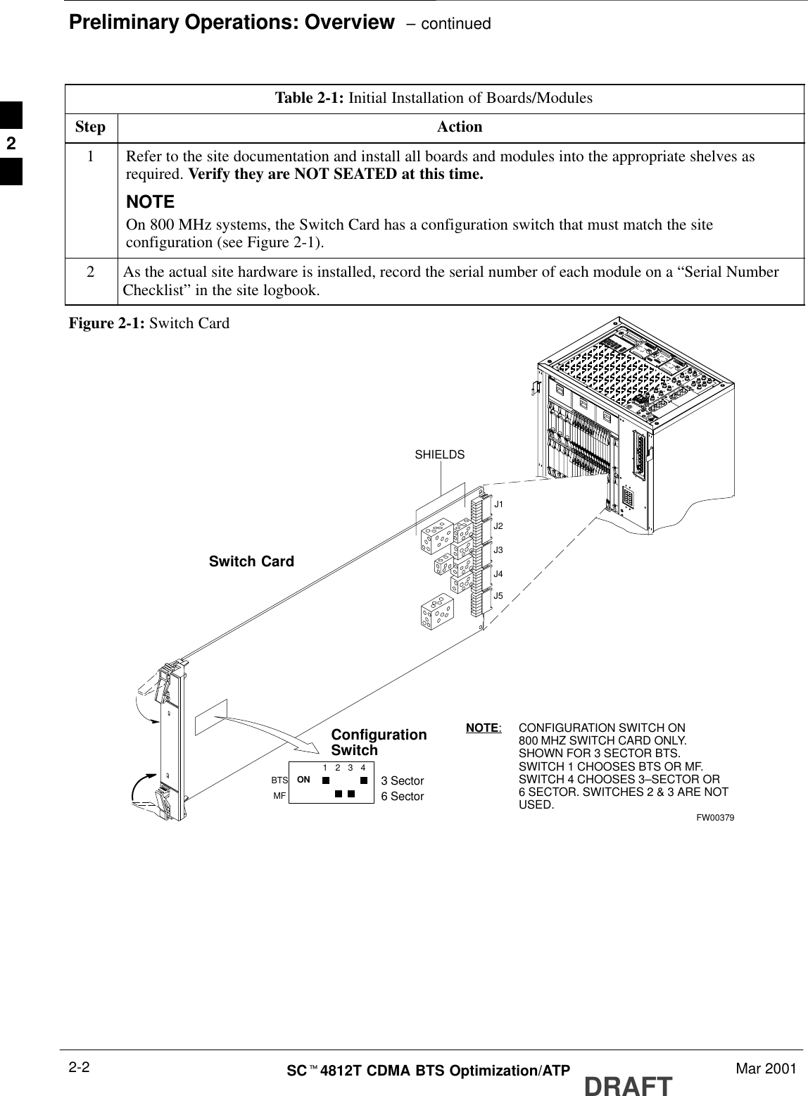
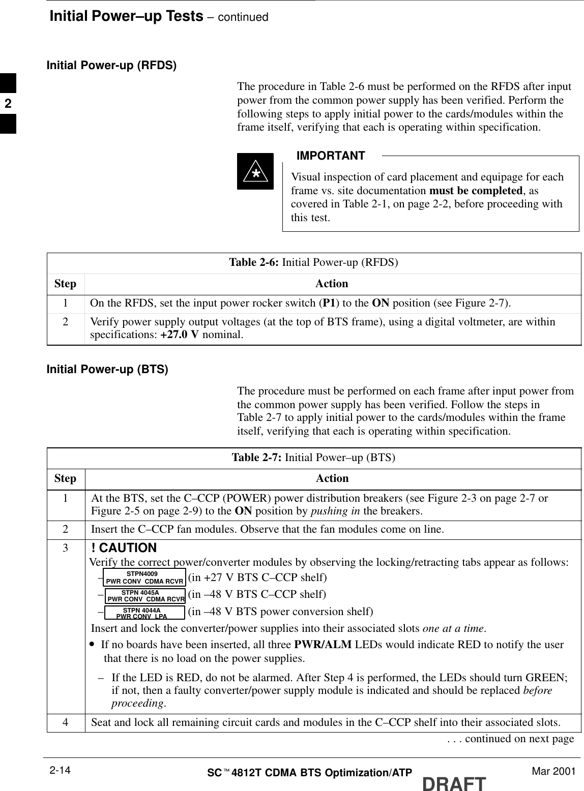
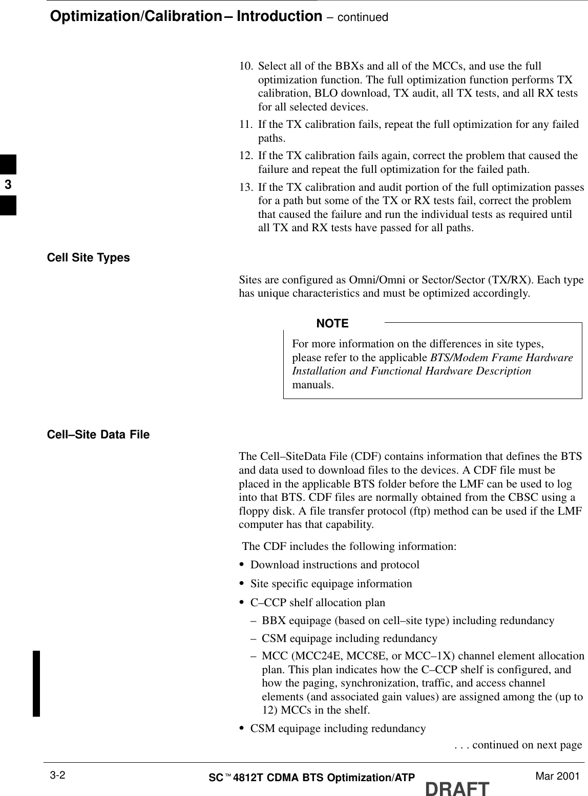
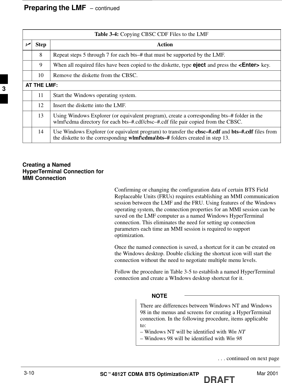
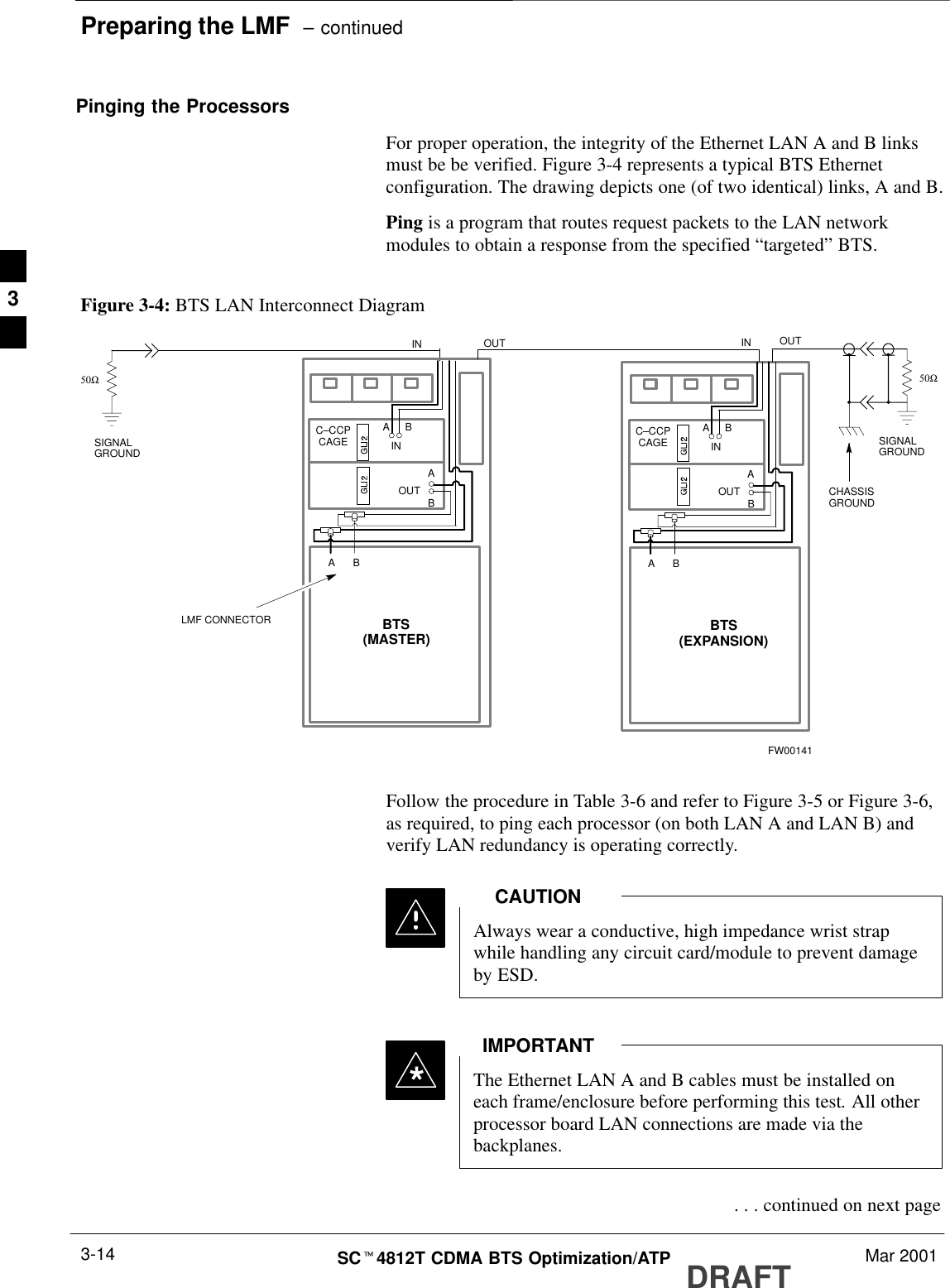
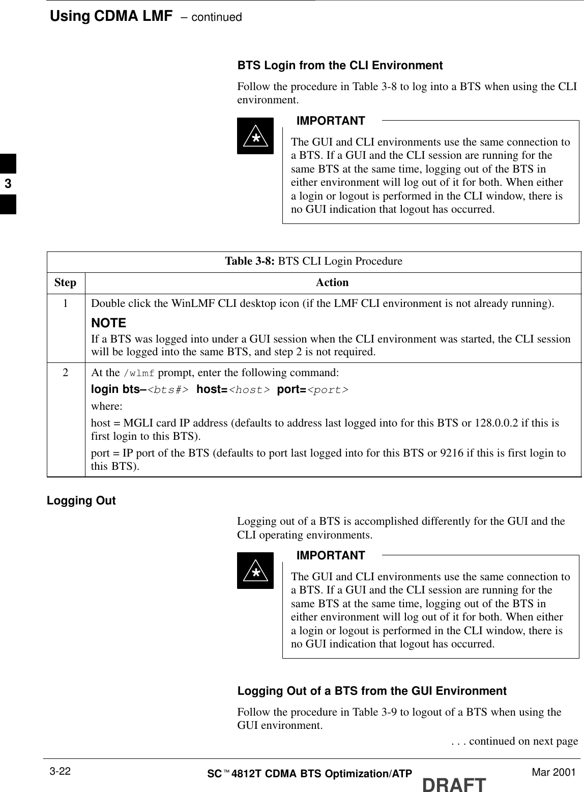
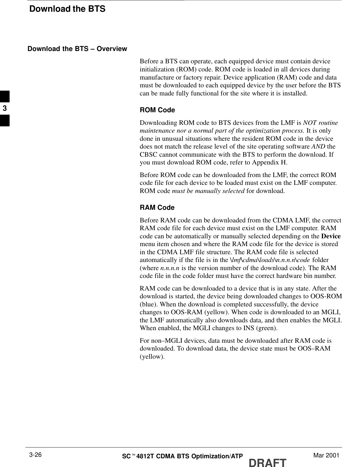
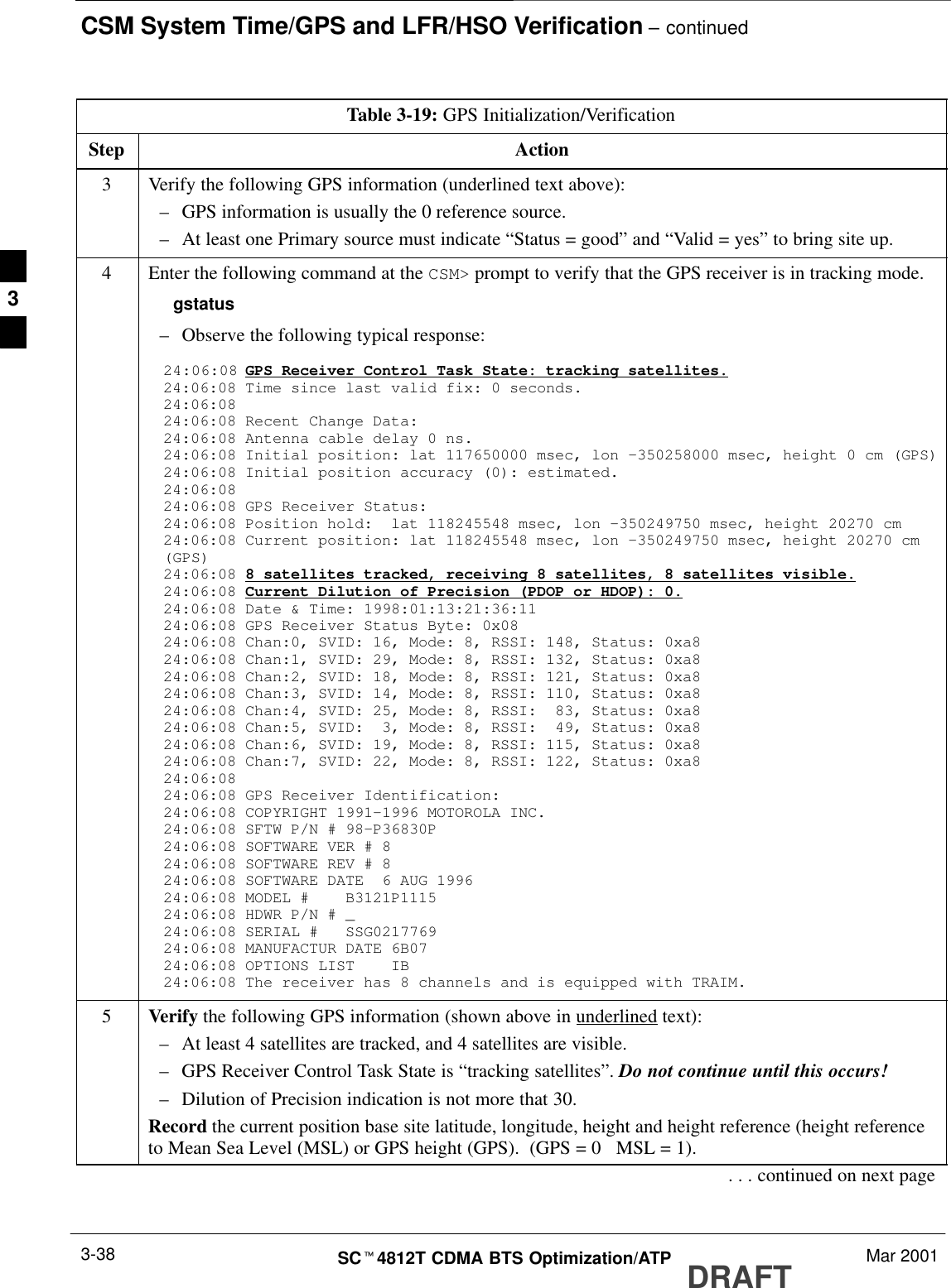
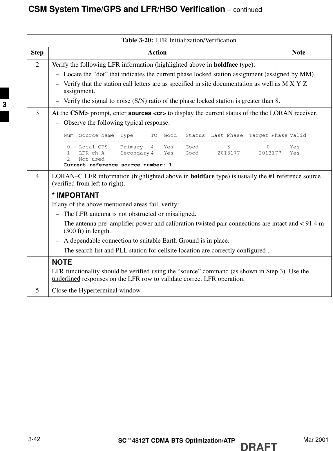
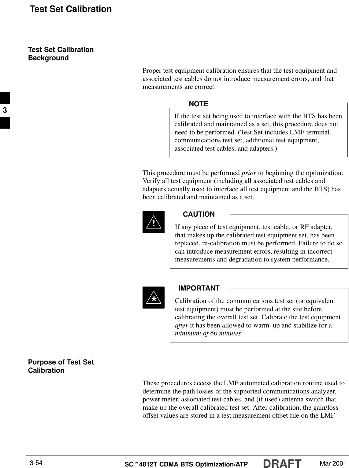
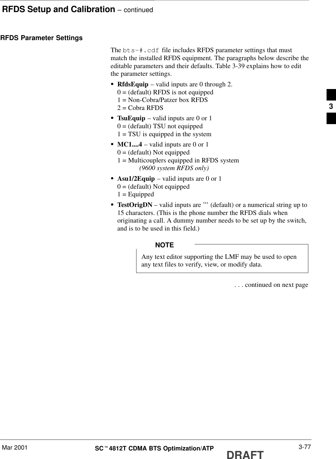
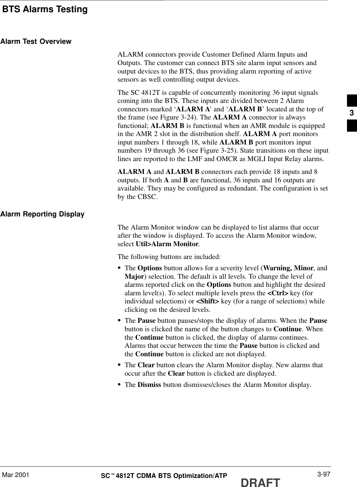
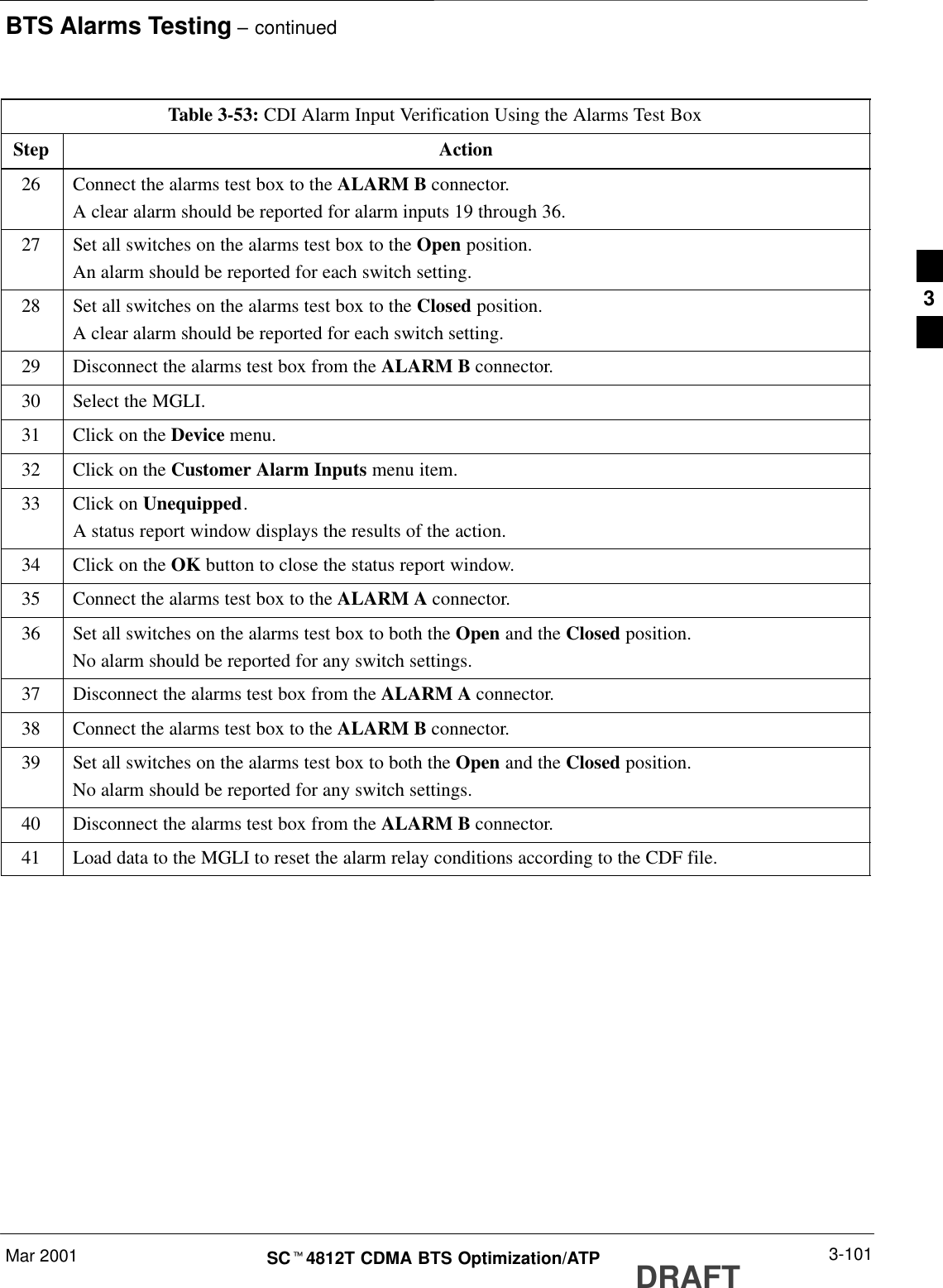
![Bay Level Offset Calibration – continuedDRAFTSCt4812T CDMA BTS Optimization/ATP Mar 20013-66BLO Calibration Data FileDuring the calibration process, the LMF creates a bts–n.cal calibration(BLO) offset data file in the bts–n folder. After calibration has beencompleted, this offset data must be downloaded to the BBXs using theDownload BLO function. An explanation of the file is shown below.Due to the size of the file, Motorola recommends that youprint out a hard copy of a bts.cal file and refer to it for thefollowing descriptions.NOTEThe CAL file is subdivided into sections organized on a per slot basis (aslot Block).Slot 1 contains the calibration data for the 12 BBX slots. Slot 20contains the calibration data for the redundant BBX. Each BBX slotheader block contains:SA creation Date and Time – broken down into separate parameters ofcreateMonth, createDay, createYear, createHour, and createMin.SThe number of calibration entries – fixed at 720 entries correspondingto 360 calibration points of the CAL file including the slot header andactual calibration data.SThe calibration data for a BBX is organized as a large flat array. Thearray is organized by branch, sector, and calibration point.–The first breakdown of the array indicates which branch thecontained calibration points are for. The array covers transmit, mainreceive and diversity receive offsets as follows:Table 3-31: BLO BTS.cal File Array AssignmentsRange AssignmentC[1]–C[240] TransmitC[241]–C[480] Main ReceiveC[481]–C[720] Diversity ReceiveSlot 385 is the BLO for the RFDS.NOTE . . . continued on next page3](https://usermanual.wiki/Nokia-Solutions-and-Networks/T5BL1.IHET5BL1-User-Manual-Part-2-of-3/User-Guide-167838-Page-88.png)
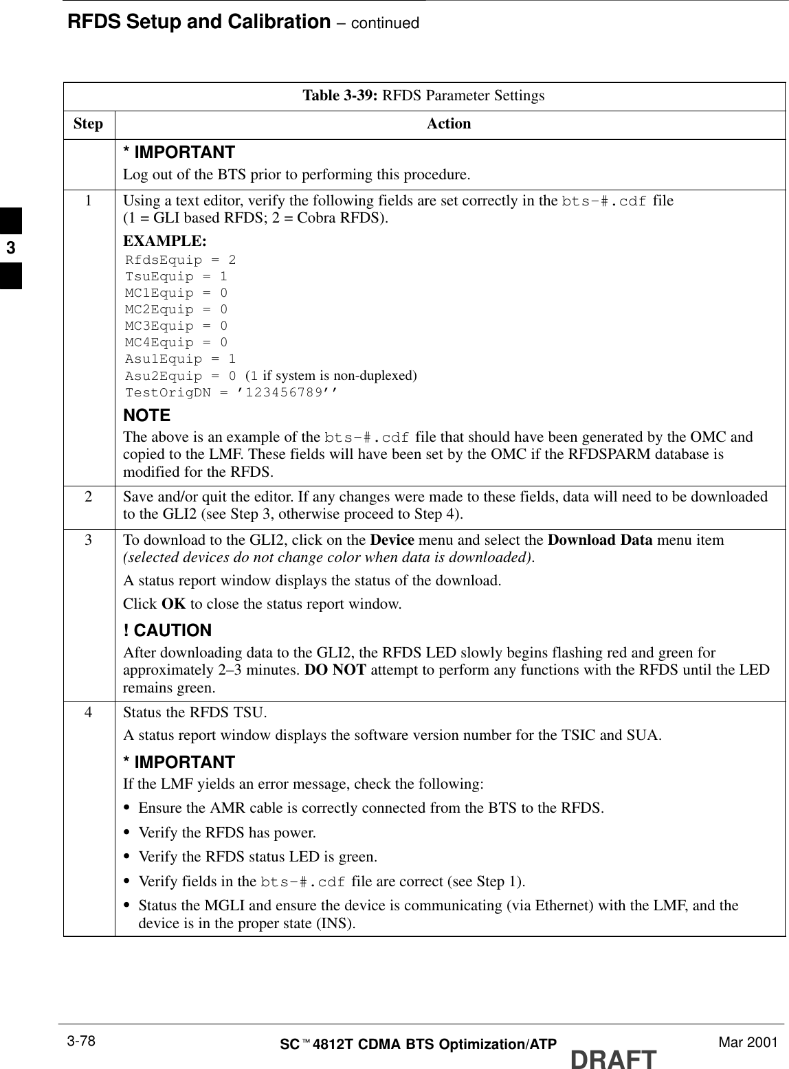
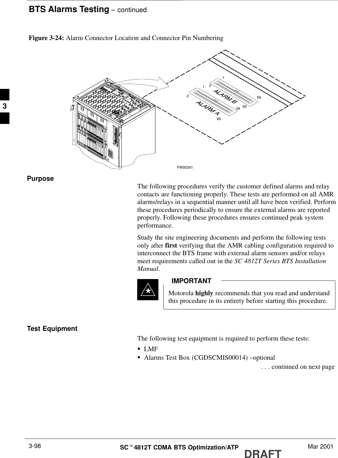
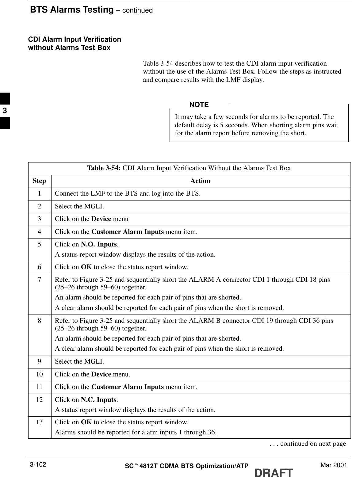
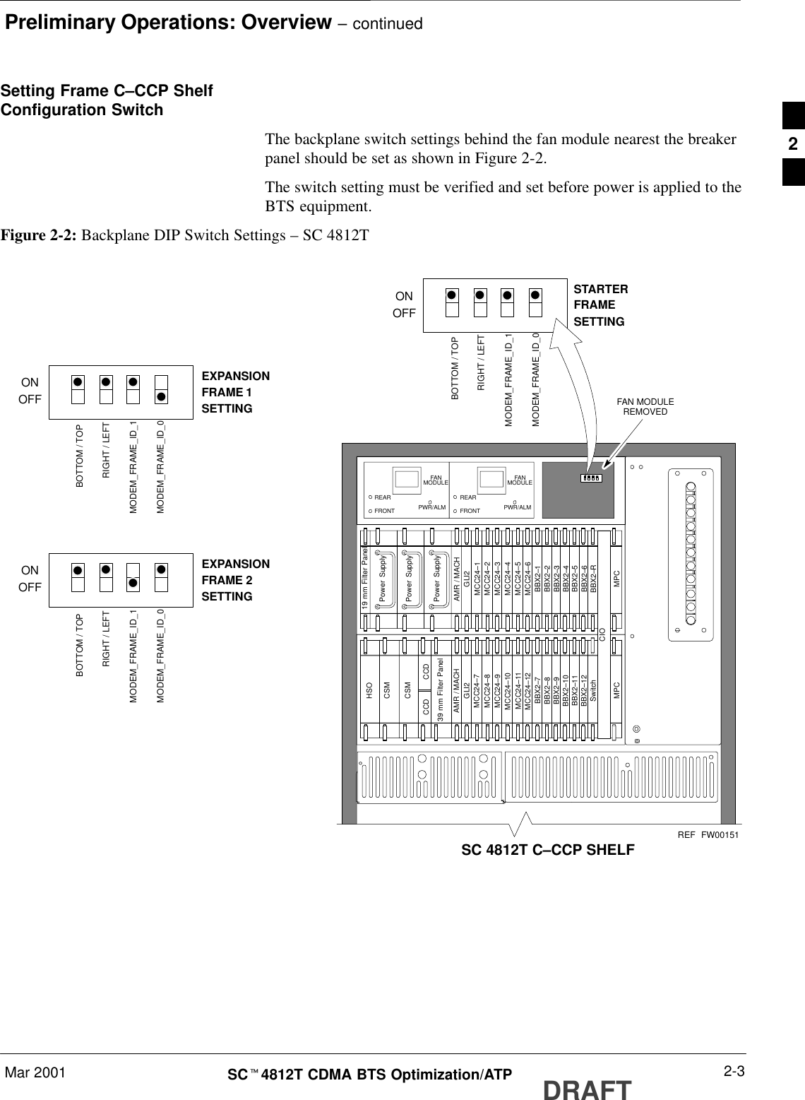
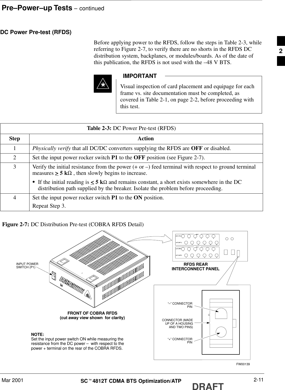
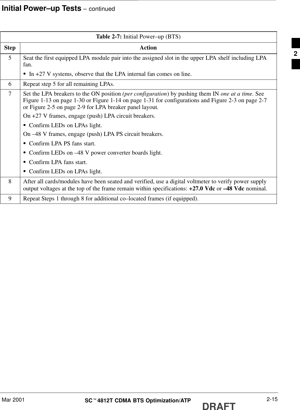
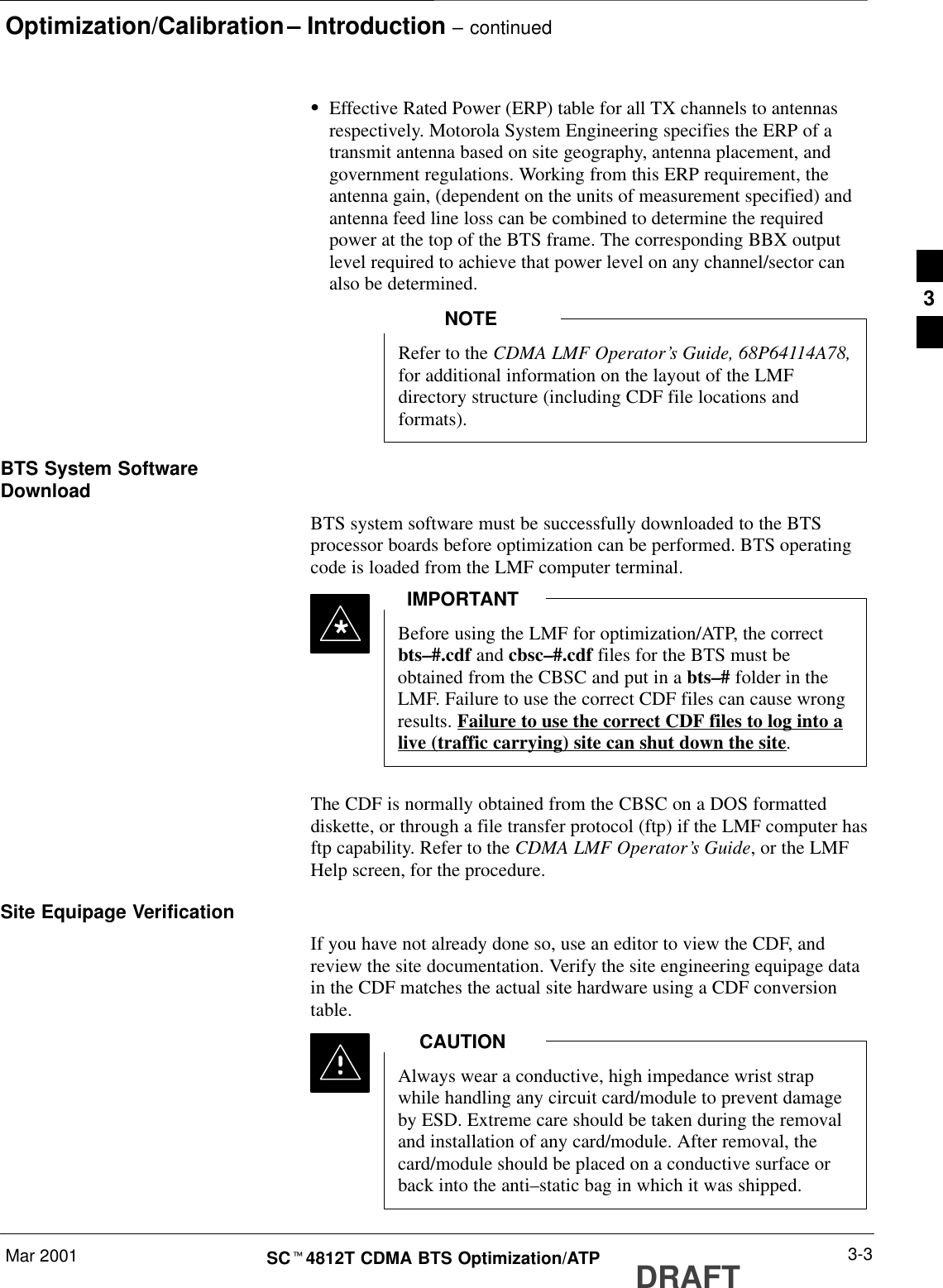
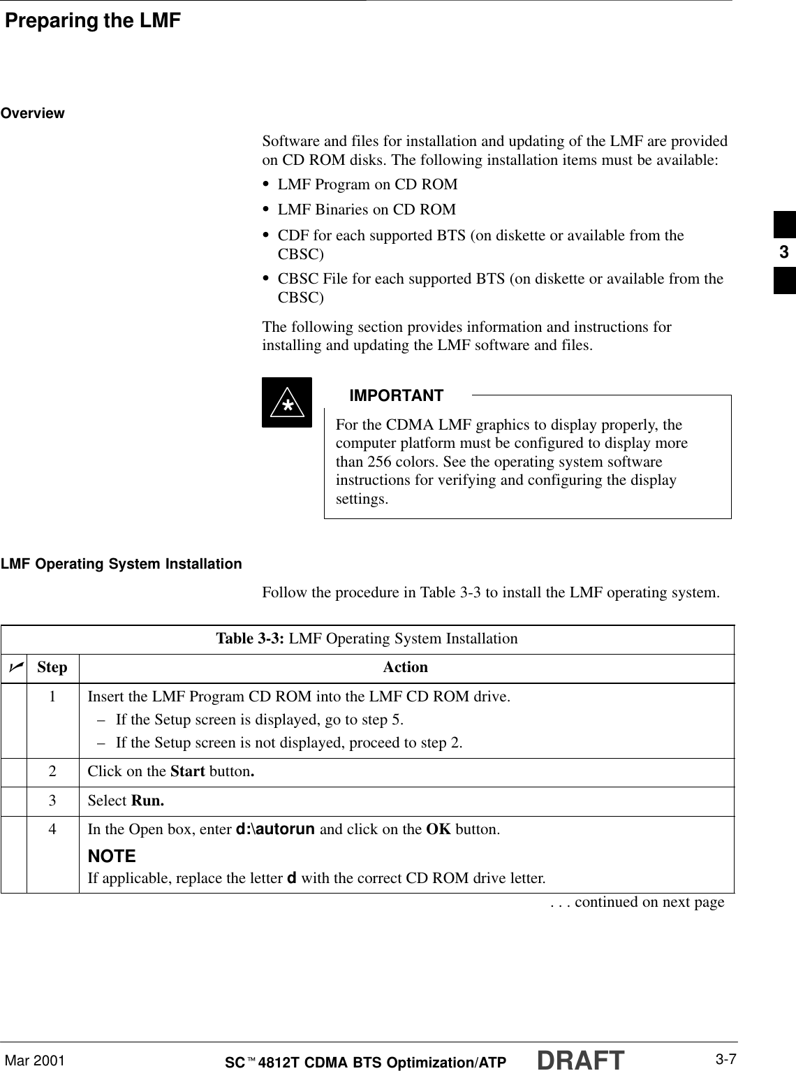
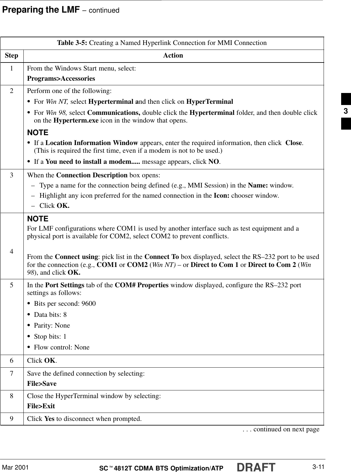
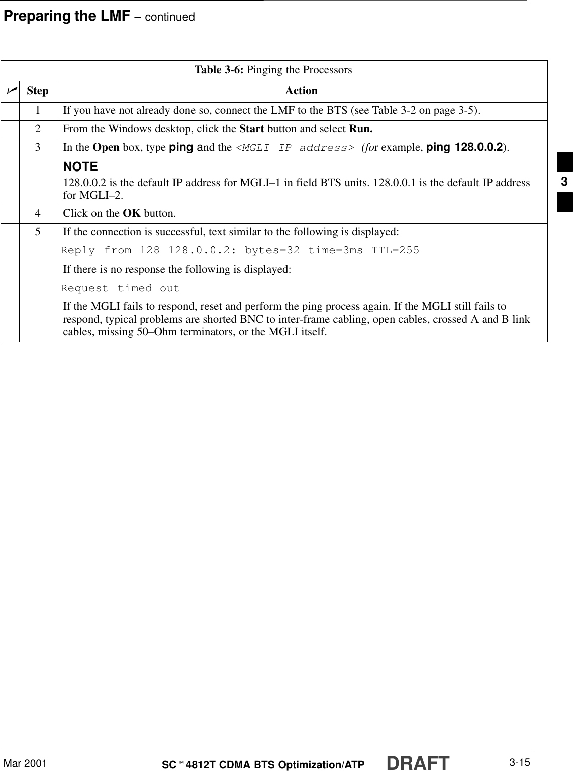
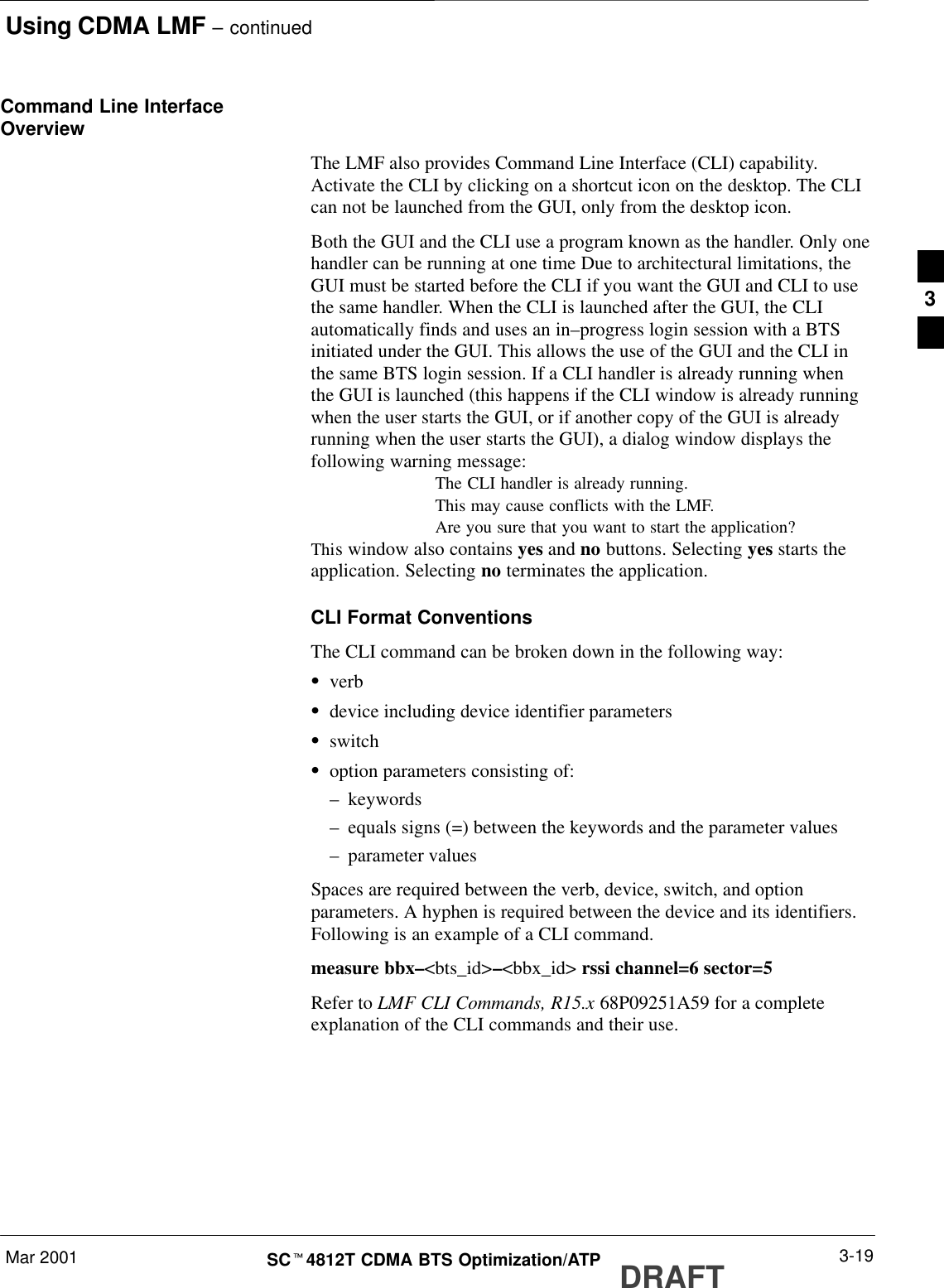
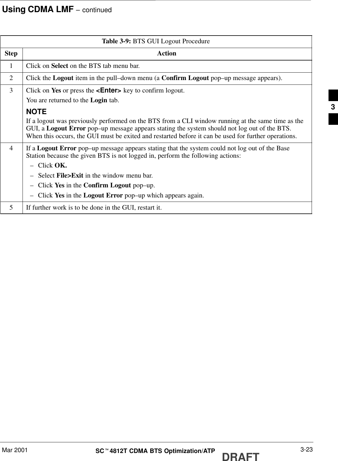
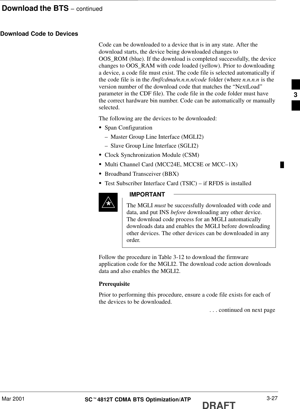
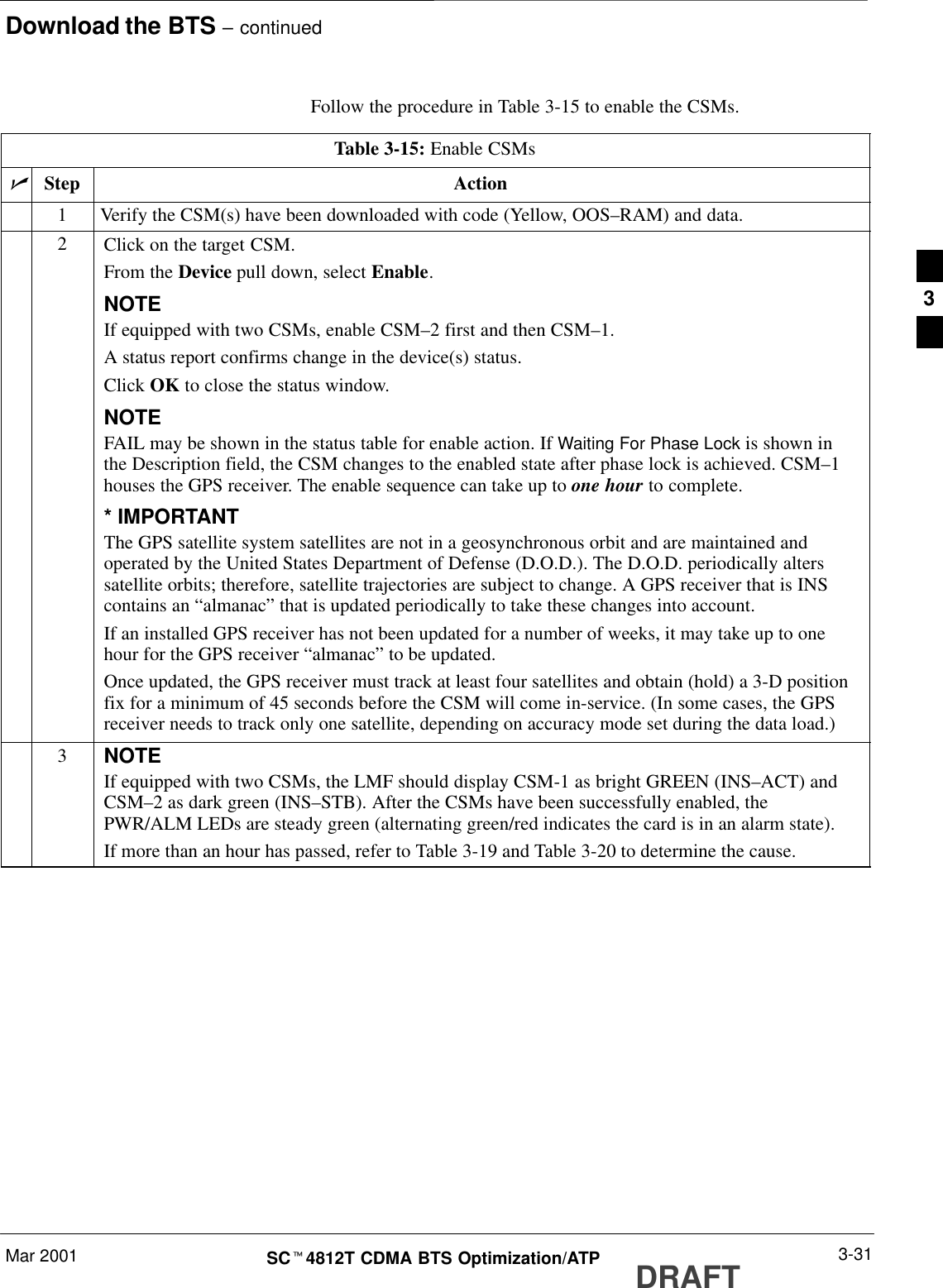
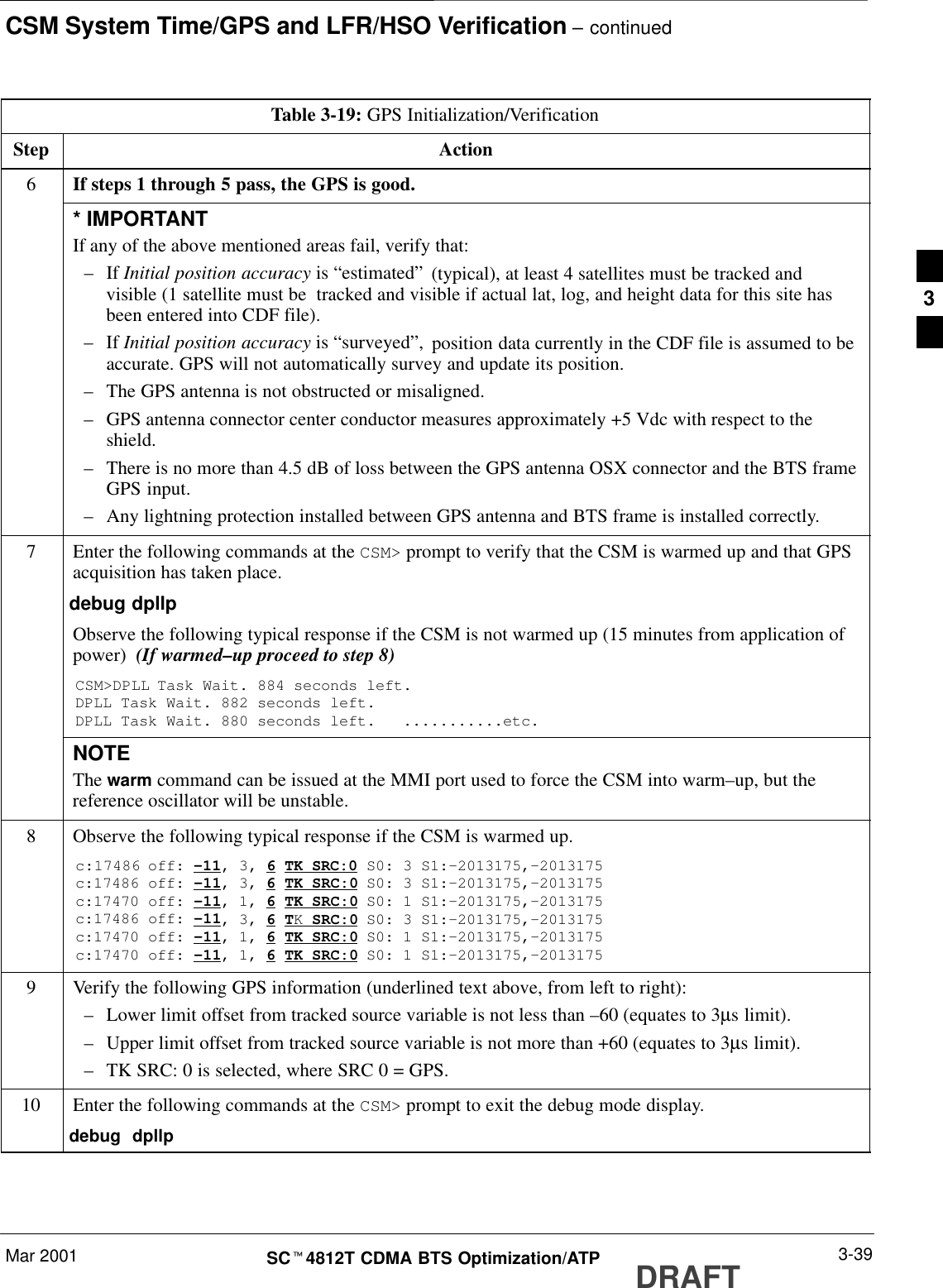
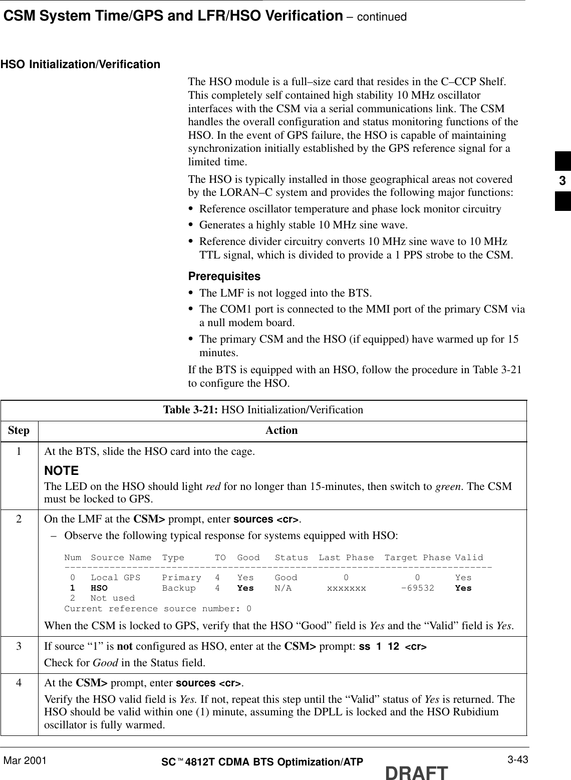
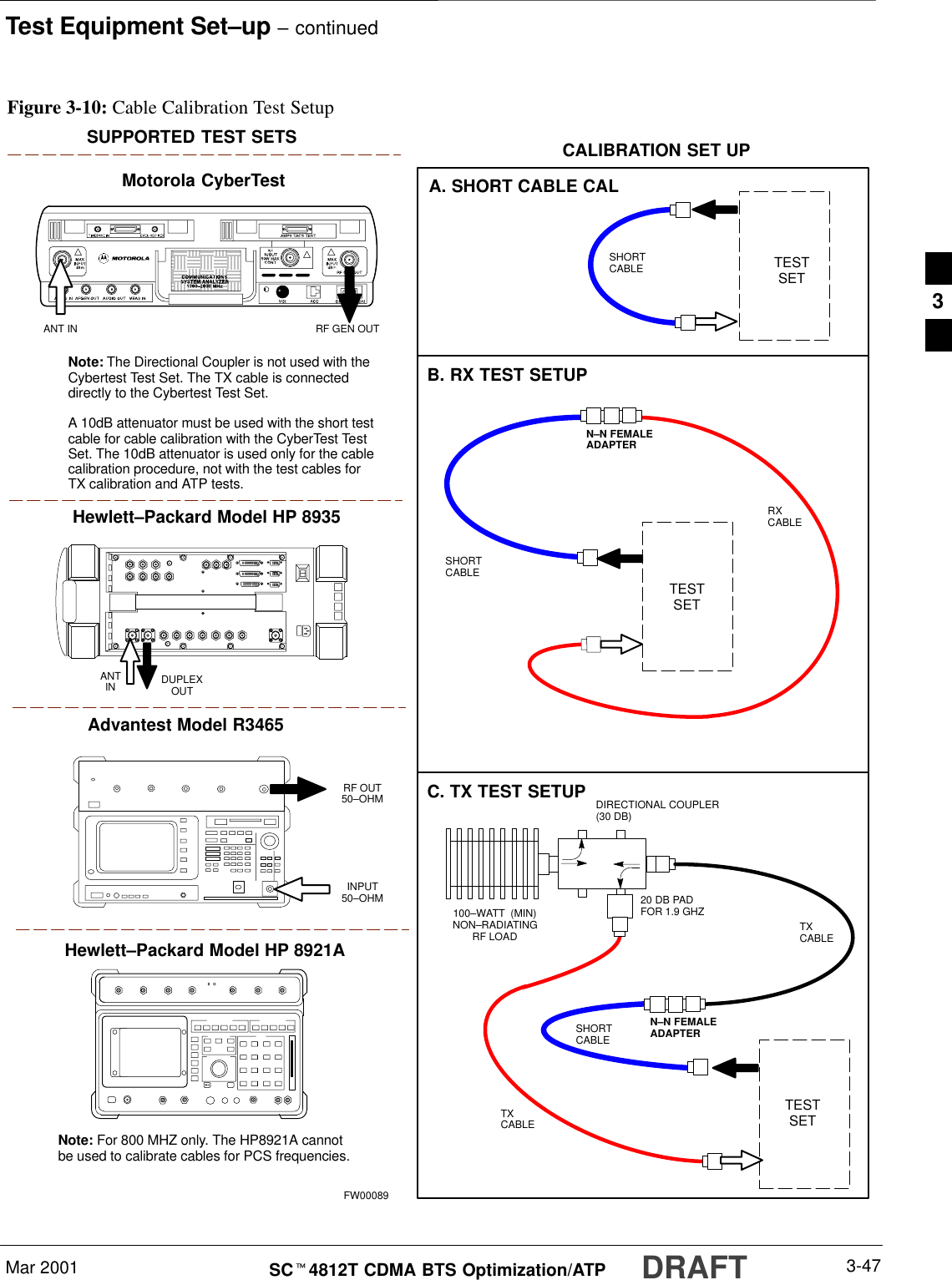
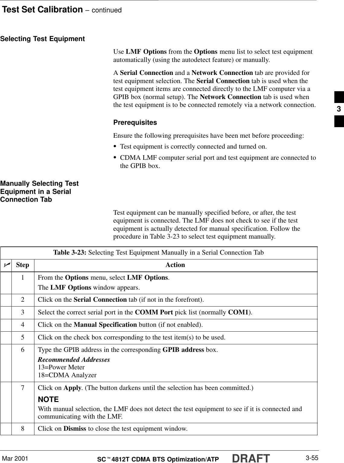
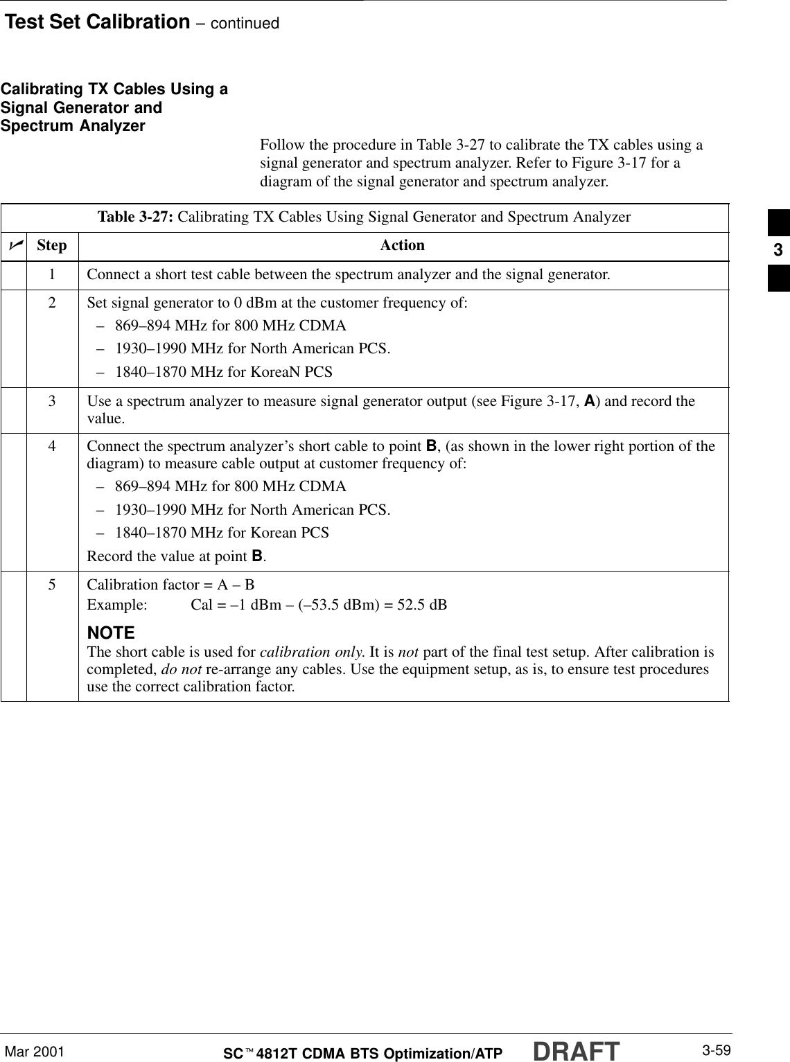
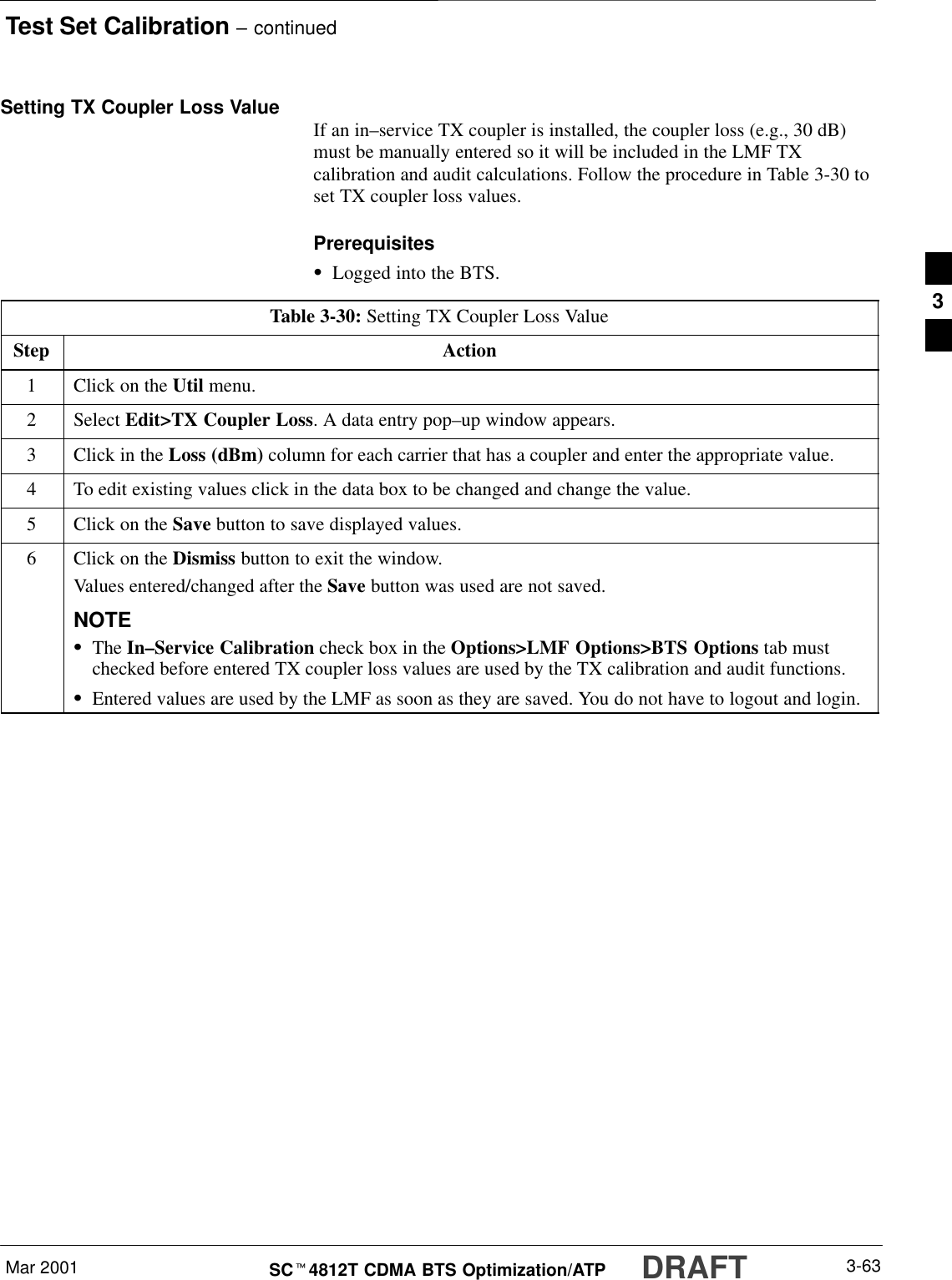
![Bay Level Offset Calibration – continuedMar 2001 3-67SCt4812T CDMA BTS Optimization/ATP DRAFT–The second breakdown of the array is per sector. Configurationssupported are Omni, 3–sector or 6–sector.Table 3-32: BTS.cal File Array (Per Sector)BBX Sectorization TX RX RX DiversitySlot[1] (Primary BBXs 1 through 12)1 (Omni) 3–Sector, C[1]–C[20] C[241]–C[260] C[481]–C[500]23–Sector,1st C[21]–C[40] C[261]–C[280] C[501]–C[520]36 Sector, Carrier C[41]–C[60] C[281]–C[300] C[521]–C[540]41stCarrier 3–Sector, C[61]–C[80] C[301]–C[320] C[541]–C[560]5Carrier 3–Sector,3rd C[81]–C[100] C[321]–C[340] C[561]–C[580]6Carrier C[101]–C[120] C[341]–C[360] C[581]–C[600]73–Sector, C[121]–C[140] C[361]–C[380] C[601]–C[620]83–Sector,2nd C[141]–C[160] C[381]–C[400] C[621]–C[640]96 Sector, Carrier C[161]–C[180] C[401]–C[420] C[641]–C[660]10 2ndCarrier 3–Sector, C[181]–C[200] C[421]–C[440] C[661]–C[680]11 Carrier 3–Sector,4th C[201]–C[220] C[441]–C[460] C[681]–C[700]12 Carrier C[221]–C[240] C[461]–C[480] C[701]–C[720]Slot[20]] (Redundant BBX–13)1 (Omni) 3–Sector, C[1]–C[20] C[241]–C[260] C[481]–C[500]23–Sector,1st C[21]–C[40] C[261]–C[280] C[501]–C[520]36 Sector, Carrier C[41]–C[60] C[281]–C[300] C[521]–C[540]41stCarrier 3–Sector, C[61]–C[80] C[301]–C[320] C[541]–C[560]5Carrier 3–Sector,3rd C[81]–C[100] C[321]–C[340] C[561]–C[580]6Carrier C[101]–C[120] C[341]–C[360] C[581]–C[600]73–Sector, C[121]–C[140] C[361]–C[380] C[601]–C[620]83–Sector,2nd C[141]–C[160] C[381]–C[400] C[621]–C[640]96 Sector, Carrier C[161]–C[180] C[401]–C[420] C[641]–C[660]10 2ndCarrier 3–Sector, C[181]–C[200] C[421]–C[440] C[661]–C[680]11 Carrier 3–Sector,4th C[201]–C[220] C[441]–C[460] C[681]–C[700]12 Carrier C[221]–C[240] C[461]–C[480] C[701]–C[720]STen calibration points per sector are supported for each branch. Twoentries are required for each calibration point.SThe first value (all odd entries) refer to the CDMA channel(frequency) where the BLO is measured. The second value (all evenentries) is the power set level. The valid range for PwrLvlAdj is from2500 to 27500 (2500 corresponds to –125 dBm and 27500corresponds to +125 dBm). . . . continued on next page3](https://usermanual.wiki/Nokia-Solutions-and-Networks/T5BL1.IHET5BL1-User-Manual-Part-2-of-3/User-Guide-167838-Page-89.png)
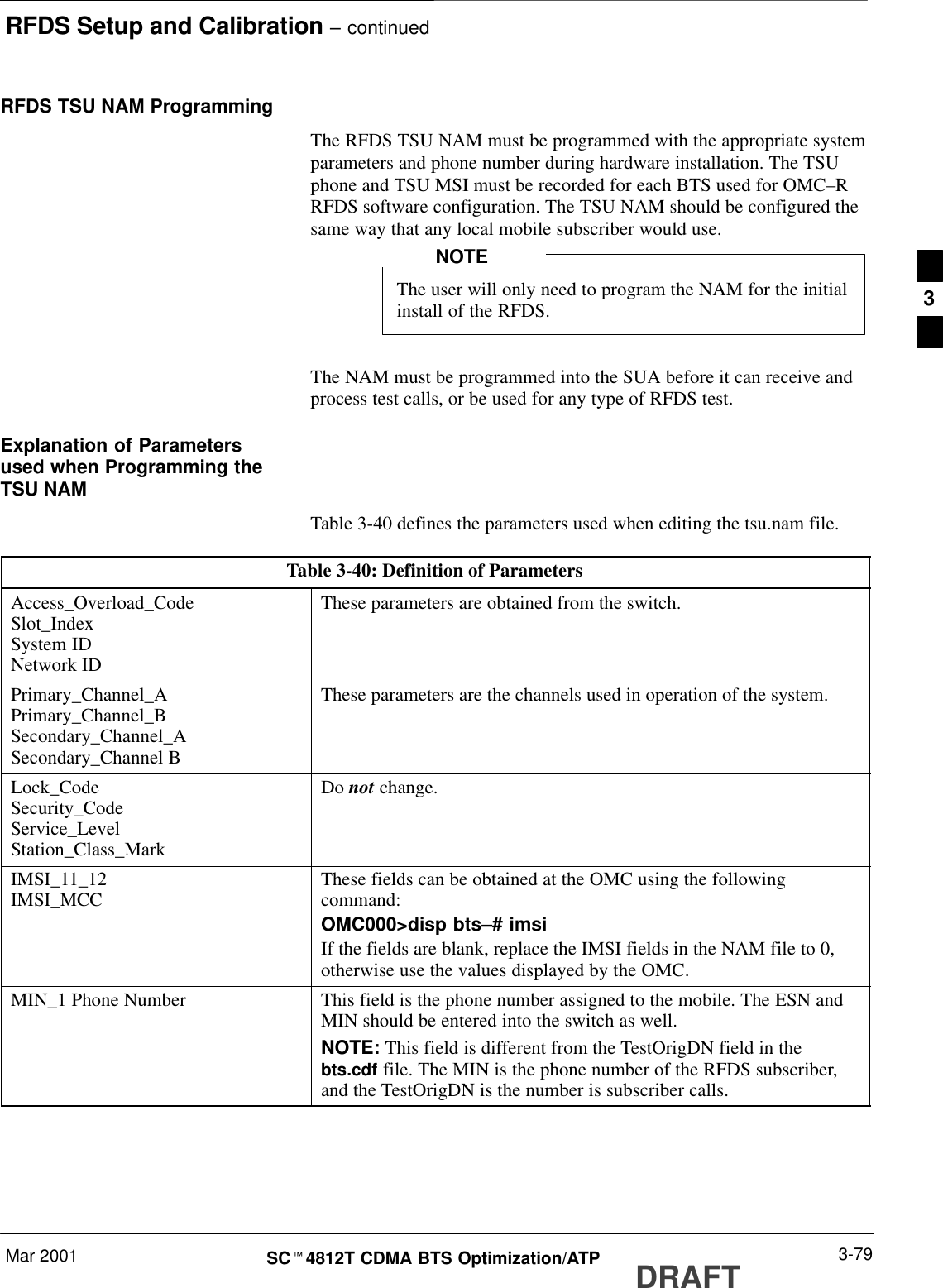
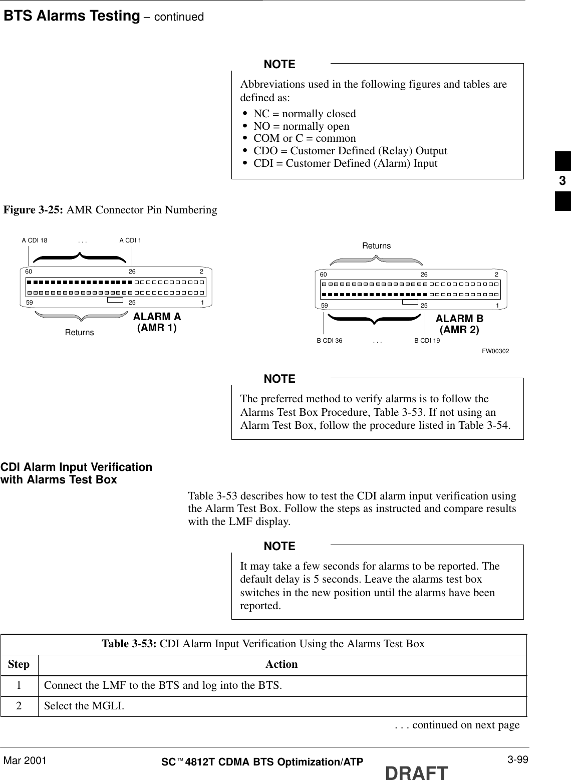
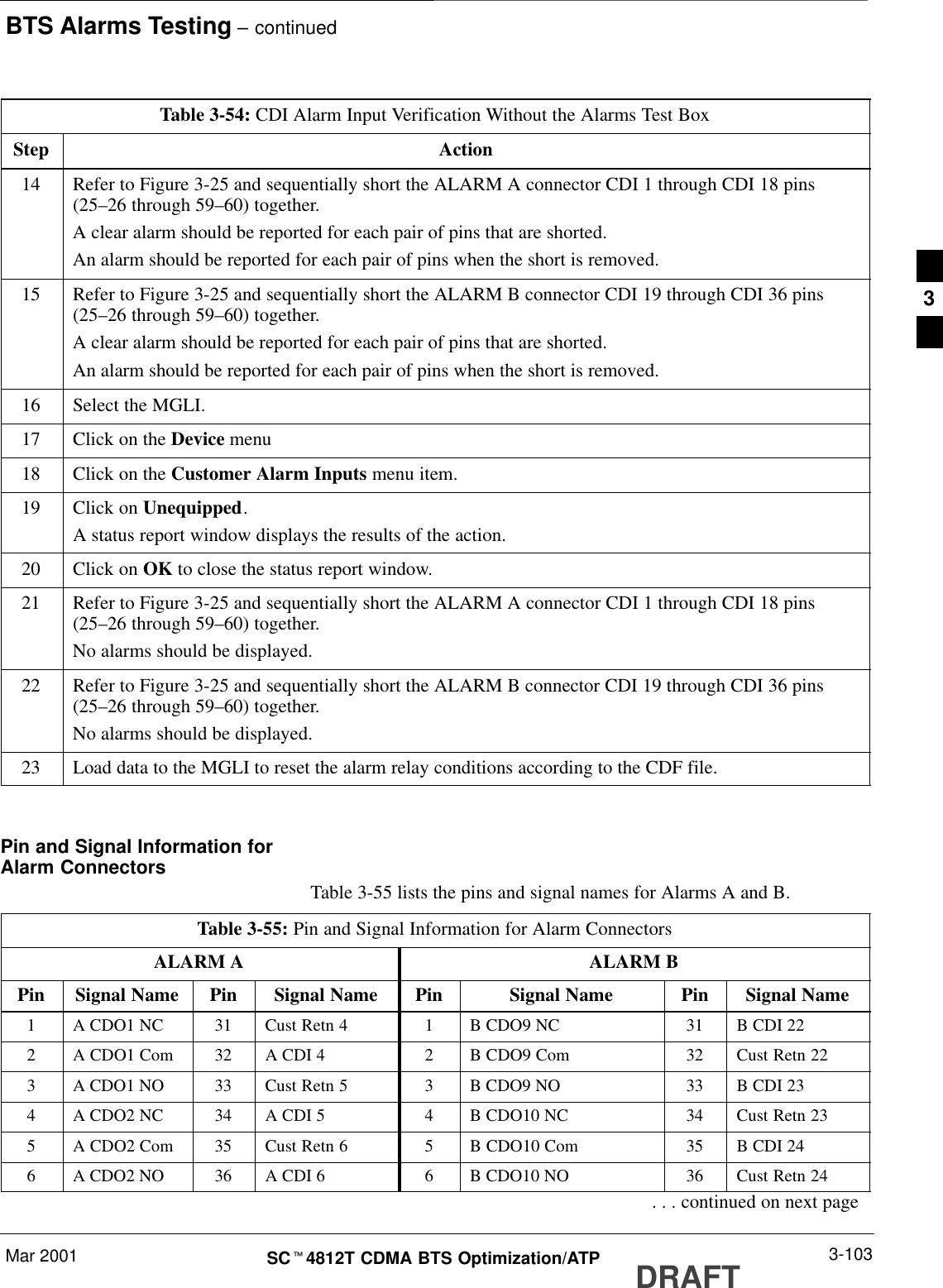
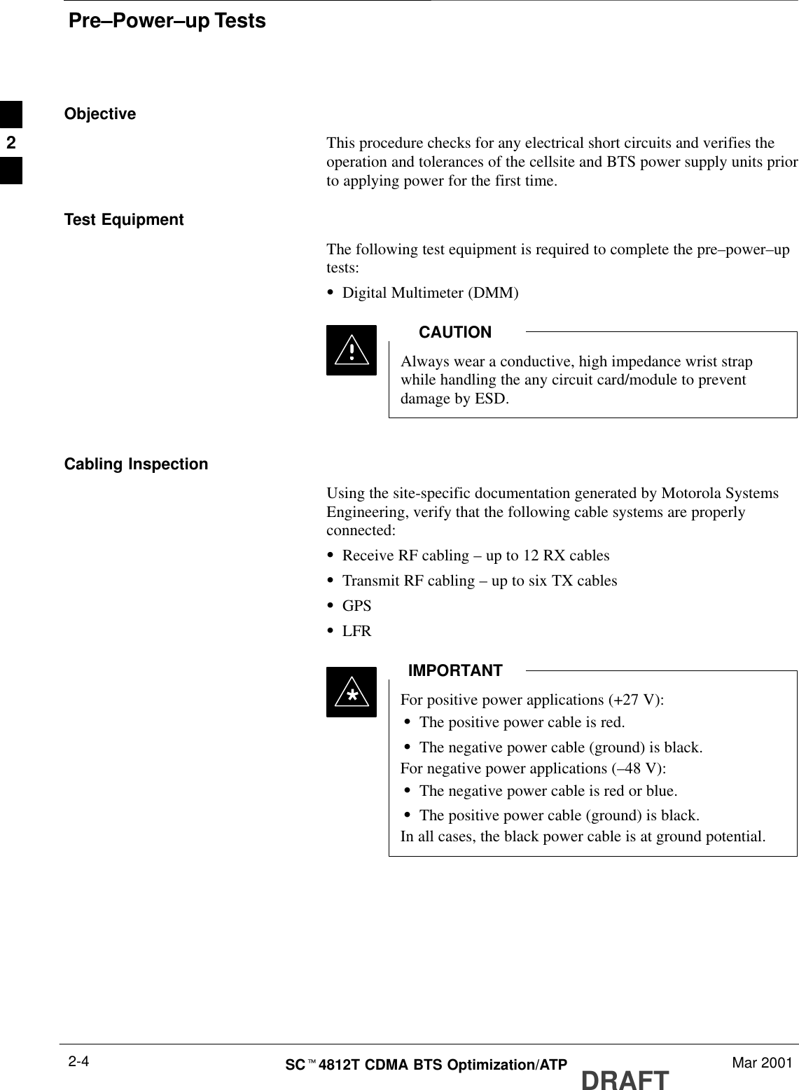
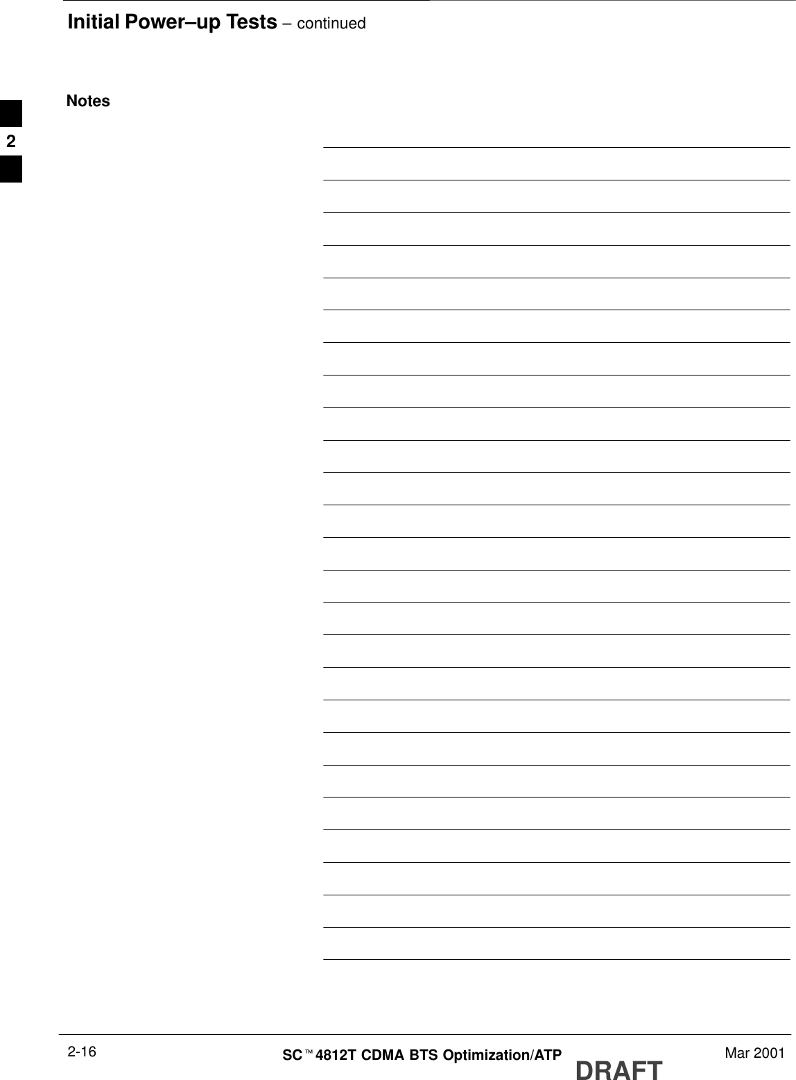
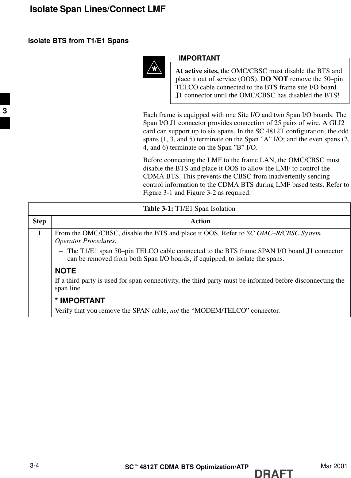
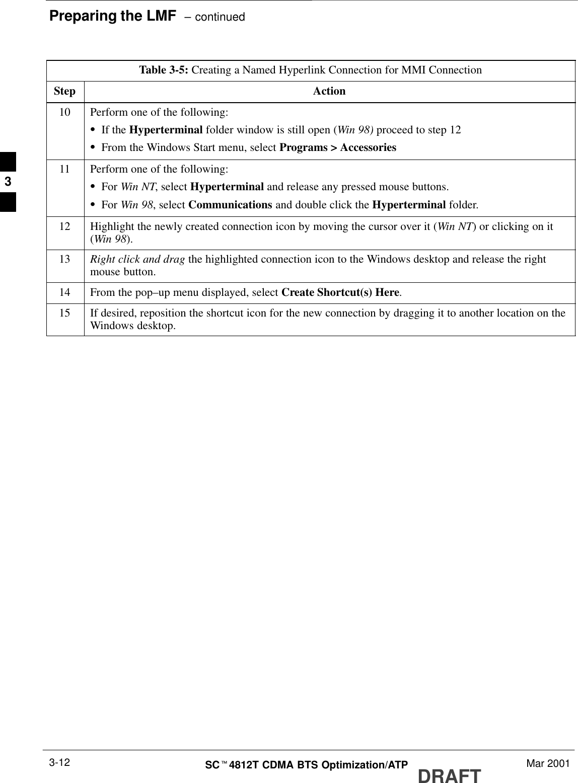
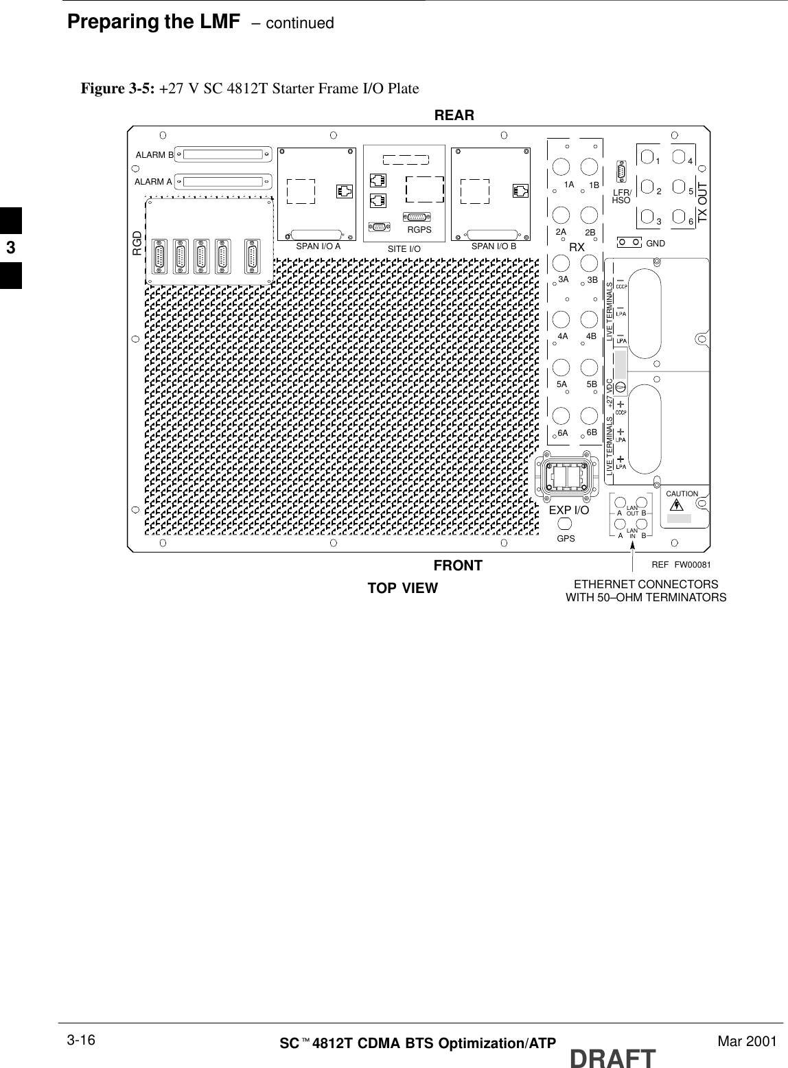
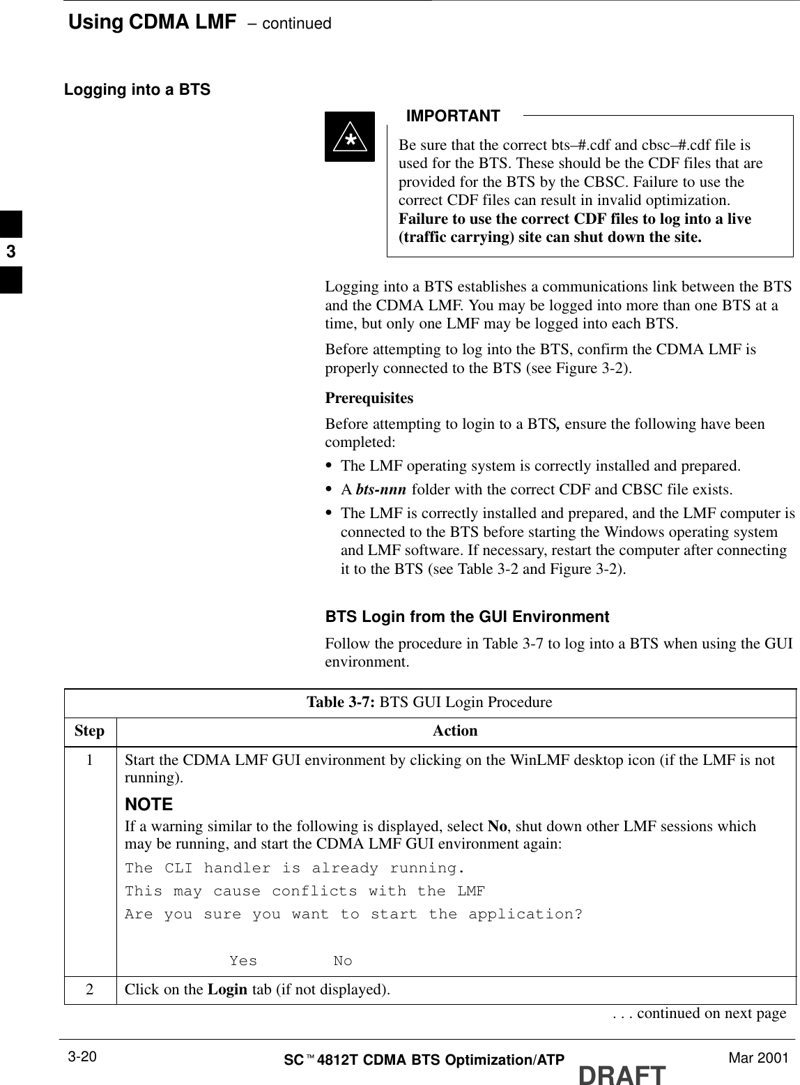
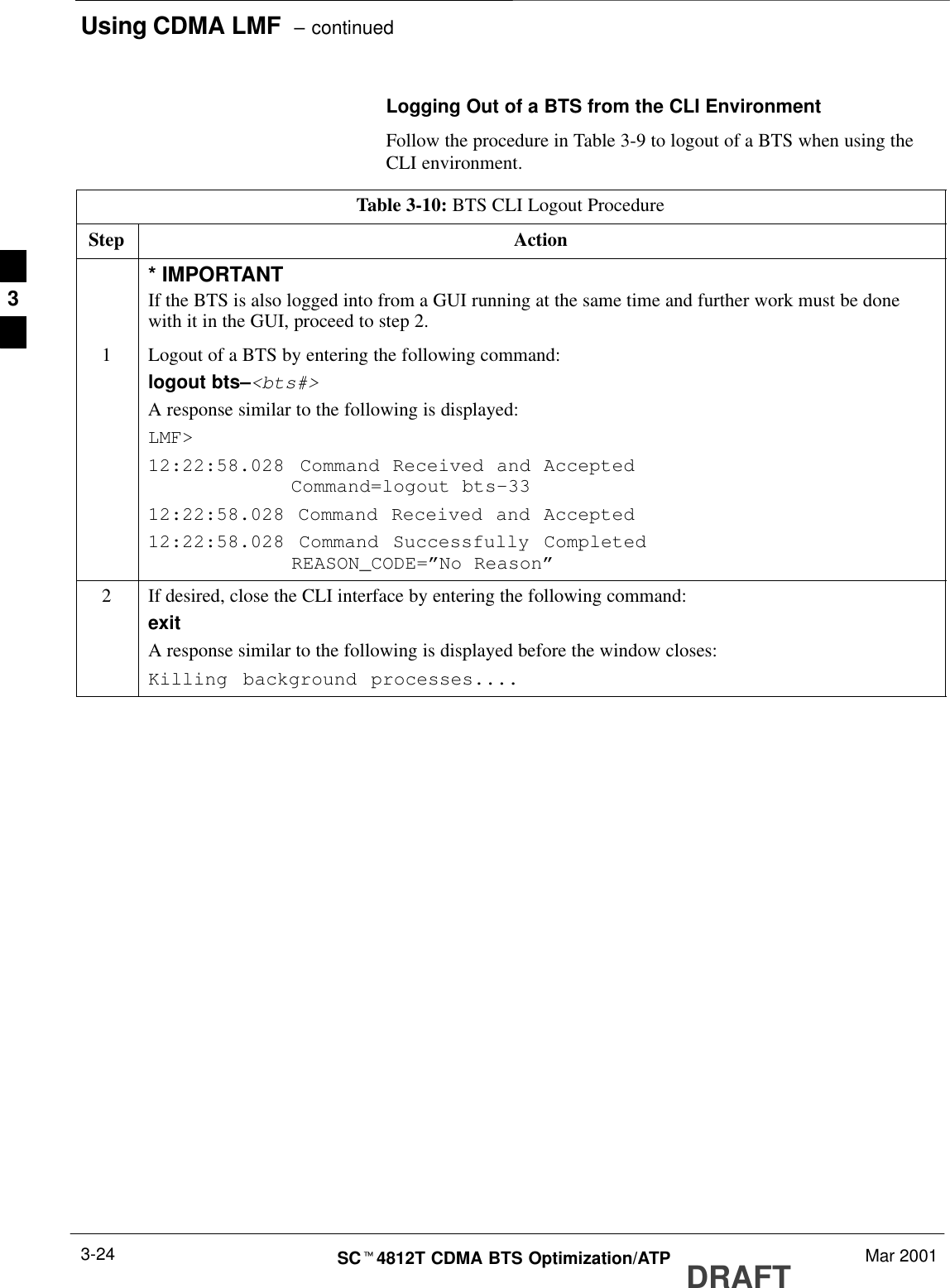
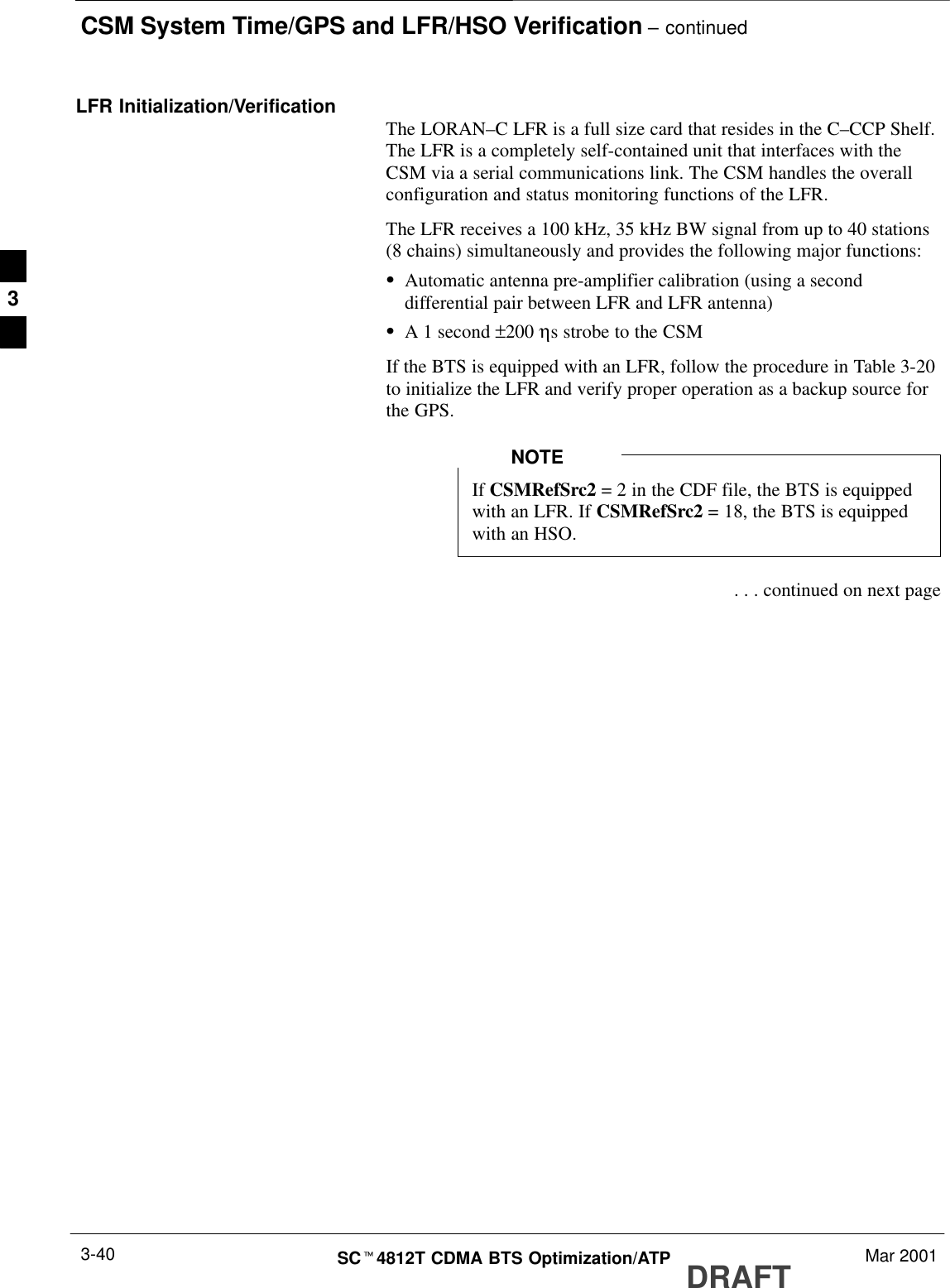
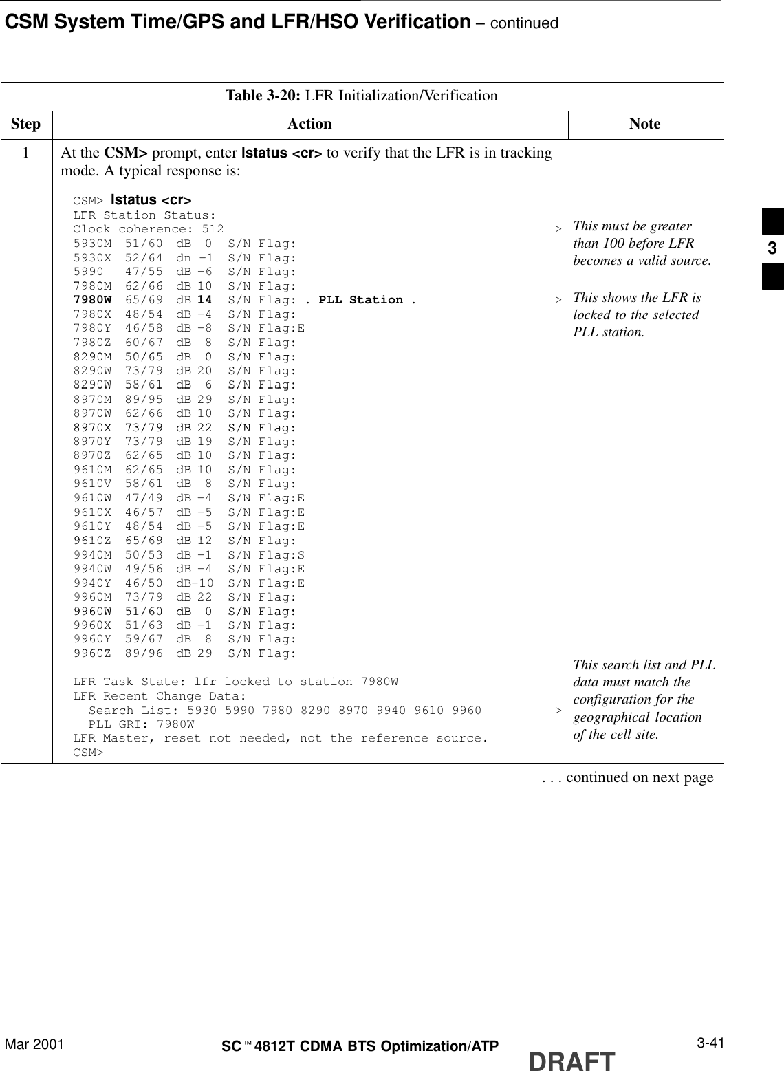
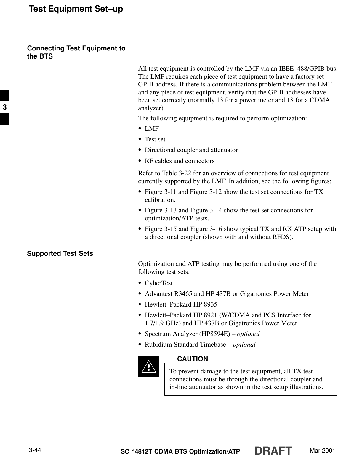
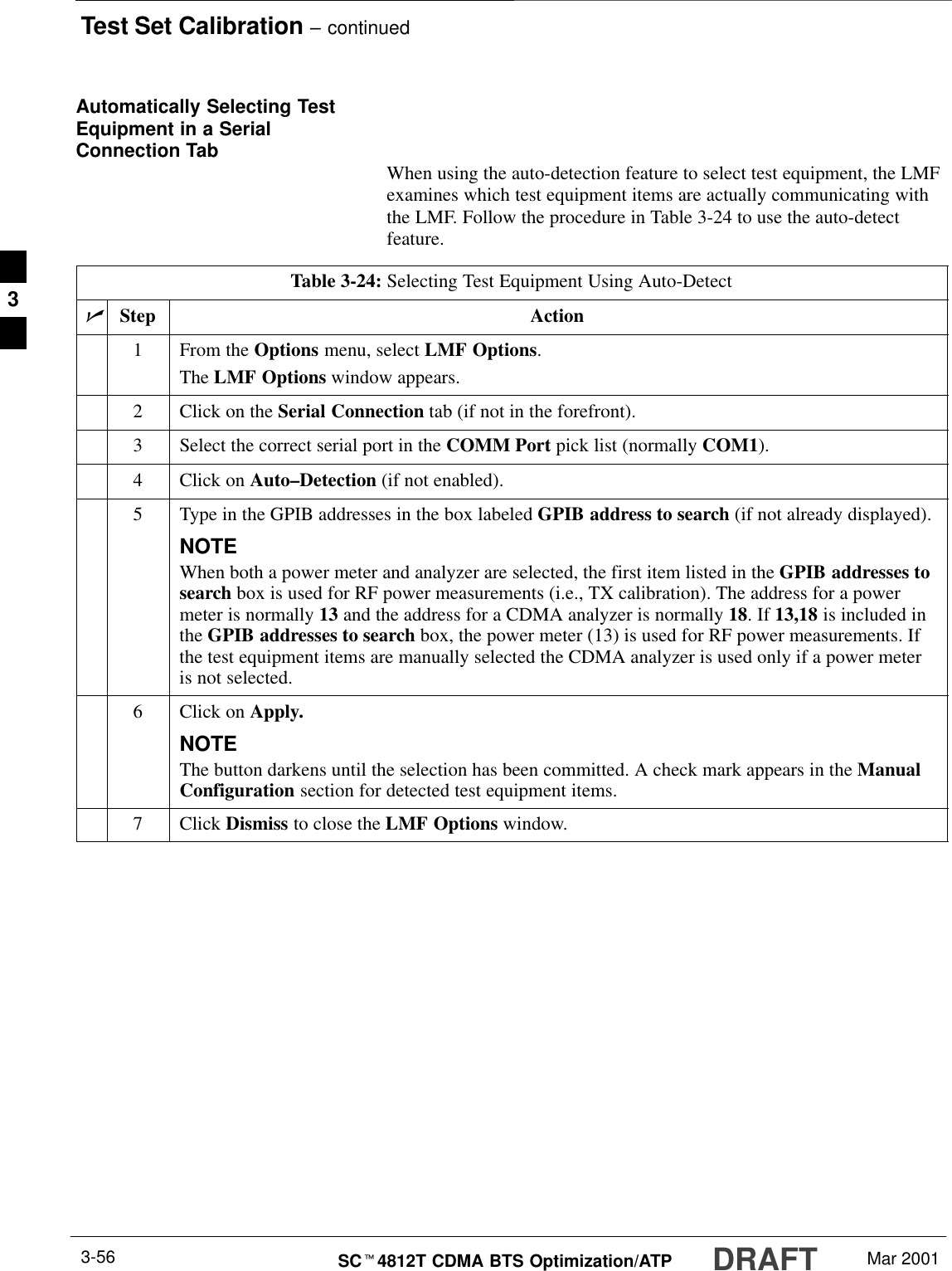
![Bay Level Offset Calibration – continuedDRAFTSCt4812T CDMA BTS Optimization/ATP Mar 20013-68SThe 20 calibration entries for each sector/branch combination must bestored in order of increasing frequency. If less than 10 points(frequencies) are calibrated, the largest frequency that is calibrated isrepeated to fill out the 10 points.Example:C[1]=384, odd cal entry = 1 ‘‘calibration point”C[2]=19102, even cal entryC[3]=777,C[4]=19086,..C[19]=777,C[20]=19086, (since only two cal points were calibrated this would be repeated for the next 8 points)SWhen the BBX is loaded with image = data, the cal file data for theBBX is downloaded to the device in the order it is stored in the calfile. TxCal data is sent first, C[1] – C[240]. Sector 1’s ten calibrationpoints are sent (C[1] – C[20]) followed by sector 2’s ten calibrationpoints (C[21] – C[40]), etc. The RxCal data is sent next (C[241] –C[480]), followed by the RxDCal data (C[481] – C[720]).STemperature compensation data is also stored in the cal file for eachset.Test Equipment Setup:RF Path CalibrationFollow the procedure in Table 3-33 to set up test equipment.Table 3-33: Test Equipment Setup (RF Path Calibration)Step ActionNOTEVerify the GPIB controller is properly connected and turned on.! CAUTIONTo prevent damage to the test equipment, all transmit (TX) test connections must be via the 30 dBdirectional coupler for 800 MHz with an additional 20 dB in–line attenuator for 1.7/1.9 GHz.1Connect the LMF computer terminal to the BTS LAN A connector on the BTS (if you have notalready done so). Refer to the procedure in Table 3–2 on page 3-6.SIf required, calibrate the test equipment per the procedure in Table 3-25 on page 3-57.SConnect the test equipment as shown in Figure 3-11 and Figure 3-12 starting on page 3-48.3](https://usermanual.wiki/Nokia-Solutions-and-Networks/T5BL1.IHET5BL1-User-Manual-Part-2-of-3/User-Guide-167838-Page-90.png)