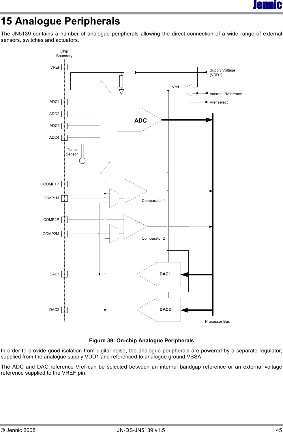
NXP Laboratories UK JN5139M4 IEEE 802.15.4 High Power Wireless Microcontroller User Manual JN DS JN5139 1v5c
NXP Laboratories UK Ltd IEEE 802.15.4 High Power Wireless Microcontroller JN DS JN5139 1v5c
UserManual.wiki
>
NXP Laboratories UK
>
JN5139M4 User Manual
>
manual
Contents
1.
User Manual
2.
Manual
3.
Antenna Info 1
4.
Antenna Info 2
5.
Antenna Info 3
6.
Antenna Info 4
7.
Antenna Info 5
8.
Antenna Info 6
9.
Antenna Info 7
10.
Antenna Info 8
11.
Antenna Info 9
12.
manual
13.
Antenna Info 10
14.
Antenna Info 11
manual
Navigation menu
Upload a User Manual
Namespaces
Wiki Guide
HTML
PDF
Info
Views
User Manual
Discussion / Help
Navigation
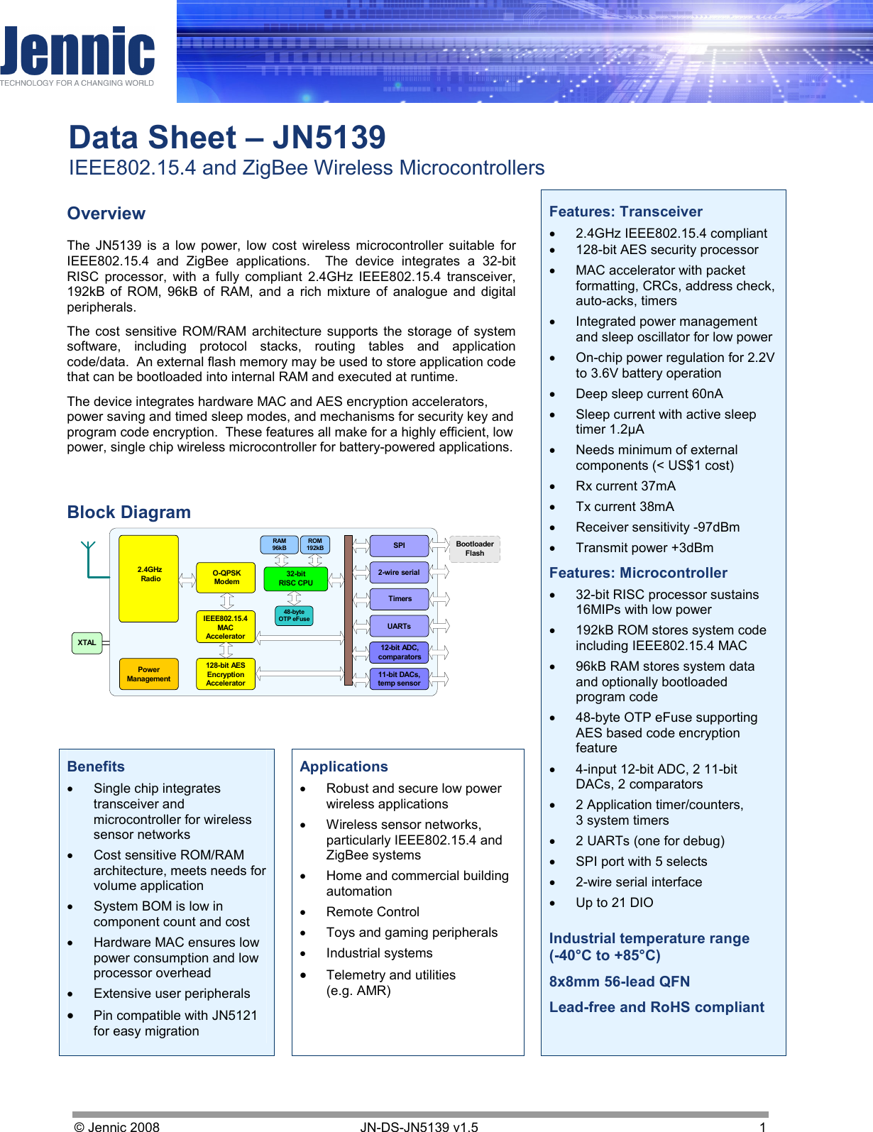
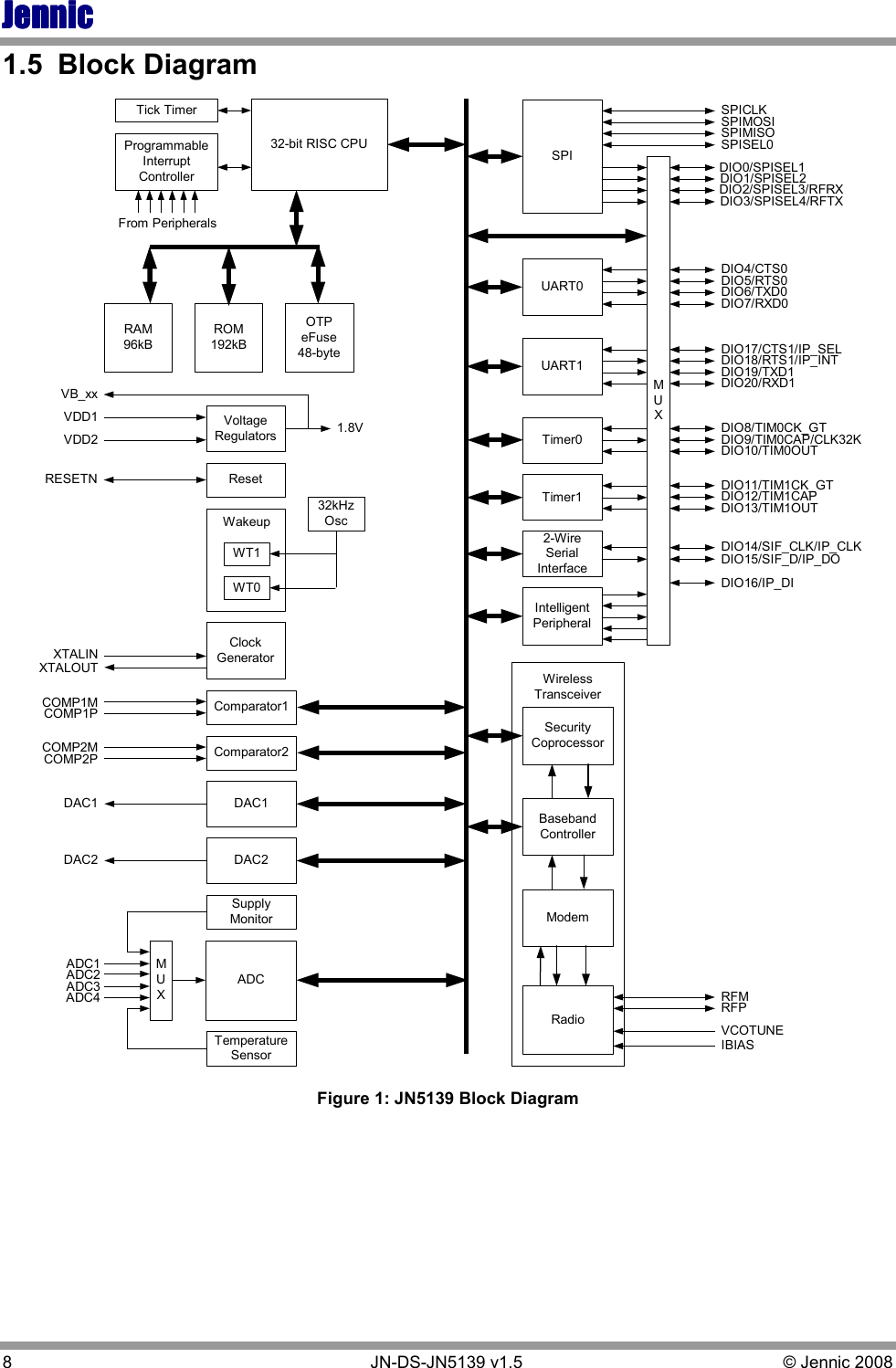
![JennicJennicJennicJennic 6 JN-DS-JN5139 v1.5 © Jennic 2008 1 Introduction The JN5139 is an IEEE802.15.4 wireless microcontroller that provides a fully integrated solution for applications using the IEEE802.15.4 standard in the 2.4 - 2.5GHz ISM frequency band [1], including ZigBee. It includes all of the functionality required to meet the IEEE802.15.4 specification and has additional processor capability to run a wide range of applications including but not limited to Remote Control, Home and Building Automation, Toys and Gaming. The device includes a Wireless Transceiver, RISC CPU, on-chip memory and an extensive range of peripherals. 1.1 Wireless Microcontroller Applications that transfer data wirelessly tend to be more complex than wired ones. Wireless protocols make stringent demands on frequencies, data formats, timing of data transfers, security and other issues. Application development must consider the requirements of the wireless network in addition to the product functionality and user interfaces. To minimise this complexity, Jennic provides a series of software libraries and interfaces that control the transceiver and peripherals of the JN5139. These libraries and interfaces remove the need for the developer to understand wireless protocols and greatly simplifies the programming complexities of power modes, interrupts and hardware functionality. In view of the above, the register details of the JN5139 are not provided in the datasheet. 1.2 Wireless Transceiver The Wireless Transceiver is highly integrated and, together with the integrated IEEE802.15.4 MAC library contained in ROM requires little knowledge of RF or wireless design. The Wireless Transceiver comprises a low-IF 2.45GHz radio, an O-QPSK modem, a baseband controller and a security coprocessor. The radio has a 200Ω resistive differential antenna port that includes all the required matching components on-chip, allowing a differential antenna to be connected directly to the port, minimising the system BOM costs. Connection to a single ported antenna can be achieved using a 200/50Ω 2.45GHz balun. In addition, the radio also provides an output to control transmit-receive switching of external devices such as power amplifiers allowing applications that require increased transmit power to be realised very easily. The Security coprocessor provides hardware-based 128-bit AES-CCM, CBC(1), CTR and CCM* processing as specified by the IEEE802.15.4 standard. It does this in-band on packets during transmission and reception, requiring minimal intervention from the CPU. It is also available for off-line use under software control for encrypting and decrypting packets generated by software layers such as Zigbee and user applications. This means that these algorithms can be off-loaded by the CPU, increasing the processor bandwidth available for user applications. The transceiver elements (radio, modem and baseband) work together to provide IEEE802.15.4 Medium Access Control under the control of a protocol stack. (1) AES-CBC processing is only available off-line for use under software control. 1.3 RISC CPU and Memory A 32-bit RISC CPU allows software to be run on-chip, its processing power being shared between the IEEE802.15.4 MAC protocol, other higher layer protocols and the user application. The JN5139 has a unified memory architecture, code memory, data memory, peripheral devices and I/O ports are organized within the same linear address space. The device contains 192kBytes of ROM, 96kBytes of RAM and a 48-byte OTP eFuse memory.](https://usermanual.wiki/NXP-Laboratories-UK/JN5139M4.manual/User-Guide-1094185-Page-6.png)
![JennicJennicJennicJennic 12 JN-DS-JN5139 v1.5 © Jennic 2008 VDD1AnalogueI/O PinVSSAAnaloguePeripheral Figure 3 Analogue I/O Cell 2.2.6 Digital Input/Output Digital I/O pins on the JN5139 can have signals applied up to 2V higher than VDD2 (with the exception of pins DIO9 and DIO10 that are 3V tolerant) and are therefore TTL-compatible with VDD2 > 3V. For other DC properties of these pins see section 17.2.3 I/O Characteristics. When used in their primary function all Digital Input/Output pins are bi-directional and are connected to weak internal pull up resistors (40kΩ nominal) that can be disabled. When used in their secondary function (selected when the appropriate peripheral block is enabled) then their direction is fixed by the function. The pull up resistor is enabled or disabled independently of the function and direction. A schematic view of the digital I/O cell is in Figure 4: DIO Pin Equivalent Schematic. IOIEVDD2VSSPuRPURPROTOEDIO[x] Pin Figure 4: DIO Pin Equivalent Schematic Each DIO pin configuration is programmed through software library calls. The configuration includes the direction of each pin, input or output. When a peripheral that uses the cell as part of its I/O is enabled, then the pin state will be automatically configured by the peripheral. The use of the pull-up resistor Rpu for each pin can be configured, the default state from reset is enabled. In reset, the digital peripherals are all off and the DIO pins are set as high-impedance inputs. During sleep and deep sleep, the DIO pins retain both their input/output state and output level that was set as sleep commences. If the DIO pins were enabled as inputs and the interrupts were enabled these pins may be used to wake up the JN5139 from sleep.](https://usermanual.wiki/NXP-Laboratories-UK/JN5139M4.manual/User-Guide-1094185-Page-12.png)
![JennicJennicJennicJennic © Jennic 2008 JN-DS-JN5139 v1.5 15 4.1 ROM The ROM is 192K bytes in size, organized as 48k x 32-bit words and can be accessed by the CPU in a single clock cycle. The ROM contents include bootloader to allow external Flash memory contents to be bootloaded into RAM at runtime, a default interrupt vector table, an interrupt manager, IEEE802.15.4 MAC and assorted APIs for interfacing to the MAC and on-chip hardware peripherals. The operation of the boot loader is described in detail in Application Note JN-AN-1003 Boot Loader Operation [2]. The interrupt manager routes interrupt calls to the application’s soft interrupt vector table contained within RAM. Section 7 contains further information regarding the handling of interrupts. Typical ROM contents are shown in Figure 6. 0x0002FFFF0x00000000UnusedAPIsIEEE802.15.4 MACBoot LoaderInterrupt ManagerInterrupt Vectors Figure 6: ROM contents 4.2 RAM The JN5139 contains 96k bytes of high speed RAM organized as 24k x 32-bit. It can be used for both code and data storage and is accessed by the CPU in a single clock cycle. At reset, a boot loader controls the loading of segments of code and data from an external memory connected to the SPI port, into RAM. Software can control the power supply to the RAM allowing the contents to be maintained during a sleep period when other parts of the device are un-powered. Typical RAM contents are shown in Figure 7. 2k Bytes92k Bytes4K Bytes24 Bytes12 Bytes32 Bytes0x040180000x040178000x040010200x040000000x04000FD00x04000FF40x04001000CPU Stack (Grows down)Application+Networking StackMAC AddressOAD DataFLASH Header DataMAC DataInterrupt Vector Table Figure 7: RAM Contents](https://usermanual.wiki/NXP-Laboratories-UK/JN5139M4.manual/User-Guide-1094185-Page-15.png)
![JennicJennicJennicJennic 16 JN-DS-JN5139 v1.5 © Jennic 2008 4.3 OTP eFuse Memory The JN5139 contains 48-bytes of eFuse memory; this is one time programmable memory that is organised as 12 x 32-bit words, 4 words are reserved by Jennic and 4 words are reserved for future use. The remaining 4 words are fully user programmable, designed to allow for the storage of a 128-bit encryption key for secure external memory encryption (see section 4.4.1) For full details on how to program and use the eFuse memory, please refer to application note JN-AN-1062 Using OTP eFuse Memory [3]. Alternatively, Jennic can provide an eFuse programming service for customers that wish to use the eFuse but do not wish to undertake this for themselves. For further details of this service, please contact your local Jennic sales office. 4.4 External Memory An external memory with an SPI interface may be used to provide storage for program code and data for the device when external power is removed. The memory is connected to the SPI interface using select line SPISEL0; this select line is dedicated to the external memory interface and is not available for use with other external devices. See Figure 8 for connection details. JN5139 SerialMemorySPISEL0SPIMISOSPIMOSISPICLKSSSDOSDICLK Figure 8: Connecting External Serial Memory At reset, the contents of this memory are copied into RAM by the software boot loader. The Flash memory devices that are supported as standard through the JN5139 bootloader are given in Table 1. Jennic recommends that where possible one of these devices should be selected. Manufacturer Device Number ST Microelectronics M25P10-A SST (Silicon Storage Technology) 25VF010 Table 1: Supported Flash Memories Applications wishing to use an alternate Flash memory device should refer to application note JN-AN-1038 Programming Flash devices not supported by the JN51xx ROM-based bootloader [4]. This application note provides guidance on developing an interface to an alternate device. 4.4.1 Secure External Memory Encryption The contents of the external serial memory may be securely encrypted to protect against system cloning or intrusion. The AES security processor combined with a user programmable 128-bit encryption key is used to encrypt the contents of the external memory. The encryption key is stored in eFuse. When bootloading program code from external serial memory, the JN5139 automatically accesses the encryption key to execute the decryption process. User program code does not need to handle any of the decryption process; it is a transparent process.](https://usermanual.wiki/NXP-Laboratories-UK/JN5139M4.manual/User-Guide-1094185-Page-16.png)


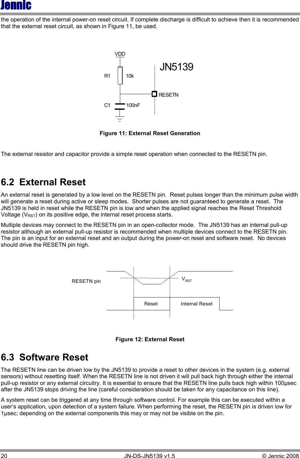
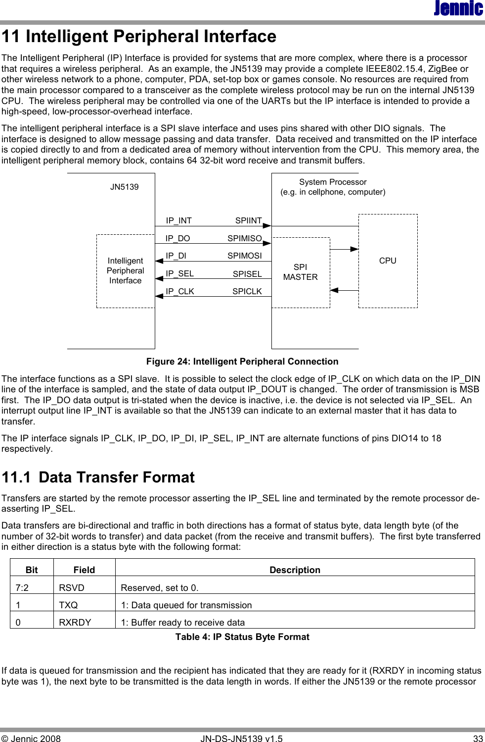
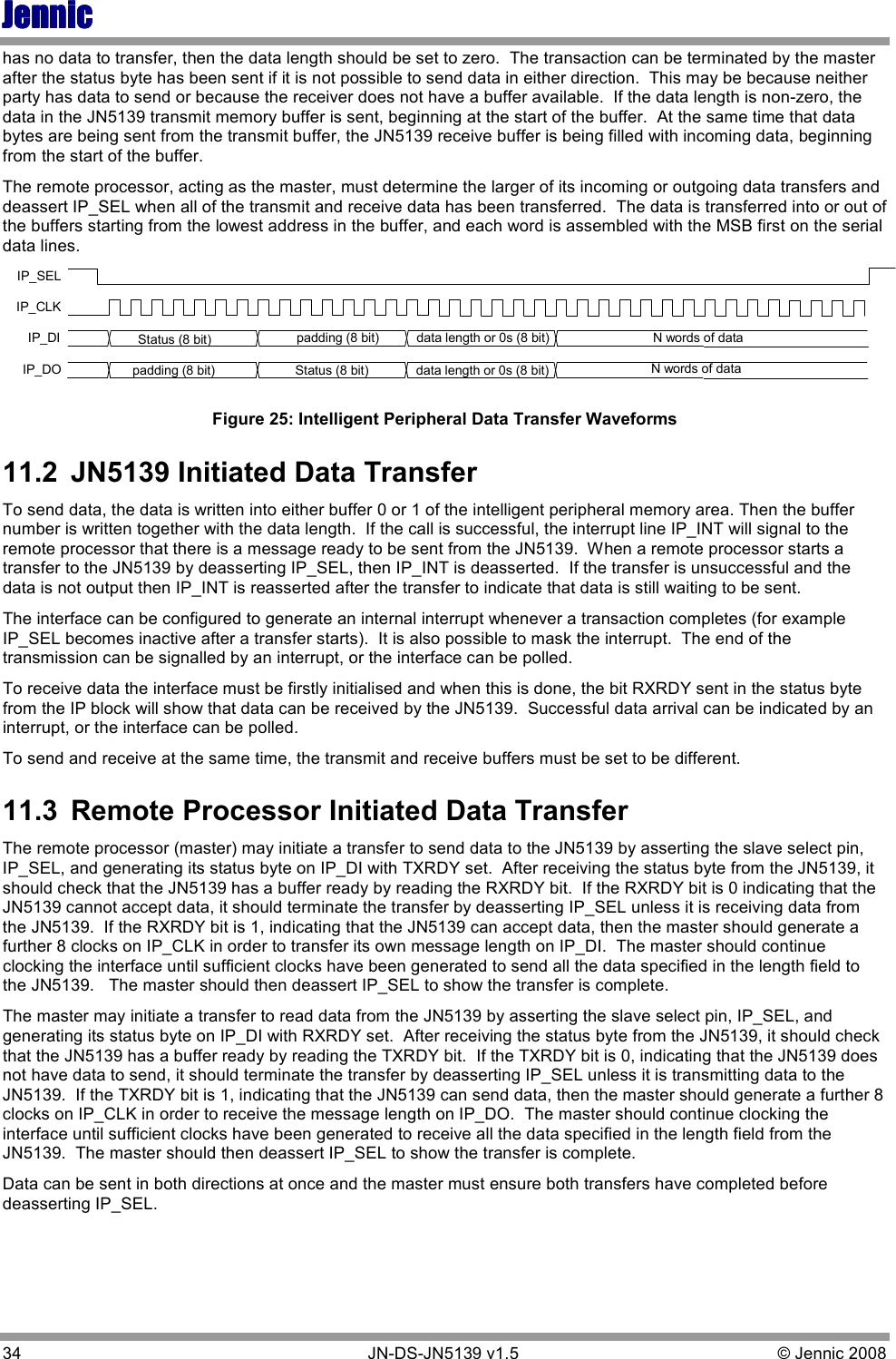
![JennicJennicJennicJennic © Jennic 2008 JN-DS-JN5139 v1.5 19 6 Reset A system reset initialises the device to a predefined state and forces the CPU to start program execution from the reset vector. The reset process that the JN5139 goes through is as follows. When power is applied, the 32kHz oscillator starts up and stabilises, which takes approximately 100µsec. At this point, the 16MHz crystal oscillator is enabled and power is applied to the processor and digital logic. The logic blocks are held in reset until the 16MHz crystal oscillator stabilises, which typically takes 2.5ms. Once the oscillator is up and running the internal reset is removed from the CPU and peripheral logic and the CPU starts to run code beginning at the reset vector, consisting of initialisation code and then optionally the resident Boot Loader (described in JN-AN-1003 Boot Loader Operation [2]). Section 17.3.1 provides detailed electrical data and timing. The JN5139 has three sources of reset: • Internal Power-on Reset • External Reset • Software Reset Note: When the device exits a reset condition, device operating parameters (voltage, frequency, temperature, etc.) must be met to ensure operation. If these conditions are not met, then the device must be held in reset until the operating conditions are met. (See section 17.3.1) 6.1 Internal Power-on Reset For the majority of applications the internal power-on reset is capable of generating the required reset signal. When power is applied to the device, the power-on reset circuit monitors the rise of the VDD supply. When VDD reaches the specified threshold, the reset signal is generated and can be observed as a rising edge on the RESETN pin. This signal is held internally until the power supply and oscillator stabilisation time has elapsed, at which point the internal reset signal is then removed and the CPU is allowed to run. RESETN PinInternal RESETVDD Figure 10: Internal Power-on Reset If the application requires a power supply reset to be used, i.e. removing and then applying VDD, it is important that the device decoupling capacitors are completely discharged before the VDD is re-applied. Failure to do so may inhibit](https://usermanual.wiki/NXP-Laboratories-UK/JN5139M4.manual/User-Guide-1094185-Page-19.png)
![JennicJennicJennicJennic 24 JN-DS-JN5139 v1.5 © Jennic 2008 8.1.1 Radio External components The VCO loop filter requires three external components and the IBIAS pin requires one external component as shown in Figure 15. These components should be placed close to the JN5139 pins and analogue ground. 15VCOTUNE3n3F330pF4k71% VB_VCO1943k1%VSSAIBIASVSSA100nF Figure 15: VCO Loop Filter and IBIAS The radio is powered from a number of internal 1.8V regulators fed from the analogue supply VDD1, in order to provide good noise isolation between the digital logic of the JN5139 and the analogue blocks. These regulators are also controlled by the baseband controller and protocol software to minimise power consumption. Decoupling for internal regulators is required as described in section 2.2.1, Power Supplies. 8.1.2 Antenna Diversity Support is provided for antenna diversity. Antenna diversity is a technique that maximises the performance of an antenna system. It allows the radio to switch between two antennas that have very low correlation between their received signals. Typically, this is achieved by spacing two antennas around 0.25 wavelengths apart or by using two orthogonal polarisations. So, if a packet is transmitted and no acknowledgement is received, the radio system can switch to the other antenna for the retry, with a different probability of success. The JN513x provides an output on DIO12 that is asserted on odd numbered retries that can be used to control an antenna switch; this enables antenna diversity to be implemented easily (see Figure 16 and Figure 17) Antenna AADO (DIO[12])Antenna BDevice RF PortRF Switch: Single-Pole, Double-Throw (SPDT)A BCOMSELSELB Figure 16 Simple Antenna Diversity Implementation using External RF Switch](https://usermanual.wiki/NXP-Laboratories-UK/JN5139M4.manual/User-Guide-1094185-Page-24.png)
![JennicJennicJennicJennic © Jennic 2008 JN-DS-JN5139 v1.5 25 TX ActiveADO (DIO[12])1stTX-RX Cycle 2ndTX-RX Cycle (1stRetry)RX Active Figure 17 Antenna Diversity ADO Signal for TX with Acknowledgement 8.2 Modem The Modem performs all the necessary modulation and spreading functions required for digital transmission and reception of data at 250kbps in the 2450MHz radio frequency band in compliance with the IEEE802.15.4 standard. AGC O-QPSKDemodulationSymbolDetection(Despreading)Pulse Shaping O-QPSKModulation SpreadingTXRXTX DataInterfaceRX DataInterfaceIQIIQQIF SignalGain Figure 18: Modem Architecture The transmitter receives symbols from the baseband processor and uses the spreading function to map each unique 4-bit symbol to a 32-chip Pseudo-random Noise (PN) sequence. Offset-QPSK modulation and half-sine pulse shaping is applied to the resultant spreading sequence to produce two independent quadrature phase signals (I and Q), which are subsequently converted to analogue voltages in the radio transmit path. The Automatic Gain Control (AGC) monitors the received signal level and adjusts the gain of the amplifiers in the radio receiver to ensure that the optimum signal amplitude is maintained during reception. The demodulator performs digital IF down-conversion and matched filtering and is extremely tolerant to carrier frequency offsets in excess of ±80ppm without suffering any significant degradation in performance.](https://usermanual.wiki/NXP-Laboratories-UK/JN5139M4.manual/User-Guide-1094185-Page-25.png)

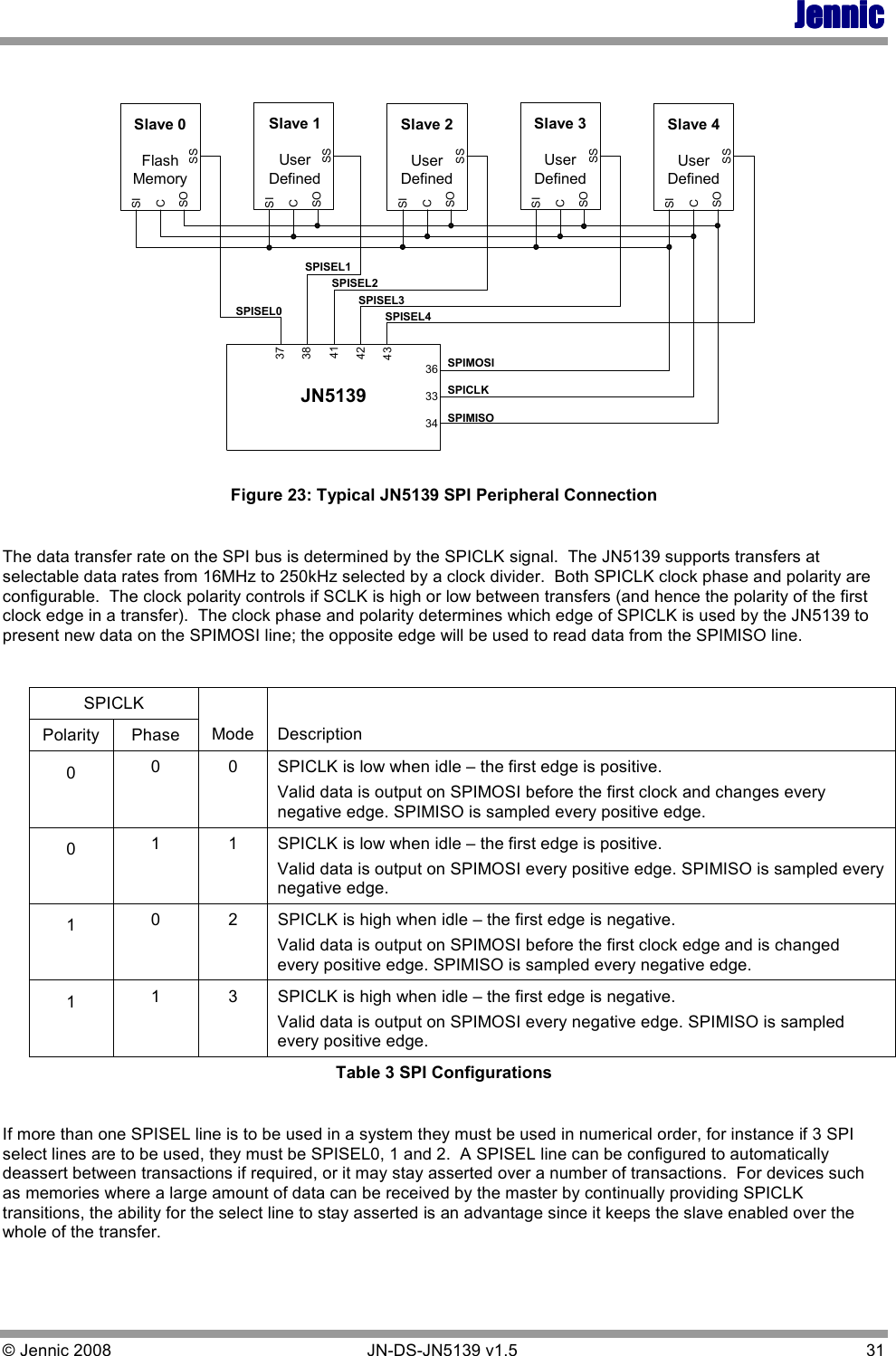
![JennicJennicJennicJennic 30 JN-DS-JN5139 v1.5 © Jennic 2008 10 Serial Peripheral Interface The Serial Peripheral Interface (SPI) allows high-speed synchronous data transfer between the JN5139 and peripheral devices. The JN5139 operates as a master on the SPI bus and all other devices connected to the SPI are expected to be slave devices under the control of the JN5139 CPU. The SPI includes the following features: • Full-duplex, three-wire synchronous data transfer • Programmable bit rates up to 16Mbps • Programmable transaction size of 8,16 or 32 bits • Supports standard SPI modes 0, 1, 2, 3 to allow control over the relationship between clock and transmit / receive data • Automatic slave select generation (up to 5 slaves) • Maskable transaction complete interrupt • LSB First or MSB First Data Transfer ClockDividerSPI BusCycleControllerData Buffer31 15 7DIVClock EdgeSelectDataCHAR_LENLSBSPIMISOSPIMOSISPICLKSelectLatchSPISEL [4..0]16 MHz0 Figure 22: SPI Block Diagram The SPI bus employs a simple shift register data transfer scheme. Data is clocked out of and into the active devices in a first-in, first-out fashion allowing SPI devices to transmit and receive data simultaneously. There are three dedicated pins SPICLK, SPIMOSI, SPIMISO that are shared across all devices on the bus. Master-Out-Slave-In or Master-In-Slave-Out data transfer is relative to the clock signal SPICLK generated by the JN5139. The JN5139 provides five slave selects, SPISEL0 to SPISEL4 to allow five SPI peripherals on the bus. SPISEL0 is a dedicated pin and SPISEL1 to 4, are alternate functions of pins DIO0 to 3 respectively. This allows a serial flash memory to be connected to SPISEL0 and download to internal RAM via software from reset. The interface can transfer 8, 16 or 32 bits without software intervention and can keep the slave select lines asserted between transfers when required, to enable longer transfers to be performed.](https://usermanual.wiki/NXP-Laboratories-UK/JN5139M4.manual/User-Guide-1094185-Page-30.png)


![JennicJennicJennicJennic © Jennic 2008 JN-DS-JN5139 v1.5 51 17.2.2 DC Current Consumption VDD = 2.2 to 3.6V, -40 to +85º C 17.2.2.1 Active Processing Mode: Min Typ Max Unit Notes CPU processing 2.85 + 0.295/MHz 4.5 + 0.480/MHz mA SPI, DIOs enabled Radio transmit [boost mode] 38 [42] 50 [55] mA CPU in software doze – radio transmitting Radio receive [boost mode] 37 [40] 48 [53] mA CPU in software doze – radio in receive mode The following current figures should be added to those above if the feature is being used ADC 655 µA Temperature sensor and battery measurements require ADC DAC 215 / 235 µA One / both Comparator 67.5 [1.2] µA Fast response time [low-power] UART 95 µA For each UART Timer 65 µA For each Timer 2-wire serial interface 75 µA 17.2.2.2 Sleep Mode Mode: Min Typ Max Unit Notes Sleep mode with I/O wakeup (Waiting on I/O event) 0.1 µA Sleep mode with I/O and timer wakeup – measured at 25ºC 1.2 2.5 µA As above but also waiting on timer event. If both wakeup timers are enabled then add another 0.3µA The following current figures should be added to those above if the feature is being used RAM retention – measured at 25ºC 2.4 10 µA For full 96kB retained. Comparator (low-power mode) 1.2 µA Reduced response time. 17.2.2.3 Deep Sleep Mode Mode: Min Typ Max Unit Notes Deep sleep mode – measured at 25ºC 60 250 nA Waiting on chip RESET or I/O event.](https://usermanual.wiki/NXP-Laboratories-UK/JN5139M4.manual/User-Guide-1094185-Page-51.png)
![JennicJennicJennicJennic 60 JN-DS-JN5139 v1.5 © Jennic 2008 17.3.12.1 Radio parameters: 2.2-3.6V, +25ºC Parameter Min Typical Max Unit Notes Receiver Characteristics Receive sensitivity -89 -96 dBm Nominal for 1% PER, as per 802.15.4 section 6.5.3.3 Receive sensitivity (boost) -91 -96.5 dBm Nominal for 1% PER, as per 802.15.4 section 6.5.3.3 Maximum input signal 0 dBm For 1% PER, measured as sensitivity Adjacent channel rejection -1 channel / +1 channel [CW Interferer] 31 / 35 [35 / 38] dB For 1% PER with wanted signal 3dB above sensitivity, as per 802.15.4 section 6.5.3.4 (modulated interferer) Alternate channel rejection [CW Interferer] 41 [45] dB For 1% PER with wanted signal 3dB above sensitivity, as per 802.15.4 section 6.5.3.4 (modulated interferer) Other in band rejection 2.4 to 2.4835 GHz, excluding adj channels 50 dB For 1% PER with wanted signal 3dB above sensitivity, measured as per 802.15.4 section 6.5.3.4 Out of band rejection 43 dB Spurious emissions (RX) -60 -53 -57 -47 dBm 30MHz to 1GHz 1GHz to 12GHz Intermodulation protection 50 dB For 1% PER at with wanted signal 3dB above sensitivity. Modulated Interferers at 2 & 4 channel separation RSSI linearity -4 +4 dB -95 to -10dBm Transmitter Characteristics Transmit power +1.5 dBm Transmit power (boost) 0 +2.7 dBm Output power control range -30.1 dB in 5 6dB steps Spurious emissions (TX) -59 -47 -36 -43 -47 dBm 30MHz to 1GHz, 1GHz to12.5GHz, The following exceptions apply 1.8 to 1.9GHz & 5.15 to 5.3GHz EVM [offset] 15 [4.5] 25 % At maximum output power Transmit Power Spectral Density -37 -20 dBc At greater than 3.5MHz offset, as per 802.15.4, section 6.5.3.1](https://usermanual.wiki/NXP-Laboratories-UK/JN5139M4.manual/User-Guide-1094185-Page-60.png)
![JennicJennicJennicJennic © Jennic 2008 JN-DS-JN5139 v1.5 61 17.3.12.2 Radio parameters: 2.2-3.6V, -40ºC Parameter Min Typical Max Unit Notes Receiver Characteristics Receive sensitivity -97 dBm Nominal for 1% PER, as per 802.15.4 section 6.5.3.3 Maximum input signal 0 dBm For 1% PER, measured as sensitivity Adjacent channel rejection -1 channel / +1 channel 31 / 35 dB For 1% PER with wanted signal 3dB above sensitivity, as per 802.15.4 section 6.5.3.4 Alternate channel rejection 42 dB For 1% PER with wanted signal 3dB above sensitivity, as per 802.15.4 section 6.5.3.4 Other in band rejection 40 dB 2.4 to 2.4835 GHz, excluding adjacent channels For 1% PER with wanted signal 3dB above sensitivity, measured as per 802.15.4 section 6.5.3.4 Out of band rejection 40 dB Spurious emissions (RX) -60 -53 -57 -47 dBm 30MHz to 1GHz 1 to 12GHz Intermodulation protection 50 dB For 1% PER at with wanted signal 3dB above sensitivity. Modulated Interferers at 2 & 4 channel separation RSSI linearity -4 +4 dB -95 to -10dBm Transmitter Characteristics Transmit power -1 +2 dBm Transmit power (boost) +3 dBm Output power control range -29.3 dB in 5 6dB steps Spurious emissions (TX) -59 -46 -36 -43 -47 dBm 30MHz to 1GHz, 1GHz to12.5GHz, The following exceptions apply 1.8 to 1.9GHz & 5.15 to 5.3GHz EVM [offset] 20 [6.2] 30 % At maximum output power Transmit Power Spectral Density -36 -20 dBc At greater than 3.5MHz offset, as per 802.15.4, section 6.5.3.1](https://usermanual.wiki/NXP-Laboratories-UK/JN5139M4.manual/User-Guide-1094185-Page-61.png)
![JennicJennicJennicJennic 62 JN-DS-JN5139 v1.5 © Jennic 2008 17.3.12.3 Radio parameters: 2.2-3.6V, +85ºC Parameter Min Typical Max Unit Notes Receiver Characteristics Receive sensitivity -94 dBm Nominal for 1% PER, as per 802.15.4 section 6.5.3.3 Maximum input signal 0 dBm For 1% PER, measured as sensitivity Adjacent channel rejection -1 channel / +1 channel 27 / 35 dB For 1% PER with wanted signal 3dB above sensitivity, as per 802.15.4 section 6.5.3.4 Alternate channel rejection 44 dB For 1% PER with wanted signal 3dB above sensitivity, as per 802.15.4 section 6.5.3.4 Other in band rejection 44 dB 2.4 to 2.4835 GHz, excluding adjacent channels For 1% PER with wanted signal 3dB above sensitivity, measured as per 802.15.4 section 6.5.3.4 Out of band rejection 44 dB Spurious emissions (RX) -60 -54 -57 -47 dBm 30MHz to 1GHz 1GHz to 12GHz Intermodulation protection 51 dB For 1% PER at with wanted signal 3dB above sensitivity. Modulated Interferers at 2 & 4 channel separation RSSI linearity -4 +4 dB -95 to -10dBm Transmitter Characteristics Transmit power -1.3 dBm Transmit power (boost) +0.6 dBm Output power control range -35 dB in 5 steps of 6dB Spurious emissions (TX) -59 -50 -36 -43 -47 dBm 30MHz to 1GHz, 1GHz to12.5GHz, The following exceptions apply 1.8 to 1.9GHz & 5.15 to 5.3GHz EVM [offset] 12 [3.6] 25 % At maximum output power Transmit Power Spectral Density -38 -20 dBc At greater than 3.5MHz offset, as per 802.15.4, section 6.5.3.1](https://usermanual.wiki/NXP-Laboratories-UK/JN5139M4.manual/User-Guide-1094185-Page-62.png)


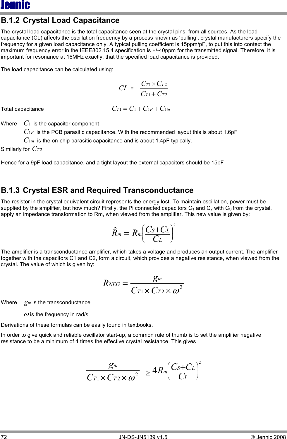
![JennicJennicJennicJennic © Jennic 2008 JN-DS-JN5139 v1.5 73 This can be used to give an equation for the required transconductance. 21221212])([4TTTTTTSmmCCCCCCCRg××++×≥ω Example: Using typical parameters of mR=40Ω, SC=1pF and 1TC=2TC=18pF ( for a load capacitance of 9pF), the equation above gives the required transconductance (mg) as 647uA/V. The JN5139 has a typical value for transconductance of 1.25mA/V The example and equation illustrate the trade-off that exists between the load capacitance and crystal ESR. For example, a crystal with a higher load capacitance can be used, but the value of max. ESR that can be tolerated is reduced. Also note, that the circuit sensitivity to external capacitance [ C1 , C2 ] is a square law. Below is measurement data showing the variation of the crystal oscillator amplifier transconductance with temperature and supply voltage, notice how small the variation is. Circuit techniques have been used to apply compensation, such that the user need only design for nominal conditions. Crystal Oscillator Transconductance Versus Temperature (VDD=3V)1.2451.251.2551.261.2651.271.2751.281.285-40 -20 0 20 40 60 80 100Temperature (C)Transconductance (mA/V) Crystal Oscillator Transconductance Versus Supply Voltage (Temp=25C)1.21.221.241.261.281.31.322.2 2.4 2.6 2.8 3.0 3.2 3.4 3.6Supply Voltage (VDD)Transconductance (mA/V)](https://usermanual.wiki/NXP-Laboratories-UK/JN5139M4.manual/User-Guide-1094185-Page-73.png)

![JennicJennicJennicJennic © Jennic 2008 JN-DS-JN5139 v1.5 83 Appendix C Related Documents [1] IEEE Std 802.15.4-2003 IEEE Standard for Information technology – Part 15.4 Wireless Medium Access Control (MAC) and Physical Layer (PHY) Specifications for Low-Rate Wireless Personal Area Networks (LR-WPANs) [2] JN-AN-1003 Boot Loader Operation [3] JN-AN-1062 Using OTP eFuse Memory [4] JN-AN-1038 Programming Flash devices not supported by the JN51xx ROM-based bootloader RoHS Compliance JN5139 devices meet the requirements of Directive 2002/95/EC of the European Parliament and of the Council on the Restriction of Hazardous Substance (RoHS). Status Information The status of this Data Sheet is Production. Jennic products progress according to the following format: Advanced The Data Sheet shows the specification of a product in planning or in development. The functionality and electrical performance specifications are target values and may be used as a guide to the final specification. Integrated circuits are identified with an R suffix, for example JN5139-Z01R. Jennic reserves the right to make changes to the product specification at anytime without notice. Preliminary The Data Sheet shows the specification of a product that is in production, but is not yet fully qualified. The functionality of the product is final. The electrical performance specifications are target values and may used as a guide to the final specification. Integrated circuits are identified with an R suffix, for example JN5139-Z01R. Jennic reserves the right to make changes to the product specification at anytime without notice. Production This is the final Data Sheet for the product; all product characterization is completed. All functional and electrical performance specifications where included, including min and max values are final. This Data Sheet supersedes all previous document versions. Jennic reserves the right to make changes to the product specification at anytime to improve its performance.](https://usermanual.wiki/NXP-Laboratories-UK/JN5139M4.manual/User-Guide-1094185-Page-83.png)