Motorola Mobility T56LV1 Cellular/ PCS WCDMA/ GSM/ EDGE Data Transceiver - HTM1100-L User Manual APPLICANT MOTOROLA INC

Motorola Mobility LLC Cellular/ PCS WCDMA/ GSM/ EDGE Data Transceiver - HTM1100-L APPLICANT MOTOROLA INC

Contents

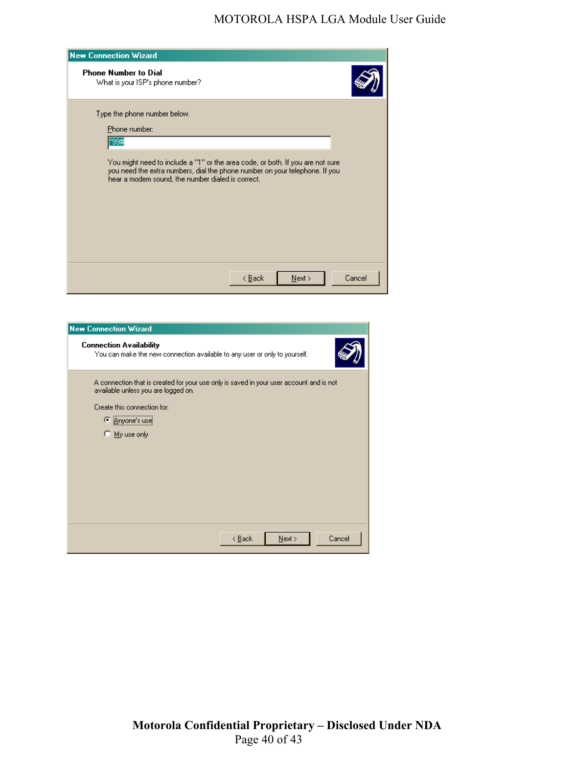
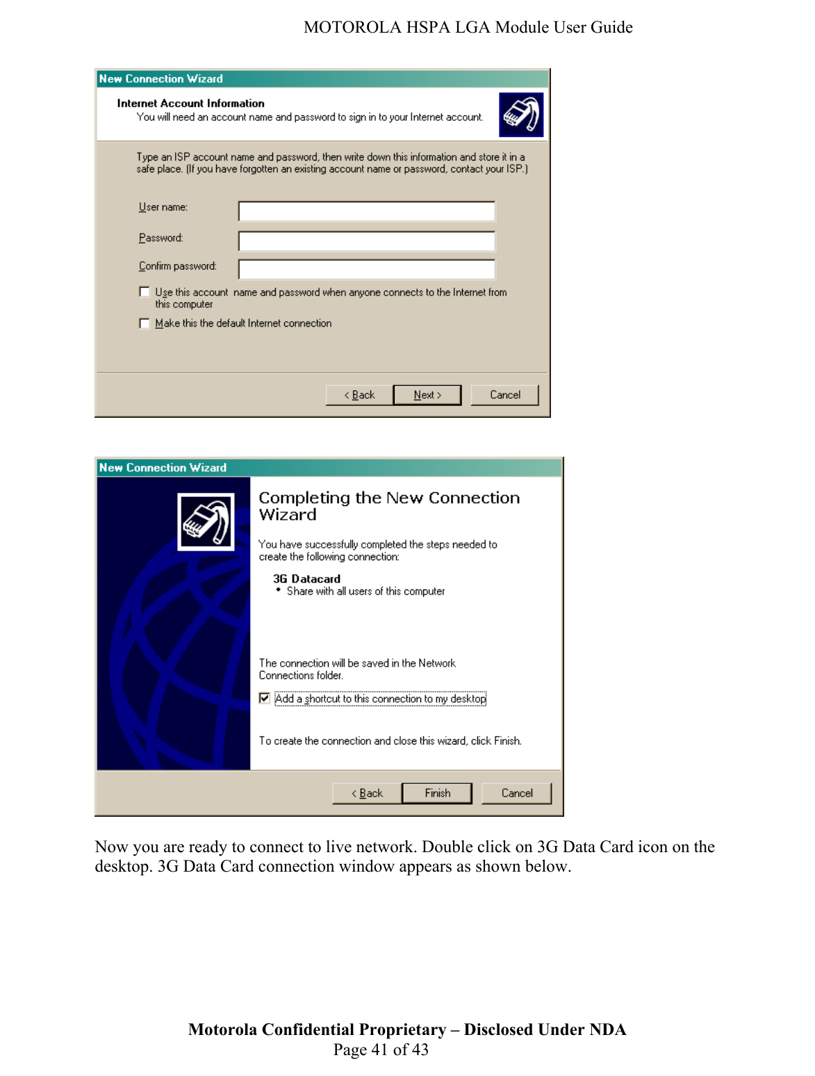
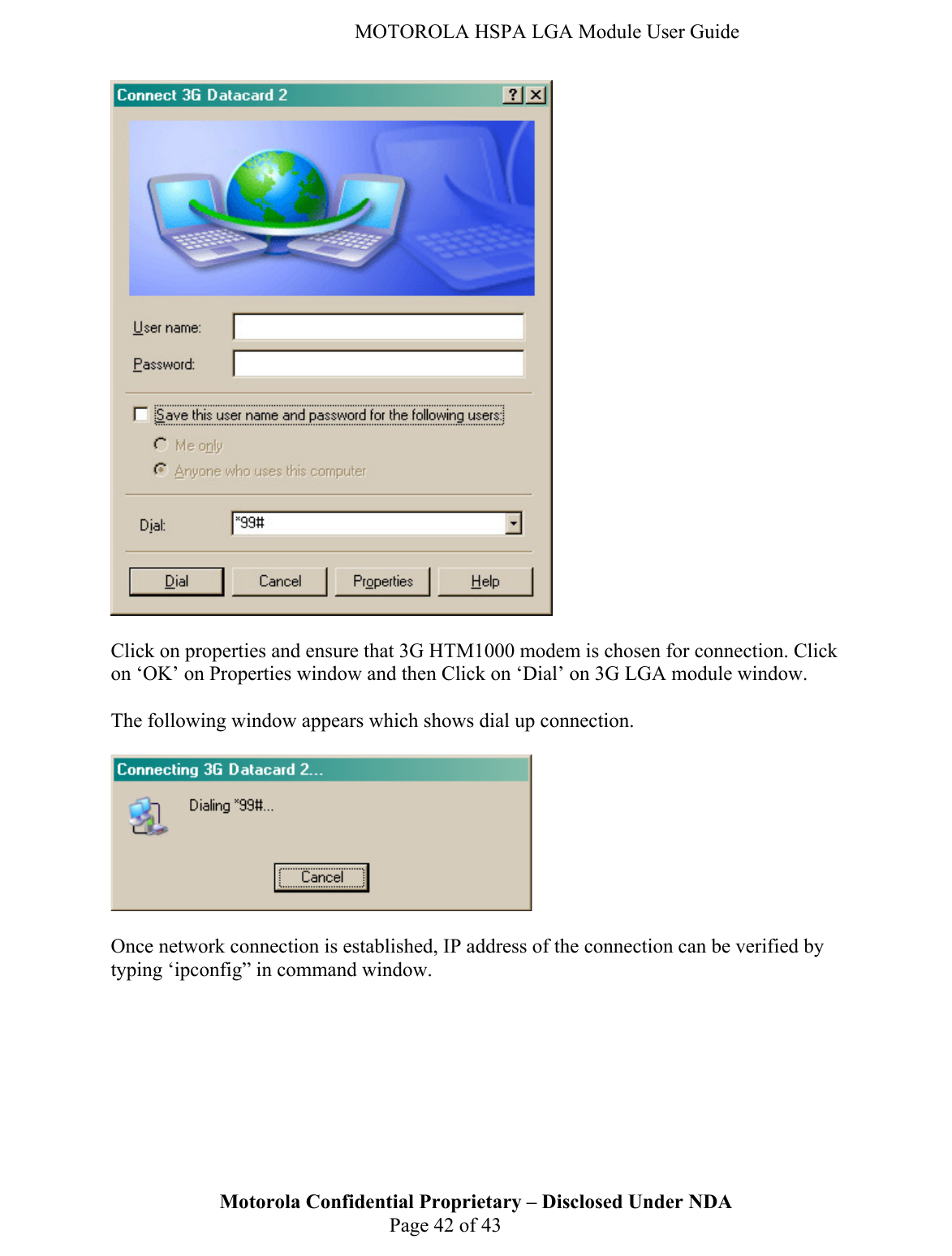
Exhibit 8 Users Manual

APPLICANT MOTOROLA INC.                                              FCC ID: IHDT56LV1   INSTRUCTION MANUAL  A representative version of the user's manual follows: Exhibit 8
  MOTOROLA HSPA LGA Module User Guide       HSPA LGA module (HTM1100-L) User Guide           DOCUMENT CONTROL NUMBER:   Version No.:  1.0  Date: March 2010    Motorola Confidential Proprietary – Disclosed Under NDA  Page 1 of 43 Copyright 2010 Motorola Inc.  All rights reserved.  This document and the information contained in it is CONFIDENTIAL INFORMATION of Motorola, and shall not be used, published, disclosed, or disseminated outside of Motorola in whole or in part without Motorola’s consent. This document contains trade secrets of Motorola. Copyright notice does not imply publication of this document.
  MOTOROLA HSPA LGA Module User Guide  HSPA LGA MODULE (HTM1100-L)........................................................................................................ 1 USER GUIDE ............................................................................................................................................... 1 1. INTRODUCTION............................................................................................................................... 4 1.1 REVISION HISTORY ...................................................................................................................... 4 1.2 PURPOSE ...................................................................................................................................... 4 1.3 SCOPE .......................................................................................................................................... 4 1.4 TARGET AUDIENCE ...................................................................................................................... 4 1.5 ABBREVIATIONS........................................................................................................................... 5 2. REFERENCES.................................................................................................................................... 6 3. PRODUCT OVERVIEW ................................................................................................................... 7 4. HARDWARE ARCHITECTURE..................................................................................................... 8 5. SOFTWARE ARCHITECTURE ...................................................................................................... 9 5.1.1 Inter-Processor Communication........................................................................................... 10 5.1.2 Modem Software Architecture Overview .............................................................................. 10 5.1.3 ARM9 Software Architecture Overview................................................................................ 11 6. HTM1100-L MODULE FEATURE SUMMARY .......................................................................... 12 6.1 HARDWARE REVISION:............................................................................................................... 12 6.2 2G.............................................................................................................................................. 12 6.3 3G.............................................................................................................................................. 12 6.4 ADVANCED SERVICES ................................................................................................................ 12 6.5 AUDIO ........................................................................................................................................ 12 6.6 INTERNAL MEMORY................................................................................................................... 13 6.7 SYSTEM REQUIREMENTS ............................................................................................................ 13 6.8 SECURITY................................................................................................................................... 13 6.9 CONNECTIVITY........................................................................................................................... 13 6.10 POWER UP SEQUENCE ................................................................................................................ 13 7. SPECIFICATIONS........................................................................................................................... 15 7.1.1 Electrical Specification......................................................................................................... 15 7.1.2 Mechanical Specification...................................................................................................... 15 8. LGA MODULE INTERFACES ...................................................................................................... 17 8.1.1 LGA Interface Signals .......................................................................................................... 17 8.1.2 SIM Interface ........................................................................................................................ 20 8.1.3 WWAN_LED......................................................................................................................... 20 8.1.4 Audio Interface ..................................................................................................................... 20 9. COMMUNICATION WITH HOST ............................................................................................... 21 9.1.1 Overview............................................................................................................................... 21 9.1.2 Link Details .......................................................................................................................... 22 9.1.3 Host Modem Wakeup Mechanism......................................................................................... 23 10. AT COMMANDS......................................................................................................................... 25 10.1 LGA MODULE AT COMMAND INTERFACE ALLOWS THE BELOW MENTIONED FUNCTIONALITY ON HIGH LEVEL USING DIFFERENT AT COMMANDS:....................................................................................... 25 10.1.1 Network Connection Management................................................................................... 25 10.1.2 Registration or Mobility Management............................................................................. 26 10.1.3 SMS.................................................................................................................................. 26 Motorola Confidential Proprietary – Disclosed Under NDA  Page 2 of 43 10.1.4 USIM and Phonebook ...................................................................................................... 26
  MOTOROLA HSPA LGA Module User Guide 11. NVM/FLASH................................................................................................................................27 12. RF CALIBRATION/PHASING.................................................................................................. 27 13. PLATFORM VALIDATION ...................................................................................................... 28 13.1 RF PERFORMANCE TESTING....................................................................................................... 28 13.1.1 Equipment ........................................................................................................................ 28 13.1.2 Equipment list .................................................................................................................. 28 13.1.3 Setup ................................................................................................................................29 14. HARDWARE INSTALLATION ................................................................................................ 30 14.1 HTM1100 LGA MODULE REFLOW PROCESS ............................................................................. 30 15. LGA MODULE DRIVER INSTALLATION............................................................................ 32 16. LIVE NETWORK CONNECTION ........................................................................................... 35 16.1 PLUGGING IN THE CARD IN PC.................................................................................................... 35 16.2 SETTING UP DIAL UP NETWORKING (DUN) CONNECTION USING LGA MODULE AS A MODEM.. 35 17. KNOWN ISSUES......................................................................................................................... 43 17.1 LGA MODULE POWER UP TIMING.............................................................................................. 43  Figure 1: HTM1100-L Bottom Pad view............................................................................ 7 Figure 2: HTM1100 high level block diagram ................................................................... 8 Figure 3: Software Architecture Partitioning...................................................................... 9 Figure 4: Power Management by CPCAP ........................................................................ 14 Figure 5: HTM1100-L Component View and Pad View (Top View).............................. 16 Figure 6: Communication between Host and LGA Module............................................. 21 Figure 7: HTM1100-L Modem interface.......................................................................... 22 Figure 8: GPIO remote wakeup signaling ........................................................................ 24 Figure 9: LGA Module test set up .................................................................................... 28 Figure 10 : LGA module inside Test Socket .................................................................... 31 Motorola Confidential Proprietary – Disclosed Under NDA  Page 3 of 43
  MOTOROLA HSPA LGA Module User Guide  1. Introduction 1.1  Revision History   Revision Date Author Description 1.0 March 2010 Customer Operations – Lauren Holmes (GTJM87) Initial Draft        1.2  Purpose  This document describes the product design and specification for HSPA LGA module (HTM1100-L). The HTM1100-L supports multi-mode (2G/3G) with HSDPA/HSUPA capabilities.  1.3  Scope This document describes platform architecture, hardware/software interactions, Technical/Electrical Specifications. Motorola Confidential Proprietary – Disclosed Under NDA  Page 4 of 43 1.4  Target Audience This document is intended to provide design details about HSPA LGA module (HTM1100-L) to the teams involved in product integration.
  MOTOROLA HSPA LGA Module User Guide Motorola Confidential Proprietary – Disclosed Under NDA  Page 5 of 43 1.5  Abbreviations AES    Advanced Encryption Standard AGPS    Assisted Global Positioning System AMR-NB  Adaptive Multi-Rate Narrow Band AMR-WB  Adaptive Multi-Rate Wide Band AP   Applications Processor BP   Baseband Processor DES    Data Encryption Standard DDR    Double Data Rate DTM    Dual Transfer Mode DUN    Dial Up Networking EDGE    Enhanced Data rate for GSM Evolution EFR    Enhanced Full Rate FPS   Frames-Per-Second FR   Full Rate GEA    GSM Encryption Algorithm GPRS    General Packet Radio Service GPS    Global Positioning System GSM    Global System for Mobile communications HR   Half Rate HS   High Speed HSDPA    High-Speed Downlink Packet Access HSUPA    High-Speed Uplink Packet Access IMEI    International Mobile Equipment Identity IMS    IP Multimedia Subsystems IPC    Inter Processor Communications LGA    Land Grid Array NAND    Not AND (electronic logic gate) OHA    Open Handset Alliance OMA    Open Mobile Alliance OTG   On-The-Go PCI    Peripheral Component Interconnect PMIC    Power Management IC RF   Radio Frequency SAM    Stand Alone Modem SDRAM   Synchronous Dynamic Random Access Memory SIM    Subscriber Identity Module UEA    UMTS Encryption Algorithm UICC    Universal Integrated Circuit Card USB    Universal Serial Bus USIM   Universal SIM W3G    Wrigley3G (Motorola 3G baseband processor) WCDMA  Wideband Code Division Multiple Access WLAN    Wireless Local Area Network WWAN    Wireless Wide Area Network
  MOTOROLA HSPA LGA Module User Guide 2. References HTM1100-L is compliant with 3GPP specification Release6, December 2006 version.  Release 6 specifications can be found at www.3gpp.org  HTM1100-L pads comply with electrical specifications of PCIe Express specification 1.2. PCIe Express specification 1.2 can be downloaded from http://www.pcisig.com/specifications/pciexpress/  HTM1100-L USB signals and remote host wake up mechanism comply with USB specification 2.0. USB2.0 specification can be downloaded from http://www.usb.org/developers/docs/  JEDEC standards: http://www.jedec.org/ ESD protection is in compliance with JESD22-A114. Moisture sensitivity level complies with Ref J-STD-020B section 7. Reflow process is in compliant with J-STD-020C.  Linux source code drivers for HTM1100-L product are available at http://opensource.motorola.com  Host Modem communication details are provided in the document HTM1100-L Host Modem Communication 12-17-09 Ver 1-0-1.pdf     Motorola Confidential Proprietary – Disclosed Under NDA  Page 6 of 43
  MOTOROLA HSPA LGA Module User Guide 3. Product Overview  HTM1100-L is a LGA module supporting tri-band HSPA and quad-band EDGE/GPRS, with data rates of up to 10.1Mbps downlink and 5.76Mbps uplink.  Signals on LGA module comply with Electrical spec of PCIe interface Version 1.2.  HTM1100-L is based on a custom 3G baseband processor that was developed by Motorola. Other main hardware components on this platform are the RF transceiver from Infineon, the Power Management IC, the RF analog front end and Power amplifiers. HTM1100-L has internal DDR SDRAM and NAND flash memories, which were packaged on top of the baseband processor (POP). HTM1100-L uses USB signals to connect with a PC, netbook or MID.          HTM1100-L Bottom View         HTM1100-L Bottom view  (Engineering Sample)    (Production version)  Figure 1: HTM1100-L Bottom Pad view Motorola Confidential Proprietary – Disclosed Under NDA  Page 7 of 43 J I H G F E D C B A J I H G F E D C B A 987654321987654321
  MOTOROLA HSPA LGA Module User Guide  4. Hardware Architecture      Figure 2: HTM1100 high level block diagram Motorola Confidential Proprietary – Disclosed Under NDA  Page 8 of 43 .
  MOTOROLA HSPA LGA Module User Guide  5. Software Architecture The HTM1100-L module software architecture is based on: • Linux kernel running on the ARM9 application processor of the W3G. • Native services running on top of the Linux kernel in the user space. • Hardware specific adapters, drivers and software stacks. • A 3GSM Single Core Modem architecture running on the C55x+ DSP of the W3G. The following diagram shows a high level overview of the software partitioning:  Figure 3: Software Architecture Partitioning  The ARM9 in W3G hosts Linux kernel and some native services that are running in the user space. The external peripherals that the LGA module supports are limited to UICC and  PCI Express connector which includes USB connectivity lines. The internal peripherals that W3G supports are limited to DDR SDRAM and NAND Flash memories, the RF transceiver SmartiUEMD from Infineon and the CPCAP power management IC. Motorola Confidential Proprietary – Disclosed Under NDA  Page 9 of 43 W 3 GCPCAP POWER ICNAND FLASHDDR SDRAMSIM IF SmartiUEMD RFULPIHSUSB OTGSDRCC55 +x RF IFUICC2G/3G StackARM9Android KernelGPMCGPIOUSBXVRUSB_D+USB_D-Native ServicesLGA  I NTE R F ACE
  MOTOROLA HSPA LGA Module User Guide 5.1.1 Inter-Processor Communication The Inter-Processor Communication (IPC) infrastructure between the Single Core Modem and Application Subsystem is made up of a shared RAM between the ARM9 and the C55x+, and a mailbox mechanism, on top of which the NetMux software infrastructure exposes virtual channels to client components on both Application (AP) and Baseband Processor (BP) sides. 5.1.2 Modem Software Architecture Overview In this platform, the W3G processor includes a C55x+ DSP that runs the whole 2G/3G modem stack (supporting HSDPA/HSUPA) thus leaving the ARM9 fully dedicated to native services.  This approach enables native services to run on the application processor without the complexity of mixing hard real-time software (modem) with the applications. The SCM architecture enables running all the modem functions: 2G and 3G Signal Processing Layer (SPL) and 2G Stack and 3G stack on the SAM core (C55x+ core). Only what is needed to support modem functions is implemented on the C55x+ DSP core. Interfaces have been split into 3 main domains: SPL, Stack and Infrastructure. The Single Core Modem Software architecture is composed of the following elements: • The Signal Processing Layer (SPL): this software layer implements the physical layer. o Uplink signal processing: channel coding and modulation, GSM convolutional encoding and WCDMA convolutional encoding or Turbo-encoding. o Downlink signal processing: GSM equalization, GSM channel decoding, WCDMA interface/control and WCDMA hardware accelerators (3G Sub-System). • Stack component is the component from L1 Control to L3 handling all the logical part of the GSM/GPRS/EGPRS and WCDMA protocols: o GSM/GPRS/EDGE protocols: Layer 1, Layer2-Link Access Protocol on the Dm channel (L2-LAPDm), GPRS Radio Link Control (RLC), Logical Link Control (LLC) and the Sub-Network Dependent Convergence Protocol (SNDCP).  Motorola Confidential Proprietary – Disclosed Under NDA  Page 10 of 43
  MOTOROLA HSPA LGA Module User Guide o WCDMA protocols: WCDMA Layer 1, Radio Resource Control (RRC), WCDMA Radio Link Control (W-RLC), Broadcast Message Control (BMC) and the Packet Data Convergence Protocol (PDCP). o Dual Mode protocols: Layer 1, GPRS Radio Resource/Radio Resource management (GRR/RR/RRC/RRLP), Mobility Management (MM), GPRS Mobility Manager (GMM), Session Management (SM), Intelligent Data Router (IDR) and Connection Management (CM), which consists of Call Control (CC), Supplementary Services (SS) and Short Message Management (SMS) entities. A new created entity is the Translation Layer (TL) which allows the 2G/WCDMA Engine Layer to interface with the AP (especially L3/L4 interface). The Infrastructure: this is the component providing the low-level mechanisms required by other SCM entities (Stack, SPL, IPC, AGPS and Audio control). It contains hardware drivers required by the others components like interrupt, watchdog, GPIO, and also entities for communicating with the application processor (IPC). Finally, it contains modules to relay functions to the application processor like NVM proxy, SIM proxy and Audio Proxy.  Motorola Confidential Proprietary – Disclosed Under NDA  Page 11 of 43 5.1.3 ARM9 Software Architecture Overview The Application Software Architecture uses the MotoAndroid architecture. The Android Linux kernel is made of the Linux Kernel with some additional patches including alarm, ashmem, binder, power management, low memory killer, kernel debugger, and logger. The Linux kernel version is 2.6.27 and includes several improvements made by OHA to the reference release in kernel.org. The layers provide a view in which system functionality is increasingly abstracted from hardware at the bottom layer, towards user functionality at the top layer. The Linux kernel provides the operating system kernel services. It separates all higher layers from the device hardware. Android relies on Linux version 2.6.27 for core system services such as security, memory management, process management, network stack, and driver model. The kernel also acts as an abstraction layer between the hardware and the rest of the software stack.
  MOTOROLA HSPA LGA Module User Guide  6. HTM1100-L Module Feature Summary Key capabilities of the LGA module and associated features of the platform are listed below. The following summary describes some of the platform capabilities. 6.1  Hardware Revision:  6.2  2G  • 3GPP Release 6 December 2006 version compliant  • Quad-band GSM 850/900/1800/1900 MHz • GPRS Class 12 • EDGE Class 12 • A5/1-3 (unused because no voice) and GEA/1-3 Encryption • DARP (Downlink Advanced Receiver Performance) • 2G to 3G handoffs based on 3GPP specification • Sensitivity (2% BER in voice call): less than -106dBm (-108dBm typical) • GPRS/EDGE Tx Output power(GMSK): Power Class 4, 33dBm(850 and 900Mhz) and Power Class1, 30dBm(1800MHz and 1900MHz) • EDGE Tx Power (8-PSK): Power class E2 (27dBm in 850/900 MHz and 26dBm in 1800/1900 MHz) 6.3  3G  • 3GPP Release 6 December 2006 version compliant,  • Frequency Bands o 850/1900/2100 MHz (Supported) • WCDMA 384kbps uplink (UL) – 384kbps downlink (DL) • HSDPA 7.2 / 10.1 Mbps • HSUPA 1.46 / 2 / 5.76 Mbps • UEA01, UEA02, UIA1, UIA2 Encryption • 3G Rx Diversity in all bands • 3G to 2G handoffs based on 3GPP specification • Sensitivity (0.1% BER in 12.2k voice call): less than -108dBm (-110dBm typical) • Output Power 23dBm 6.4  Advanced Services • GPS is not supported. 6.5  Audio • PCM signals are available on the LGA module Motorola Confidential Proprietary – Disclosed Under NDA  Page 12 of 43 • The master Clock is provided by LGA module. Support for Slave Clock will be available upon request
  MOTOROLA HSPA LGA Module User Guide • Supports PCM data formats: Word (16-bit) and 4 slots network mode • Mode 1 will be supported in initial release, Mode 2 is in development (see section 7.1.3.1) 6.6  Internal Memory • 64MByte NAND Flash Memory  • 32MByte DDR-333 166 MHz clock SDRAM  6.7  System Requirements • Linux Android Kernel (2.6.27) in the ARM9 of the W3G • VTRXmc in the C55x+ of the W3G 6.8  Security • High Assurance Boot with Multiple Super Root Key Support • MD5, SHA-1, SHA-256, 3DES, AES 128, RC4, RSA • Subsidy Lock • IMEI Protection 6.9  Connectivity • SIM or UICC (SIM and USIM) • USB client 2.0 HS Support (PC connectivity) • 3GDigRF RF interface version 3.07 6.10  Power Up Sequence The main power management function is performed by Power management IC (CPCAP), which receives an input voltage of 3.3V.  CPCAP is capable of accepting input voltage in the range of 3V to 4.5V. This input voltage range is being tested on LGA module.  CPCAP manages all the power requirements on module; it includes 2 bucks, 1 boost and 8 linear regulators.  Motorola Confidential Proprietary – Disclosed Under NDA  Page 13 of 43
  MOTOROLA HSPA LGA Module User Guide     Motorola Confidential Proprietary – Disclosed Under NDA  Page 14 of 43 Figure 4: Power Management by CPCAP
  MOTOROLA HSPA LGA Module User Guide 7. Specifications 7.1.1 Electrical Specification The HTM1100-L supports input voltage range of 3.0V to 4.2V supply. The module may power down if the input voltage range drops below 2.9V.  Following table shows the power consumption of HTM1100-L.  These measurements are based on 00.16.01I software. Mode Average Current at 3.3V  (mA) Power Consumption  (mW) EDGE Downlink FTP Transfer 200kbps 185 610 HSDPA 10.1Mbps/ Power level: 0dBm 412 1360 2G Voice Call in PCL 5 DTX (50%) 200 660 3G Voice Call 7dBm 260 858 Idle Mode in EDGE (DRX2), no CM 4.6 <20 Idle mode in WCDMA (K=7), no CM 4.2 <20 Airplane mode(RF off), no CM 3.3 <10  7.1.2 Mechanical Specification Physical dimensions of the card are: 29.3mm x 30.9mm Height of the module with shield is 2.7mm (including label, label =0.1mm). Weight of the module is ~6.1grams.  LGA module pad view as seen from the top is shown below. The actual bottom view of the pads is shown in section 2. Motorola Confidential Proprietary – Disclosed Under NDA  Page 15 of 43
  MOTOROLA HSPA LGA Module User Guide     Figure 5: HTM1100-L Component View and Pad View (Top View)  Motorola Confidential Proprietary – Disclosed Under NDA  Page 16 of 43
  MOTOROLA HSPA LGA Module User Guide 8. LGA module Interfaces 8.1.1 LGA Interface Signals The HTM1100-L connects with netbook, notebook or MID using LGA module interface signals. HTM1100-L uses USB interface on the module to connect with netbook, notebook or MID. Electrically the module will be seen as a USB device since it uses a standard USB2.0 connection. Power is supplied by motherboard. A SIM card must be provided by PC manufacturer for user authentication.  A Radio disable (W_Disable) signal is connected from PC to the card; this allows the user to enable/disable RF activity (Airplane mode) with a hardware switch. The module controls one of the PC’s LEDs to indicate RF activity has been disabled or enabled. This is driven by the signal LED_WWAN_B.  To summarize main characteristics of LGA Module: • Standard USB interface  • B+ (3.0V to 4.2V) power supply from motherboard is used. Filter caps must be added on these lines based on the PCB design.  • Expected max current in worst case scenario (with VSWR = 4) is around 1.1A averaged over 1sec, 2.75A averaged over 100µs.  • W_DISABLE is used to enable/disable RF activity: 30s to disable, 1s to enable. • PC WWAN LED is controlled by the module.  The following table shows signals on LGA interface. The I/O level of all the pins is 1.8V.  Motorola Confidential Proprietary – Disclosed Under NDA  Page 17 of 43 Pin #  Pin Name   Direction  Pin Description A1 Ground   Ground A2 Ground   Ground A5 Ground   Ground A6 Ground   Ground A7 Ground   Ground A8 Ground   Ground A9 Ground   Ground B1 Ground   Ground B2 Ground   Ground B3 USB_DM Input / Output  USB 2.0 DM pin 100 ohms matched impedance B4 USB_DP Input / Output  USB 2.0 DP pin 100 ohms matched impedance B5 VSIMCARD  Output  SIM card power.3.0V/1.8V supported. B6 MICR_IN  Input  Mic input B7 MICR_GND   Mic ground pin B8 Ground   Ground B9 Ground   Ground C1 Ground   Ground
  MOTOROLA HSPA LGA Module User Guide Motorola Confidential Proprietary – Disclosed Under NDA  Page 18 of 43 C2 B+ Input  3.3V module  power.Max power <1.5W (550mA).Add filter caps. 10K PullDown needed for correct power up. C3 B+ Input  3.3V module  power.Max power <1.5W (550mA).Add filter caps C4 ON2B Input  System Power on pin. Has an internal PullUp. If functionality is unused, the pin can be left unconnected.  If functionality is used: - pin should be high at boot - if device was previously powered OFF by assertion of WATCHDOG_B a falling edge on ON2B will power ON the device. See section 7.1.5 for external circuit requirement. C5 LED_WWAN_B Output  Signal to control a system LED/icon; L= RF inactive.  This signal shall be capable of sinking to ground a minimum of 9.0mA at up to a maximum VOL of 400mV. C6 MICR_RB  Output  Mic bias C7 Ground   Ground C8 ANT_MAIN RF Input/Output Connect to antenna 50 ohms impedance. External matching circuit is required. See section 7.1.4 D1 Ground   Ground D2 NC (Not Connected)  This pin can be left unconnected.  D3 WATCHDOG_B Input  Watchdog interrupt, has an internal PullUp. If driven by Host:  - must be high at boot - can generate a Power OFF on falling edge See section 7.1.5 for external circuit D4 SYS_RESTART Input  Do not Use (Debug interface). This pin has internal PullUp. D5 LINE_OUT_R  Output  Audio line output D6 EAR_SPP  Output  Audio speaker output D7 Ground   Ground D8 Ground   Ground D9 Ground   Ground E1 Ground   Ground E2 HOST_WAKE Input / Output GPIO9 Open drain active low signal to wake up host. This pin has internal PullUp. Connect to a GPIO on host apps processor or leave it un connected if not used. E3 PCM_IN  Input  PCM input E4 Ground   Ground E5 Ground   Ground E6 EAR_SPM  Output  Audio speaker output E7 Ground   Ground E8 Ground   Ground E9 Ground   Ground F1 Ground   Ground F2 WAN_USB_EN Input /  GPIO8(LED_WLAN). This is still under
  MOTOROLA HSPA LGA Module User Guide Motorola Confidential Proprietary – Disclosed Under NDA  Page 19 of 43 Output  definition, can be connected to a GPIO on host apps processor or left un connected. F3 W_DISABLE Input / Output GPIO10(signal from baseband; active low =disable RF) F4 JTAG_RTCK  Output  Do not Use (Debug interface) F5 JTAG_TCK  Input  Do not Use (Debug interface) F6 JTAG_EMU0 Input / Output  Do not Use (Debug interface) F7 Ground   Ground F8 Ground   Ground F9 Ground   Ground G1 Ground   Ground G2 COEX1 Input / Output GPIO6 to coexist with other RF systems. Can be left un connected. G3 PCM_FSX Input / Output  PCM Frame sync G4 JTAG_TDO  Output  Do not Use (Debug interface) G5 JTAG_NTRST  Input  Do not Use (Debug interface) G6 JTAG_TMS  Input  Do not Use (Debug interface) G7 Ground   Ground G8 ANT_DIV RF Input  Receive diversity antenna. Connect to antenna 50ohm impedance.  External matching circuit is required. See section 7.1.4 H1 Ground   Ground H2 GPS_TIMESTAMP Output  CLK_REQ active low signal requesting for System clock/GPS time stamp. This is not supported in SW, can be left unconnected. H3 UART_RX  Input  Do not Use.  (UART transmit ) H4 PCM_CLKX Input / Output  PCM clock H5 COEX2 Output  SYS_CLKOUT2 output clk from W3G to coexist with other RF systems. Not supported in SW. Can be left unconnected. H6 PCM_OUT  Output  PCM output H7 Ground   Ground H8 Ground   Ground H9 Ground   Ground J1 Ground   Ground J2 Ground   Ground J3 UART_TX  Output  Do not Use.  (UART transmit )  J4 SIM_IO Input / Output SIM interface data IO. This pin has an internal PullUp. J5 SIM_CLK  Output  SIM clock, This pin has an internal PullUp J6 SIM_RST  Output  SIM reset. This pin has an internal PullUp J7 Ground   Ground J8  Ground   Ground J9  Ground   Ground K1 Ground   Ground K2 Ground   Ground K3 UART3_RX  Input  Do not Use (Debug interface) K4 UART3_TX  Output  Do not Use (Debug interface)
  MOTOROLA HSPA LGA Module User Guide K5 JTAG_EMU1 Input / Output  Do not Use (Debug interface) K6 JTAG_TDI  Input  Do not Use (Debug interface) K7 Ground   Ground K8 Ground   Ground K9 Ground   Ground Table 1 – HTM1100 LGA module connector pin out 8.1.2 SIM Interface A standard ISO7816 SIM interface has been used on the card. SIM card is connected to the SIM controller on ARM9.   A SIM slot must be provided by PC manufacturer on the final platform. SIM signals do not have ESD protection. ESD protection is expected to be provided by PC manufacturer and SIM connector should ne placed as close possible to the module by following the guidelines in ISO7816 specification.   SIM signals are routed through the LGA module interface. SIM signals are shown in the previous section.   SIM detection is done by SW polling. SW polls to see if SIM is present or not. SIM_CD line is tied to w_disable and SIM_CD is not used for SIM detection. 8.1.3 WWAN_LED  WWAN_LED status indicator is in compliance with WWAN_LED signal in PCIe specification 1.2. WWAN_LED signal is capable of sinking to ground as specified in PCIe Specification 1.2.   WWAN_LED signal is a status indicator and the indicator is used to drive LED on the host. WWAN_LED cannot change the brightness of the LED. Host is expected to provide the source for LED and also capability to manage the brightness. 8.1.4 Audio Interface  HTM1000-L module will have the capability to support PCM Audio and Analog Audio. Hardware support has been implemented; however SW support has not been implemented yet. SW support for PCM audio and Analog audio will be available in the future. Contact Motorola Applications Engineering for details.   Following PCM signals are routed to LGA interface. Motorola Confidential Proprietary – Disclosed Under NDA  Page 20 of 43 Pin #  Pin Name  Description  Voltage Level E3 PCM_IN PCM input 1.8v G3 PCM_FSX Frame Sync 1.8v H4 PCM_CLK PCM Clock 1.8v H6 PCM_OUT PCM output 1.8v
  MOTOROLA HSPA LGA Module User Guide Table 2: PCM Audio Interface  Following Analog Audio signals are routed to LGA interface.  Pin #  Pin Name  Direction  Pin Description  Recommended Connection if  analog not used B6 MICR_IN  Input  Mic input  Ground B7 MICR_GND   Mic ground pin  Ground C6 MICR_RB  Output  Mic bias  No connection D5 LINE_OUT_R Output  Audio line output  No connection D6 EAR_SPP  Output  Audio speaker output  No connection E6 EAR_SPM  Output  Audio speaker output  No connection Table 6: Analog Audio Interface 9. Communication with Host This chapter describes the way the UMTS LGA module will communicate with the Host, i.e. the PC.  9.1.1 Overview The LGA module communicates with the host via the USB 2.0 link, and the W_DISABLE# pin.   Motorola Confidential Proprietary – Disclosed Under NDA  Page 21 of 43 Figure 6: Communication between Host and LGA Module
  MOTOROLA HSPA LGA Module User Guide 9.1.2 Link Details Communication with the PC thru USB is made thru a composite driver. There is only one enumeration which covers all the needs: final user, tests, factory, etc. The details of this configuration are given by the figure below.   Figure 7: HTM1100-L Modem interface The link between Card and PC is made of 3 data pipes: • USB LAN: used to connect test services as TCMD, Log, as on LJ. The channel may also be used for NGP services. Motorola Confidential Proprietary – Disclosed Under NDA  Page 22 of 43 • ACM pipe 1: used for data connection. DUN services will send dial up AT commands thru this channel. When a connection is established, PPP is
  MOTOROLA HSPA LGA Module User Guide used to transfer data across the link. On the LGA module side, IP frames are routed directly (thru line discipline) to the appropriate Netmux channel. • ACM pipe 2: this ACM pipe is used for all control which is not related to DUN. It is used by the connection manager on the PC side. On the LGA module, ADB is not added on top of these three pipes as no external developer will ever use ADB tools to develop on this card. And for AP log, the same feature can be achieved by setting the variable ADBHOST on the PC to the LGA module IP address. The W_DISABLE# signal is also used to notify the card to go into airplane mode (signal is active low, so setting it to ground will set the card to airplane mode). Setting W_DISABLE# to low triggers an event on SCIM, and causes de-registration which is handled at CommDrv level.  9.1.3 Host Modem Wakeup Mechanism  HTM1100-L supports optional USB remote wakeup capability by enabling the remote wakeup flag in USB configuration descriptor and using electrical signaling as described in Section 7.1.7.7 of USB Spec 2.0 to remote wakeup USB host. However, some USB controllers and/or USB host software may not support USB remote wakeup. Therefore, GPIO signaling is used to support remote wakeup.  During USB enumeration, HTM110-L will always enable USB remote wakeup flag in USB configuration descriptor by default.  That is to say, bit 5 of bmAttributes in USB configuration descriptor is always 1 (enable).   Remote wakeup is implemented in two ways: 9.1.3.1 Using USB inband signalling If USB host (HW and SW) supports USB remote wakeup, the built-in USB remote wakeup functionality in device and host controller is used, HOST_WAKE is kept in its default state as input and it is not used.   9.1.3.2 Using Host_Wakeup pad of HTM1100-L Motorola Confidential Proprietary – Disclosed Under NDA  Page 23 of 43 If USB host does not support USB remote wakeup, it should disable this capability (see sections 9.1.1.6, 9.2.5.2 and 9.4.1 of USB Spec 2.0) by clearing (disable) this feature. The standard request to clear this feature is 0x0001010000000000. USB host should disable this feature during or after USB enumeration but before USB suspend happens. HTM1100-L can acknowledge this request, disable USB remote wakeup functionality and configure HOST_WAKE as output LOW. If HTM110-L USB device is suspended and needed to wakeup host, it will assert HOST_WAKE high. This should generate an interrupt to host and host should start a standard USB resume process. HTM110-L USB will de-assert
  MOTOROLA HSPA LGA Module User Guide HOST_WAKE to low when it gets resume interrupt.  The Figure 1 shows the GPIO remote wakeup signaling.     Figure 8: GPIO remote wakeup signaling USB suspended Host gets interrupt and starts normal USB resume process Device asserts HOST_WAKE high to remote wakeup host Device gets resume interrupt and clear HOST_WAKE Motorola Confidential Proprietary – Disclosed Under NDA  Page 24 of 43
  MOTOROLA HSPA LGA Module User Guide  10. AT commands The LGA module supports AT commands interface using TTY/ACM. There will be two TTY ports supported for AT commands, and both allow all the AT commands.  PC Connection Manager client must use only one instance for PPP at any time. Since the PC Connection Manager Client cannot execute AT commands when data is active using PPP, a second TTY Port instance of AT parser was added to execute non-data commands like SMS or SIM.   The PC Connection Manager client must use all the relevant dependent AT commands on one instance of AT parser only. E.g. For CGACT to work CGDCONT and any other dependent commands need to be issued on the same TTY port.  The LGA module supports only one PDP context/PPP and the Context ID 1 must be used. AT parser allows only one PDP activation using AT+CGACT or ATD*99#, so any time one PDP is active AT Parser returns an ERROR for the next PDP activation request.  LGA module supports only USIM based Phonebook and SMS.   LGA module supports 27.007 Rel5 Spec defined options and parameters and there are some deviations from the specifications. Refer to HTM1000_AT_Commands_spec for details.  LGA module AT parser checks the existence and validity of mandatory fields. If any mandatory field is absent or validity check fails then LGA module AT parser returns ERROR.  LGA module AT parser supports extended error reporting.  The PC Connection manager client must use ATD*99# to trigger the PPP and Data call activation.   The values stored using any of the AT commands like CGDCONT are not persistent across power cycle. 10.1  LGA module AT command interface allows the below mentioned functionality on high level using Different AT commands: 10.1.1 Network Connection Management  • LGA module allows AT commands for Network Connection Management like APN management: Set, Read, and Reset.  • Activate and Deactivate network connection. Motorola Confidential Proprietary – Disclosed Under NDA  Page 25 of 43 • GPRS Attach and Detach to the network.
  MOTOROLA HSPA LGA Module User Guide • QOS Profile Management: Set QOS,  Modify QOS, Minimum QOS. • Get the PDP Context IP address. 10.1.2 Registration or Mobility Management  • Network Registration Event Notifications. • PLMN selection: Manual, Automatic. Preferred PLMN list: Adding, deleting, updating. Also for reading used entries from the USIM list of preferred PLMNs. • Preferred PLMN list type: Selecting, Reading. • Reading all the operator names. • Reading the current activity status. • Airplane mode and turning ON and OFF the RF. • Enabling and Disabling the signal strength change event notification and also to get current signal quality. • Indications like Signal Strength, Service availability, Roam and SMS full status. • GPRS mobile class:  Setting, Reading • GPRS registration change notification: Enabling, Disabling. • Selection of network connection types, for example: GSM only Automatic, WCDMA only Automatic, GSM and WCDMA Automatic. • Service Supported in Current Cell and Packet Data activity indications.  10.1.3 SMS  • Supports SMS using PDU mode only. Messages are stored in the SIM/USIM. • Writing, Sending and Receiving SMS messages. • New SMS message indications. • List SMS messages. • Send SMS messages from Storage. • Delete SMS message. • Write message to memory. 10.1.4 USIM and Phonebook • Query IMEI, IMSI, MSISDN’s of LGA module. • Query FLEX version, CARRIER name and Country code of the LGA module subscriber unit. • Read a specific record from the phonebook entries (of USIM) or records of specified range. • Write the phonebook record into the storage entry specified i.e. only USIM is supported. Capacity: It depends on the SIM/USIM card capacity. • PIN management: activate/deactivate PIN, PIN lock, changing PIN, unblocking by using the PUK. • Subsidy Lock support. Motorola Confidential Proprietary – Disclosed Under NDA  Page 26 of 43 • SIM file access: read, write facility.
  MOTOROLA HSPA LGA Module User Guide  11. NVM/FLASH The LGA module uses Single Level Cell (SLC) Large Page (LP) NAND flash to store all data. Flash block sizes is 128K, divided each in 64 pages of 2K each.. Default flash size if fixed to 64 Mbytes. NAND flash is shared for AP and BP needs, but can only be physically accessed by the AP side. 12. RF Calibration/Phasing All boards are calibrated and tested in order to meet 3GPP specifications with margins.  In 2G, output powers are calibrated for each PCL and with compensation over frequency. 2G Calibration points are then validated by testing output power levels in GMSK and 8PSK. Critical parameters such as modulation and switching spectrum are also tested.  RSSI levels are also calibrated across the range with frequency compensation. BLER and BER level are measured to validate sensitivity meets expectations.  In 3G, output power is calibrated through the whole range (from below -55dBm up to the maximum output power level for each band). The receive chain is calibrated for input power levels. There are some compensations over frequency both in uplink and downlink.  Motorola Confidential Proprietary – Disclosed Under NDA  Page 27 of 43 3G calibration points are also validated by checking output power together with ACLR and EVM. BLER is measured is WCDMA for different transfer rates in order to validate the downlink path.
  MOTOROLA HSPA LGA Module User Guide  13. Platform Validation 13.1  RF Performance Testing 13.1.1 Equipment RF performance testing is performed using either Rhohde&Schwarz CMU200 or Agilent 8960 13.1.2 Equipment list • HTM1100 LGA module LGA module • USB adapter board • CMU 200 or Agilent 8960 • RF connector: U.FL to SMA connector ( to connect from antenna port of LGA module to equipment) • Test SIM      Figure 9: LGA Module test set up Motorola Confidential Proprietary – Disclosed Under NDA  Page 28 of 43
  MOTOROLA HSPA LGA Module User Guide 13.1.3 Setup  Power for LGA module is provided by USB adapter board. Insert HTM1100 LGA module into test socket as shown in the picture above. The PCB with test socket houses PCIe connector. PCIe to USB adaptor board is used to connect with a PC. Use a ‘Y’ cable to connect USB adaptor board to PC. It is recommended that a ‘Y’ cable is used to supply enough current to the card. Using U.FL to SMA connector, connect antenna port of LGA module to CMU200. Insert test SIM in SIM slot which is located on PCIe to USB adapter board.  • 2G testing configuration • Network Support = GSM + EGPRS • Main Service = Packet Data • Service Selection = Test Mode A (for testing Tx) • BCCH = TCH (or Aux TX - Channel type = BCCH) • 3G testing configuration • Choose WCDMA signaling Mode • Operating Frequency Band, select UL or DL frequency • Dedicated Channel (CS) = RMC  Motorola Confidential Proprietary – Disclosed Under NDA  Page 29 of 43 Follow the instructions in CMU200 or AG 8960 to set up the equipment. Instructions on CMU200or AG8960 setup are beyond the scope of this document.  RF performance tests and through put testing can be performed using CMU200 or AG8960.
  MOTOROLA HSPA LGA Module User Guide  14. Hardware Installation 14.1  HTM1100 LGA module Reflow Process The LGA module needs to be soldered on to a PCB. Pb-Free solder assembly processing must be used. Reflow process should comply with JEDEC standard J-STD-020. Avoid high temperature spikes to avoid module warpage.   Recommended Setting: PeakTemp =245oC (+5/-0) and Reflow Time =65-70 Secs. Follow the guidelines given in the following table during soldering process to avoid module warpage.  Condition          Exposure Average ramp-up rate (200oC to 245oC)  Less than 3oC/second Between 150 and 200oC    Between 60-180 seconds > 217oC         Between 60-150 seconds Peak Temperature    245oC (+5/-0) Time within 5oC of peak    20-40 seconds Ramp-down rate (Peak to 50oC)  Less than 6oC/second Time from 25oC to Peak  No greater than 480 seconds                                                    Following graph shows characterization of reflow process:  Motorola Confidential Proprietary – Disclosed Under NDA  Page 30 of 43
  MOTOROLA HSPA LGA Module User Guide    A test socket was developed by Motorola to calibrate and test the modules. The test socket is shown below. Module is placed in the test socket for phasing and testing.           Figure 10 : LGA module inside Test Socket                 Motorola Confidential Proprietary – Disclosed Under NDA  Page 31 of 43 U.FL Connector Insert the module with ‘A1’ at this end. It is marked with white arrow. 987654321J I H G F E D C B A
  MOTOROLA HSPA LGA Module User Guide  15. LGA module Driver Installation The Motorola driver package for LGA module is included in deliverables. The driver package is available for Windows XP and Windows 7 operating systems. The driver package is an .msi (Microsoft Installer) package.  Motorola driver package requires that the Windows XP operating system is at least Service Pack 3 (SP3). .  Double click on “Motorola_HTM1000_Datacard_Drivers_1.5.2.msi” to start installation. Installation window opens, and click ‘Next’ on the window.    Motorola Confidential Proprietary – Disclosed Under NDA  Page 32 of 43 Agree to license terms, click on ‘Next’.
  MOTOROLA HSPA LGA Module User Guide   Installation complete message comes up. Click Close to exit.   Motorola Confidential Proprietary – Disclosed Under NDA  Page 33 of 43
  MOTOROLA HSPA LGA Module User Guide After successful installation of Motorola 3G Data Card driver, the LGA module appears in device manager as shown in the picture below. Motorola Confidential Proprietary – Disclosed Under NDA  Page 34 of 43
  MOTOROLA HSPA LGA Module User Guide  16. Live Network Connection 16.1  Plugging in the card in PC After hardware and software installations as described in previous section, open device manager to ensure device enumeration. The device enumerates as Motorola HTM1000 Modem under Modems as shown below. This device is also shown under ports as a COM port.   16.2  Setting up Dial Up Networking (DUN) Connection using LGA module as a Modem This section describes how one can setup dial up networking connection using LGA module as a modem.   Motorola Confidential Proprietary – Disclosed Under NDA  Page 35 of 43 Open device manager, right click on Motorola 3G HTM1000 Modem under modems and choose properties. Click on ‘Advanced’ tab and enter the initialization command:
  MOTOROLA HSPA LGA Module User Guide AT+CGDCONT = 1,”IP”,”APN”.  Where APN is the access point name. APN information must be obtained from the carrier that is supplying SIM card. Then click on ’OK’ on the window to save settings.   By default the radio is turned off (Airplane Mode).  Radio can be turned on by sending an AT command to the Modem.  Open HyperTerminal and connect to the modem using Modem port. To turn ‘ON’ the radio send AT command AT+CFUN=1. This will enable radio. If an LED is connected to WWAN_LED pin, LED will turn ON when the radio is turned ‘ON’; this is an indication to ensure that the radio is ON.  Use the following steps to setup dial up connection. From StartÆSettingsÆnetwork Connections open New Network Connection wizard and setup a new dial up network connection.  Motorola Confidential Proprietary – Disclosed Under NDA  Page 36 of 43
  MOTOROLA HSPA LGA Module User Guide   To continue click ‘Next’   Choose “connect to the Internet” and click on ‘Next’    Choose to ‘Set up the connection manually” and click on ‘Next’ Motorola Confidential Proprietary – Disclosed Under NDA  Page 37 of 43
  MOTOROLA HSPA LGA Module User Guide   Choose ‘Connect using a dial-up modem” and click on ‘Next’   Choose Motorola 3G Datacard Modem and click ‘Next’ Motorola Confidential Proprietary – Disclosed Under NDA  Page 38 of 43
  MOTOROLA HSPA LGA Module User Guide   Enter a name for ISP and click ‘Next’    Enter phone number for data connection.  The dial up number is provided by the carrier and the number could vary from carrier to carrier. Typically the dial in number is *99# or *99***1#.  Enter the dial up number and click on ‘Next’ Motorola Confidential Proprietary – Disclosed Under NDA  Page 39 of 43
  MOTOROLA HSPA LGA Module User Guide     Motorola Confidential Proprietary – Disclosed Under NDA  Page 40 of 43
  MOTOROLA HSPA LGA Module User Guide      Now you are ready to connect to live network. Double click on 3G Data Card icon on the desktop. 3G Data Card connection window appears as shown below.  Motorola Confidential Proprietary – Disclosed Under NDA  Page 41 of 43
  MOTOROLA HSPA LGA Module User Guide   Click on properties and ensure that 3G HTM1000 modem is chosen for connection. Click on ‘OK’ on Properties window and then Click on ‘Dial’ on 3G LGA module window.   The following window appears which shows dial up connection.     Motorola Confidential Proprietary – Disclosed Under NDA  Page 42 of 43 Once network connection is established, IP address of the connection can be verified by typing ‘ipconfig” in command window.
  MOTOROLA HSPA LGA Module User Guide Motorola Confidential Proprietary – Disclosed Under NDA  Page 43 of 43  17. Known Issues 17.1  LGA Module Power up Timing  Issue: Power is provided to LGA module using B+.  To turn Off the power to the module B+ should be dropped down to 550mv or lower. If the supply voltage stays between 550 to 1150mV and then ramps to 3.3V the module will not turn ON when it’s powered up.   Resolution: Caution should be taken to drop the supply voltage to below 550mv while designing a platform. If the supply voltage does not drop down to 550mv or lower, time lapse between power down and power up should be at least 250ms.
Regulatory RequirementsRegulatory RequirementsThe Federal Communications Commission (FCC) requires application for certification of digital devices in accordance with CFR Title 47, Part 2 and Part 15. This includes MPE calculation. As the  modem is not a standalone transceiver but is an integrated module, the modem cannot be tested by itself for EME certification. It is, however, the integrator’s responsibility to have the completed device tested for EME certification.Caution: Unauthorized repairs or modifications could result in permanent damage to the equipment and void your warranty and your authority to operate this device under Part 15 of the FCC Rules.FCC Notice to UsersMotorola has not approved any changes or modifications to this device by the user. Any changes or modifications could void the user's authority to operate the equipment. See 47 CFR Sec. 15.21. This device complies with part 15 of the FCC Rules. Operation is subject to the following two conditions: (1) This device may not cause harmful interference, and (2) this device must accept any interference received, including interference that may cause undesired operation. See 47 CFR Sec. 15.19(3).                                  The external label on the host device must include the following FCC ID information:                             "This device contains TX FCC ID: IHDT56LV1"                                If your mobile device or accessory has a USB connector, or is otherwise considered a computer                                peripheral device whereby it can be connected to a computer for purposes of transferring data,                               then it is considered a Class B device and the following statement applies:                             This equipment has been tested and found to comply with the limits for a Class B digital device,                               pursuant to part 15 of the FCC Rules. These limits are designed to provide reasonable protection                               against harmful interference in a residential installation. This equipment generates uses and can
 Prefaceradiate radio frequency energy and, if not installed and used in accordance with the instructions, may cause harmful interference to radio communications. However, there is no guarantee that interference will not occur in a particular installation. If this equipment does cause harmful interference to radio or television reception, which can be determined by turning the equipment off and on, the user is encouraged to try to correct the interference by one or more of the following measures:•Reorient or relocate the receiving antenna.•Increase the separation between the equipment and the receiver.•Connect the equipment to an outlet on a circuit different from that to which the receiver is connected.•Consult the dealer or an experienced radio/TV technician for help.This device complies with Part 15 of the FCC Rules. Operation is subject to the following two conditions:(1) This device may not cause harmful interference.(2) This device must accept any interference received, including interference that may cause undesired operation.PrecautionsInterface connector and some of the module circuits are not shielded. Be sure to take appropriate precautionary measures in order to avoid ESD while handling the module. ESD can damage the modules. Integrators need to design ESD protection on all external interfaces.Antenna and Transmission Safety PrecautionsUser OperationDo not operate your unit when a person is within 8 inches (20 centimeters) of the antenna. A person or object within 8 inches (20 centimeters) of the antenna could impair call quality and may cause the phone to operate at a higher power level than necessary.Important: The unit must be installed in a manner that provides a minimum separation distance of 20 cm or more between the antenna and persons and must not be co-located or operate in conjunction with any other antenna or transmitter to satisfy FCC RF exposure requirements for mobile transmitting devices.Important: To comply with the FCC RF exposure limits and satisfy the categorical exclusion requirements for mobile transmitters, the requirements described in the following section, “Antenna Installation” , must be met.
StandardsAntenna Installation•The antenna installation must provide a minimum separation distance of 20 cm from users and nearby persons and must not be co-located or operating in conjunction with any other antenna or transmitter.•Antenna installation should be done by a professional installer and should meet all FCC requirement as given in FCC part 15.•The combined cable loss and antenna gain must not exceed +5.0 dBi (850 band). The combined cable loss and antenna gain must not exceed +2.9 dBi and total system output must not exceed 2.0W EIRP in the PCS (1900) band in order to comply with the EIRP limit of 24.232 (b). OEM installers must be provided with antenna installation instruction and transmitter operating conditions for satisfying RF exposure compliance.Section 15.203 - Antenna RequirementsAn intentional radiator shall be designed to ensure that no antenna other than that furnished by the responsible party shall be used with the device. The use of a permanently attached antenna or of an antenna that uses a unique coupling to the intentional radiator shall be considered sufficient to comply with the provisions of this Section. The manufacturer may design the unit so that a broken antenna can be replaced by the user, but the use of a standard antenna jack or electrical connector is prohibited. This requirement does not apply to carrier current devices or to de-vices operated under the provisions of Sections 15.211, 15.213, 15.217, 15.219, or 15.221. Further, this requirement does not apply to intentional radiators that must be professionally installed, such as perimeter protection systems and some field disturbance sensors, or to other intentional radiators which, in accordance with Section 15.31(d), must be measured at the installation site. However, the installer shall be responsible for ensuring that the proper antenna is employed so that the limits in this Part are not exceeded.

Navigation menu