Motorola Mobility T56KT1 Cellular/PCS GSM/GPRS Transceiver Module User Manual G30 Cell Engine Module Description
Motorola Mobility LLC Cellular/PCS GSM/GPRS Transceiver Module G30 Cell Engine Module Description
UserManual.wiki
>
Motorola Mobility
>
T56KT1 User Manual
Users Manual
Navigation menu
Upload a User Manual
Namespaces
Wiki Guide
HTML
PDF
Info
Views
User Manual
Discussion / Help
Navigation


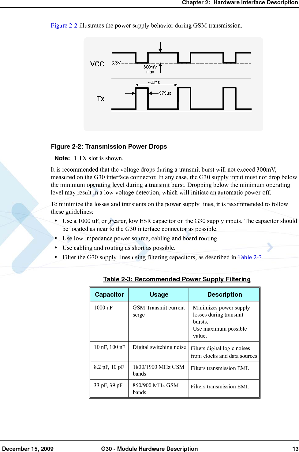
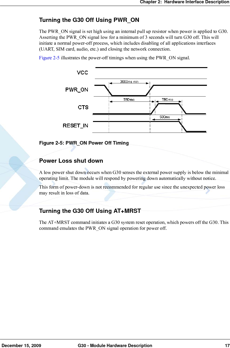
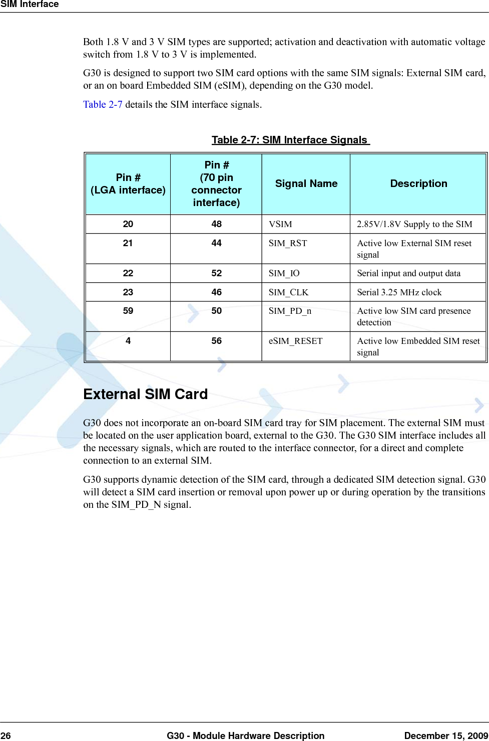
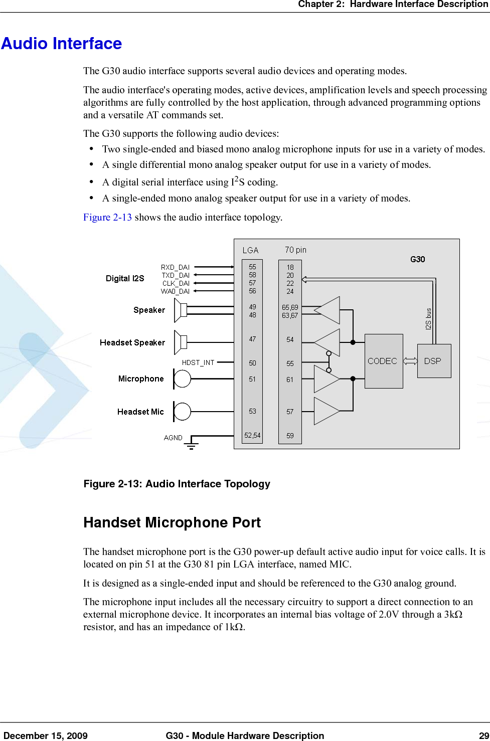
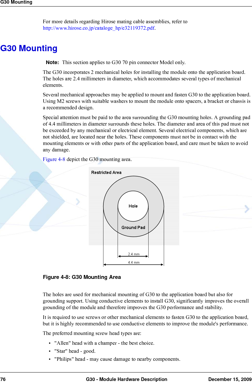
![How to Get Warranty Service?xviii G30 - Module Hardware Description December 15, 2009You must inform Motorola of the lack of conformity to the applicable specifications of any of the Products within a period of two (2) months from the date on which you detect a defect in material, workmanship or lack of conformity and in any event within a term not to exceed the Warranty Term, and must immediately submit the Product for service to Motorola's Authorized Repair or Service Center. Motorola shall not be bound by Product related statements not directly made by Motorola nor any warranty obligations applicable to the seller.A list of the Motorola Call Center numbers is enclosed with this Product.During the Warranty term, Motorola will, at its discretion and without extra charge, as your exclusive remedy, repair or replace your Product which does not comply with this warranty; or failing this, to reimburse the price of the Product but reduced to take into account the use you have had of the Product since it was delivered. This warranty will expire at the end of the Warranty Term.This is the complete and exclusive warranty for a Motorola OEM module and accessories and in lieu of all other warranties, terms and conditions, whether express or implied.Where you purchase the product other than as a consumer, Motorola disclaims all other warranties, terms and conditions express or implied, such as fitness for purpose and satisfactory quality.In no event shall Motorola be liable for damages nor loss of data in excess of the purchase price nor for any incidental special or consequential damages* arising out of the use or inability to use the Product, to the full extent such may be disclaimed by law.This Warranty does not affect any statutory rights that you may have if you are a consumer, such as a warranty of satisfactory quality and fit for the purpose for which products of the same type are normally used under normal use and service, nor any rights against the seller of the Products arising from your purchase and sales contract.(*)including without limitation loss of use, loss of time, loss of data, inconvenience, commercial loss, lost profits or savings.How to Get Warranty Service?In most cases the authorized Motorola dealer which sold and/or installed your Motorola OEM module and original accessories will honor a warranty claim and/or provide warranty service. Alternatively, for further information on how to get warranty service please contact Customer care group (refer to “Service and Testing” ).ClaimingIn order to claim the warranty service you must return the OEM module and/or accessories in question to Motorola's Authorized Repair or Service Center in the original configuration and packaging as supplied by Motorola. Please avoid leaving any supplementary items like SIM cards. The Product should also be accompanied by a label with your name, address, and telephone number; name of operator and a description of the problem.In order to be eligible to receive warranty service, you must present your receipt of purchase or a comparable substitute proof of purchase bearing the date of purchase. The module should also clearly display the original compatible electronic serial number (IMEI) and mechanic serial number [MSN]. Such information is contained with the Product.You must ensure that all and any repairs or servicing is handled at all times by a Motorola Authorized Service Center in accordance with the Motorola Service requirements.](https://usermanual.wiki/Motorola-Mobility/T56KT1/User-Guide-1235883-Page-20.png)