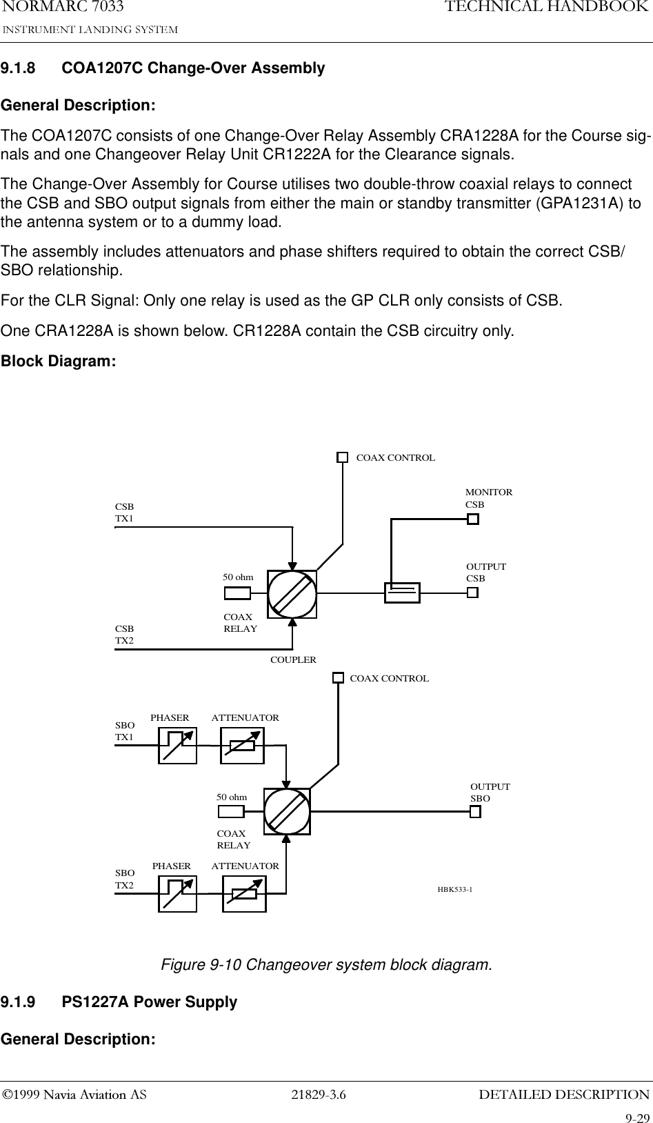
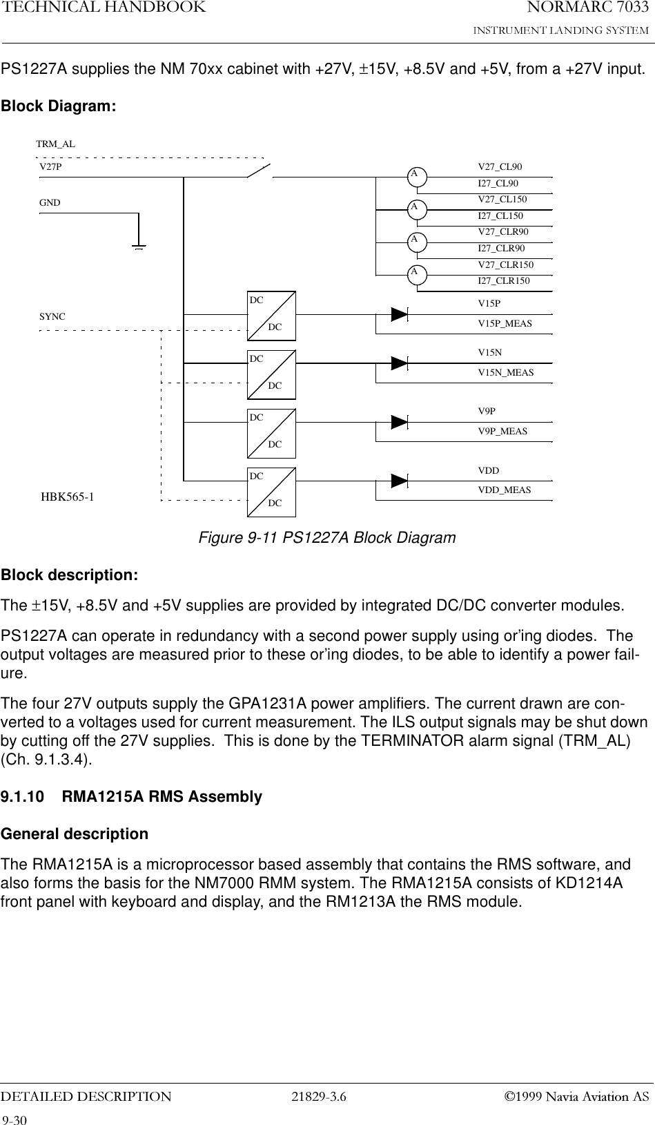
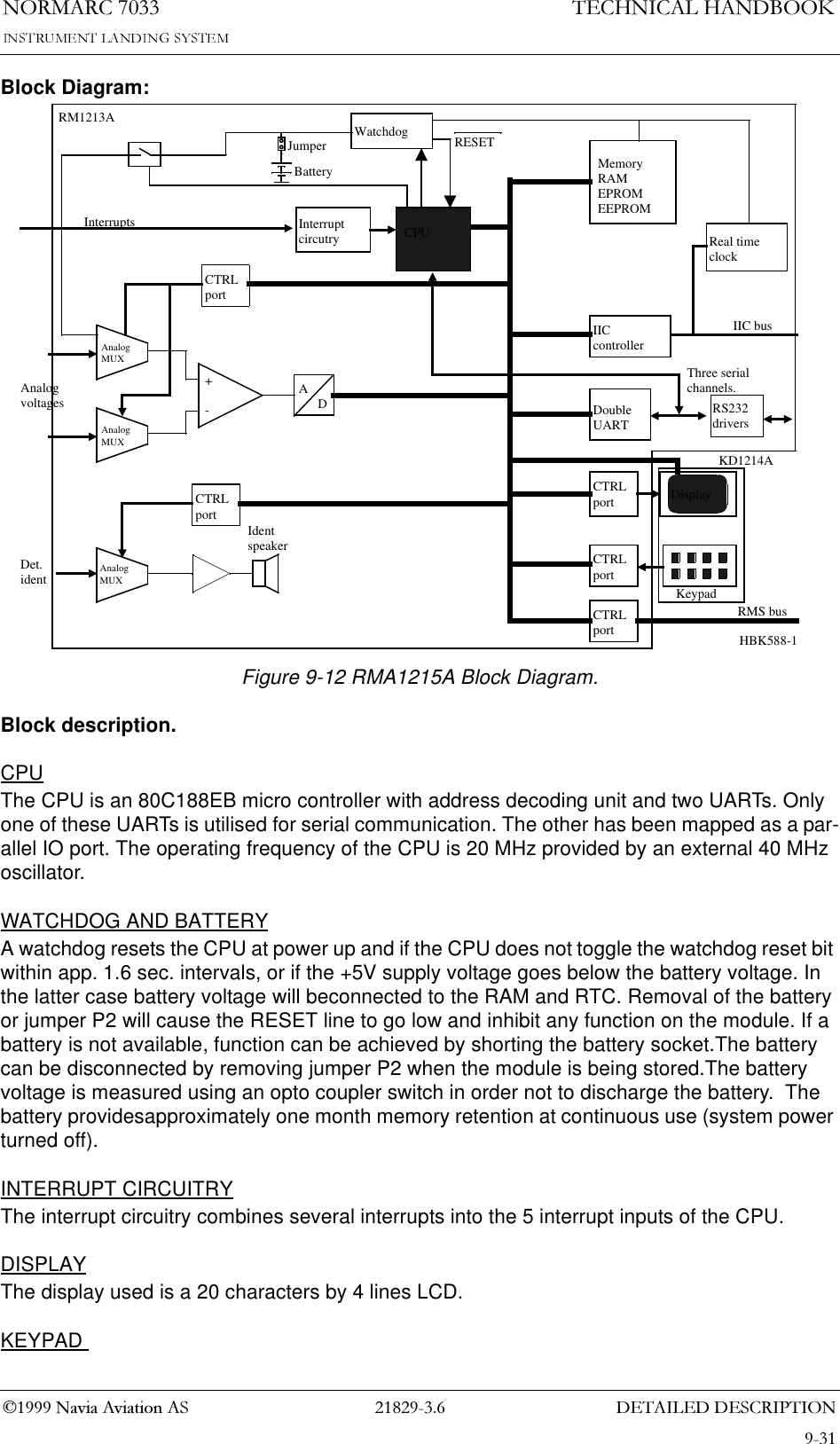
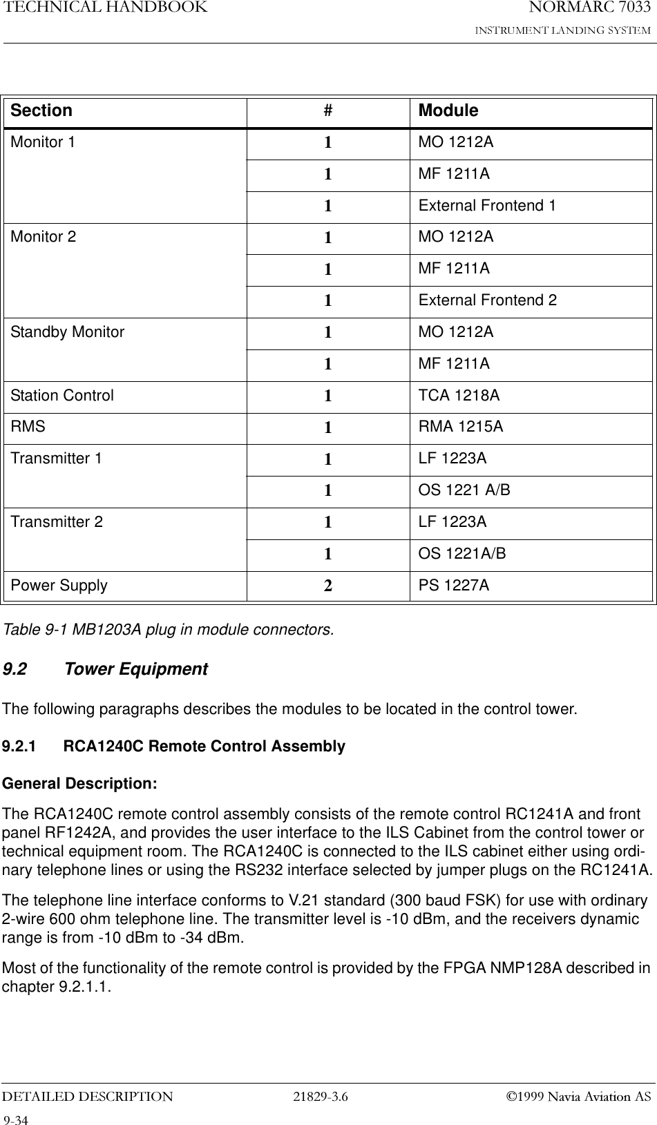
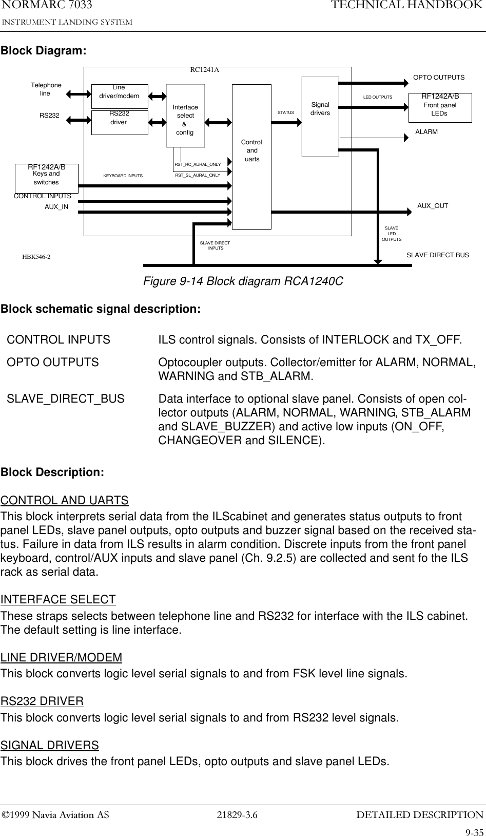
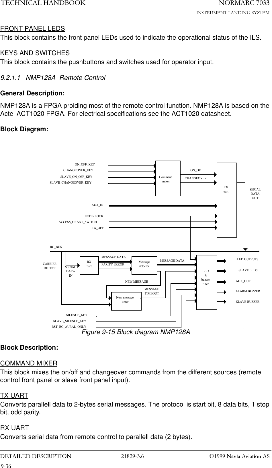
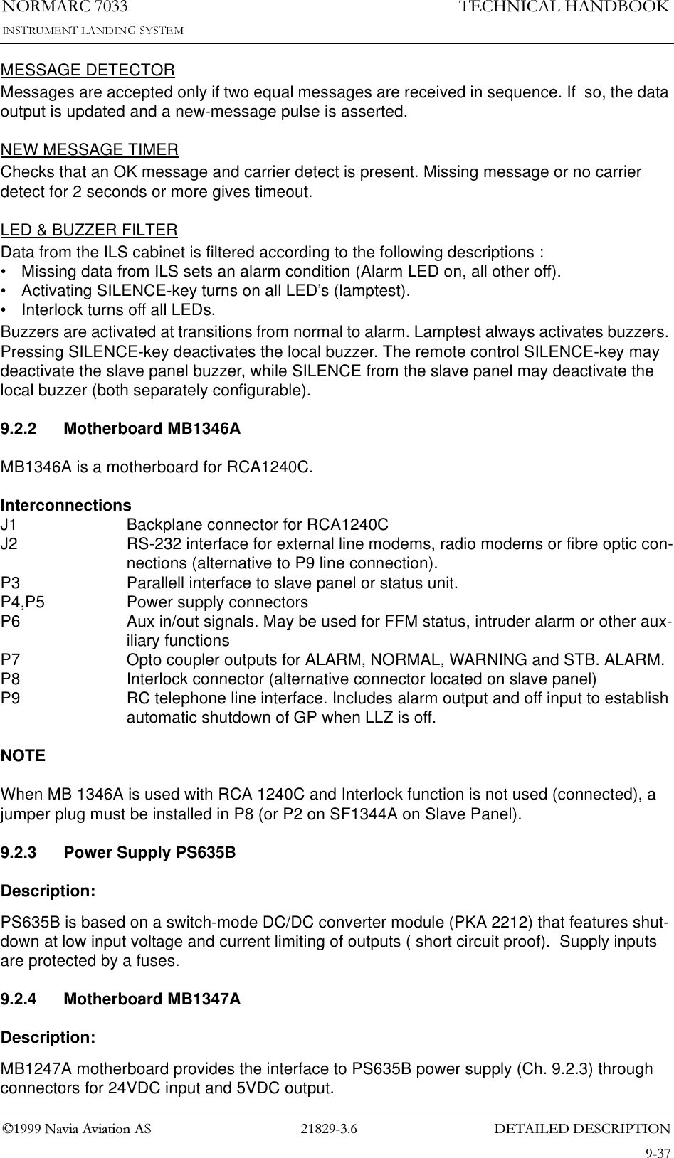
Leidos NORMARC7033 7033 Dual Frequency Glide Path User Manual

Lockheed Martin Air Traffic Management 7033 Dual Frequency Glide Path

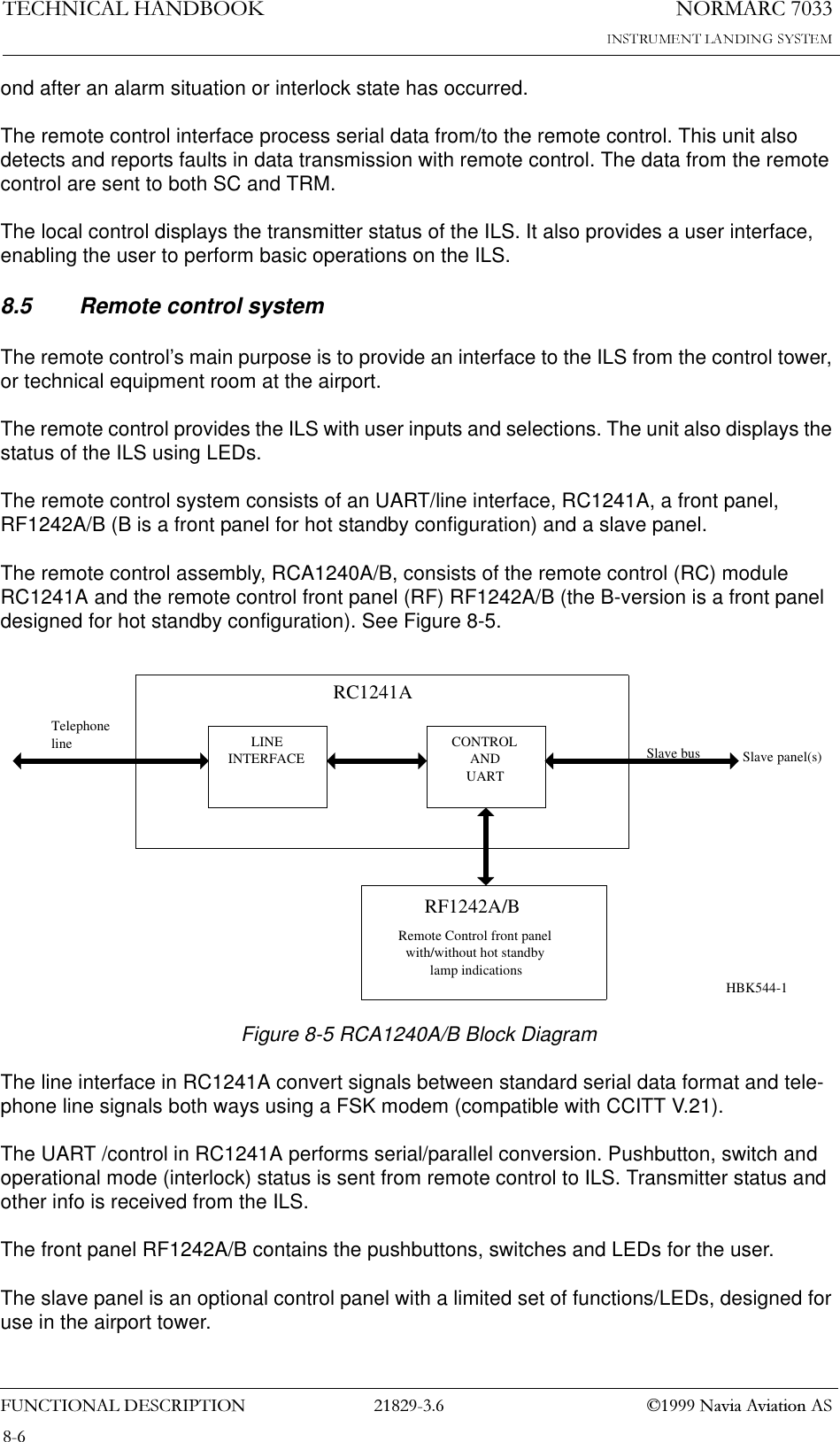
Normarc 7033 ILS Technical Handbook
1250$5&INSTRUMENT LANDING SYSTEMTechnical Handbook21829-3.6©1999 Navia Aviation AS
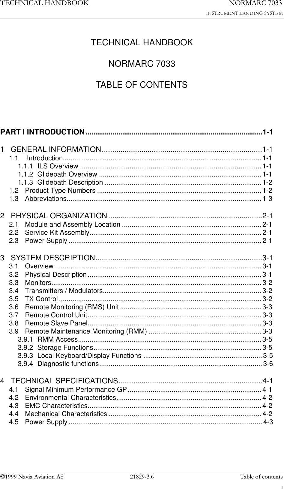
7(&+1,&$/+$1'%22.1DYLD$YLDWLRQ$6 LTECHNICAL HANDBOOKNORMARC 7033TABLE OF CONTENTS1250$5&7DEOHRIFRQWHQWVPART I INTRODUCTION.....................................................................................1-11 GENERAL INFORMATION.............................................................................1-11.1  Introduction........................................................................................................1-11.1.1 ILS Overview ............................................................................................... 1-11.1.2 Glidepath Overview ..................................................................................... 1-11.1.3 Glidepath Description ..................................................................................1-21.2 Product Type Numbers ...................................................................................... 1-21.3 Abbreviations...................................................................................................... 1-32 PHYSICAL ORGANIZATION..........................................................................2-12.1 Module and Assembly Location .........................................................................2-12.2 Service Kit Assembly.......................................................................................... 2-12.3 Power Supply.....................................................................................................2-13 SYSTEM DESCRIPTION................................................................................3-13.1 Overview ............................................................................................................3-13.2 Physical Description........................................................................................... 3-13.3 Monitors.............................................................................................................. 3-23.4 Transmitters / Modulators...................................................................................3-23.5 TX Control .......................................................................................................... 3-23.6 Remote Monitoring (RMS) Unit ..........................................................................3-33.7 Remote Control Unit........................................................................................... 3-33.8 Remote Slave Panel........................................................................................... 3-33.9 Remote Maintenance Monitoring (RMM) ...........................................................3-33.9.1 RMM Access................................................................................................ 3-53.9.2 Storage Functions........................................................................................3-53.9.3 Local Keyboard/Display Functions ..............................................................3-53.9.4 Diagnostic functions..................................................................................... 3-64 TECHNICAL SPECIFICATIONS.....................................................................4-14.1 Signal Minimum Performance GP......................................................................4-14.2 Environmental Characteristics............................................................................ 4-24.3 EMC Characteristics........................................................................................... 4-24.4 Mechanical Characteristics ................................................................................ 4-24.5 Power Supply.....................................................................................................4-3
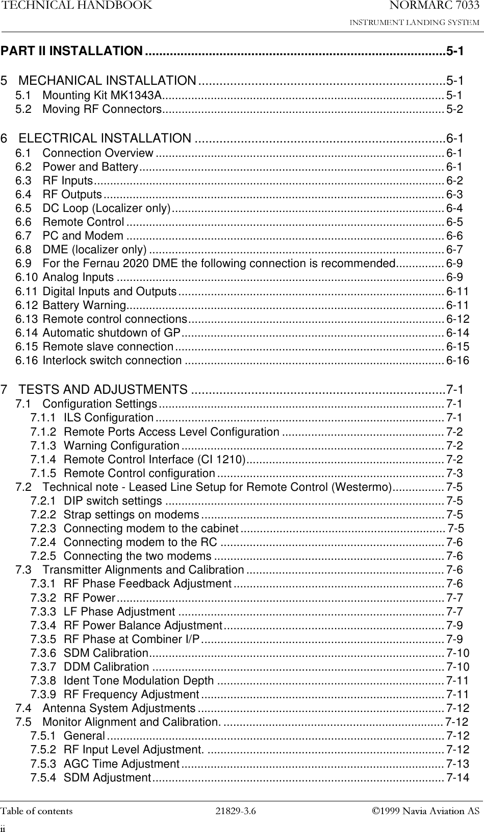
1250$5&7(&+1,&$/+$1'%22.7DEOHRIFRQWHQWV  1DYLD$YLDWLRQ$6LLPART II INSTALLATION .....................................................................................5-15 MECHANICAL INSTALLATION......................................................................5-15.1 Mounting Kit MK1343A.......................................................................................5-15.2 Moving RF Connectors.......................................................................................5-26 ELECTRICAL INSTALLATION .......................................................................6-16.1 Connection Overview .........................................................................................6-16.2 Power and Battery.............................................................................................. 6-16.3 RF Inputs............................................................................................................6-26.4 RF Outputs......................................................................................................... 6-36.5 DC Loop (Localizer only).................................................................................... 6-46.6 Remote Control .................................................................................................. 6-56.7 PC and Modem ..................................................................................................6-66.8 DME (localizer only) ........................................................................................... 6-76.9 For the Fernau 2020 DME the following connection is recommended...............6-96.10 Analog Inputs .....................................................................................................6-96.11 Digital Inputs and Outputs..................................................................................6-116.12 Battery Warning.................................................................................................. 6-116.13 Remote control connections...............................................................................6-126.14 Automatic shutdown of GP................................................................................. 6-146.15 Remote slave connection...................................................................................6-156.16 Interlock switch connection ................................................................................6-167 TESTS AND ADJUSTMENTS ........................................................................7-17.1 Configuration Settings........................................................................................ 7-17.1.1 ILS Configuration ......................................................................................... 7-17.1.2 Remote Ports Access Level Configuration .................................................. 7-27.1.3 Warning Configuration................................................................................. 7-27.1.4 Remote Control Interface (CI 1210).............................................................7-27.1.5 Remote Control configuration...................................................................... 7-37.2 Technical note - Leased Line Setup for Remote Control (Westermo)................7-57.2.1 DIP switch settings ...................................................................................... 7-57.2.2 Strap settings on modems...........................................................................7-57.2.3 Connecting modem to the cabinet...............................................................7-57.2.4 Connecting modem to the RC .....................................................................7-67.2.5 Connecting the two modems .......................................................................7-67.3 Transmitter Alignments and Calibration ............................................................. 7-67.3.1 RF Phase Feedback Adjustment .................................................................7-67.3.2 RF Power..................................................................................................... 7-77.3.3 LF Phase Adjustment .................................................................................. 7-77.3.4 RF Power Balance Adjustment....................................................................7-97.3.5 RF Phase at Combiner I/P........................................................................... 7-97.3.6 SDM Calibration...........................................................................................7-107.3.7 DDM Calibration .......................................................................................... 7-107.3.8 Ident Tone Modulation Depth ......................................................................7-117.3.9 RF Frequency Adjustment...........................................................................7-117.4 Antenna System Adjustments ............................................................................7-127.5 Monitor Alignment and Calibration.....................................................................7-127.5.1 General ........................................................................................................ 7-127.5.2 RF Input Level Adjustment. .........................................................................7-127.5.3 AGC Time Adjustment................................................................................. 7-137.5.4 SDM Adjustment.......................................................................................... 7-14
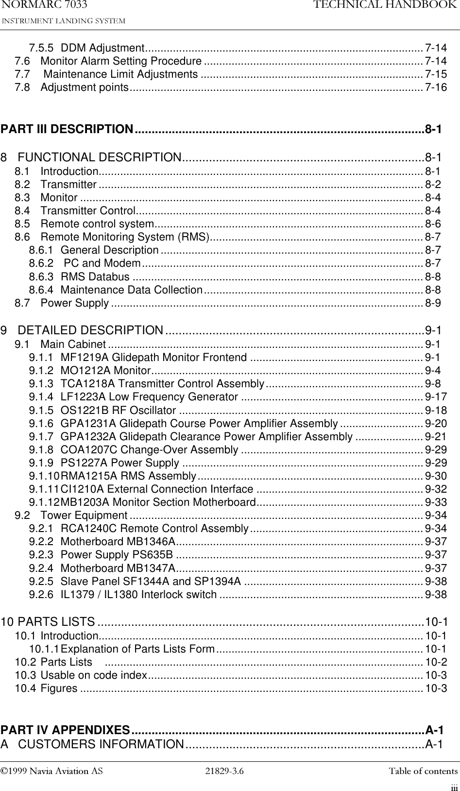
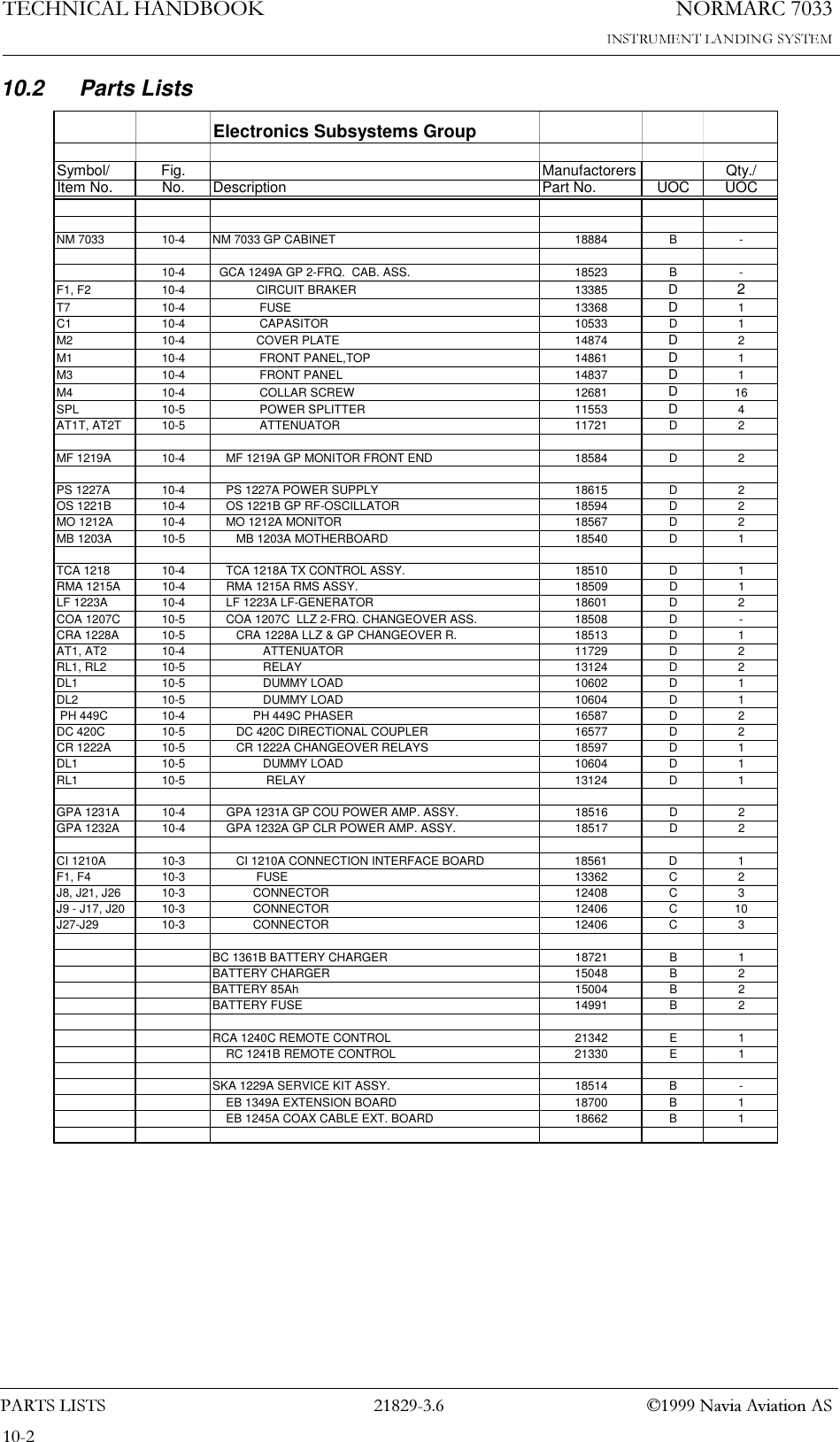
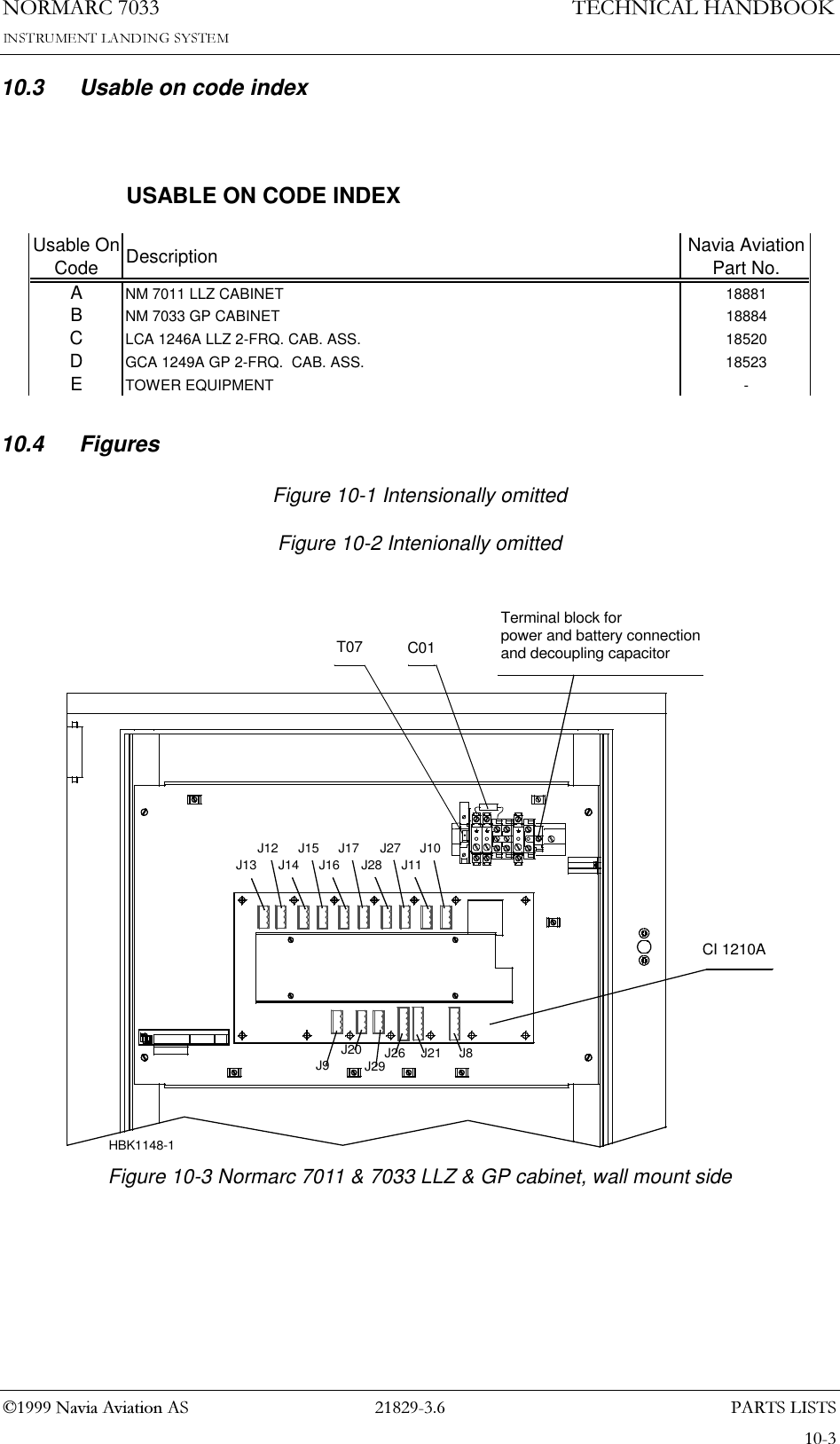
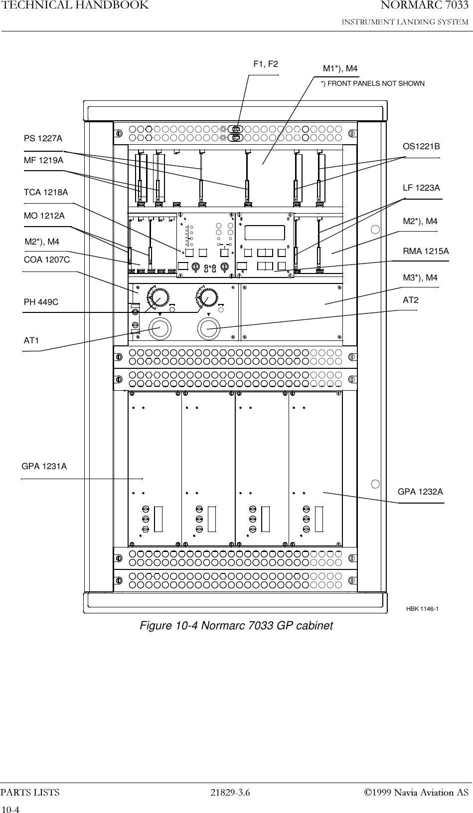
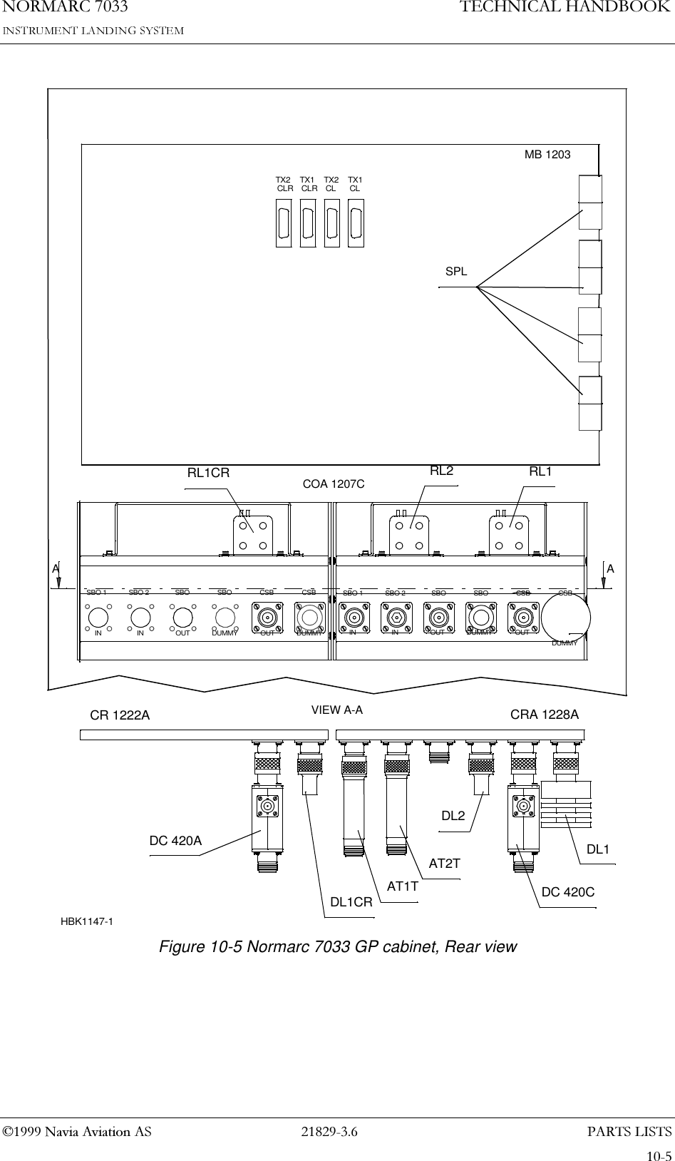
7DEOHRIFRQWHQWV1250$5&LLL1DYLD$YLDWLRQ$67(&+1,&$/+$1'%22.7.5.5 DDM Adjustment.......................................................................................... 7-147.6 Monitor Alarm Setting Procedure .......................................................................7-147.7  Maintenance Limit Adjustments ........................................................................ 7-157.8 Adjustment points............................................................................................... 7-16PART III DESCRIPTION......................................................................................8-18 FUNCTIONAL DESCRIPTION........................................................................8-18.1 Introduction......................................................................................................... 8-18.2 Transmitter ......................................................................................................... 8-28.3 Monitor ............................................................................................................... 8-48.4 Transmitter Control.............................................................................................8-48.5 Remote control system.......................................................................................8-68.6 Remote Monitoring System (RMS).....................................................................8-78.6.1 General Description ..................................................................................... 8-78.6.2  PC and Modem...........................................................................................8-78.6.3 RMS Databus .............................................................................................. 8-88.6.4 Maintenance Data Collection....................................................................... 8-88.7 Power Supply.....................................................................................................8-99 DETAILED DESCRIPTION.............................................................................9-19.1 Main Cabinet ...................................................................................................... 9-19.1.1 MF1219A Glidepath Monitor Frontend ........................................................ 9-19.1.2 MO1212A Monitor........................................................................................9-49.1.3 TCA1218A Transmitter Control Assembly...................................................9-89.1.4 LF1223A Low Frequency Generator ...........................................................9-179.1.5 OS1221B RF Oscillator ............................................................................... 9-189.1.6 GPA1231A Glidepath Course Power Amplifier Assembly...........................9-209.1.7 GPA1232A Glidepath Clearance Power Amplifier Assembly ...................... 9-219.1.8 COA1207C Change-Over Assembly ...........................................................9-299.1.9 PS1227A Power Supply .............................................................................. 9-299.1.10RMA1215A RMS Assembly.........................................................................9-309.1.11CI1210A External Connection Interface ......................................................9-329.1.12MB1203A Monitor Section Motherboard...................................................... 9-339.2 Tower Equipment ............................................................................................... 9-349.2.1 RCA1240C Remote Control Assembly........................................................ 9-349.2.2 Motherboard MB1346A................................................................................9-379.2.3 Power Supply PS635B ................................................................................9-379.2.4 Motherboard MB1347A................................................................................9-379.2.5 Slave Panel SF1344A and SP1394A ..........................................................9-389.2.6 IL1379 / IL1380 Interlock switch ..................................................................9-3810 PARTS LISTS .................................................................................................10-110.1 Introduction......................................................................................................... 10-110.1.1Explanation of Parts Lists Form...................................................................10-110.2 Parts Lists    ....................................................................................................... 10-210.3 Usable on code index......................................................................................... 10-310.4 Figures ............................................................................................................... 10-3PART IV APPENDIXES.......................................................................................A-1A  CUSTOMERS INFORMATION.......................................................................A-1
1250$5&7(&+1,&$/+$1'%22.7DEOHRIFRQWHQWV  1DYLD$YLDWLRQ$6LY
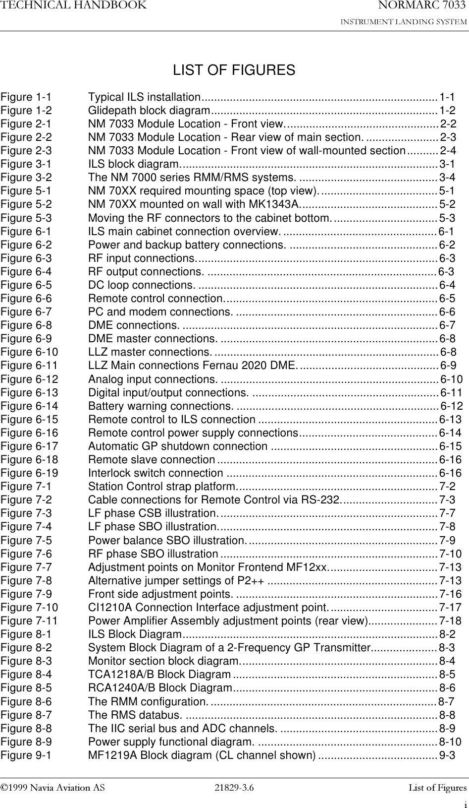
7(&+1,&$/+$1'%22.1DYLD$YLDWLRQ$6 LLIST OF FIGURES1250$5&/LVWRI)LJXUHVFigure 1-1 Typical ILS installation...........................................................................1-1Figure 1-2 Glidepath block diagram........................................................................1-2Figure 2-1 NM 7033 Module Location - Front view.................................................2-2Figure 2-2 NM 7033 Module Location - Rear view of main section. .......................2-3Figure 2-3 NM 7033 Module Location - Front view of wall-mounted section..........2-4Figure 3-1 ILS block diagram..................................................................................3-1Figure 3-2 The NM 7000 series RMM/RMS systems. ............................................3-4Figure 5-1 NM 70XX required mounting space (top view)......................................5-1Figure 5-2 NM 70XX mounted on wall with MK1343A............................................5-2Figure 5-3 Moving the RF connectors to the cabinet bottom..................................5-3Figure 6-1 ILS main cabinet connection overview..................................................6-1Figure 6-2 Power and backup battery connections. ...............................................6-2Figure 6-3 RF input connections.............................................................................6-3Figure 6-4 RF output connections. .........................................................................6-3Figure 6-5 DC loop connections. ............................................................................6-4Figure 6-6 Remote control connection....................................................................6-5Figure 6-7 PC and modem connections. ................................................................6-6Figure 6-8 DME connections. .................................................................................6-7Figure 6-9 DME master connections. .....................................................................6-8Figure 6-10 LLZ master connections. .......................................................................6-8Figure 6-11 LLZ Main connections Fernau 2020 DME.............................................6-9Figure 6-12 Analog input connections. .....................................................................6-10Figure 6-13 Digital input/output connections. ...........................................................6-11Figure 6-14 Battery warning connections. ................................................................6-12Figure 6-15 Remote control to ILS connection .........................................................6-13Figure 6-16 Remote control power supply connections............................................6-14Figure 6-17 Automatic GP shutdown connection .....................................................6-15Figure 6-18 Remote slave connection ......................................................................6-16Figure 6-19 Interlock switch connection ...................................................................6-16Figure 7-1 Station Control strap platform................................................................7-2Figure 7-2 Cable connections for Remote Control via RS-232...............................7-3Figure 7-3 LF phase CSB illustration......................................................................7-7Figure 7-4 LF phase SBO illustration......................................................................7-8Figure 7-5 Power balance SBO illustration.............................................................7-9Figure 7-6 RF phase SBO illustration .....................................................................7-10Figure 7-7 Adjustment points on Monitor Frontend MF12xx...................................7-13Figure 7-8 Alternative jumper settings of P2++ ......................................................7-13Figure 7-9 Front side adjustment points. ................................................................7-16Figure 7-10 CI1210A Connection Interface adjustment point...................................7-17Figure 7-11 Power Amplifier Assembly adjustment points (rear view)......................7-18Figure 8-1 ILS Block Diagram.................................................................................8-2Figure 8-2 System Block Diagram of a 2-Frequency GP Transmitter.....................8-3Figure 8-3 Monitor section block diagram...............................................................8-4Figure 8-4 TCA1218A/B Block Diagram.................................................................8-5Figure 8-5 RCA1240A/B Block Diagram.................................................................8-6Figure 8-6 The RMM configuration.........................................................................8-7Figure 8-7 The RMS databus. ................................................................................8-8Figure 8-8 The IIC serial bus and ADC channels. ..................................................8-9Figure 8-9 Power supply functional diagram. .........................................................8-10Figure 9-1 MF1219A Block diagram (CL channel shown) ......................................9-3
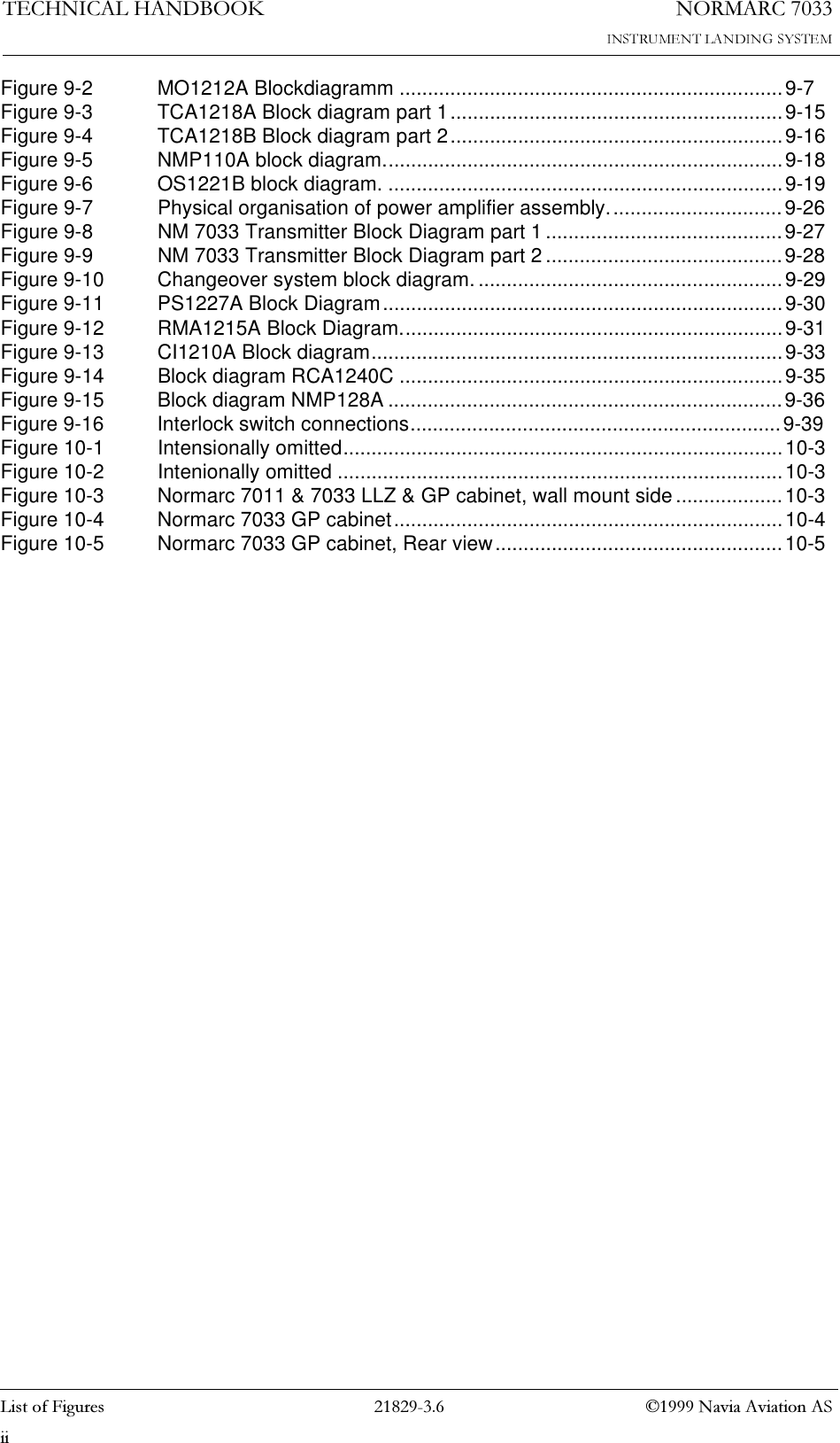
1250$5&7(&+1,&$/+$1'%22./LVWRI)LJXUHV  1DYLD$YLDWLRQ$6LLFigure 9-2 MO1212A Blockdiagramm ....................................................................9-7Figure 9-3 TCA1218A Block diagram part 1...........................................................9-15Figure 9-4 TCA1218B Block diagram part 2...........................................................9-16Figure 9-5 NMP110A block diagram.......................................................................9-18Figure 9-6 OS1221B block diagram. ......................................................................9-19Figure 9-7 Physical organisation of power amplifier assembly...............................9-26Figure 9-8 NM 7033 Transmitter Block Diagram part 1 ..........................................9-27Figure 9-9 NM 7033 Transmitter Block Diagram part 2 ..........................................9-28Figure 9-10 Changeover system block diagram. ......................................................9-29Figure 9-11 PS1227A Block Diagram.......................................................................9-30Figure 9-12 RMA1215A Block Diagram....................................................................9-31Figure 9-13 CI1210A Block diagram.........................................................................9-33Figure 9-14 Block diagram RCA1240C ....................................................................9-35Figure 9-15 Block diagram NMP128A ......................................................................9-36Figure 9-16 Interlock switch connections..................................................................9-39Figure 10-1 Intensionally omitted..............................................................................10-3Figure 10-2 Intenionally omitted ...............................................................................10-3Figure 10-3 Normarc 7011 & 7033 LLZ & GP cabinet, wall mount side...................10-3Figure 10-4 Normarc 7033 GP cabinet.....................................................................10-4Figure 10-5 Normarc 7033 GP cabinet, Rear view...................................................10-5
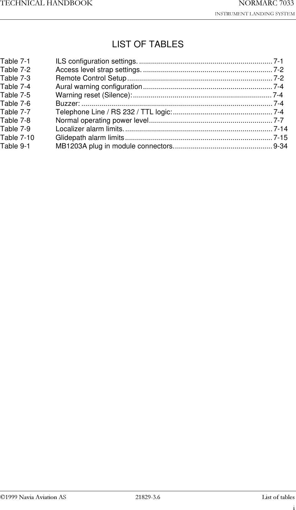
7(&+1,&$/+$1'%22.1DYLD$YLDWLRQ$6 LLIST OF TABLES1250$5&/LVWRIWDEOHVTable 7-1 ILS configuration settings. ...................................................................7-1Table 7-2 Access level strap settings..................................................................7-2Table 7-3 Remote Control Setup.........................................................................7-2Table 7-4 Aural warning configuration.................................................................7-4Table 7-5 Warning reset (Silence):......................................................................7-4Table 7-6 Buzzer: ................................................................................................7-4Table 7-7 Telephone Line / RS 232 / TTL logic:.................................................. 7-4Table 7-8 Normal operating power level..............................................................7-7Table 7-9 Localizer alarm limits...........................................................................7-14Table 7-10 Glidepath alarm limits..........................................................................7-15Table 9-1 MB1203A plug in module connectors..................................................9-34
1250$5&7(&+1,&$/+$1'%22./LVWRIWDEOHV  1DYLD$YLDWLRQ$6LL
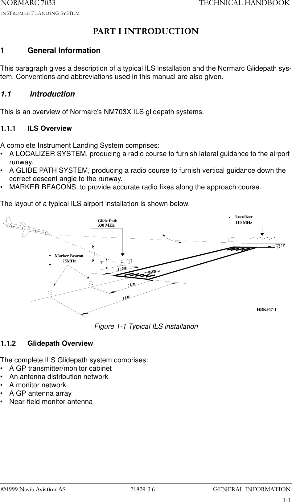
*(1(5$/,1)250$7,211250$5&1DYLD$YLDWLRQ$67(&+1,&$/+$1'%22.3$57,,1752'8&7,211 General InformationThis paragraph gives a description of a typical ILS installation and the Normarc Glidepath sys-tem. Conventions and abbreviations used in this manual are also given.1.1  IntroductionThis is an overview of Normarc’s NM703X ILS glidepath systems.1.1.1 ILS OverviewA complete Instrument Landing System comprises:• A LOCALIZER SYSTEM, producing a radio course to furnish lateral guidance to the airport runway.• A GLIDE PATH SYSTEM, producing a radio course to furnish vertical guidance down the correct descent angle to the runway.• MARKER BEACONS, to provide accurate radio fixes along the approach course.The layout of a typical ILS airport installation is shown below.Figure 1-1 Typical ILS installation1.1.2 Glidepath OverviewThe complete ILS Glidepath system comprises:• A GP transmitter/monitor cabinet• An antenna distribution network• A monitor network• A GP antenna array• Near-field monitor antennaLocalizer110 MHzGlide Path330 MHzMarker Beacon75MHz3°HBK547-1
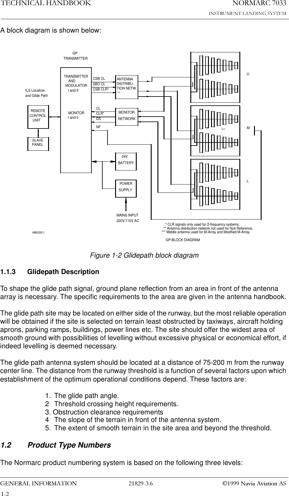
1250$5&7(&+1,&$/+$1'%22.*(1(5$/,1)250$7,21  1DYLD$YLDWLRQ$6A block diagram is shown below: Figure 1-2 Glidepath block diagram1.1.3 Glidepath DescriptionTo shape the glide path signal, ground plane reflection from an area in front of the antenna array is necessary. The specific requirements to the area are given in the antenna handbook.The glide path site may be located on either side of the runway, but the most reliable operation will be obtained if the site is selected on terrain least obstructed by taxiways, aircraft holding aprons, parking ramps, buildings, power lines etc. The site should offer the widest area of smooth ground with possibilities of levelling without excessive physical or economical effort, if indeed levelling is deemed necessary.The glide path antenna system should be located at a distance of 75-200 m from the runway center line. The distance from the runway threshold is a function of several factors upon which establishment of the optimum operational conditions depend. These factors are:1. The glide path angle.2 Threshold crossing height requirements.3. Obstruction clearance requirements 4 The slope of the terrain in front of the antenna system.5. The extent of smooth terrain in the site area and beyond the threshold.1.2 Product Type NumbersThe Normarc product numbering system is based on the following three levels:GP-BLOCK DIAGRAMHBK205-1TRANSMITTER   ANDMODULATOR I and IIMONITOR I and IIREMOTECONTROLUNITSLAVEPANELCSB CLSBO CLCSB CLR*CLCLR*DSNFANTENNADISTRIBU-TION NETW.**MONITORNETWORK24VBATTERYSUPPLYPOWERMAINS INPUT220V/110V ACULMILS Localizerand Glide PathGPTRANSMITTER**** CLR signals only used for 2-frequency systems.** Antenna distribution network not used for Null Reference.*** Middle antenna used for M-Array and Modified M-Array.
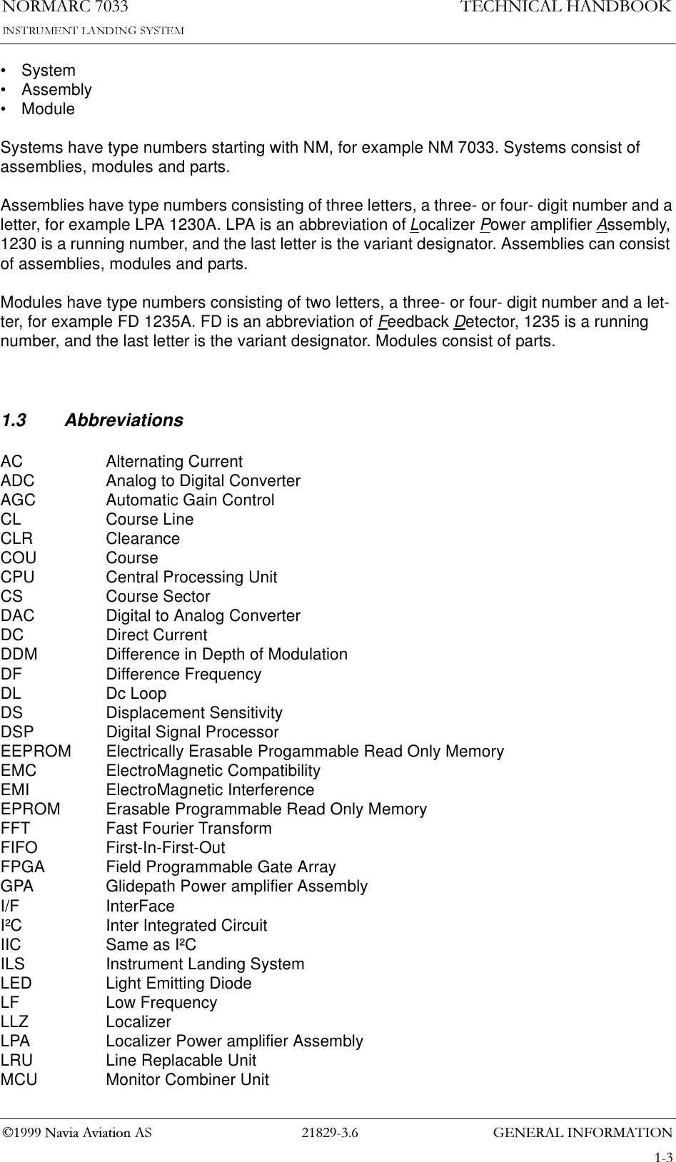
*(1(5$/,1)250$7,211250$5&1DYLD$YLDWLRQ$67(&+1,&$/+$1'%22.•System• Assembly• ModuleSystems have type numbers starting with NM, for example NM 7033. Systems consist of assemblies, modules and parts.Assemblies have type numbers consisting of three letters, a three- or four- digit number and a letter, for example LPA 1230A. LPA is an abbreviation of Localizer Power amplifier Assembly, 1230 is a running number, and the last letter is the variant designator. Assemblies can consist of assemblies, modules and parts.Modules have type numbers consisting of two letters, a three- or four- digit number and a let-ter, for example FD 1235A. FD is an abbreviation of Feedback Detector, 1235 is a running number, and the last letter is the variant designator. Modules consist of parts.1.3 AbbreviationsAC Alternating CurrentADC Analog to Digital ConverterAGC Automatic Gain ControlCL Course LineCLR ClearanceCOU CourseCPU Central Processing UnitCS Course SectorDAC Digital to Analog ConverterDC Direct CurrentDDM Difference in Depth of ModulationDF Difference FrequencyDL Dc LoopDS Displacement SensitivityDSP Digital Signal ProcessorEEPROM Electrically Erasable Progammable Read Only MemoryEMC ElectroMagnetic CompatibilityEMI ElectroMagnetic InterferenceEPROM Erasable Programmable Read Only MemoryFFT Fast Fourier TransformFIFO First-In-First-OutFPGA Field Programmable Gate ArrayGPA Glidepath Power amplifier AssemblyI/F InterFaceI²C Inter Integrated CircuitIIC Same as I²CILS Instrument Landing SystemLED Light Emitting DiodeLF Low FrequencyLLZ LocalizerLPA Localizer Power amplifier AssemblyLRU Line Replacable UnitMCU Monitor Combiner Unit
1250$5&7(&+1,&$/+$1'%22.*(1(5$/,1)250$7,21  1DYLD$YLDWLRQ$6NAV NAVigation signalsNF Near FieldPC Personal ComputerRAM Random Access MemoryRF Radio FrequencyRMM Remote Maintenance MonitorRMS Remote Monitoring SystemROM Read Only MemoryRTC Real Time ClockSC Station ControlSDM Sum in Depth of ModulationSPA Same Parameter AlarmSRAM Static Random Access MemorySTB StandbySW SoftWareTRM TeRMinatorTX Transmitter
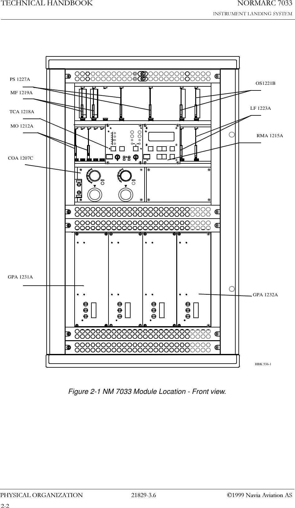
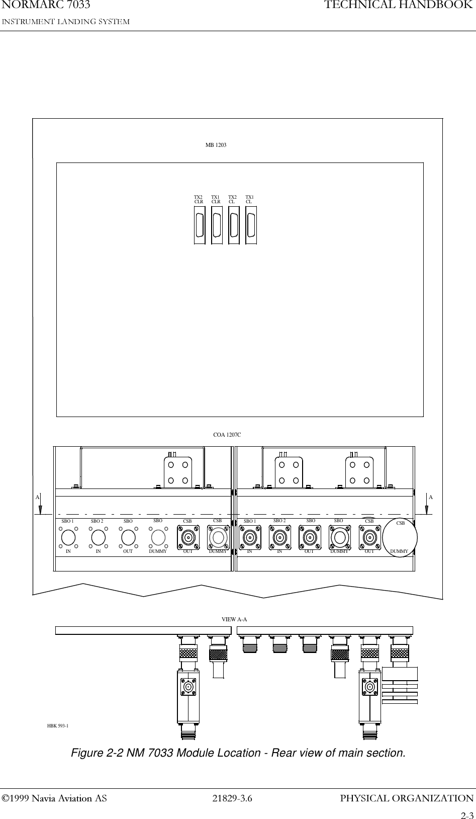
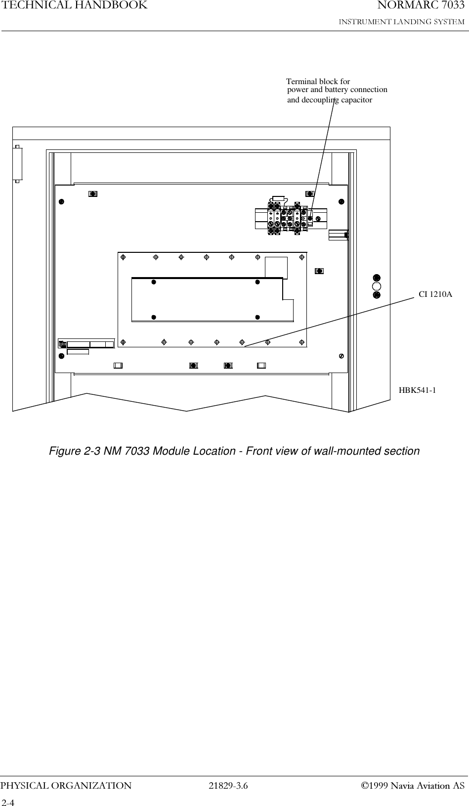
3+<6,&$/25*$1,=$7,211250$5&1DYLD$YLDWLRQ$67(&+1,&$/+$1'%22.2 Physical Organization2.1 Module and Assembly LocationThe figures on the following pages show the locations of the modules in the main cabinet.Figure 2-1 shows the main section of the GP cabinet from a front view, with indications of the plug-in board locations.Figure 2-2 shows the same section from a rear view, while Figure 2-3 shows the top half of the wall-mounted section.In addition, the Remote Control Assembly RCA1240C/D and Remote Slave SF 1344A are installed in the technical control room and the control tower, respectively.2.2 Service Kit AssemblyThe Service Kit Assembly SKA 1229A includes two different extension boards for mainte-nance operations:EB1349A Extension Board - for use with the Power Supply PS1227A, Monitor MO1212A, RMS Assembly RMA1215A, Transmitter Control Assembly TCA1218A/B and Low Frequency Generator LF1223A plug-in boards.EB1245A Extension Board with coax cables - for use with Monitor Frontend MF1219A and Oscillator OS1221B plug-in boards.In addition, the following items are included:• Static-dissipative work mat and wrist strap to ensure ESD-protected environment when performing maintenance operations on the equipment.• Torque wrench, screw drivers etc.2.3 Power SupplyAn External Power Supply, operating at 230V/120V mains input and providing 27V at 20A, is normally supplied with the equipment. In special cases, a second external power supply is supplied.
1250$5&7(&+1,&$/+$1'%22.3+<6,&$/25*$1,=$7,21  1DYLD$YLDWLRQ$6         Figure 2-1 NM 7033 Module Location - Front view.11LF 1223AOS1221BCOA 1207CMO 1212AMF 1219APS 1227AGPA 1231ARMA 1215ATCA 1218AGPA 1232AHBK 536-1
3+<6,&$/25*$1,=$7,211250$5&1DYLD$YLDWLRQ$67(&+1,&$/+$1'%22. Figure 2-2 NM 7033 Module Location - Rear view of main section.SBO 1IN IN OUTSBO 2 SBODUMMY OUTSBO CSBDUMMY INCSB SBO 1IN OUTSBO 2 SBODUMMY OUTSBO CSBDUMMYCSBMB 1203COA 1207CTX1CLTX2CLTX1CLRTX2CLRAAVIEW A-AHBK 593-1
1250$5&7(&+1,&$/+$1'%22.3+<6,&$/25*$1,=$7,21  1DYLD$YLDWLRQ$6Figure 2-3 NM 7033 Module Location - Front view of wall-mounted sectionCI 1210ATerminal block forpower and battery connectionand decoupling capacitorHBK541-1
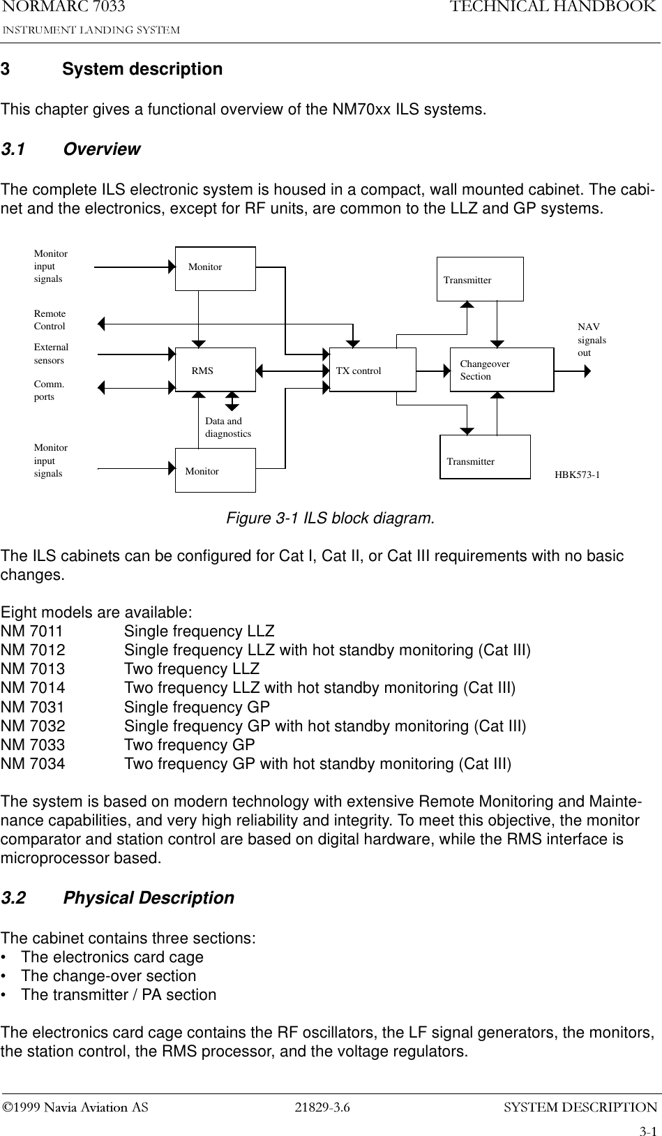
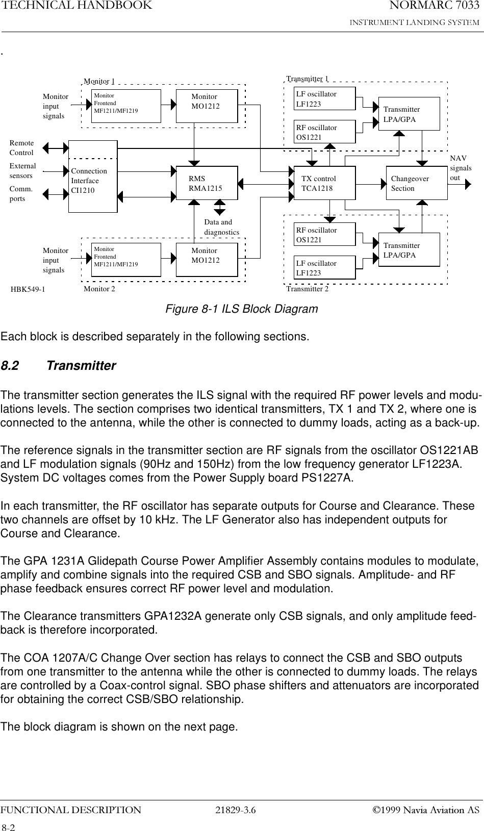
6<67(0'(6&5,37,211250$5&1DYLD$YLDWLRQ$67(&+1,&$/+$1'%22.3 System descriptionThis chapter gives a functional overview of the NM70xx ILS systems.3.1 OverviewThe complete ILS electronic system is housed in a compact, wall mounted cabinet. The cabi-net and the electronics, except for RF units, are common to the LLZ and GP systems.Figure 3-1 ILS block diagram.The ILS cabinets can be configured for Cat I, Cat II, or Cat III requirements with no basic changes.Eight models are available:NM 7011 Single frequency LLZNM 7012 Single frequency LLZ with hot standby monitoring (Cat III)NM 7013 Two frequency LLZNM 7014 Two frequency LLZ with hot standby monitoring (Cat III)NM 7031 Single frequency GPNM 7032 Single frequency GP with hot standby monitoring (Cat III)NM 7033 Two frequency GPNM 7034 Two frequency GP with hot standby monitoring (Cat III)The system is based on modern technology with extensive Remote Monitoring and Mainte-nance capabilities, and very high reliability and integrity. To meet this objective, the monitor comparator and station control are based on digital hardware, while the RMS interface is microprocessor based.3.2 Physical DescriptionThe cabinet contains three sections:• The electronics card cage• The change-over section• The transmitter / PA sectionThe electronics card cage contains the RF oscillators, the LF signal generators, the monitors, the station control, the RMS processor, and the voltage regulators.MonitorRMSMonitorTX control ChangeoverSectionMonitorinputsignalsMonitorinputsignals TransmitterTransmitterNAVsignalsoutRemoteControlExternalsensorsComm.portsData anddiagnosticsHBK573-1
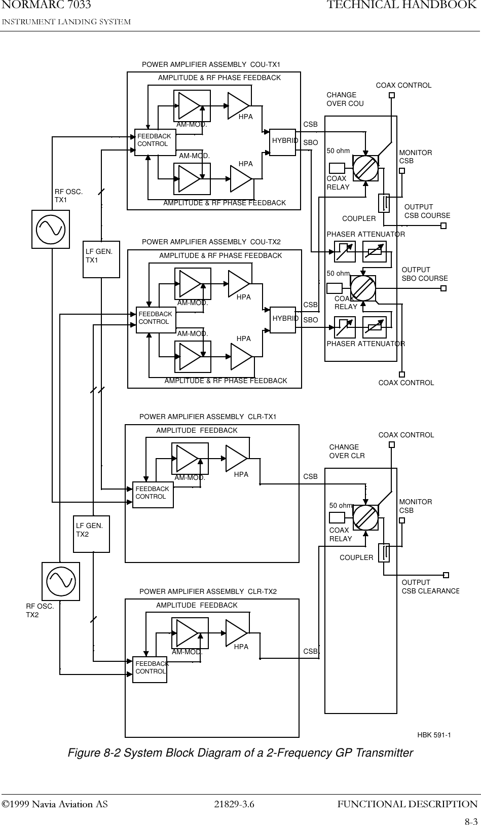
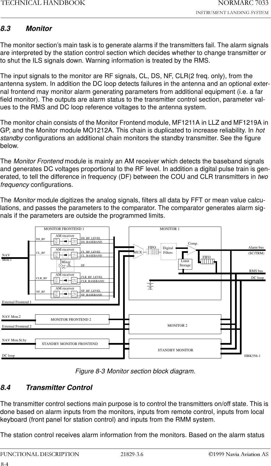
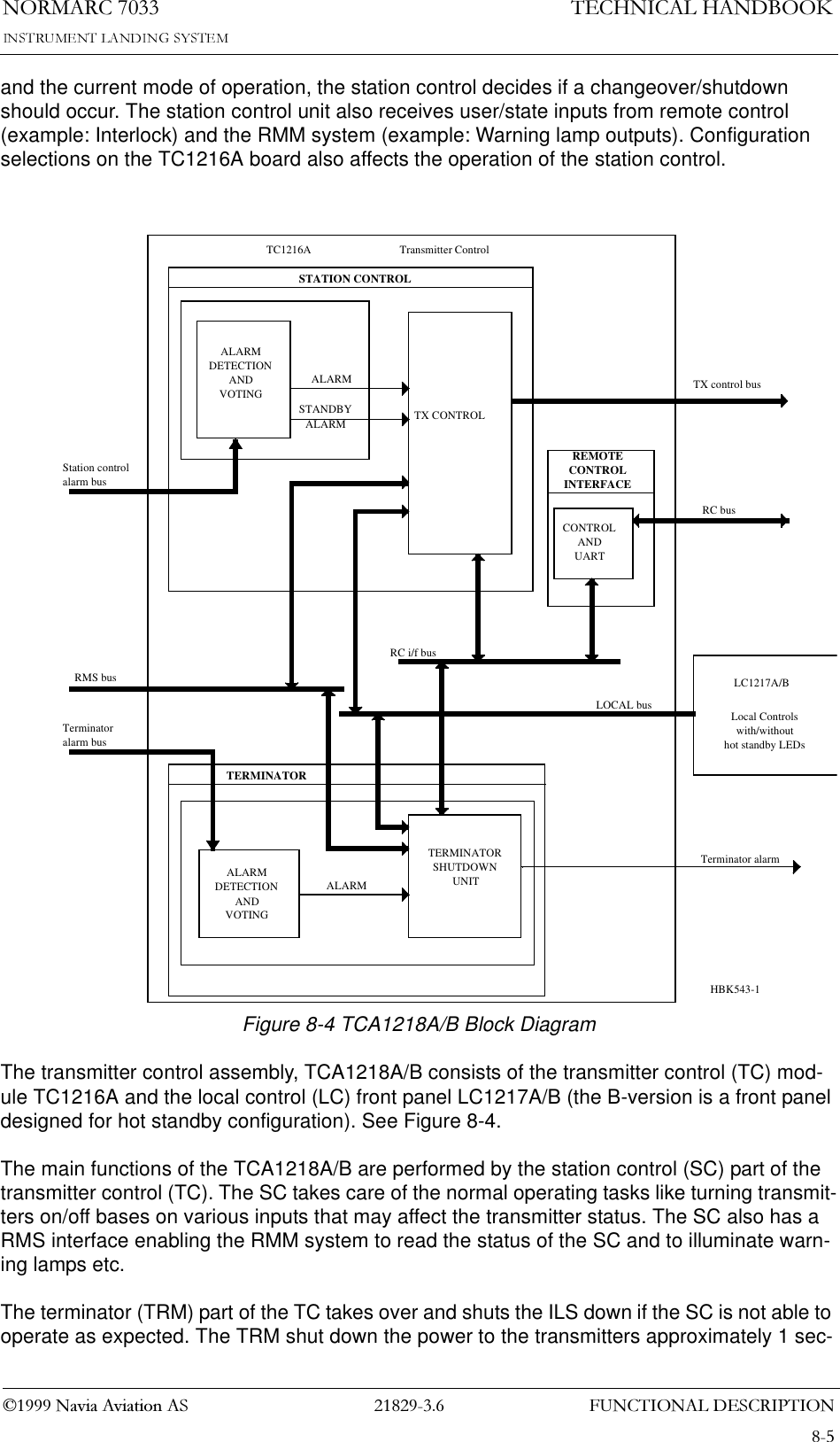
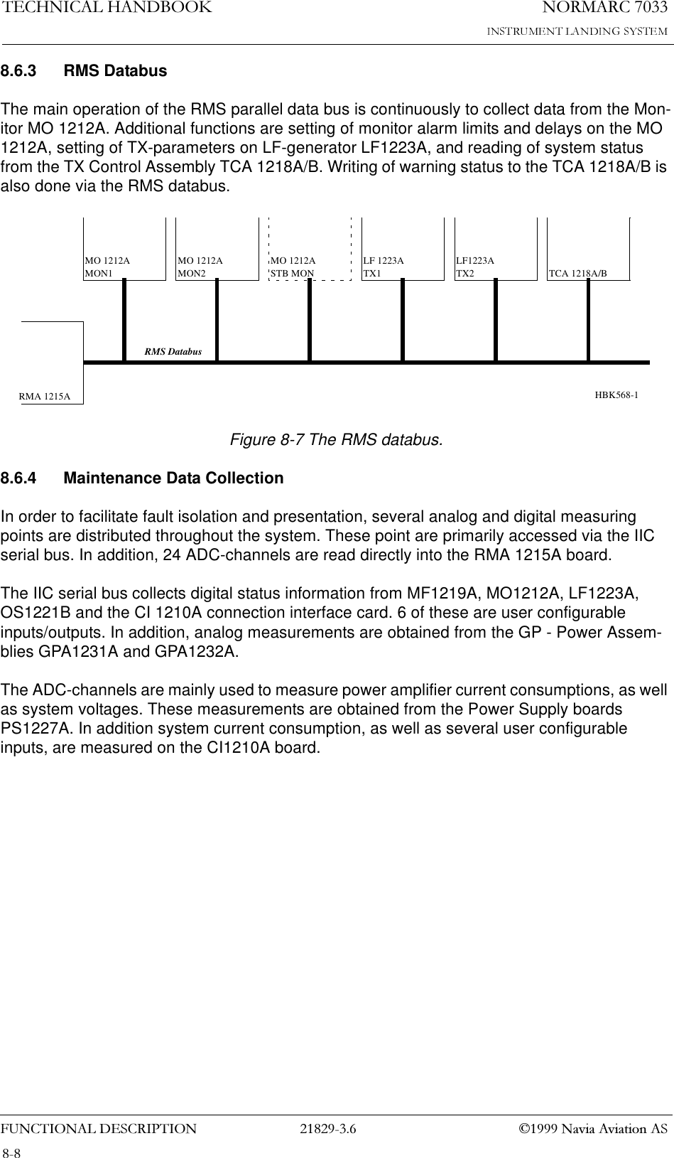
1250$5&7(&+1,&$/+$1'%22.6<67(0'(6&5,37,21  1DYLD$YLDWLRQ$6The change-over section contains coaxial relays, attenuators and phasers for the RF outputs.The transmitter / PA section contains the PA blocks including couplers etc. for each output.The cabinet is divided in two parts, with the rear part fixed to a wall, and the front part hinged to give access to interior of the cabinet.All external connections are made to the rear part of the cabinet.3.3 MonitorsThe ILS has duplicated monitors with inputs for Course Line (CL), Displacement Sensitivity (DS), Near Field (NF), and Clearance (CLR) (Dual Freq. only). The signals are detected by the input stage, and then digitized. In the next block they are filtered by a Fast Fourier Trans-form performed by a signal processor. The results for each parameter is then compared with stored limits in a digital hardware comparator.Each of the two monitors consists of two modules. For Cat III use, Hot Standby monitoring can be added by using one additional monitor and associated RF couplers and combiners.The design of the monitors ensures a very high integrity due to the use of digital hardware for the alarm comparators and a very simple Fast Fourier filtering with a signal processor. In addi-tion, the monitor is checked by automatic self-tests.The alarm limits are stored locally in EEPROM, and can be updated from the RMS processor, with a separate hardware write protection to ensure that the integrity is not affected by the RMS system.3.4 Transmitters / ModulatorsThe transmitters are duplicated, either single frequency or dual frequency. Each transmitter consists of a RF oscillator, a LF generator, and one or two PA blocks (single or dual fre-quency).The RF oscillator uses a synthesizer for easy frequency changes and simple logistics. The oscillator has two outputs for use in dual frequency systems.The LF generator contains the generators for 90Hz, 150Hz and 1020Hz signals, the ident keyer / sequencer and interface for DME master or slave keying. All signals are generated by division from a common clock oscillator, ensuring very stable phase relations between the modulation signals.The modulation balance, modulation sum, RF level and Ident morse code are set in this mod-ule by means of multiplying digital to analog converters. The values are stored locally in EPROM and can be updated from the RMS processor with hardware write protection.The same LF generator is used for single and dual frequency systems.3.5 TX ControlThe TX control unit controls the system dependent on alarms from the monitors and inputs from the local control, the remote control and, optionally, the RMS system. It also generate status information to the same units. The local control and status indicators are a part of the
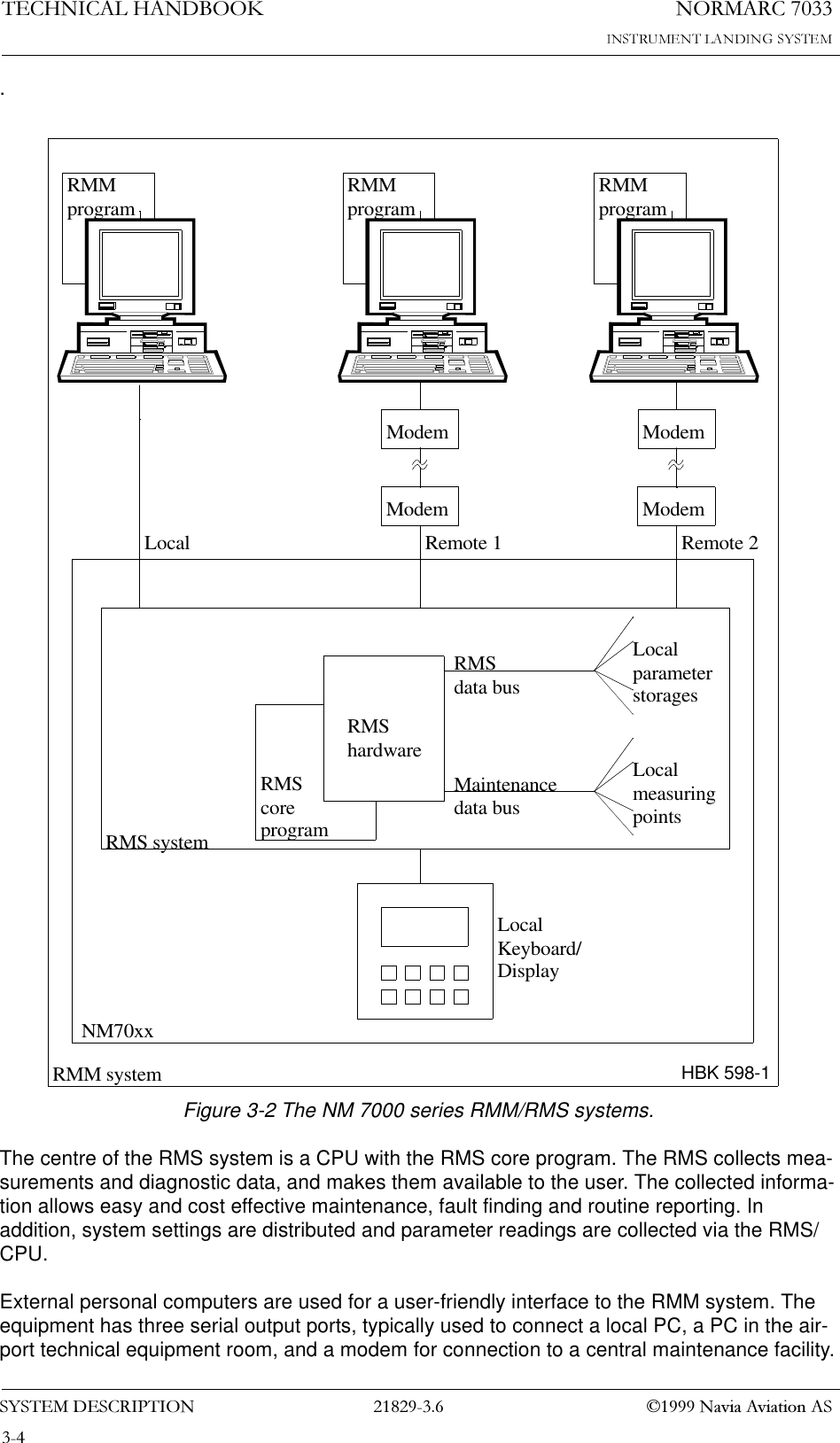
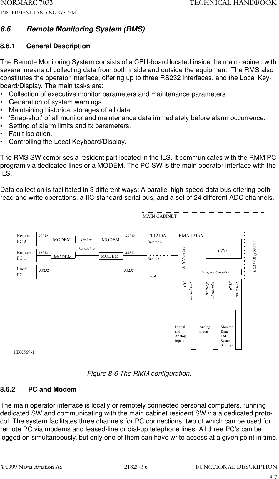
6<67(0'(6&5,37,211250$5&1DYLD$YLDWLRQ$67(&+1,&$/+$1'%22.TX Control unit.All functions in the TX Control are based on digital hardware to ensure the highest integrity.3.6 Remote Monitoring (RMS) UnitThe RMS unit contains the system microprocessor. It handles storage and read-out of monitor parameters, measurements for maintenance and fault finding, and performs fault analysis to isolate faults to line replaceable modules. It is also used to set monitor limits and transmitter adjustments.The RMM handles communication to local and remote RMS computers, and in addition it han-dles a small display and keyboard for parameter setting and readout.3.7 Remote Control UnitThe remote control unit is used in the tower or in the technical control room. It has indicators for operating status as well as detailed warnings and an aural alarm device with reset. It can control equipment on/off and change-over, and has an Access Grant-switch to allow remote control from the RMS system.The Remote Control Unit is connected to the ILS by one telephone pair cable.3.8 Remote Slave PanelThe slave panel is connected to the remote control by a multipair wire. It is intended for use in the control tower. It has indicators for normal / warning / alarm and has an aural alarm device. in addition it can turn the equipment on and off, and has an aural alarm reset.Optionally a slave panel with remote control functionality can be delivered.3.9 Remote Maintenance Monitoring (RMM)The NM7000 series has a built-in Remote Maintenance Monitoring system. This system con-sists of the RMS system, remote PC terminals with the RMM program installed, and the local keyboard/display. Figure 3-2 illustrates the RMM/RMS systems
1250$5&7(&+1,&$/+$1'%22.6<67(0'(6&5,37,21  1DYLD$YLDWLRQ$6.Figure 3-2 The NM 7000 series RMM/RMS systems.The centre of the RMS system is a CPU with the RMS core program. The RMS collects mea-surements and diagnostic data, and makes them available to the user. The collected informa-tion allows easy and cost effective maintenance, fault finding and routine reporting. In addition, system settings are distributed and parameter readings are collected via the RMS/CPU.External personal computers are used for a user-friendly interface to the RMM system. The equipment has three serial output ports, typically used to connect a local PC, a PC in the air-port technical equipment room, and a modem for connection to a central maintenance facility.RMShardwareRMScoreprogramLocalmeasuringpointsMaintenancedata busRMS data busLocalparameterstoragesLocalKeyboard/DisplayModemNM70xxRMS systemRMM systemLocal Remote 1 Remote 2RMM program RMM program RMMprogramModem ModemModemHBK 598-1
6<67(0'(6&5,37,211250$5&1DYLD$YLDWLRQ$67(&+1,&$/+$1'%22.The local keyboard/display allow readings and control through an LCD display and a seven-button keypad. This gives access to the RMM functionality without the need for a PC.3.9.1 RMM AccessAccess to the RMM system is controlled by multiple hardware and software access controls. One password is required for each access level, i.e. one password for level 1, two for level 2 and three for level 3. Optional hardware controls may inhibit writing in the upper access levels.Access level 1• Readout of all the monitor values, warning and alarm limits.• Readout of all the maintenance values and warning limits.• Readout of all the delays.• Readout of all the monitor DDM offsets.Access level 2• TX1 and TX2: 90/150 Hz on/off.• TX1 and TX2: morse normal, continuous, TST or off.• TX1 and TX2: test-signal 90 Hz or 150 Hz dominance on/off.• Diagnostics.Access level 3• Settings of all the monitor warning and alarm limits.• Settings of all the maintenance warning limits.• Settings of all the delays.• Settings of all the monitor DDM offsets.3.9.2 Storage FunctionsThe RMS has the following storage functions:Alarm storage:• Contains data for the last four alarms. Each set contains data for the last 30 seconds before and immediately after the alarm occurred. The last 6 seconds are sampled at a 0.1 sec. rate, the rest at 5 sec. intervals.Warning storage:• Contains one data set for each of the last 25 warnings that have occurred.Medium time periodic storage:• Contains one data sets at 15 minutes intervals for the last 24 hours.Long time periodic storage:• Contains average value and standard deviation of the data sets for each 24 hour period in the last 180 days.Event storage:• Stores the last 50 major operational events, including user logins and logouts, TX on/off operations, alarms and warnings, monitor parameter changes and changes in system sta-tus.3.9.3 Local Keyboard/Display FunctionsThrough a menu-based interface all main commands, adjustments and monitor limits are
1250$5&7(&+1,&$/+$1'%22.6<67(0'(6&5,37,21  1DYLD$YLDWLRQ$6accessible from the front panel keypad and LCD display. In addition a quick-read function gives read-out of all main monitor parameters in a glance.3.9.4 Diagnostic functionsThe system contains internal measuring points and diagnostic functions to isolate faults to failed modules. The values measured are referred to as maintenance parameters. Please refer to the NM70xx Operating Manual.
7(&+1,&$/63(&,),&$7,2161250$5&1DYLD$YLDWLRQ$67(&+1,&$/+$1'%22.4 Technical SpecificationsNM 7033 Two-Frequency Glidepath Cabinet4.1 Signal Minimum Performance GPTransmitterFrequency range 328.6-335.4 MHzFrequency tolerance + 0.002%Output power (CSB + SBO) Course 3-7 W adjustableOutput power (CSB) Clearance 0.3-1 W adjustableHarmonic radiation 2.5 uW maximumRF difference frequency (2-freq. only) 15 kHz + 5 kHzSpurious 25 uW maximumOutput power stability + 0.2 dBCSB/SBO stability + 0.3 dBModulator - Course lineModulation depth 90/150 Hz 40%adjustable range 10-44%SDM stability + 0.8% SDMDDM stability + 0.2% DDMFrequency tolerance + 0.05 HzTotal harmonic dist. (90/150 Hz) 1% maximumPhase locking (90 Hz to 150 Hz) 5° maximum ref 150 HzSBO phaser adjustment range + 30°Modulator - ClearanceModulation depth 80%90 Hz component 20%150 Hz component 60%Adjustable range DDM 20-100% 150 Hz dominanceAdjustable range SDM 20-90%Stability + 0.2 dBFrequency tolerance + 0.05 HzTotal harmonic dist. (90/150 Hz) 1% maximumPhase locking (90 Hz to 150 Hz) 5° maximum ref 150 HzMonitoringAlarm Functions Range (*)RF power reduction 1-5 dBChange of nominal CL + 10-60 uAChange of nominal DS from nominal value + 10-60 uAChange of nominal CLR (2-freq only) + 10-60 uAChange of nominal NF + 10-60 uAChange of nominal SDM + 2-8% SDM
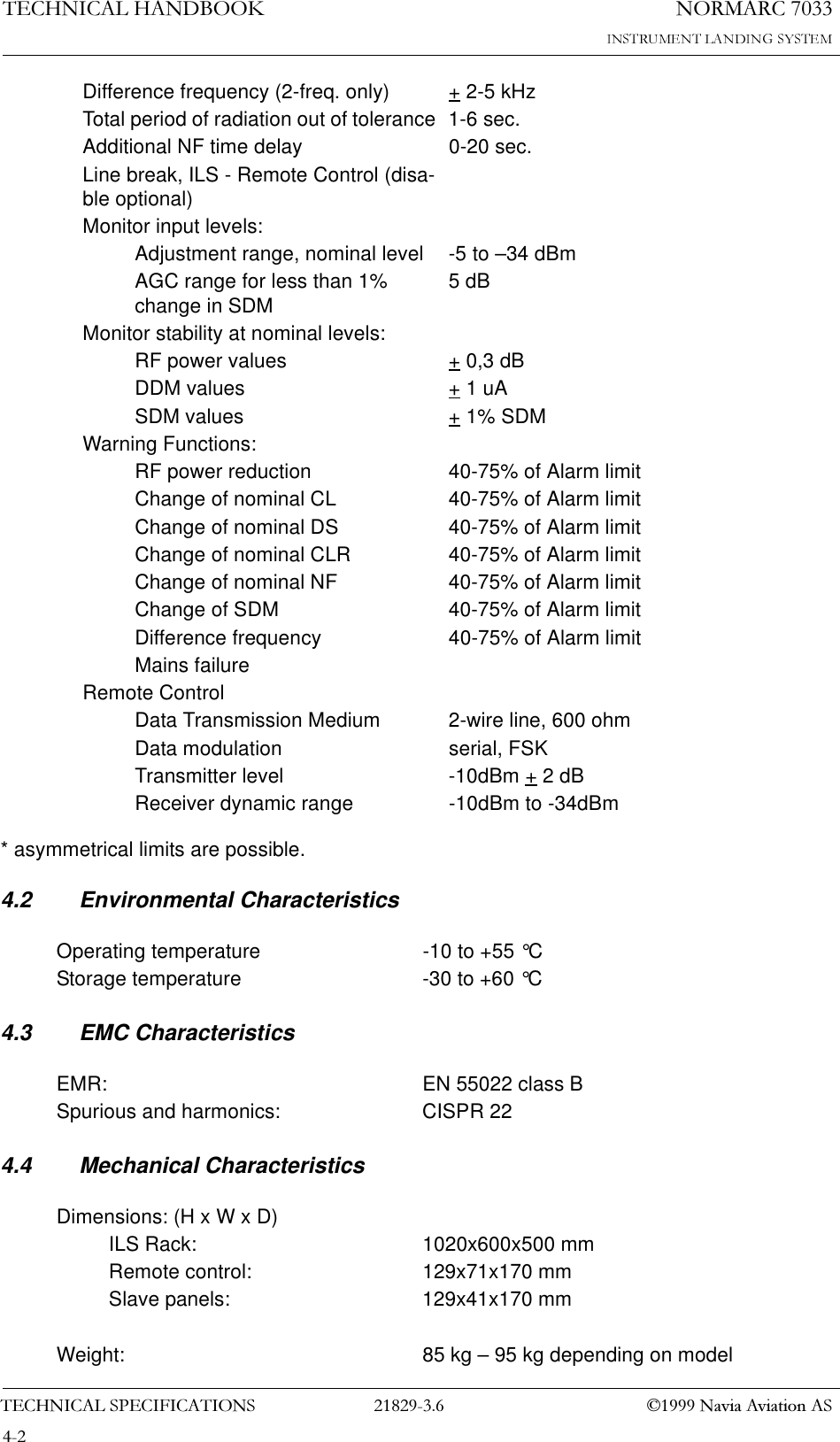
1250$5&7(&+1,&$/+$1'%22.7(&+1,&$/63(&,),&$7,216  1DYLD$YLDWLRQ$6* asymmetrical limits are possible.4.2 Environmental Characteristics4.3 EMC Characteristics4.4 Mechanical CharacteristicsDifference frequency (2-freq. only) + 2-5 kHzTotal period of radiation out of tolerance  1-6 sec.Additional NF time delay 0-20 sec.Line break, ILS - Remote Control (disa-ble optional)Monitor input levels:Adjustment range, nominal level -5 to –34 dBmAGC range for less than 1% change in SDM 5 dBMonitor stability at nominal levels:RF power values + 0,3 dBDDM values + 1 uASDM values + 1% SDMWarning Functions:RF power reduction 40-75% of Alarm limitChange of nominal CL 40-75% of Alarm limitChange of nominal DS 40-75% of Alarm limitChange of nominal CLR 40-75% of Alarm limitChange of nominal NF 40-75% of Alarm limitChange of SDM 40-75% of Alarm limitDifference frequency 40-75% of Alarm limitMains failureRemote ControlData Transmission Medium 2-wire line, 600 ohmData modulation serial, FSKTransmitter level -10dBm + 2 dBReceiver dynamic range -10dBm to -34dBmOperating temperature -10 to +55 °CStorage temperature -30 to +60 °CEMR: EN 55022 class BSpurious and harmonics: CISPR 22Dimensions: (H x W x D)ILS Rack: 1020x600x500 mmRemote control: 129x71x170 mmSlave panels: 129x41x170 mmWeight: 85 kg – 95 kg depending on model
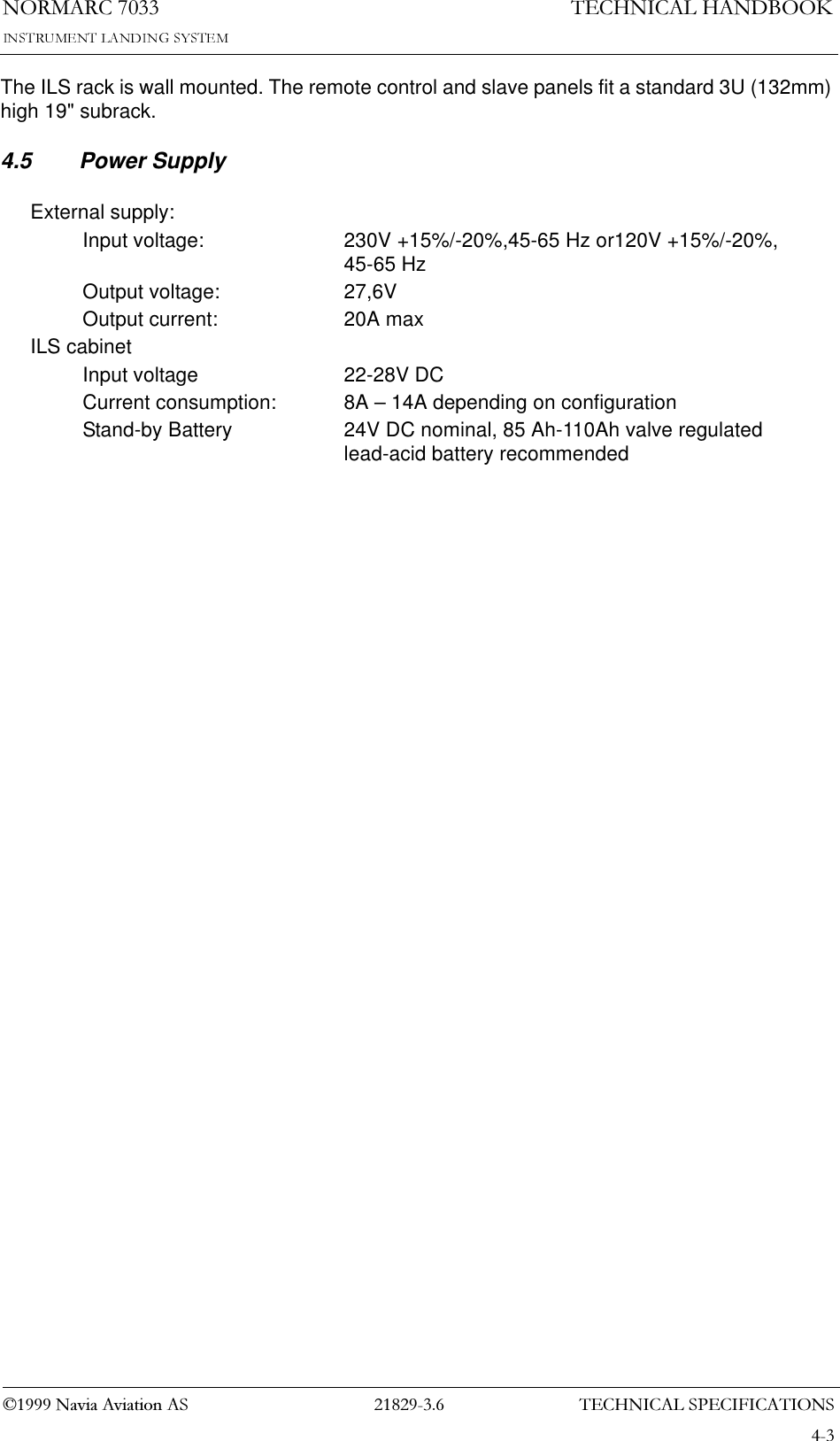
7(&+1,&$/63(&,),&$7,2161250$5&1DYLD$YLDWLRQ$67(&+1,&$/+$1'%22.The ILS rack is wall mounted. The remote control and slave panels fit a standard 3U (132mm) high 19" subrack.4.5 Power SupplyExternal supply:Input voltage: 230V +15%/-20%,45-65 Hz or120V +15%/-20%, 45-65 HzOutput voltage: 27,6VOutput current: 20A maxILS cabinetInput voltage 22-28V DCCurrent consumption: 8A – 14A depending on configurationStand-by Battery 24V DC nominal, 85 Ah-110Ah valve regulated lead-acid battery recommended
1250$5&7(&+1,&$/+$1'%22.7(&+1,&$/63(&,),&$7,216  1DYLD$YLDWLRQ$6
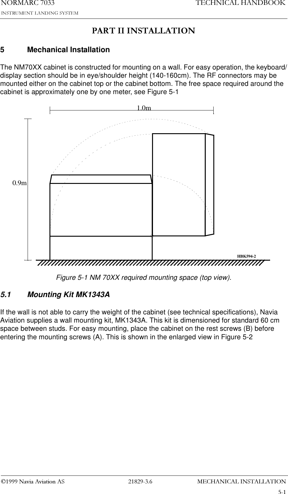
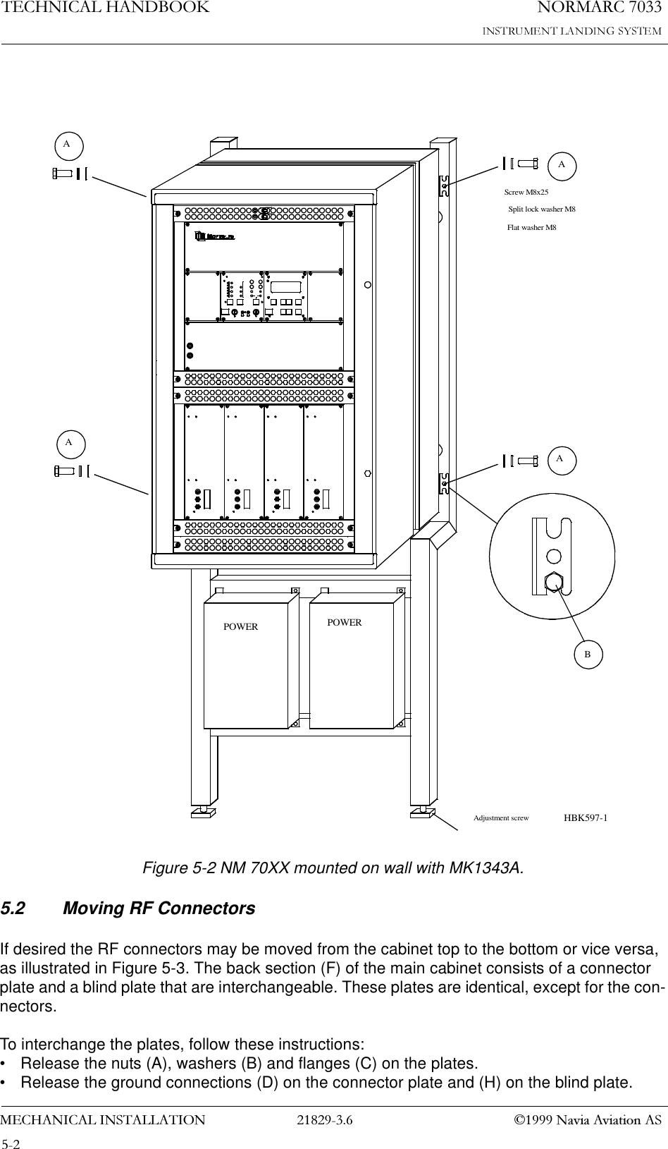
0(&+$1,&$/,167$//$7,211250$5&1DYLD$YLDWLRQ$67(&+1,&$/+$1'%22.3$57,,,167$//$7,215 Mechanical InstallationThe NM70XX cabinet is constructed for mounting on a wall. For easy operation, the keyboard/display section should be in eye/shoulder height (140-160cm). The RF connectors may be mounted either on the cabinet top or the cabinet bottom. The free space required around the cabinet is approximately one by one meter, see Figure 5-1Figure 5-1 NM 70XX required mounting space (top view).5.1 Mounting Kit MK1343AIf the wall is not able to carry the weight of the cabinet (see technical specifications), Navia Aviation supplies a wall mounting kit, MK1343A. This kit is dimensioned for standard 60 cm space between studs. For easy mounting, place the cabinet on the rest screws (B) before entering the mounting screws (A). This is shown in the enlarged view in Figure 5-20.9m1.0mHBK594-2
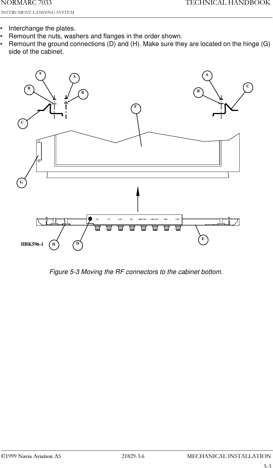
1250$5&7(&+1,&$/+$1'%22.0(&+$1,&$/,167$//$7,21  1DYLD$YLDWLRQ$6Figure 5-2 NM 70XX mounted on wall with MK1343A.5.2 Moving RF ConnectorsIf desired the RF connectors may be moved from the cabinet top to the bottom or vice versa, as illustrated in Figure 5-3. The back section (F) of the main cabinet consists of a connector plate and a blind plate that are interchangeable. These plates are identical, except for the con-nectors. To interchange the plates, follow these instructions:• Release the nuts (A), washers (B) and flanges (C) on the plates.• Release the ground connections (D) on the connector plate and (H) on the blind plate.POWER POWERAdjustment screw11Flat washer M8Split lock washer M8Screw M8x25BAAAAHBK597-1
0(&+$1,&$/,167$//$7,211250$5&1DYLD$YLDWLRQ$67(&+1,&$/+$1'%22.• Interchange the plates.• Remount the nuts, washers and flanges in the order shown.• Remount the ground connections (D) and (H). Make sure they are located on the hinge (G) side of the cabinet.Figure 5-3 Moving the RF connectors to the cabinet bottom.CLDNFCABABCSB CLRCLR DS SBO CLRESBO CSBAFBCGHHBK596-1
1250$5&7(&+1,&$/+$1'%22.0(&+$1,&$/,167$//$7,21  1DYLD$YLDWLRQ$6
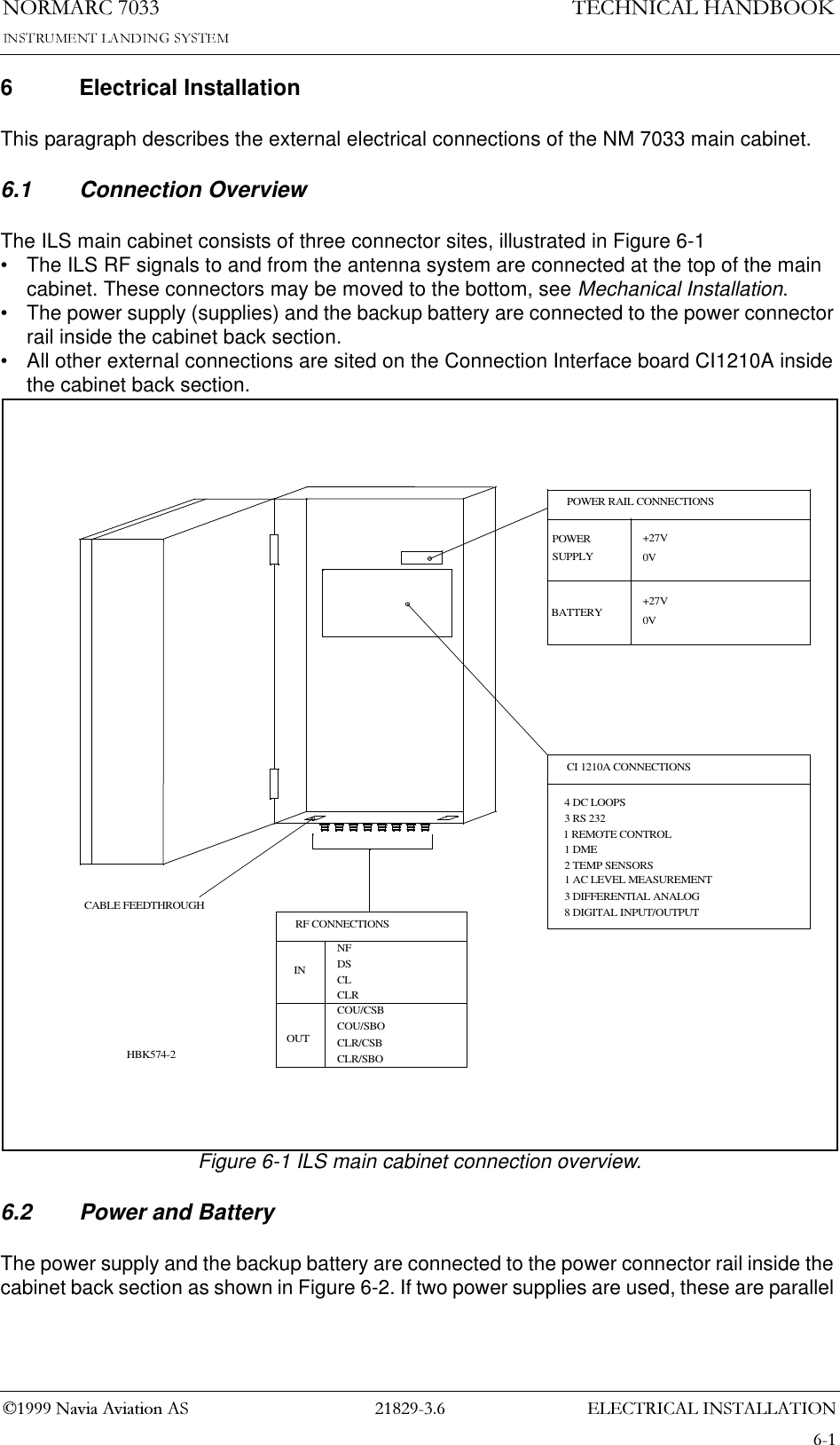
(/(&75,&$/,167$//$7,211250$5&1DYLD$YLDWLRQ$67(&+1,&$/+$1'%22.6 Electrical InstallationThis paragraph describes the external electrical connections of the NM 7033 main cabinet.6.1 Connection OverviewThe ILS main cabinet consists of three connector sites, illustrated in Figure 6-1• The ILS RF signals to and from the antenna system are connected at the top of the main cabinet. These connectors may be moved to the bottom, see Mechanical Installation.• The power supply (supplies) and the backup battery are connected to the power connector rail inside the cabinet back section.• All other external connections are sited on the Connection Interface board CI1210A inside the cabinet back section. Figure 6-1 ILS main cabinet connection overview.6.2 Power and BatteryThe power supply and the backup battery are connected to the power connector rail inside the cabinet back section as shown in Figure 6-2. If two power supplies are used, these are parallel RF CONNECTIONSCABLE FEEDTHROUGHCOU/SBOCLR/SBOCLR/CSBOUTCOU/CSBCLRDSNFIN CL1 AC LEVEL MEASUREMENTCI 1210A CONNECTIONS8 DIGITAL INPUT/OUTPUT3 DIFFERENTIAL ANALOG2 TEMP SENSORS1 DME1 REMOTE CONTROL3 RS 2324 DC LOOPSBATTERY +27V0VPOWER RAIL CONNECTIONSSUPPLYPOWER +27V0VHBK574-2
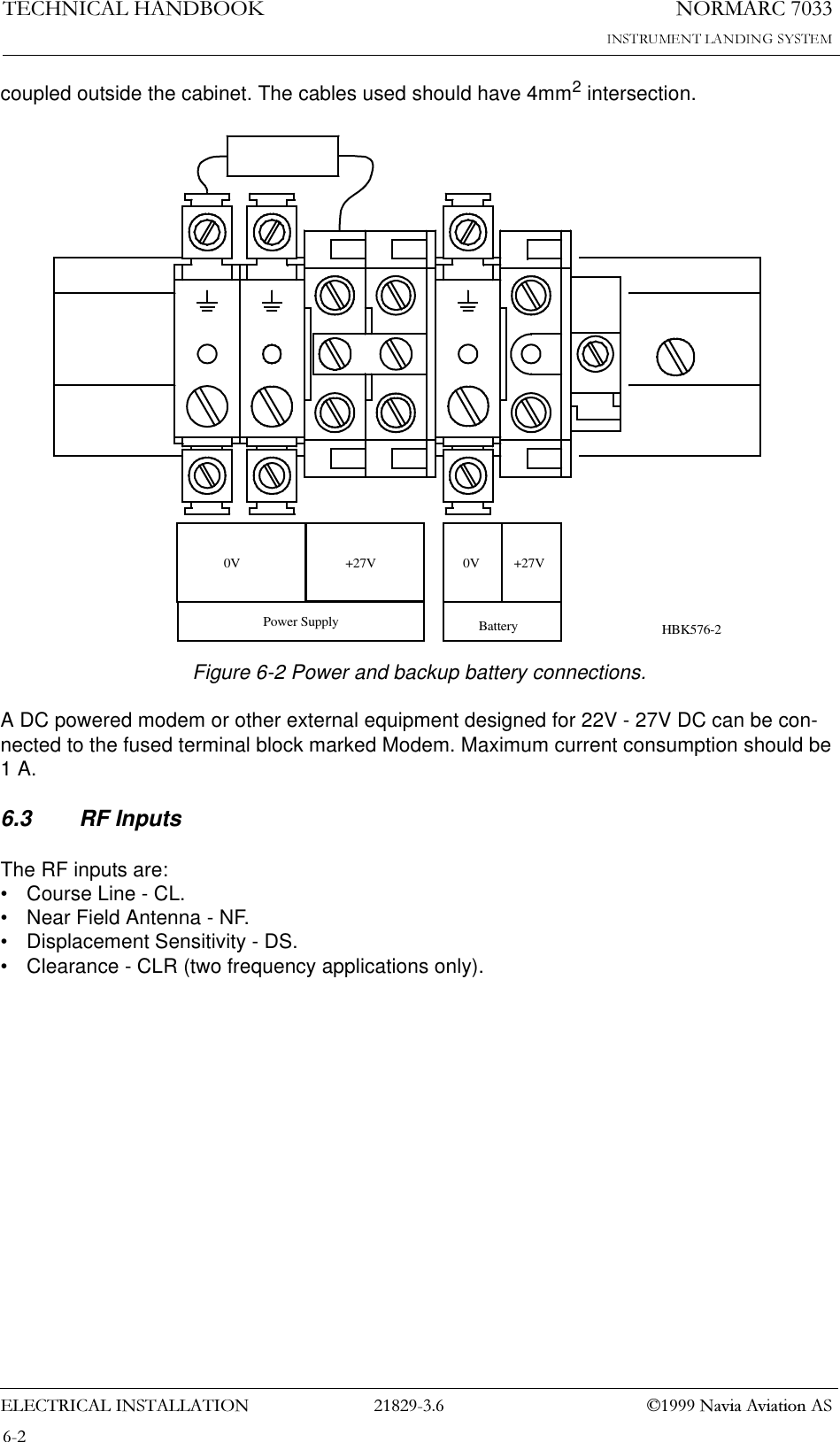
1250$5&7(&+1,&$/+$1'%22.(/(&75,&$/,167$//$7,21  1DYLD$YLDWLRQ$6coupled outside the cabinet. The cables used should have 4mm2 intersection.Figure 6-2 Power and backup battery connections.A DC powered modem or other external equipment designed for 22V - 27V DC can be con-nected to the fused terminal block marked Modem. Maximum current consumption should be 1 A.6.3 RF InputsThe RF inputs are:• Course Line - CL.• Near Field Antenna - NF.• Displacement Sensitivity - DS.• Clearance - CLR (two frequency applications only).Battery0V +27VPower Supply0V +27VHBK576-2
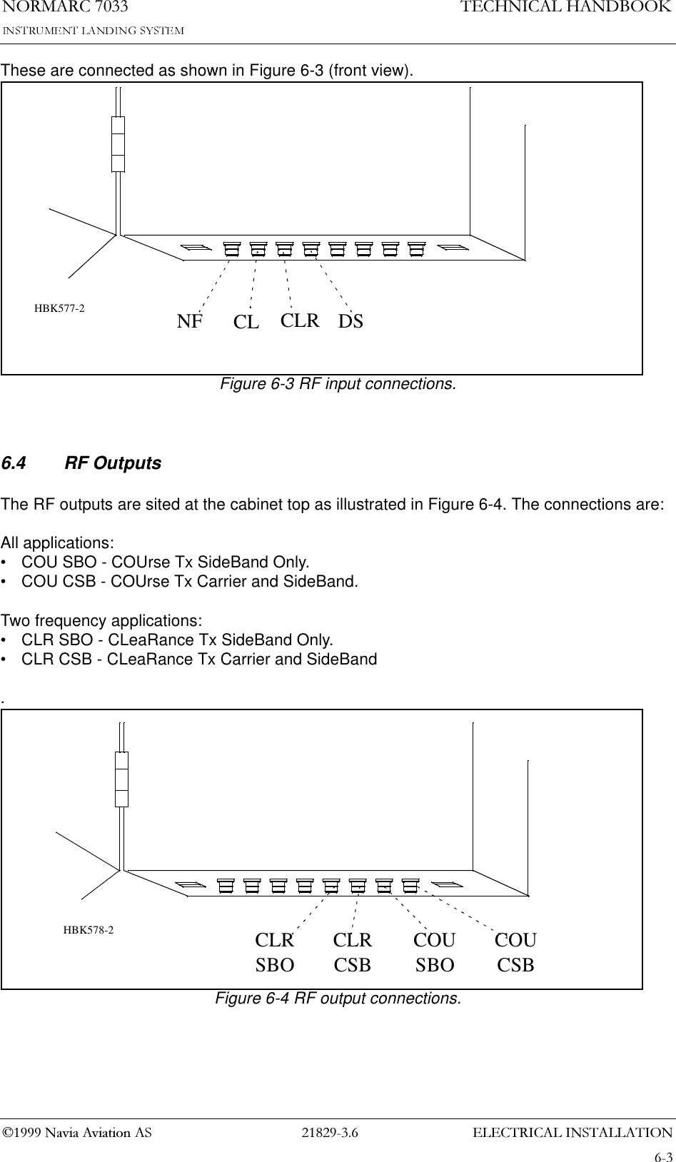
(/(&75,&$/,167$//$7,211250$5&1DYLD$YLDWLRQ$67(&+1,&$/+$1'%22.These are connected as shown in Figure 6-3 (front view).    Figure 6-3 RF input connections.6.4 RF OutputsThe RF outputs are sited at the cabinet top as illustrated in Figure 6-4. The connections are:All applications:• COU SBO - COUrse Tx SideBand Only.• COU CSB - COUrse Tx Carrier and SideBand.Two frequency applications:• CLR SBO - CLeaRance Tx SideBand Only.• CLR CSB - CLeaRance Tx Carrier and SideBand. Figure 6-4 RF output connections.NF CL CLR DSHBK577-2COUCSBCOUSBOCLRCSBCLRSBOHBK578-2
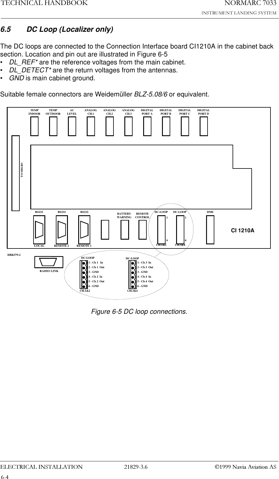
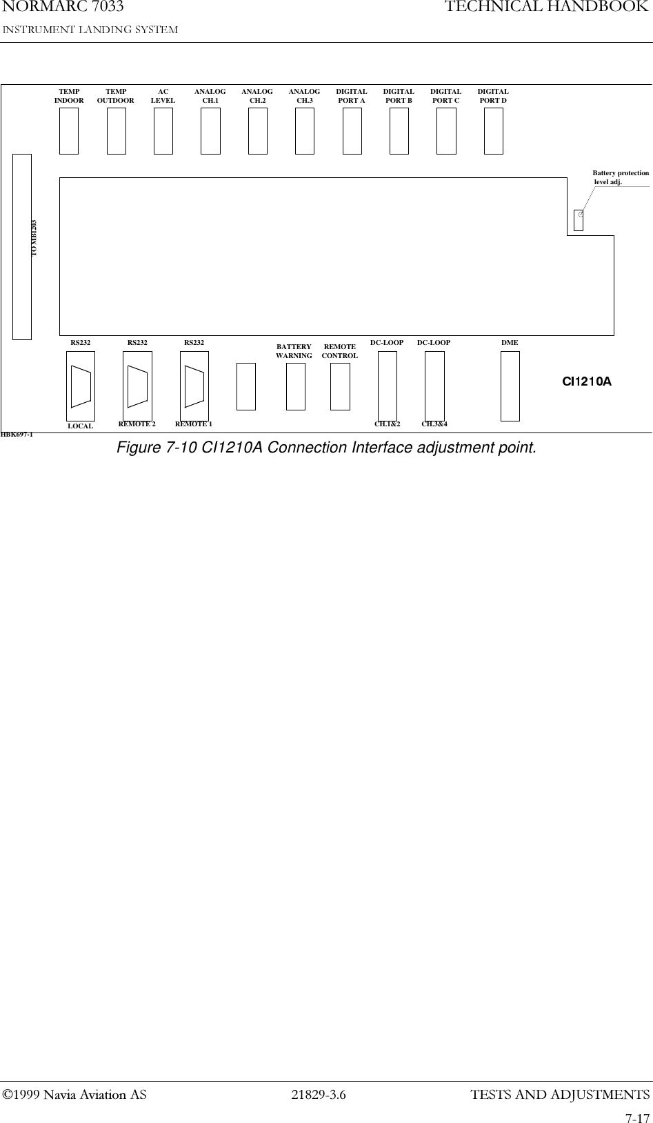
1250$5&7(&+1,&$/+$1'%22.(/(&75,&$/,167$//$7,21  1DYLD$YLDWLRQ$66.5 DC Loop (Localizer only)The DC loops are connected to the Connection Interface board CI1210A in the cabinet back section. Location and pin out are illustrated in Figure 6-5•DL_REF* are the reference voltages from the main cabinet.•DL_DETECT* are the return voltages from the antennas.•GND is main cabinet ground.Suitable female connectors are Weidemüller BLZ-5.08/6 or equivalent.Figure 6-5 DC loop connections. TEMPINDOOR TEMPOUTDOOR ACLEVEL ANALOGCH.1 ANALOGCH.2 ANALOGCH.3 DIGITALPORT A DIGITALPORT B DIGITALPORT C DIGITALPORT DTO MB1203RS232 RS232 RS232 REMOTECONTROLDC-LOOP DC-LOOP DMELOCAL REMOTE 2 REMOTE 1 CH.1&2 CH.3&416DC-LOOPCH.1&2DC-LOOPCH.3&41 - Ch 1   In2 - Ch 1  Out3 - GND4 - Ch 2  In5 - Ch 2  Out6 - GNDCI 1210A1 - Ch 3  In2 - Ch 3  Out3 - GND4 - Ch 4  In5 - Ch 4  Out6 - GND16BATTERYWARNINGHBK579-2RADIO LINK
(/(&75,&$/,167$//$7,211250$5&1DYLD$YLDWLRQ$67(&+1,&$/+$1'%22.6.6 Remote ControlThe remote control is connected to the Connection Interface board CI1210A as illustrated in Figure 6-6. The connection of the remote control, remote slave panel and interlock switch is done at the remote control site and covered in chapter 6.13 - 6.16•FSK_[P,N] is the modem line pair.•GND is main cabinet ground.For normal FSK modem operation the straps S9-11 on CI1210A should be mounted.A suitable female connector is Weidemüller BLZ-5.08/4 or equivalent.Figure 6-6 Remote control connection.TEMPINDOOR TEMPOUTDOOR ACLEVEL ANALOGCH.1 ANALOGCH.2 ANALOGCH.3 DIGITALPORT A DIGITALPORT B DIGITALPORT C DIGITALPORT DTO MB1203RS232 RS232 RS232 REMOTECONTROLDC-LOOP DC-LOOP DMELOCAL REMOTE 2 REMOTE 1 CH.1&2 CH.3&4REMOTECONTROL1 - GND2 - FSK_P3 - FSK_N4 - GND14S9-14BATTERYWARNINGHBK580-1RADIO LINK
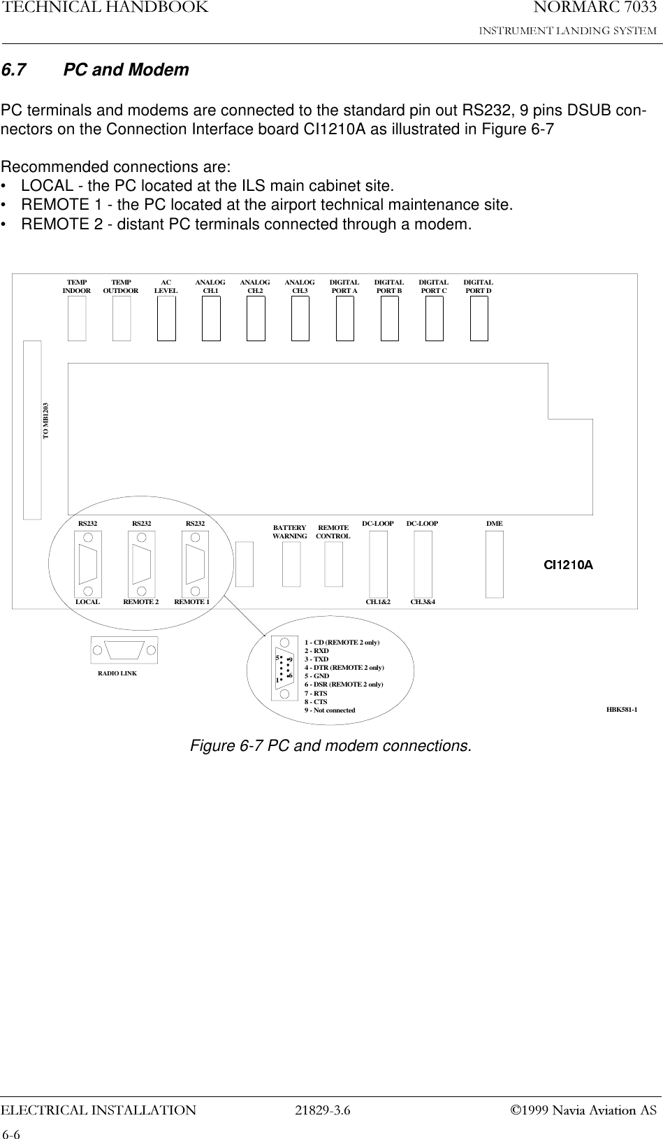
1250$5&7(&+1,&$/+$1'%22.(/(&75,&$/,167$//$7,21  1DYLD$YLDWLRQ$66.7 PC and ModemPC terminals and modems are connected to the standard pin out RS232, 9 pins DSUB con-nectors on the Connection Interface board CI1210A as illustrated in Figure 6-7Recommended connections are:• LOCAL - the PC located at the ILS main cabinet site.• REMOTE 1 - the PC located at the airport technical maintenance site.• REMOTE 2 - distant PC terminals connected through a modem.Figure 6-7 PC and modem connections.TEMPINDOOR TEMPOUTDOOR ACLEVEL ANALOGCH.1 ANALOGCH.2 ANALOGCH.3 DIGITALPORT A DIGITALPORT B DIGITALPORT C DIGITALPORT DTO MB1203RS232 RS232 RS232 REMOTECONTROLDC-LOOP DC-LOOP DMELOCAL REMOTE 2 REMOTE 1 CH.1&2 CH.3&415691 - CD (REMOTE 2 only)2 - RXD3 - TXD4 - DTR (REMOTE 2 only)5 - GND6 - DSR (REMOTE 2 only)7 - RTS8 - CTS9 - Not connectedBATTERYWARNINGHBK581-1RADIO LINK
(/(&75,&$/,167$//$7,211250$5&1DYLD$YLDWLRQ$67(&+1,&$/+$1'%22.6.8 DME (localizer only)Distance Measurement Equipment DME is connected to the Connection Interface board CI1210A as illustrated in Figure 6-8•ACT_DME[P,N] is the positive and negative terminal of the DME active signal from the DME, respectively.•IN_DME[P,N] is the positive and negative terminal of the morse code envelope signal from the DME, respectively.•OUT_DME[P,N] is the positive and negative terminal of the morse code envelope signal to the DME, respectively.A suitable female connector is Weidemüller BLZ-5.08/6 or equivalent.Figure 6-8 DME connections.TEMPINDOORTEMPOUTDOORACLEVELANALOGCH.1ANALOGCH.2ANALOGCH.3DIGITALPORT ADIGITALPORT BDIGITALPORT CDIGITALPORT DTO MB1203RS232 RS232 RS232 REMOTECONTROLDC-LOOP DC-LOOP DMELOCAL REMOTE 2 REMOTE 1 CH.1&2 CH.3&41 - ACT_DMEP2 - ACT_DMEN3 - IN_DMEP4 - IN_DMENCI1210A16S1-8DME5 - OUT_DMEP6 - OUT_DMENBATTERYWARNINGHBK582-1RADIO LINK
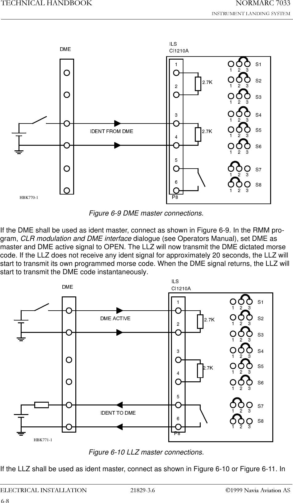
1250$5&7(&+1,&$/+$1'%22.(/(&75,&$/,167$//$7,21  1DYLD$YLDWLRQ$6Figure 6-9 DME master connections.If the DME shall be used as ident master, connect as shown in Figure 6-9. In the RMM pro-gram, CLR modulation and DME interface dialogue (see Operators Manual), set DME as master and DME active signal to OPEN. The LLZ will now transmit the DME dictated morse code. If the LLZ does not receive any ident signal for approximately 20 seconds, the LLZ will start to transmit its own programmed morse code. When the DME signal returns, the LLZ will start to transmit the DME code instantaneously.Figure 6-10 LLZ master connections.If the LLZ shall be used as ident master, connect as shown in Figure 6-10 or Figure 6-11. In HBK770-1HBK771-1
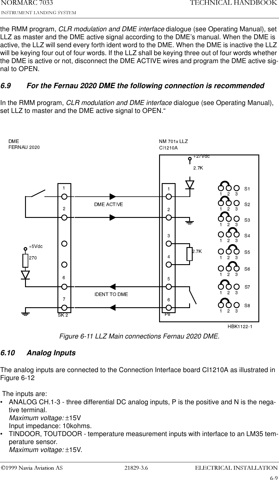
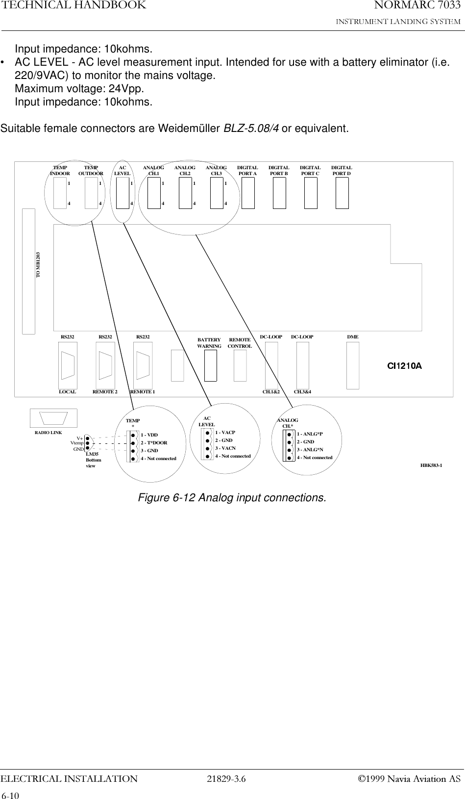
(/(&75,&$/,167$//$7,211250$5&1DYLD$YLDWLRQ$67(&+1,&$/+$1'%22.the RMM program, CLR modulation and DME interface dialogue (see Operating Manual), set LLZ as master and the DME active signal according to the DME’s manual. When the DME is active, the LLZ will send every forth ident word to the DME. When the DME is inactive the LLZ will be keying four out of four words. If the LLZ shall be keying three out of four words whether the DME is active or not, disconnect the DME ACTIVE wires and program the DME active sig-nal to OPEN.6.9 For the Fernau 2020 DME the following connection is recommendedIn the RMM program, CLR modulation and DME interface dialogue (see Operating Manual), set LLZ to master and the DME active signal to OPEN.“Figure 6-11 LLZ Main connections Fernau 2020 DME.6.10 Analog InputsThe analog inputs are connected to the Connection Interface board CI1210A as illustrated in Figure 6-12 The inputs are:• ANALOG CH.1-3 - three differential DC analog inputs, P is the positive and N is the nega-tive terminal.Maximum voltage: ±15VInput impedance: 10kohms.• TINDOOR, TOUTDOOR - temperature measurement inputs with interface to an LM35 tem-perature sensor.Maximum voltage: ±15V.
1250$5&7(&+1,&$/+$1'%22.(/(&75,&$/,167$//$7,21  1DYLD$YLDWLRQ$6Input impedance: 10kohms.• AC LEVEL - AC level measurement input. Intended for use with a battery eliminator (i.e. 220/9VAC) to monitor the mains voltage.Maximum voltage: 24Vpp.Input impedance: 10kohms.Suitable female connectors are Weidemüller BLZ-5.08/4 or equivalent.Figure 6-12 Analog input connections.TEMPINDOOR TEMPOUTDOOR ACLEVEL ANALOGCH.1 ANALOGCH.2 ANALOGCH.3 DIGITALPORT A DIGITALPORT B DIGITALPORT C DIGITALPORT DTO MB1203RS232 RS232 RS232 REMOTECONTROLDC-LOOP DC-LOOP DMELOCAL REMOTE 2 REMOTE 1 CH.1&2 CH.3&4TEMP*1 - VDD2 - T*DOOR3 - GND4 - Not connected14LM35Bottomview1 - VACP2 - GND3 - VACN4 - Not connectedACLEVEL1 - ANLG*P2 - GND3 - ANLG*N4 - Not connectedANALOGCH.*1414141414V+VtempGNDBATTERYWARNINGHBK583-1RADIO LINK
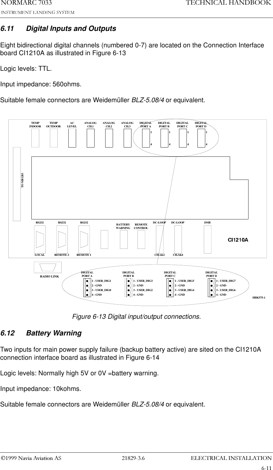
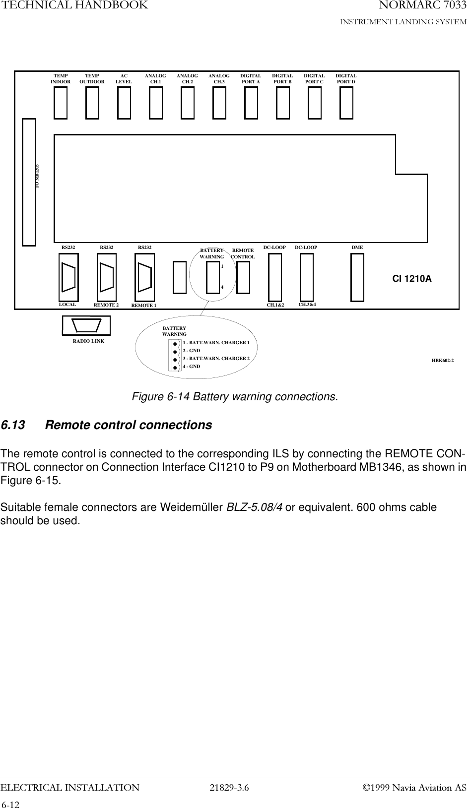
(/(&75,&$/,167$//$7,211250$5&1DYLD$YLDWLRQ$67(&+1,&$/+$1'%22.6.11 Digital Inputs and OutputsEight bidirectional digital channels (numbered 0-7) are located on the Connection Interface board CI1210A as illustrated in Figure 6-13Logic levels: TTL.Input impedance: 560ohms.Suitable female connectors are Weidemüller BLZ-5.08/4 or equivalent.Figure 6-13 Digital input/output connections.6.12 Battery WarningTwo inputs for main power supply failure (backup battery active) are sited on the CI1210A connection interface board as illustrated in Figure 6-14Logic levels: Normally high 5V or 0V =battery warning.Input impedance: 10kohms.Suitable female connectors are Weidemüller BLZ-5.08/4 or equivalent.TEMPINDOOR TEMPOUTDOOR ACLEVEL ANALOGCH.1 ANALOGCH.2 ANALOGCH.3 DIGITALPORT A DIGITALPORT B DIGITALPORT C DIGITALPORT DTO MB1203RS232 RS232 RS232 REMOTECONTROLDC-LOOP DC-LOOP DMELOCAL REMOTE 2 REMOTE 1 CH.1&2 CH.3&41 - USER_DIG52 - GND3 - USER_DIG44 - GND14141414DIGITALPORT C1 - USER_DIG32 - GND3 - USER_DIG24 - GNDDIGITALPORT B1 - USER_DIG12 - GND3 - USER_DIG04 - GNDDIGITALPORT A1 - USER_DIG72 - GND3 - USER_DIG64 - GNDDIGITALPORT DBATTERYWARNINGHBK575-1RADIO LINK
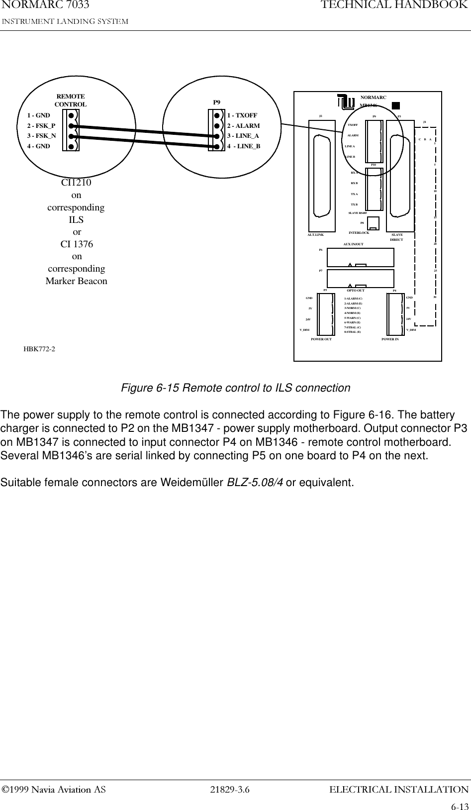
1250$5&7(&+1,&$/+$1'%22.(/(&75,&$/,167$//$7,21  1DYLD$YLDWLRQ$6Figure 6-14 Battery warning connections.6.13 Remote control connectionsThe remote control is connected to the corresponding ILS by connecting the REMOTE CON-TROL connector on Connection Interface CI1210 to P9 on Motherboard MB1346, as shown in Figure 6-15.Suitable female connectors are Weidemüller BLZ-5.08/4 or equivalent. 600 ohms cable should be used.TEMPINDOOR TEMPOUTDOOR ACLEVEL ANALOGCH.1 ANALOGCH.2 ANALOGCH.3 DIGITALPORT A DIGITALPORT B DIGITALPORT C DIGITALPORT DTO MB1203RS232 RS232 RS232 REMOTECONTROLDC-LOOP DC-LOOP DMELOCAL REMOTE 2 REMOTE 1 CH.1&2 CH.3&4BATTERYWARNING1 - BATT.WARN. CHARGER 12 - GND3 - BATT.WARN. CHARGER 24 - GNDCI 1210A14BATTERYWARNINGHBK602-2RADIO LINK
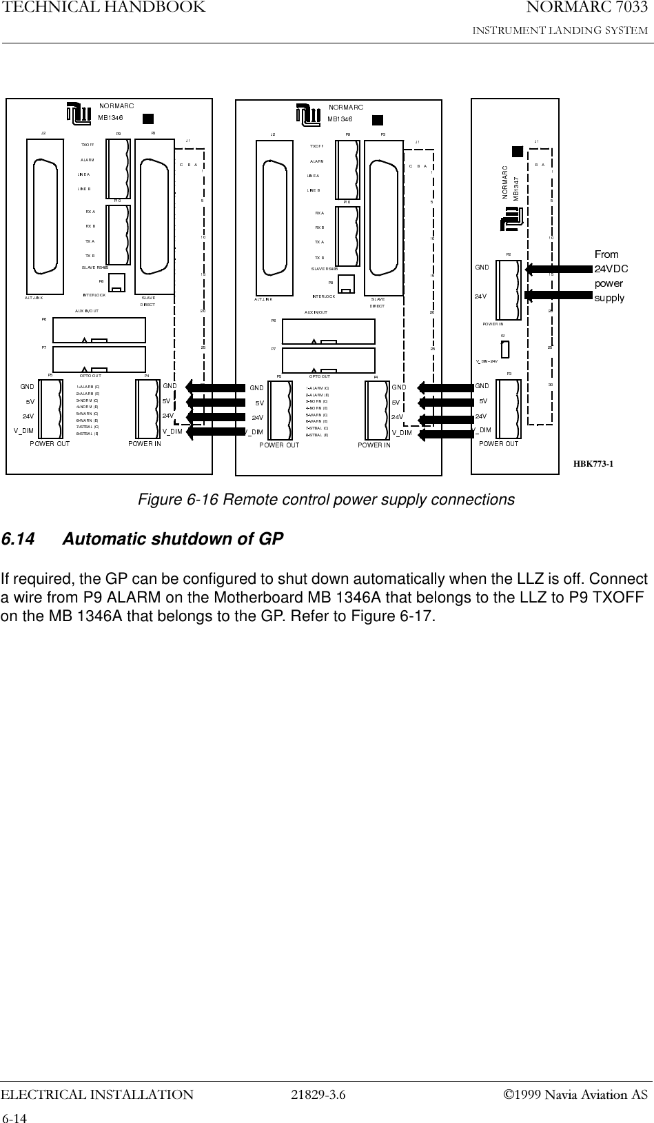
(/(&75,&$/,167$//$7,211250$5&1DYLD$YLDWLRQ$67(&+1,&$/+$1'%22.Figure 6-15 Remote control to ILS connectionThe power supply to the remote control is connected according to Figure 6-16. The battery charger is connected to P2 on the MB1347 - power supply motherboard. Output connector P3 on MB1347 is connected to input connector P4 on MB1346 - remote control motherboard. Several MB1346’s are serial linked by connecting P5 on one board to P4 on the next.Suitable female connectors are Weidemüller BLZ-5.08/4 or equivalent.REMOTECONTROL1 - GND2 - FSK_P3 - FSK_N4 - GNDJ2 P3P6P7P4P5P9P10P8NORMARCOPTO OUT2-ALARM (E)1-ALARM (C)4-NORM (E)5-WARN (C)6-WARN (E)7-STBAL (C)8-STBAL (E)3-NORM (C)GND5V24VV_DIMGND5V24VV_DIMPOWER OUT POWER INAUX IN/OUTSLAVEDIRECTINTERLOCKTXOFFALARMLINE ALINE BRX ARX BTX ATX BSLAVE RS485J1ABC153020251510ALT.LINKMB1346P91 - TXOFF2 - ALARM3 - LINE_A4  - LINE_BCI1210 on corresponding ILSorCI 1376oncorrespondingMarker BeaconHBK772-2
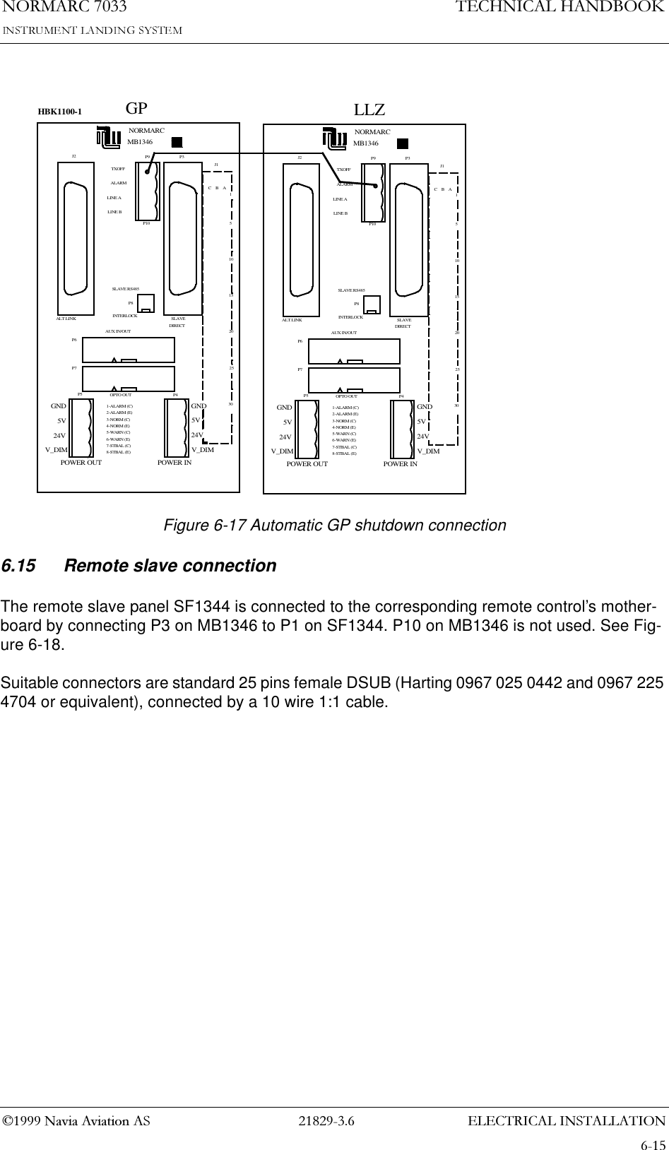
1250$5&7(&+1,&$/+$1'%22.(/(&75,&$/,167$//$7,21  1DYLD$YLDWLRQ$6Figure 6-16 Remote control power supply connections6.14 Automatic shutdown of GPIf required, the GP can be configured to shut down automatically when the LLZ is off. Connect a wire from P9 ALARM on the Motherboard MB 1346A that belongs to the LLZ to P9 TXOFF on the MB 1346A that belongs to the GP. Refer to Figure 6-17.HBK773-1
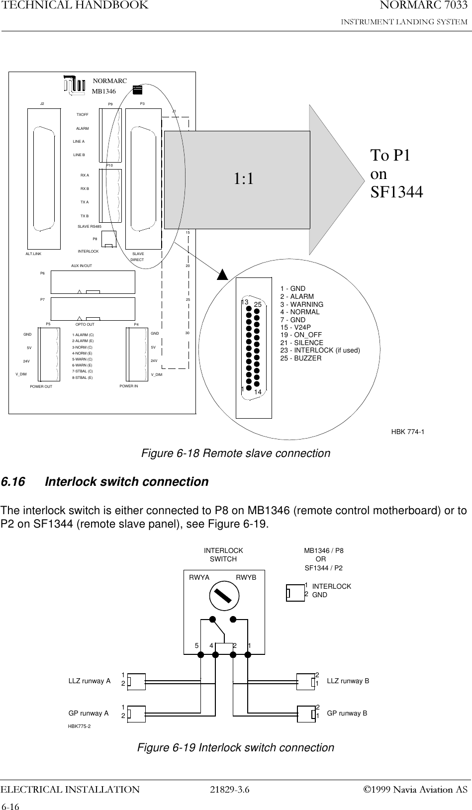
(/(&75,&$/,167$//$7,211250$5&1DYLD$YLDWLRQ$67(&+1,&$/+$1'%22.Figure 6-17 Automatic GP shutdown connection6.15 Remote slave connectionThe remote slave panel SF1344 is connected to the corresponding remote control’s mother-board by connecting P3 on MB1346 to P1 on SF1344. P10 on MB1346 is not used. See Fig-ure 6-18.Suitable connectors are standard 25 pins female DSUB (Harting 0967 025 0442 and 0967 225 4704 or equivalent), connected by a 10 wire 1:1 cable.J2 P3P6P7P4P5P9P10P8NORMARCOPTO OUT2-ALARM (E)1-ALARM (C)4-NORM (E)5-WARN (C)6-WARN (E)7-STBAL (C)8-STBAL (E)3-NORM (C)GND5V24VV_DIMGND5V24VV_DIMPOWER OUT POWER INAUX IN/OUTSLAVEDIRECTINTERLOCKTXOFFALARMLINE ALINE BSLAVE RS485J1ABC153020251510ALT.LINKMB1346J2 P3P6P7P4P5P9P10P8NORMARCOPTO OUT2-ALARM (E)1-ALARM (C)4-NORM (E)5-WARN (C)6-WARN (E)7-STBAL (C)8-STBAL (E)3-NORM (C)GND5V24VV_DIMGND5V24VV_DIMPOWER OUT POWER INAUX IN/OUTSLAVEDIRECTINTERLOCKTXOFFALARMLINE ALINE BSLAVE RS485J1ABC153020251510ALT.LINKMB1346GP LLZHBK1100-1
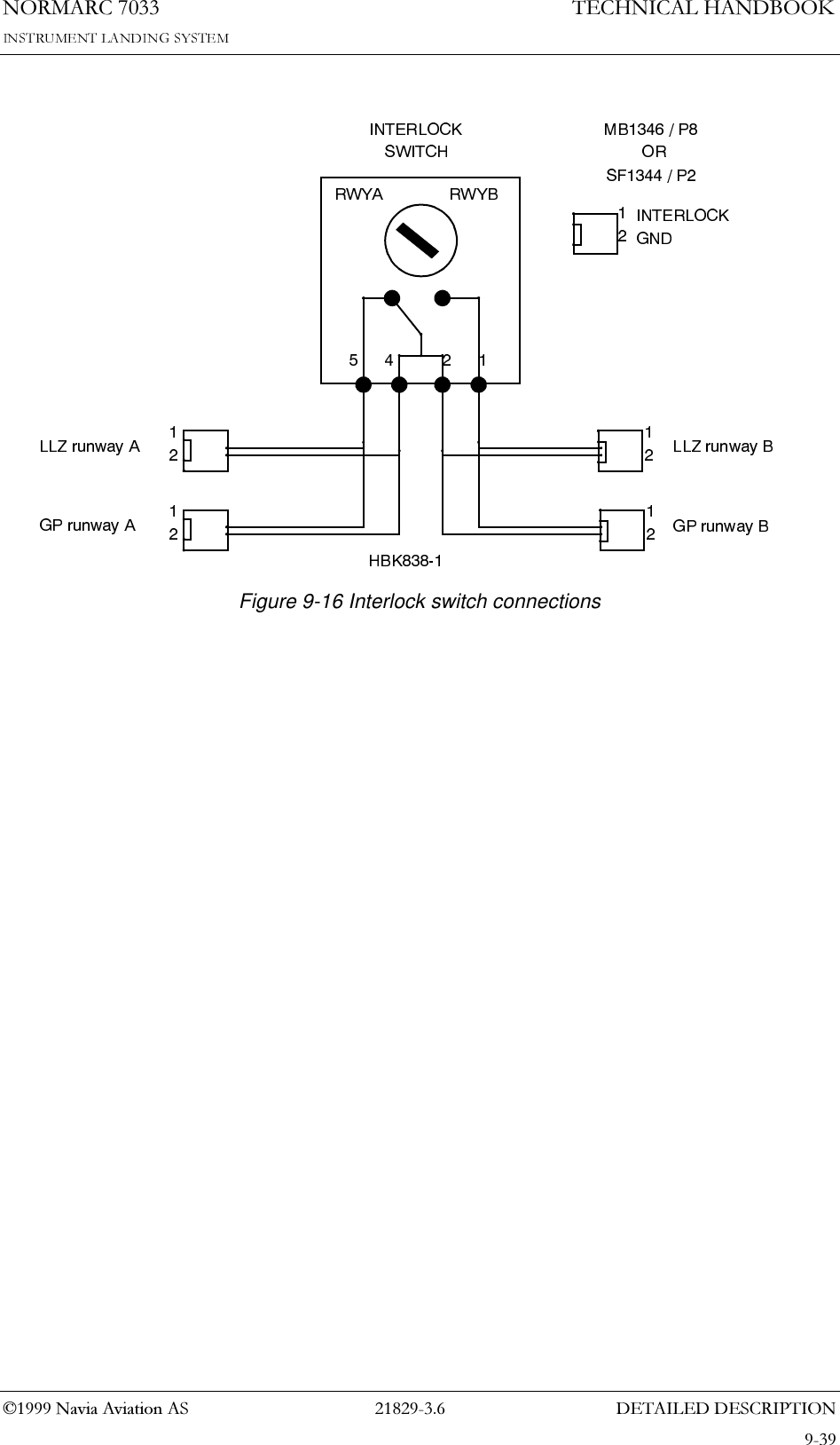
1250$5&7(&+1,&$/+$1'%22.(/(&75,&$/,167$//$7,21  1DYLD$YLDWLRQ$6Figure 6-18 Remote slave connection6.16 Interlock switch connectionThe interlock switch is either connected to P8 on MB1346 (remote control motherboard) or to P2 on SF1344 (remote slave panel), see Figure 6-19.Figure 6-19 Interlock switch connectionJ2 P3P6P7P4P5P9P10P8NORMARCOPTO OUT2-ALARM (E)1-ALARM (C)4-NORM (E)5-WARN (C)6-WARN (E)7-STBAL (C)8-STBAL (E)3-NORM (C)GND5V24VV_DIMGND5V24VV_DIMPOWER OUT POWER INAUX IN/OUTSLAVEDIRECTINTERLOCKTXOFFALARMLINE ALINE BRX ARX BTX ATX BSLAVE RS485J1ABC153020251510ALT.LINKMB1346To P1 onSF134411314251 - GND2 - ALARM3 - WARNING4 - NORMAL7 - GND15 - V24P19 - ON_OFF21 - SILENCE23 - INTERLOCK (if used)25 - BUZZER1:1HBK 774-121MB1346 / P8ORSF1344 / P2INTERLOCK SWITCHRWYA RWYB211212INTERLOCKGND1254 21LLZ runway AGP runway ALLZ runway BGP runway BHBK775-2
(/(&75,&$/,167$//$7,211250$5&1DYLD$YLDWLRQ$67(&+1,&$/+$1'%22.Note:When MB1346A is used with Remote Control Assembly RCA1240C or D and Interlock func-tion is not used (connected), a jumper plug must be installed in P8 (or P2).
1250$5&7(&+1,&$/+$1'%22.(/(&75,&$/,167$//$7,21  1DYLD$YLDWLRQ$6
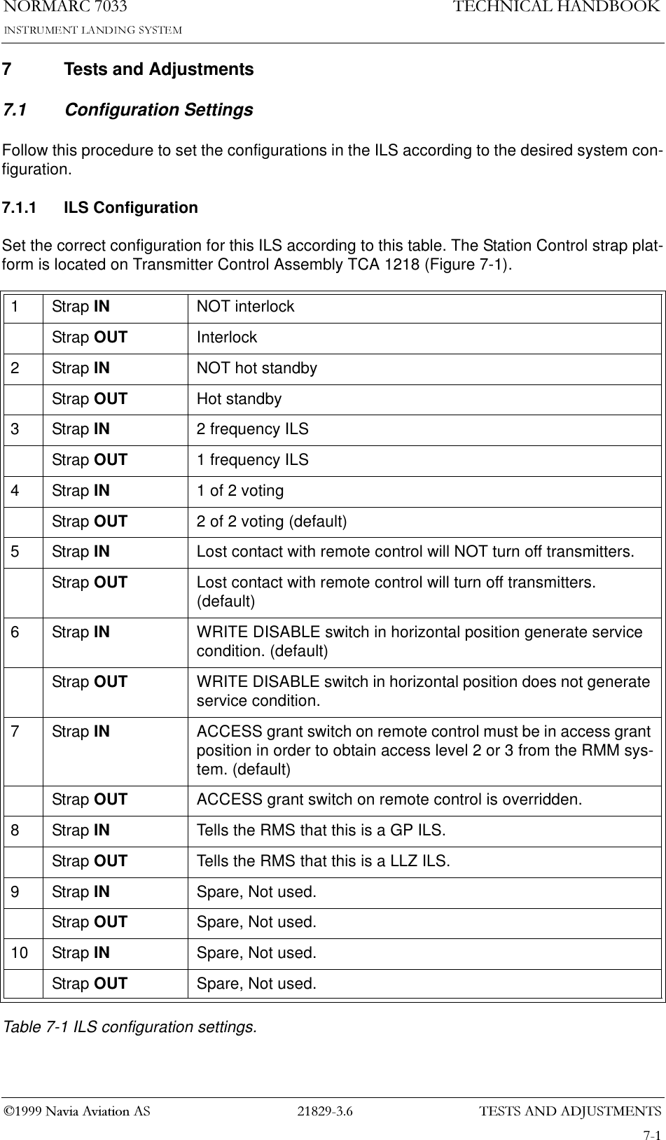
7(676$1'$'-8670(1761250$5&1DYLD$YLDWLRQ$67(&+1,&$/+$1'%22.7 Tests and Adjustments7.1 Configuration SettingsFollow this procedure to set the configurations in the ILS according to the desired system con-figuration.7.1.1 ILS ConfigurationSet the correct configuration for this ILS according to this table. The Station Control strap plat-form is located on Transmitter Control Assembly TCA 1218 (Figure 7-1).Table 7-1 ILS configuration settings.1 Strap IN NOT interlockStrap OUT Interlock2 Strap IN NOT hot standbyStrap OUT Hot standby3 Strap IN 2 frequency ILSStrap OUT 1 frequency ILS4 Strap IN 1 of 2 votingStrap OUT 2 of 2 voting (default)5 Strap IN Lost contact with remote control will NOT turn off transmitters.Strap OUT Lost contact with remote control will turn off transmitters. (default)6 Strap IN WRITE DISABLE switch in horizontal position generate service condition. (default)Strap OUT WRITE DISABLE switch in horizontal position does not generate service condition.7 Strap IN ACCESS grant switch on remote control must be in access grant position in order to obtain access level 2 or 3 from the RMM sys-tem. (default)Strap OUT ACCESS grant switch on remote control is overridden.8 Strap IN Tells the RMS that this is a GP ILS.Strap OUT Tells the RMS that this is a LLZ ILS.9 Strap IN Spare, Not used.Strap OUT Spare, Not used.10 Strap IN Spare, Not used.Strap OUT Spare, Not used.
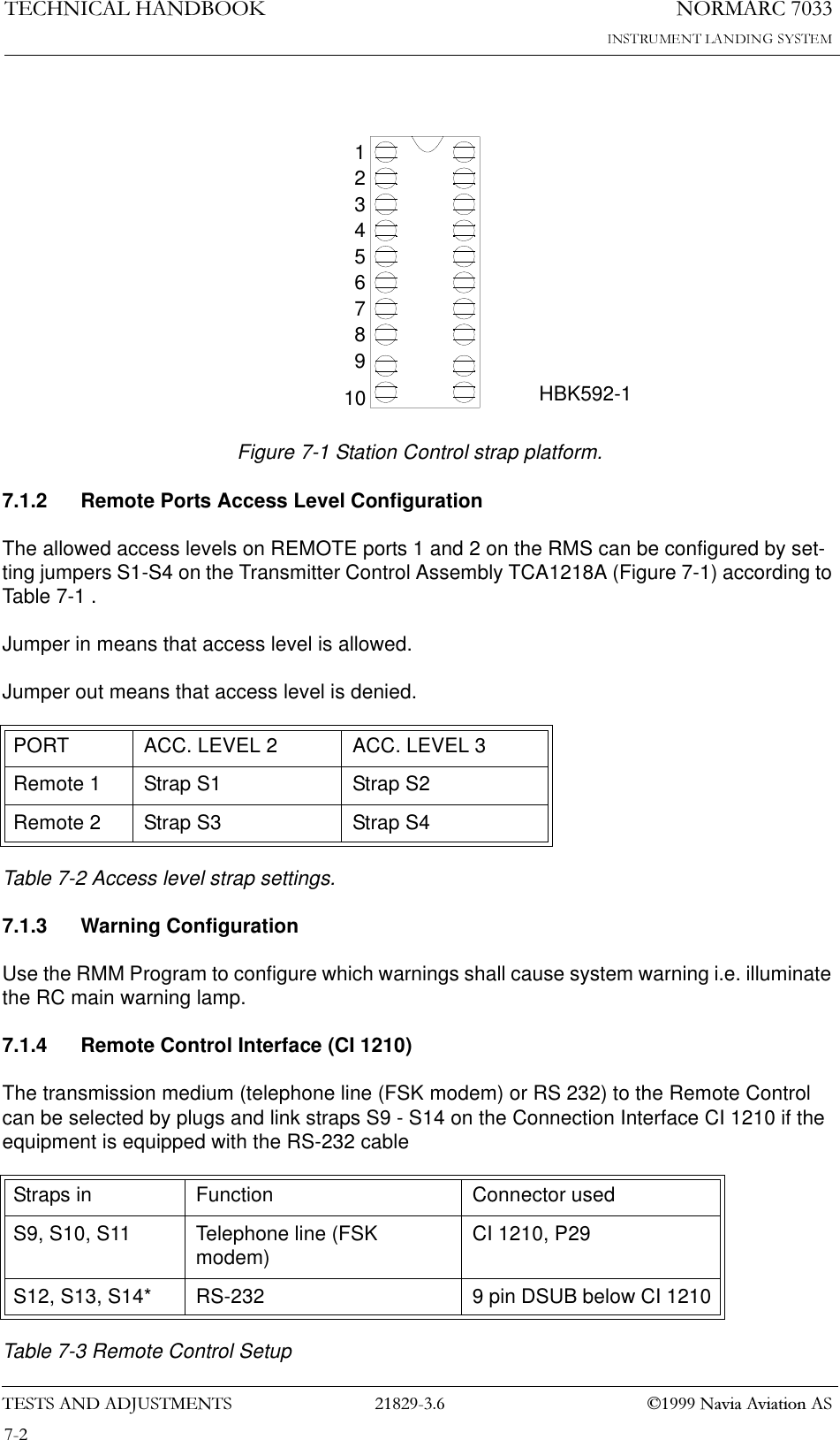
1250$5&7(&+1,&$/+$1'%22.7(676$1'$'-8670(176  1DYLD$YLDWLRQ$6Figure 7-1 Station Control strap platform.7.1.2 Remote Ports Access Level ConfigurationThe allowed access levels on REMOTE ports 1 and 2 on the RMS can be configured by set-ting jumpers S1-S4 on the Transmitter Control Assembly TCA1218A (Figure 7-1) according to Table 7-1 .Jumper in means that access level is allowed.Jumper out means that access level is denied.Table 7-2 Access level strap settings.7.1.3 Warning Configuration Use the RMM Program to configure which warnings shall cause system warning i.e. illuminate the RC main warning lamp.7.1.4 Remote Control Interface (CI 1210)The transmission medium (telephone line (FSK modem) or RS 232) to the Remote Control can be selected by plugs and link straps S9 - S14 on the Connection Interface CI 1210 if the equipment is equipped with the RS-232 cable Table 7-3 Remote Control SetupPORT ACC. LEVEL 2 ACC. LEVEL 3Remote 1 Strap S1 Strap S2Remote 2 Strap S3 Strap S4Straps in Function Connector usedS9, S10, S11 Telephone line (FSK modem) CI 1210, P29S12, S13, S14* RS-232 9 pin DSUB below CI 121012345678910 HBK592-1
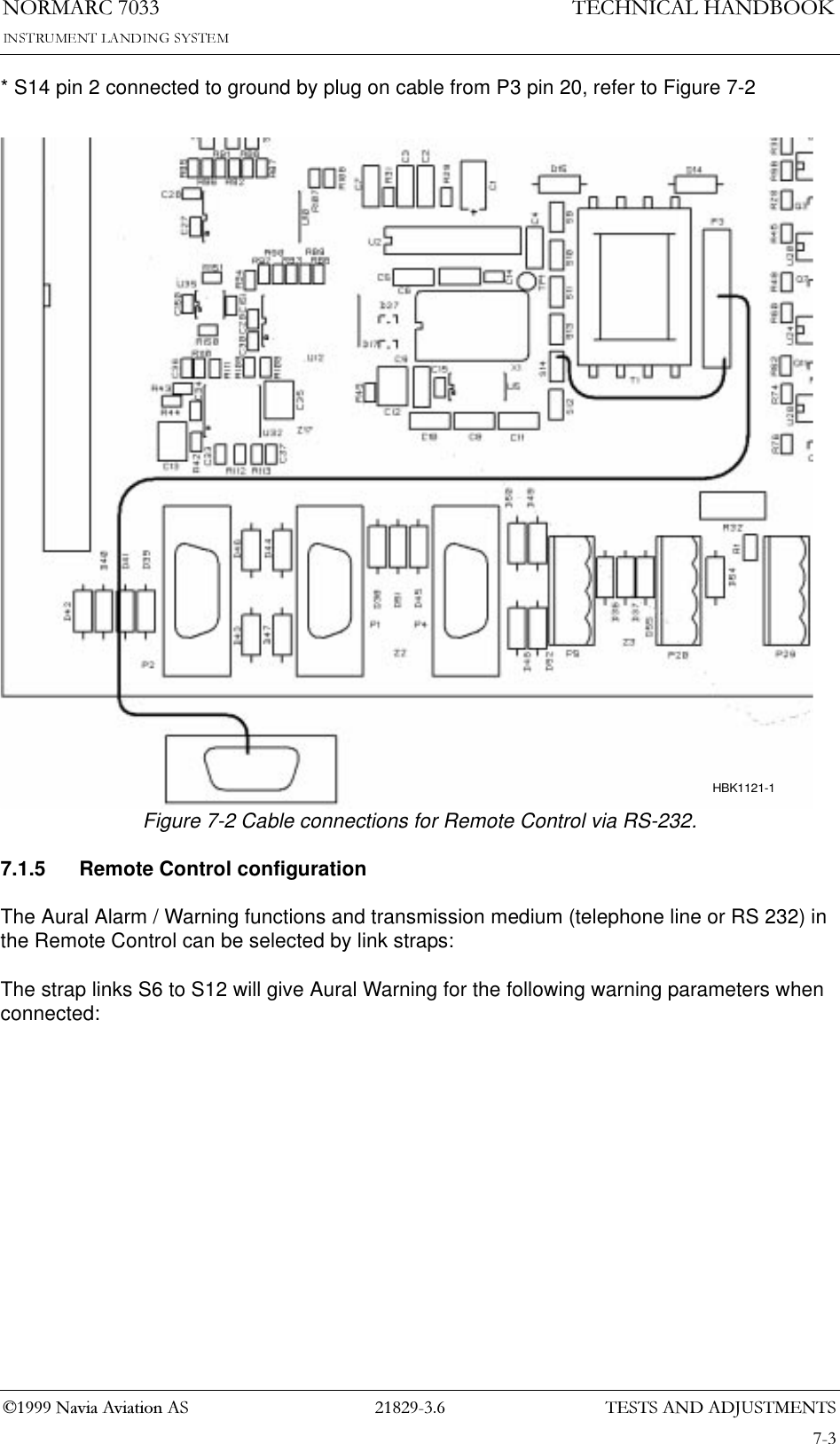
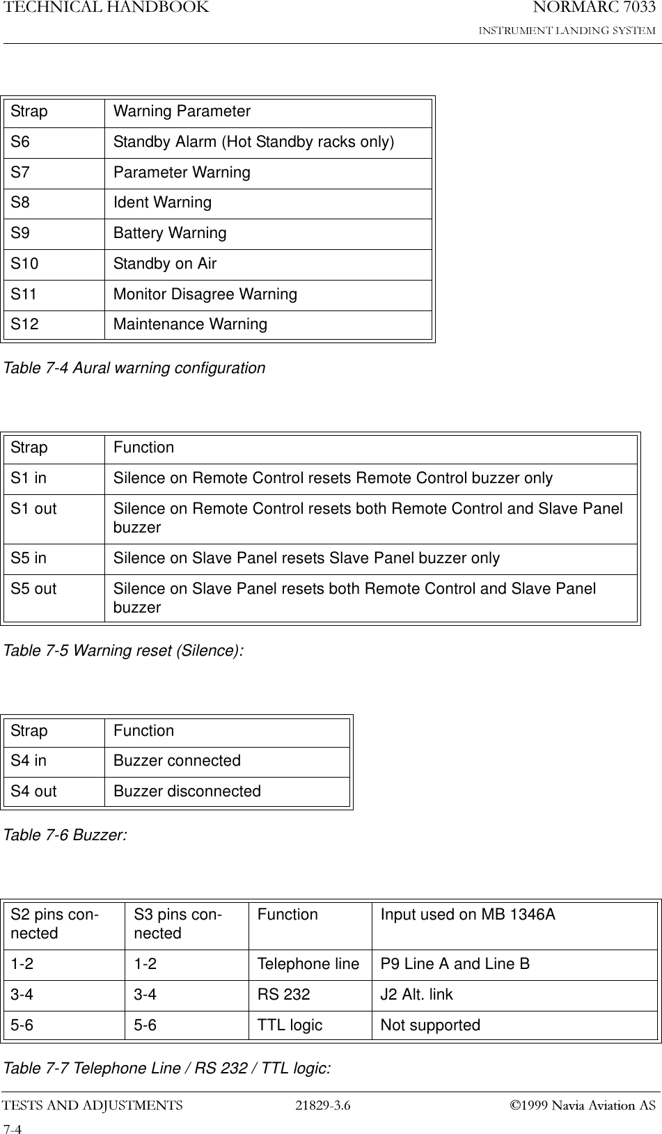
7(676$1'$'-8670(1761250$5&1DYLD$YLDWLRQ$67(&+1,&$/+$1'%22.* S14 pin 2 connected to ground by plug on cable from P3 pin 20, refer to Figure 7-2Figure 7-2 Cable connections for Remote Control via RS-232.7.1.5 Remote Control configurationThe Aural Alarm / Warning functions and transmission medium (telephone line or RS 232) in the Remote Control can be selected by link straps:The strap links S6 to S12 will give Aural Warning for the following warning parameters when connected:HBK1121-1
1250$5&7(&+1,&$/+$1'%22.7(676$1'$'-8670(176  1DYLD$YLDWLRQ$6 Table 7-4 Aural warning configurationTable 7-5 Warning reset (Silence): Table 7-6 Buzzer:Table 7-7 Telephone Line / RS 232 / TTL logic: Strap Warning ParameterS6 Standby Alarm (Hot Standby racks only)S7 Parameter WarningS8 Ident WarningS9 Battery WarningS10 Standby on AirS11 Monitor Disagree WarningS12 Maintenance WarningStrap FunctionS1 in Silence on Remote Control resets Remote Control buzzer onlyS1 out Silence on Remote Control resets both Remote Control and Slave Panel buzzerS5 in Silence on Slave Panel resets Slave Panel buzzer onlyS5 out Silence on Slave Panel resets both Remote Control and Slave Panel buzzerStrap FunctionS4 in Buzzer connected S4 out Buzzer disconnectedS2 pins con-nected S3 pins con-nected Function Input used on MB 1346A1-2 1-2 Telephone line P9 Line A and Line B3-4 3-4 RS 232 J2 Alt. link5-6 5-6 TTL logic Not supported
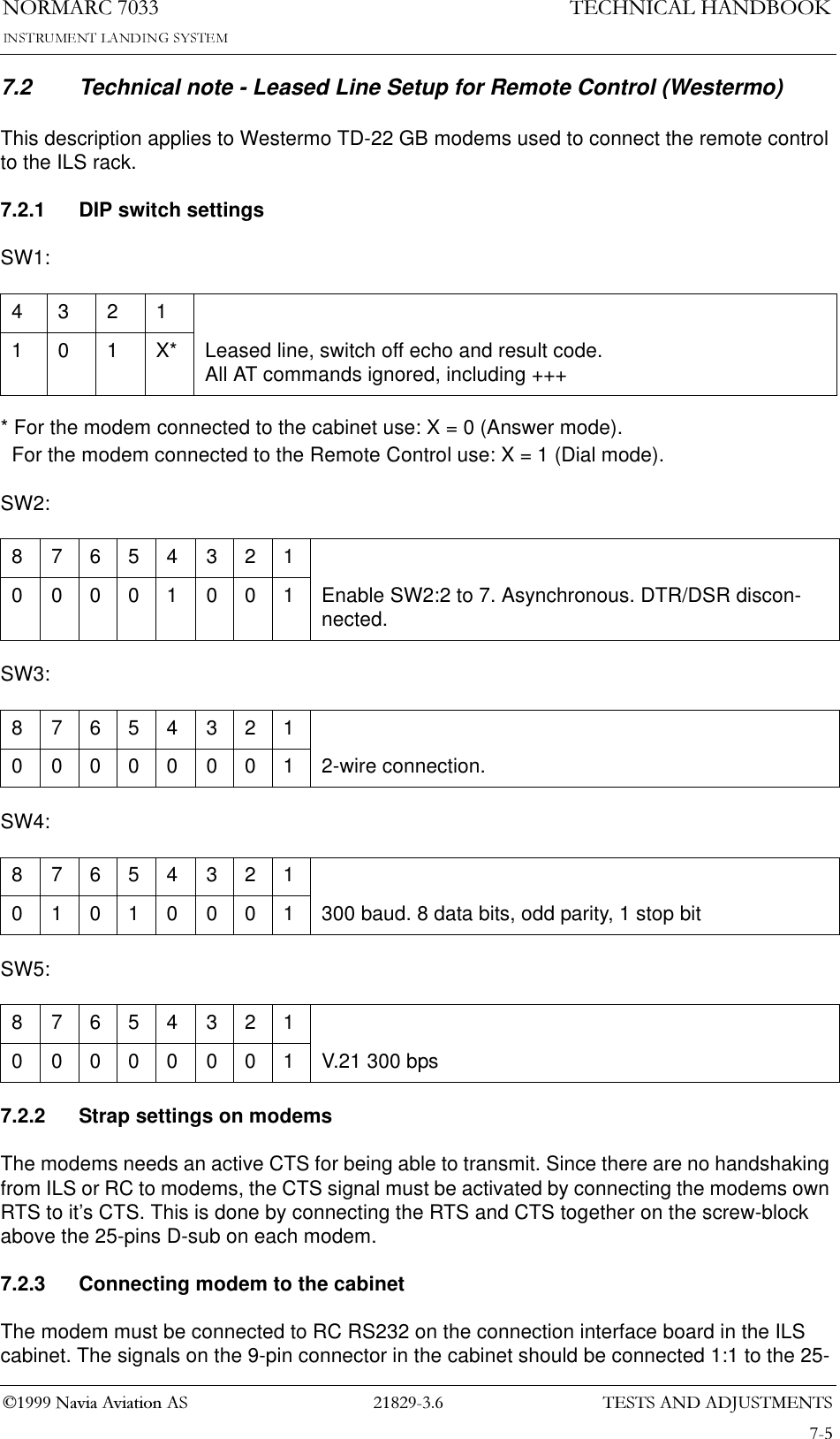
7(676$1'$'-8670(1761250$5&1DYLD$YLDWLRQ$67(&+1,&$/+$1'%22.7.2 Technical note - Leased Line Setup for Remote Control (Westermo)This description applies to Westermo TD-22 GB modems used to connect the remote control to the ILS rack.7.2.1 DIP switch settingsSW1:* For the modem connected to the cabinet use: X = 0 (Answer mode).  For the modem connected to the Remote Control use: X = 1 (Dial mode).SW2:SW3: SW4:SW5:7.2.2 Strap settings on modemsThe modems needs an active CTS for being able to transmit. Since there are no handshaking from ILS or RC to modems, the CTS signal must be activated by connecting the modems own RTS to it’s CTS. This is done by connecting the RTS and CTS together on the screw-block above the 25-pins D-sub on each modem.7.2.3 Connecting modem to the cabinetThe modem must be connected to RC RS232 on the connection interface board in the ILS cabinet. The signals on the 9-pin connector in the cabinet should be connected 1:1 to the 25-43211 0 1 X* Leased line, switch off echo and result code. All AT commands ignored, including +++8765432100001001Enable SW2:2 to 7. Asynchronous. DTR/DSR discon-nected.87654321000000012-wire connection.8765432101010001300 baud. 8 data bits, odd parity, 1 stop bit8765432100000001V.21 300 bps
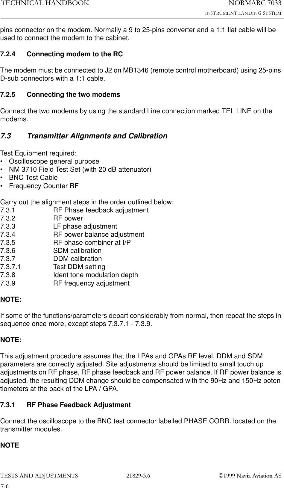
1250$5&7(&+1,&$/+$1'%22.7(676$1'$'-8670(176  1DYLD$YLDWLRQ$6pins connector on the modem. Normally a 9 to 25-pins converter and a 1:1 flat cable will be used to connect the modem to the cabinet.7.2.4 Connecting modem to the RCThe modem must be connected to J2 on MB1346 (remote control motherboard) using 25-pins D-sub connectors with a 1:1 cable.7.2.5 Connecting the two modemsConnect the two modems by using the standard Line connection marked TEL LINE on the modems.7.3 Transmitter Alignments and CalibrationTest Equipment required:• Oscilloscope general purpose• NM 3710 Field Test Set (with 20 dB attenuator)• BNC Test Cable• Frequency Counter RFCarry out the alignment steps in the order outlined below:7.3.1 RF Phase feedback adjustment7.3.2 RF power7.3.3 LF phase adjustment7.3.4 RF power balance adjustment7.3.5 RF phase combiner at I/P7.3.6 SDM calibration7.3.7 DDM calibration7.3.7.1 Test DDM setting7.3.8 Ident tone modulation depth7.3.9 RF frequency adjustmentNOTE:If some of the functions/parameters depart considerably from normal, then repeat the steps in sequence once more, except steps 7.3.7.1 - 7.3.9.NOTE:This adjustment procedure assumes that the LPAs and GPAs RF level, DDM and SDM parameters are correctly adjusted. Site adjustments should be limited to small touch up adjustments on RF phase, RF phase feedback and RF power balance. If RF power balance is adjusted, the resulting DDM change should be compensated with the 90Hz and 150Hz poten-tiometers at the back of the LPA / GPA.7.3.1 RF Phase Feedback AdjustmentConnect the oscilloscope to the BNC test connector labelled PHASE CORR. located on the transmitter modules.NOTE
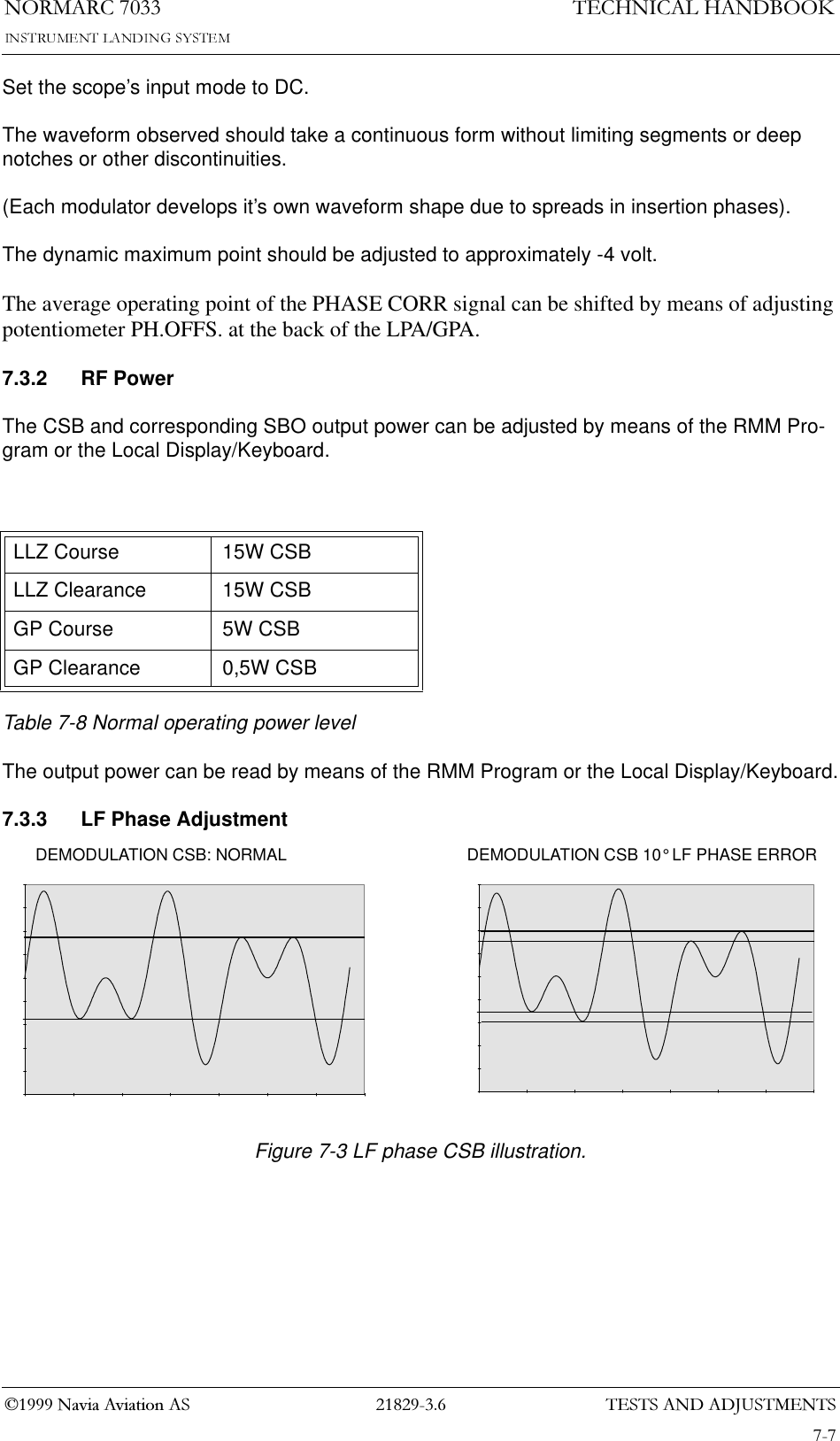
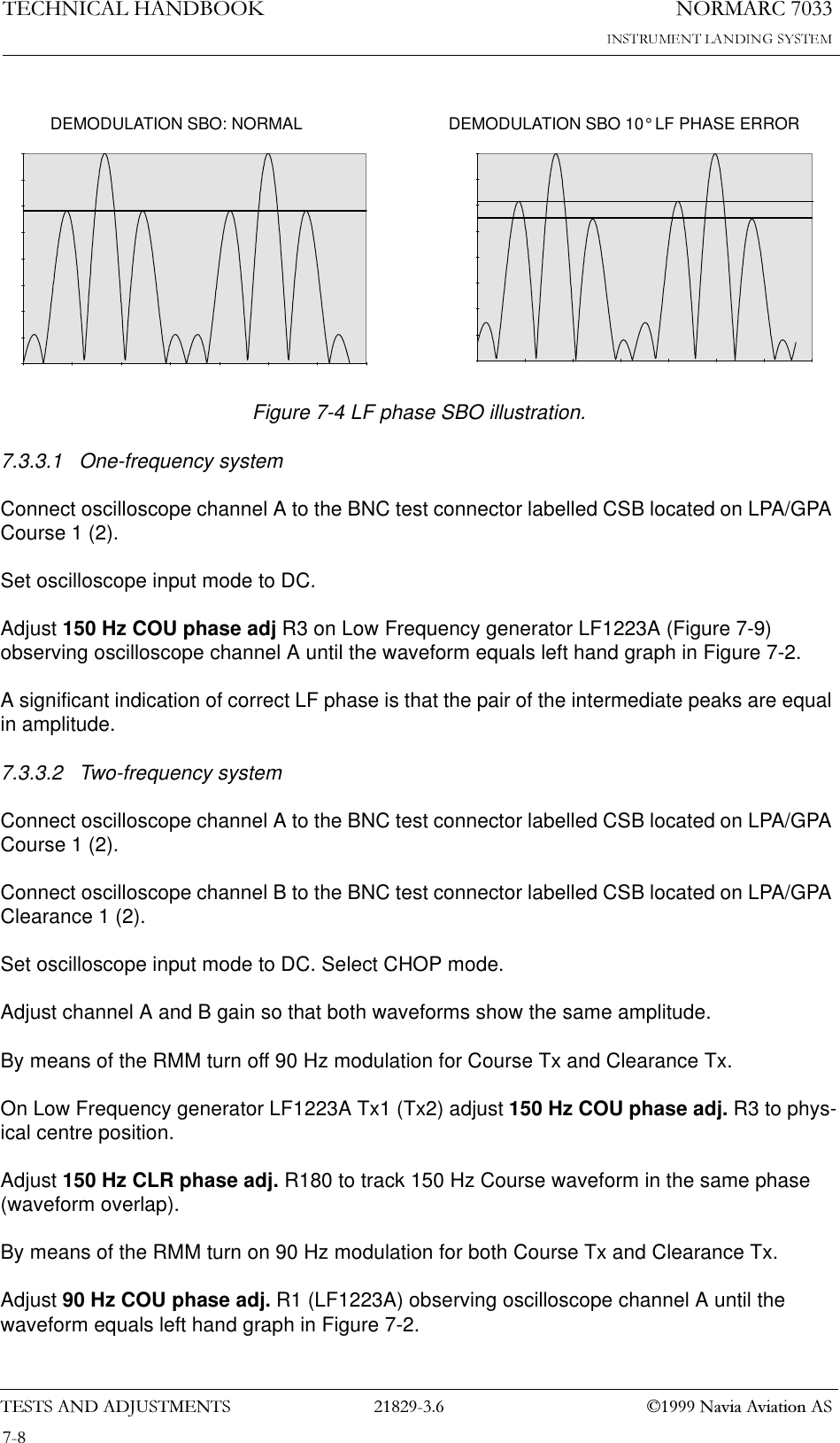
7(676$1'$'-8670(1761250$5&1DYLD$YLDWLRQ$67(&+1,&$/+$1'%22.Set the scope’s input mode to DC.The waveform observed should take a continuous form without limiting segments or deep notches or other discontinuities.(Each modulator develops it’s own waveform shape due to spreads in insertion phases).The dynamic maximum point should be adjusted to approximately -4 volt.The average operating point of the PHASE CORR signal can be shifted by means of adjusting potentiometer PH.OFFS. at the back of the LPA/GPA.7.3.2 RF PowerThe CSB and corresponding SBO output power can be adjusted by means of the RMM Pro-gram or the Local Display/Keyboard.Table 7-8 Normal operating power levelThe output power can be read by means of the RMM Program or the Local Display/Keyboard.7.3.3 LF Phase AdjustmentFigure 7-3 LF phase CSB illustration.LLZ Course 15W CSBLLZ Clearance 15W CSBGP Course 5W CSBGP Clearance 0,5W CSBDEMODULATION CSB: NORMAL DEMODULATION CSB 10° LF PHASE ERROR
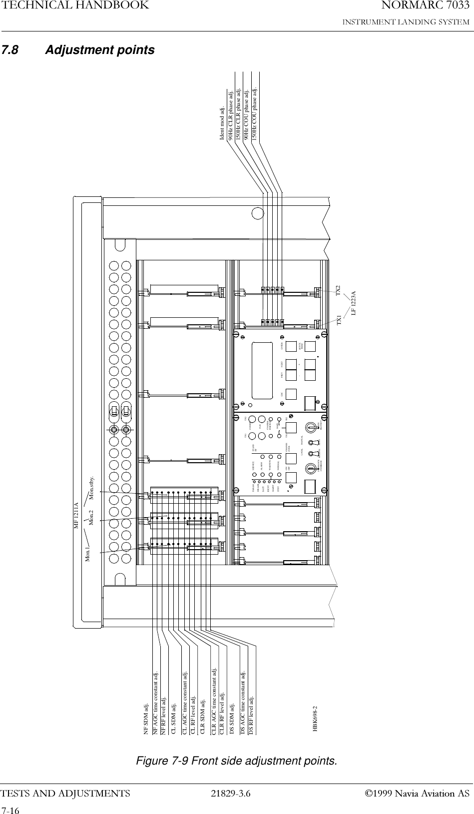
1250$5&7(&+1,&$/+$1'%22.7(676$1'$'-8670(176  1DYLD$YLDWLRQ$6Figure 7-4 LF phase SBO illustration.7.3.3.1 One-frequency systemConnect oscilloscope channel A to the BNC test connector labelled CSB located on LPA/GPA Course 1 (2).Set oscilloscope input mode to DC.Adjust 150 Hz COU phase adj R3 on Low Frequency generator LF1223A (Figure 7-9) observing oscilloscope channel A until the waveform equals left hand graph in Figure 7-2.A significant indication of correct LF phase is that the pair of the intermediate peaks are equal in amplitude.7.3.3.2 Two-frequency systemConnect oscilloscope channel A to the BNC test connector labelled CSB located on LPA/GPA Course 1 (2).Connect oscilloscope channel B to the BNC test connector labelled CSB located on LPA/GPA Clearance 1 (2).Set oscilloscope input mode to DC. Select CHOP mode.Adjust channel A and B gain so that both waveforms show the same amplitude.By means of the RMM turn off 90 Hz modulation for Course Tx and Clearance Tx.On Low Frequency generator LF1223A Tx1 (Tx2) adjust 150 Hz COU phase adj. R3 to phys-ical centre position.Adjust 150 Hz CLR phase adj. R180 to track 150 Hz Course waveform in the same phase (waveform overlap).By means of the RMM turn on 90 Hz modulation for both Course Tx and Clearance Tx.Adjust 90 Hz COU phase adj. R1 (LF1223A) observing oscilloscope channel A until the waveform equals left hand graph in Figure 7-2.DEMODULATION SBO: NORMAL DEMODULATION SBO 10° LF PHASE ERROR
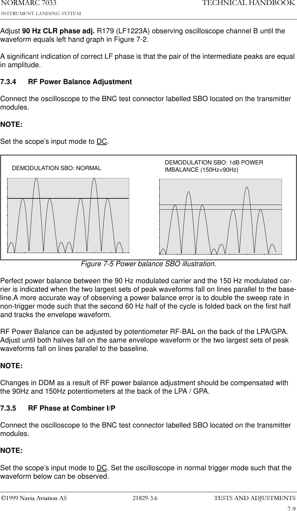
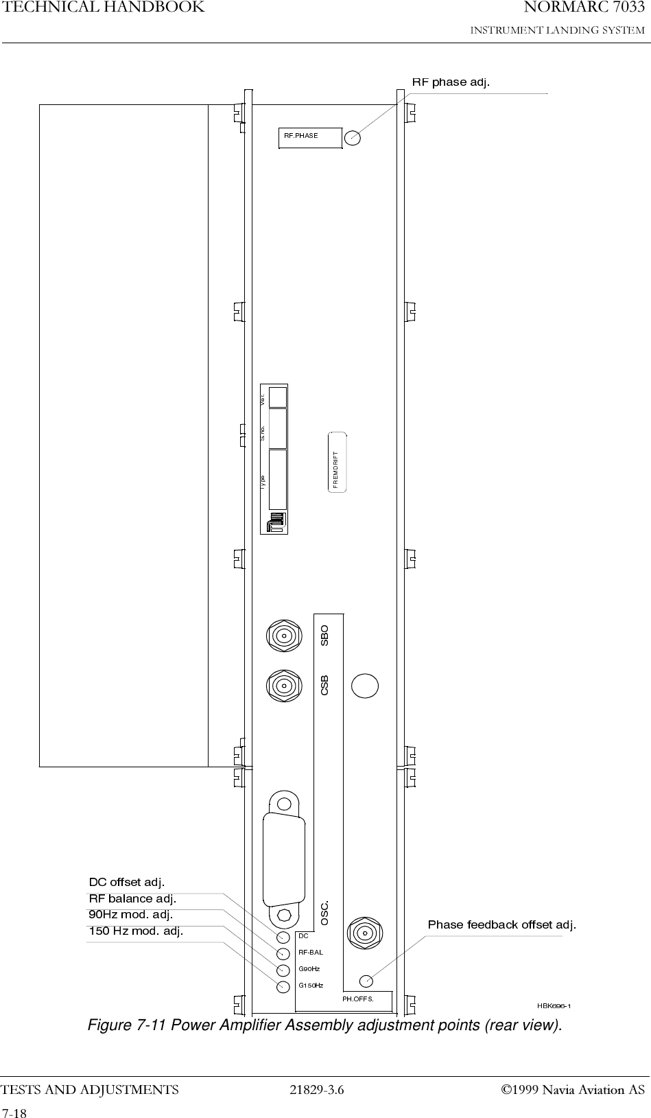
7(676$1'$'-8670(1761250$5&1DYLD$YLDWLRQ$67(&+1,&$/+$1'%22.Adjust 90 Hz CLR phase adj. R179 (LF1223A) observing oscilloscope channel B until the waveform equals left hand graph in Figure 7-2.A significant indication of correct LF phase is that the pair of the intermediate peaks are equal in amplitude.7.3.4 RF Power Balance AdjustmentConnect the oscilloscope to the BNC test connector labelled SBO located on the transmitter modules.NOTE:Set the scope’s input mode to DC.Figure 7-5 Power balance SBO illustration.Perfect power balance between the 90 Hz modulated carrier and the 150 Hz modulated car-rier is indicated when the two largest sets of peak waveforms fall on lines parallel to the base-line.A more accurate way of observing a power balance error is to double the sweep rate in non-trigger mode such that the second 60 Hz half of the cycle is folded back on the first half and tracks the envelope waveform.RF Power Balance can be adjusted by potentiometer RF-BAL on the back of the LPA/GPA. Adjust until both halves fall on the same envelope waveform or the two largest sets of peak waveforms fall on lines parallel to the baseline.NOTE:Changes in DDM as a result of RF power balance adjustment should be compensated with the 90Hz and 150Hz potentiometers at the back of the LPA / GPA.7.3.5 RF Phase at Combiner I/PConnect the oscilloscope to the BNC test connector labelled SBO located on the transmitter modules.NOTE:Set the scope’s input mode to DC. Set the oscilloscope in normal trigger mode such that the waveform below can be observed.DEMODULATION SBO: 1dB POWER IMBALANCE (150Hz<90Hz)DEMODULATION SBO: NORMAL
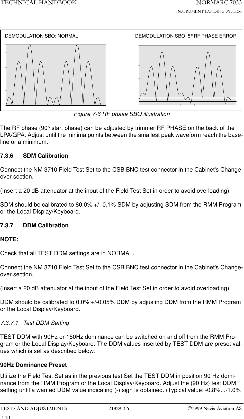
1250$5&7(&+1,&$/+$1'%22.7(676$1'$'-8670(176  1DYLD$YLDWLRQ$6.Figure 7-6 RF phase SBO illustrationThe RF phase (90° start phase) can be adjusted by trimmer RF PHASE on the back of the LPA/GPA. Adjust until the minima points between the smallest peak waveform reach the base-line or a minimum.7.3.6 SDM CalibrationConnect the NM 3710 Field Test Set to the CSB BNC test connector in the Cabinet's Change-over section.(Insert a 20 dB attenuator at the input of the Field Test Set in order to avoid overloading).SDM should be calibrated to 80,0% +/- 0,1% SDM by adjusting SDM from the RMM Program or the Local Display/Keyboard.7.3.7 DDM CalibrationNOTE:Check that all TEST DDM settings are in NORMAL. Connect the NM 3710 Field Test Set to the CSB BNC test connector in the Cabinet's Change-over section.(Insert a 20 dB attenuator at the input of the Field Test Set in order to avoid overloading).DDM should be calibrated to 0.0% +/-0.05% DDM by adjusting DDM from the RMM Program or the Local Display/Keyboard.7.3.7.1 Test DDM SettingTEST DDM with 90Hz or 150Hz dominance can be switched on and off from the RMM Pro-gram or the Local Display/Keyboard. The DDM values inserted by TEST DDM are preset val-ues which is set as described below.90Hz Dominance PresetUtilize the Field Test Set as in the previous test.Set the TEST DDM in position 90 Hz domi-nance from the RMM Program or the Local Display/Keyboard. Adjust the (90 Hz) test DDM setting until a wanted DDM value indicating (-) sign is obtained. (Typical value: -0.8%...-1.0% DEMODULATION SBO: 5° RF PHASE ERRORDEMODULATION SBO: NORMAL
7(676$1'$'-8670(1761250$5&1DYLD$YLDWLRQ$67(&+1,&$/+$1'%22.DDM).150Hz Dominance PresetUtilize the Field Test Set as in the previous test.Set the TEST DDM in position 150 Hz domi-nance from the RMM Program or the Local Display/Keyboard. Adjust the (150 Hz) test DDM setting until a wanted DDM value indicating (+) sign is obtained. (Typical value: 0.8%...1.0% DDM).Set the TEST DDM back to normal.7.3.8 Ident Tone Modulation Depth7.3.8.1 Method 1Connect the Field Test Set to the CSB BNC test connector in the Cabinet’s Change-over sec-tion.(Insert a 20 dB attenuator at the input of the Field Test Set in order to avoid overloading).Set the Ident Control to CONTINUOUS from the RMM Program or the Local Display/Key-board.On the Field Test Set, press IDENT.1020 Hz modulation depth can be adjusted from the RMM Program or the Local Display/Key-board.Adjust modulation depth to 10.0% +/-0.3%.If VOICE modulation is implemented, the ident modulation depth should be set to 5.5% +/-0.3% to avoid over modulation. Before this adjustment is done, follow the instructions in the appendix VOICE GENERATOR. Make sure VOICE is turned off from the RMM program or the Local Keyboard/Display when adjusting the modulation depth.7.3.8.2 Method 2An alternative method of checking 1020 Hz modulation depth to 10% is described below: Connect the oscilloscope to the BNC test Connector labelled CSB.Switch off the 90 Hz modulation and the 1020 Hz modulation.Note the peak-to-peak deflection of the remaining 150 Hz waveform.Then switch off the 150 Hz modulation and switch the 1020 Hz modulation to CONTINUOUS.The observed 1020 Hz peak-to-peak waveform amplitude should be 50% of the 150 Hz ampli-tude providing the 1020 Hz modulation depth is 10% (or 1/2 of 150 Hz depth).7.3.9 RF Frequency AdjustmentFine-adjustment of the operating frequency can be carried out by adjusting C1 in the OS1221A/B RF Oscillator module.
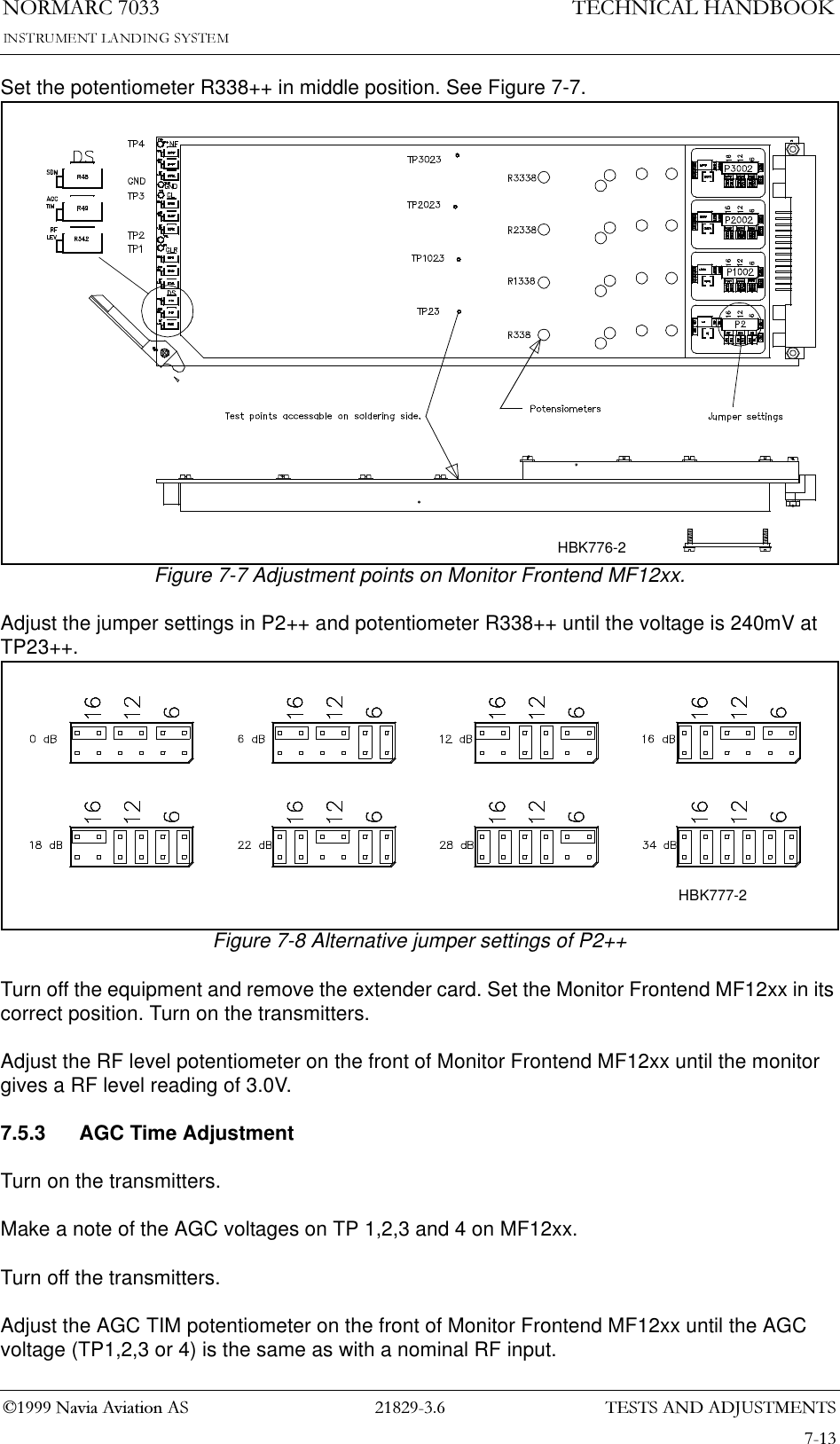
1250$5&7(&+1,&$/+$1'%22.7(676$1'$'-8670(176  1DYLD$YLDWLRQ$6The top cover must be removed.Mount the Oscillator OS1221A/B on an extension board.In order to monitor the frequency, connect the Frequency Counter to the BNC test connector labelled CSB. (Make sure the transmitter under test is routed to Antenna). If necessary for sta-ble counting switch off modulation tones. Adjust until frequency is less than 1 kHz from operating frequency. Trimmer C1 adjusts course and clearance frequencies simultaneously.7.4 Antenna System AdjustmentsAfter the transmitters has been aligned correctly the antenna system must be aligned. This includes mechanical adjustments of the Antenna System, electrical adjustments (phasing) and adjustments of the ADU and MCU.For details, refer to the adjustment procedure for each antenna system.7.5 Monitor Alignment and Calibration.Test Equipment required:• Oscilloscope, general purpose• NM 3710 Field Test Set (with 20 dB attenuator)• BNC Test Cable• Digital Voltmeter, 4 digits, DC7.5.1 GeneralDescription is given only for the DS channels. R338++ means that the other channels has numbers R1338, R2338 and R3338 for CL, CLR and NF channels.Before any monitor adjustments are attempted, the following procedures shall be completed: Transmitter calibrationsNetwork alignmentsIt is imperative for the result that the signals from the Monitor Combining Network (MCU) are correct. Check these signals with the NM3710, Field Test Set,These signals are used for aligning the monitors. 7.5.2 RF Input Level Adjustment.Mount the Monitor Frontend MF12xx on an extender card.Turn on the transmitters.
7(676$1'$'-8670(1761250$5&1DYLD$YLDWLRQ$67(&+1,&$/+$1'%22.Set the potentiometer R338++ in middle position. See Figure 7-7.Figure 7-7 Adjustment points on Monitor Frontend MF12xx.Adjust the jumper settings in P2++ and potentiometer R338++ until the voltage is 240mV at TP23++. Figure 7-8 Alternative jumper settings of P2++Turn off the equipment and remove the extender card. Set the Monitor Frontend MF12xx in its correct position. Turn on the transmitters.Adjust the RF level potentiometer on the front of Monitor Frontend MF12xx until the monitor gives a RF level reading of 3.0V.7.5.3 AGC Time AdjustmentTurn on the transmitters.Make a note of the AGC voltages on TP 1,2,3 and 4 on MF12xx.Turn off the transmitters.Adjust the AGC TIM potentiometer on the front of Monitor Frontend MF12xx until the AGC voltage (TP1,2,3 or 4) is the same as with a nominal RF input.HBK776-2HBK777-2
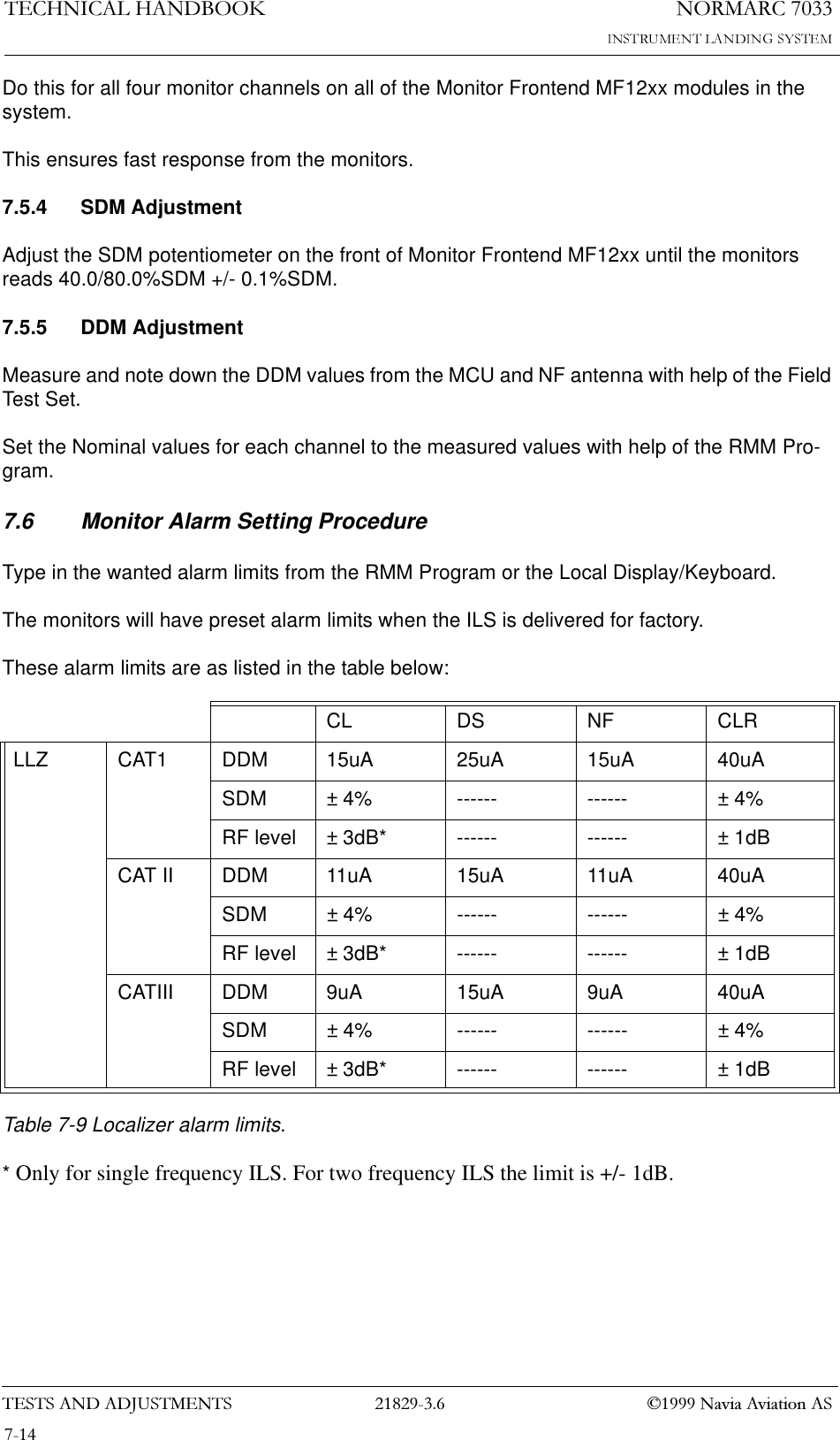
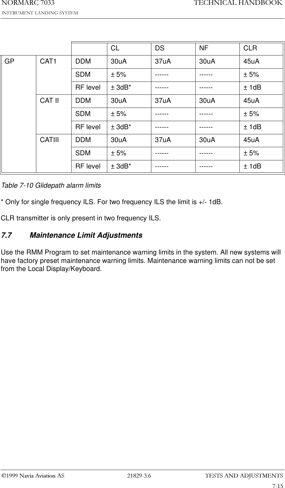
1250$5&7(&+1,&$/+$1'%22.7(676$1'$'-8670(176  1DYLD$YLDWLRQ$6Do this for all four monitor channels on all of the Monitor Frontend MF12xx modules in the system.This ensures fast response from the monitors.7.5.4 SDM AdjustmentAdjust the SDM potentiometer on the front of Monitor Frontend MF12xx until the monitors reads 40.0/80.0%SDM +/- 0.1%SDM.7.5.5 DDM AdjustmentMeasure and note down the DDM values from the MCU and NF antenna with help of the Field Test Set.Set the Nominal values for each channel to the measured values with help of the RMM Pro-gram.7.6 Monitor Alarm Setting ProcedureType in the wanted alarm limits from the RMM Program or the Local Display/Keyboard.The monitors will have preset alarm limits when the ILS is delivered for factory.These alarm limits are as listed in the table below:Table 7-9 Localizer alarm limits. * Only for single frequency ILS. For two frequency ILS the limit is +/- 1dB.CL DS NF CLRLLZ CAT1 DDM 15uA 25uA 15uA 40uASDM ± 4% ------ ------ ± 4%RF level ± 3dB* ------ ------ ± 1dBCAT II DDM 11uA 15uA 11uA 40uASDM ± 4% ------ ------ ± 4%RF level ± 3dB* ------ ------ ± 1dBCATIII DDM 9uA 15uA 9uA 40uASDM ± 4% ------ ------ ± 4%RF level ± 3dB* ------ ------ ± 1dB
7(676$1'$'-8670(1761250$5&1DYLD$YLDWLRQ$67(&+1,&$/+$1'%22.Table 7-10 Glidepath alarm limits* Only for single frequency ILS. For two frequency ILS the limit is +/- 1dB.CLR transmitter is only present in two frequency ILS.7.7  Maintenance Limit AdjustmentsUse the RMM Program to set maintenance warning limits in the system. All new systems will have factory preset maintenance warning limits. Maintenance warning limits can not be set from the Local Display/Keyboard.CL DS NF CLRGP CAT1 DDM 30uA 37uA 30uA 45uASDM ± 5% ------ ------ ± 5%RF level ± 3dB* ------ ------ ± 1dBCAT II DDM 30uA 37uA 30uA 45uASDM ± 5% ------ ------ ± 5%RF level ± 3dB* ------ ------ ± 1dBCATIII DDM 30uA 37uA 30uA 45uASDM ± 5% ------ ------ ± 5%RF level ± 3dB* ------ ------ ± 1dB
1250$5&7(&+1,&$/+$1'%22.7(676$1'$'-8670(176  1DYLD$YLDWLRQ$67.8 Adjustment pointsFigure 7-9 Front side adjustment points.11LF 1223AMF 1211AESC PREV NEXT-+ENTERREADQUICKCLRCOAXIALCOURSEMAINPOSITIONWRITEPROTECTWARNINGON/NORMALINTERLOCKOVERRIDEMAINTSTBYOFFREMOTELOCALAUTOMANUALOVERCHANGE TX1ALARMSERVICEPARAMDISAGRBATTIDENTTX1TX2TX2STANDBYMon.1 Mon.2 Mon.stby.90Hz COU phase adj.150Hz COU phase adj.90Hz CLR phase adj.150Hz CLR phase adj.TX1 TX2NF SDM adj.NF AGC time constant adj.NF RF level adj.CL SDM adj.CL AGC time constant adj.CL RF level adj.CLR SDM adj.CLR AGC time constant adj.CLR RF level adj.DS SDM adj.DS AGC time constant adj.DS RF level adj.Ident mod adj.HBK698-2
7(676$1'$'-8670(1761250$5&1DYLD$YLDWLRQ$67(&+1,&$/+$1'%22.Figure 7-10 CI1210A Connection Interface adjustment point.TEMPINDOOR TEMPOUTDOOR ACLEVEL ANALOGCH.1 ANALOGCH.2 ANALOGCH.3 DIGITALPORT A DIGITALPORT B DIGITALPORT C DIGITALPORT DTO MB1203RS232 RS232 RS232 REMOTECONTROLDC-LOOP DC-LOOP DMELOCAL REMOTE 2 REMOTE 1 CH.1&2 CH.3&4BATTERYWARNINGBattery protection level adj.HBK697-1
1250$5&7(&+1,&$/+$1'%22.7(676$1'$'-8670(176  1DYLD$YLDWLRQ$6Figure 7-11 Power Amplifier Assembly adjustment points (rear view).
)81&7,21$/'(6&5,37,211250$5&1DYLD$YLDWLRQ$67(&+1,&$/+$1'%22.3$57,,,'(6&5,37,218 Functional Description8.1 IntroductionThe NM 7000-series Instrument Landing System is a fourth generation system featuring extensive remote maintenance and monitoring features and systematic use of modern elec-tronic components and processors.Careful analysis has guided the partitioning of the system into analog hardware, digital hard-ware and software to meet the reliability and integrity objectives as well as easy maintenance and low cost of ownership.In the monitor, comparison between monitor measurements and stored monitor limits is per-formed by digital hardware. Thus safety critical software is avoided in those functions. The fil-tering functions are performed by a dedicated signal processor running a FFT algorithm, with the signals sampled after base-band detection.The transmitter/modulator uses a synthesizer as a RF source. In two-frequency systems a common reference crystal is used, avoiding drift in difference frequency. The LF and ident fre-quencies and ident keying are generated by digital hardware, while the level setting and mod-ulation control are performed by digitally controlled analog feedback loops.Local and remote control, and change-over and shut-down functions are performed by digital hardware.Software is used for the remote maintenance and monitoring functions, including alarm and parameter storage, diagnostic functions, transmitter adjustments and change of monitor limits. Appropriate hardware protection is used to avoid that the software becomes safety critical.TechnologyMost of the modules in the NM 7000-series ILS are based on surface mount components on multi-layer boards. This reduces the number of modules, and gives very good EMC/EMI per-formance. Most of the digital hardware is contained in field programmable gate arrays (FPGA), giving very high reliability. The processors used are well proven Texas and Intel types. In the RF stages, modern RF power FET transistors are used.
1250$5&7(&+1,&$/+$1'%22.)81&7,21$/'(6&5,37,21  1DYLD$YLDWLRQ$6.Figure 8-1 ILS Block DiagramEach block is described separately in the following sections.8.2 TransmitterThe transmitter section generates the ILS signal with the required RF power levels and modu-lations levels. The section comprises two identical transmitters, TX 1 and TX 2, where one is connected to the antenna, while the other is connected to dummy loads, acting as a back-up.The reference signals in the transmitter section are RF signals from the oscillator OS1221AB and LF modulation signals (90Hz and 150Hz) from the low frequency generator LF1223A. System DC voltages comes from the Power Supply board PS1227A.In each transmitter, the RF oscillator has separate outputs for Course and Clearance. These two channels are offset by 10 kHz. The LF Generator also has independent outputs for Course and Clearance.The GPA 1231A Glidepath Course Power Amplifier Assembly contains modules to modulate, amplify and combine signals into the required CSB and SBO signals. Amplitude- and RF phase feedback ensures correct RF power level and modulation.The Clearance transmitters GPA1232A generate only CSB signals, and only amplitude feed-back is therefore incorporated.The COA 1207A/C Change Over section has relays to connect the CSB and SBO outputs from one transmitter to the antenna while the other is connected to dummy loads. The relays are controlled by a Coax-control signal. SBO phase shifters and attenuators are incorporated for obtaining the correct CSB/SBO relationship. The block diagram is shown on the next page. MonitorFrontendMF1211/MF1219MonitorMO1212RMSRMA1215MonitorMO1212TX controlTCA1218RF oscillatorOS1221ChangeoverSectionConnectionInterface CI1210MonitorinputsignalsMonitorinputsignals LF oscillatorLF1223TransmitterLPA/GPARF oscillatorOS1221LF oscillatorLF1223 TransmitterLPA/GPANAVsignalsoutRemoteControlExternalsensorsComm.portsData anddiagnosticsMonitorFrontendMF1211/MF1219Monitor 1Monitor 2Transmitter 1Transmitter 2HBK549-1
)81&7,21$/'(6&5,37,211250$5&1DYLD$YLDWLRQ$67(&+1,&$/+$1'%22.    Figure 8-2 System Block Diagram of a 2-Frequency GP TransmitterPHASER ATTENUATORPHASER ATTENUATORCOAXRELAYCOAXRELAYCSBCSBSBOSBOOUTPUTSBO COURSEOUTPUTCSB COURSEMONITORCSBCOUPLERCOAX CONTROLCOAX CONTROLCOAXRELAYOUTPUTCSB CLEARANCEMONITORCSBCOUPLERCOAX CONTROLRF OSC.TX2RF OSC.TX1LF GEN.TX1LF GEN.TX2CHANGEOVER COUCHANGEOVER CLRCSBCSB POWER AMPLIFIER ASSEMBLY  COU-TX2 POWER AMPLIFIER ASSEMBLY  COU-TX1 POWER AMPLIFIER ASSEMBLY  CLR-TX1 POWER AMPLIFIER ASSEMBLY  CLR-TX2AMPLITUDE  FEEDBACKAM-MOD. HPAFEEDBACKCONTROLAMPLITUDE  FEEDBACKAM-MOD. HPAFEEDBACKCONTROLAMPLITUDE & RF PHASE FEEDBACKAM-MOD. HPAHPAHYBRIDFEEDBACKCONTROLAM-MOD.AMPLITUDE & RF PHASE FEEDBACK50 ohm50 ohm50 ohmAMPLITUDE & RF PHASE FEEDBACKAM-MOD. HPAHPAHYBRIDFEEDBACKCONTROLAM-MOD.AMPLITUDE & RF PHASE FEEDBACKHBK 591-1
1250$5&7(&+1,&$/+$1'%22.)81&7,21$/'(6&5,37,21  1DYLD$YLDWLRQ$68.3 MonitorThe monitor section’s main task is to generate alarms if the transmitters fail. The alarm signals are interpreted by the station control section which decides whether to change transmitter or to shut the ILS signals down. Warning information is treated by the RMS.The input signals to the monitor are RF signals, CL, DS, NF, CLR(2 freq. only), from the antenna system. In addition the DC loop detects failures in the antenna and an optional exter-nal frontend may monitor alarm generating parameters from additional equipment (i.e. a far field monitor). The outputs are alarm status to the transmitter control section, parameter val-ues to the RMS and DC loop reference voltages to the antenna system.The monitor chain consists of the Monitor Frontend module, MF1211A in LLZ and MF1219A in GP, and the Monitor module MO1212A. This chain is duplicated to increase reliability. In hot standby configurations an additional chain monitors the standby transmitter. See the figure below.The Monitor Frontend module is mainly an AM receiver which detects the baseband signals and generates DC voltages proportional to the RF level. In addition a digital pulse train is gen-erated, to tell the difference in frequency (DF) between the COU and CLR transmitters in two frequency configurations.The Monitor module digitizes the analog signals, filters all data by FFT or mean value calcu-lations, and passes the parameters to the comparator. The comparator generates alarm sig-nals if the parameters are outside the programmed limits.Figure 8-3 Monitor section block diagram.8.4 Transmitter ControlThe transmitter control sections main purpose is to control the transmitters on/off state. This is done based on alarm inputs from the monitors, inputs from remote control, inputs from local keyboard (front panel for station control) and inputs from the RMM system.The station control receives alarm information from the monitors. Based on the alarm status DS_RFExternal Frontend 1DC loopFIFOMUX DigitalFiltersComp. Alarm busRMS busDC loopExternal Frontend 2NAVMon.1NAV Mon.2NAV Mon.St.byAM receiverCL_RFAM receiverCLR_RFAM receiverNF_RFAM receiverMixerFIFOLimitStorageMONITOR FRONTEND 1 MONITOR 1MONITOR FRONTEND 2STANDBY MONITOR FRONTENDMONITOR 2STANDBY MONITORDS_RF_LEVELDS_BASEBANDCL_RF_LEVELCL_BASEBANDDFCLR_RF_LEVELCLR_BASEBANDNF_RF_LEVELNF_BASEBAND(SC/TRM)HBK556-1
)81&7,21$/'(6&5,37,211250$5&1DYLD$YLDWLRQ$67(&+1,&$/+$1'%22.and the current mode of operation, the station control decides if a changeover/shutdown should occur. The station control unit also receives user/state inputs from remote control (example: Interlock) and the RMM system (example: Warning lamp outputs). Configuration selections on the TC1216A board also affects the operation of the station control.Figure 8-4 TCA1218A/B Block DiagramThe transmitter control assembly, TCA1218A/B consists of the transmitter control (TC) mod-ule TC1216A and the local control (LC) front panel LC1217A/B (the B-version is a front panel designed for hot standby configuration). See Figure 8-4.The main functions of the TCA1218A/B are performed by the station control (SC) part of the transmitter control (TC). The SC takes care of the normal operating tasks like turning transmit-ters on/off bases on various inputs that may affect the transmitter status. The SC also has a RMS interface enabling the RMM system to read the status of the SC and to illuminate warn-ing lamps etc. The terminator (TRM) part of the TC takes over and shuts the ILS down if the SC is not able to operate as expected. The TRM shut down the power to the transmitters approximately 1 sec-TX CONTROLTERMINATORSHUTDOWNUNITALARMRC busREMOTECONTROLINTERFACETERMINATORSTATION CONTROLCONTROLANDUARTALARMDETECTIONANDVOTINGALARMSTANDBYALARMALARMDETECTIONANDVOTINGTerminator alarmLOCAL busRMS busTerminatoralarm busTX control busRC i/f busTC1216ALC1217A/BStation control alarm busLocal Controlswith/withouthot standby LEDsTransmitter ControlHBK543-1
1250$5&7(&+1,&$/+$1'%22.)81&7,21$/'(6&5,37,21  1DYLD$YLDWLRQ$6ond after an alarm situation or interlock state has occurred.The remote control interface process serial data from/to the remote control. This unit also detects and reports faults in data transmission with remote control. The data from the remote control are sent to both SC and TRM.The local control displays the transmitter status of the ILS. It also provides a user interface, enabling the user to perform basic operations on the ILS.8.5 Remote control systemThe remote control’s main purpose is to provide an interface to the ILS from the control tower, or technical equipment room at the airport.The remote control provides the ILS with user inputs and selections. The unit also displays the status of the ILS using LEDs.The remote control system consists of an UART/line interface, RC1241A, a front panel, RF1242A/B (B is a front panel for hot standby configuration) and a slave panel.The remote control assembly, RCA1240A/B, consists of the remote control (RC) module RC1241A and the remote control front panel (RF) RF1242A/B (the B-version is a front panel designed for hot standby configuration). See Figure 8-5.Figure 8-5 RCA1240A/B Block DiagramThe line interface in RC1241A convert signals between standard serial data format and tele-phone line signals both ways using a FSK modem (compatible with CCITT V.21).The UART /control in RC1241A performs serial/parallel conversion. Pushbutton, switch and operational mode (interlock) status is sent from remote control to ILS. Transmitter status and other info is received from the ILS.The front panel RF1242A/B contains the pushbuttons, switches and LEDs for the user.The slave panel is an optional control panel with a limited set of functions/LEDs, designed for use in the airport tower.LINEINTERFACERF1242A/BTelephoneline CONTROLANDUARTSlave busRemote Control front panelwith/without hot standbylamp indicationsRC1241ASlave panel(s)HBK544-1
)81&7,21$/'(6&5,37,211250$5&1DYLD$YLDWLRQ$67(&+1,&$/+$1'%22.8.6 Remote Monitoring System (RMS)8.6.1 General DescriptionThe Remote Monitoring System consists of a CPU-board located inside the main cabinet, with several means of collecting data from both inside and outside the equipment. The RMS also constitutes the operator interface, offering up to three RS232 interfaces, and the Local Key-board/Display. The main tasks are:• Collection of executive monitor parameters and maintenance parameters• Generation of system warnings• Maintaining historical storages of all data.• ‘Snap-shot’ of all monitor and maintenance data immediately before alarm occurrence.• Setting of alarm limits and tx parameters.• Fault isolation.• Controlling the Local Keyboard/Display.The RMS SW comprises a resident part located in the ILS. It communicates with the RMM PC program via dedicated lines or a MODEM. The PC SW is the main operator interface with the ILS.Data collection is facilitated in 3 different ways: A parallel high speed data bus offering both read and write operations, a IIC-standard serial bus, and a set of 24 different ADC channels.Figure 8-6 The RMM configuration.8.6.2  PC and ModemThe main operator interface is locally or remotely connected personal computers, running dedicated SW and communicating with the main cabinet resident SW via a dedicated proto-col. The system facilitates three channels for PC connections, two of which can be used for remote PC via modems and leased-line or dial-up telephone lines. All three PC’s can be logged on simultaneously, but only one of them can have write access at a given point in time.RMA 1215ARemotePC 2RemotePC 1LocalPCRS232RS232RS232 RS232RS232RS232Dial-uporleased-lineIICserial busAnalogchannelsRMSdata busCI 1210ALocalRemote 1Remote 2Serial InterfaceInterface CircuitryLCD / KeyboardCPUMAIN CABINETMODEMMODEMMODEMMODEMDigitalandAnalogInputsAnalogInputsMonitorDataandSystemSettingsHBK569-1
1250$5&7(&+1,&$/+$1'%22.)81&7,21$/'(6&5,37,21  1DYLD$YLDWLRQ$68.6.3 RMS DatabusThe main operation of the RMS parallel data bus is continuously to collect data from the Mon-itor MO 1212A. Additional functions are setting of monitor alarm limits and delays on the MO 1212A, setting of TX-parameters on LF-generator LF1223A, and reading of system status from the TX Control Assembly TCA 1218A/B. Writing of warning status to the TCA 1218A/B is also done via the RMS databus.Figure 8-7 The RMS databus.8.6.4 Maintenance Data CollectionIn order to facilitate fault isolation and presentation, several analog and digital measuring points are distributed throughout the system. These point are primarily accessed via the IIC serial bus. In addition, 24 ADC-channels are read directly into the RMA 1215A board.The IIC serial bus collects digital status information from MF1219A, MO1212A, LF1223A, OS1221B and the CI 1210A connection interface card. 6 of these are user configurable inputs/outputs. In addition, analog measurements are obtained from the GP - Power Assem-blies GPA1231A and GPA1232A.The ADC-channels are mainly used to measure power amplifier current consumptions, as well as system voltages. These measurements are obtained from the Power Supply boards PS1227A. In addition system current consumption, as well as several user configurable inputs, are measured on the CI1210A board.RMA 1215AMO 1212AMON1MO 1212AMON2LF 1223ATX1LF1223ATX2 TCA 1218A/BRMS DatabusMO 1212ASTB MONHBK568-1
)81&7,21$/'(6&5,37,211250$5&1DYLD$YLDWLRQ$67(&+1,&$/+$1'%22.Figure 8-8 The IIC serial bus and ADC channels.8.7 Power SupplyThe ILS main cabinet is supplied from one or two 27V power supplies with a backup battery. The 27V is regulated down to ±15V, 8.5V and 5V. The transmitter power amplifiers are fed directly from the 27V supply, while the rest of the system uses the regulated voltages.Current measurements are done on the power supply, the battery and each power amplifier. Each regulated voltage is measured in the Power Supply PS1227A. The results are presented to the user through the RMS system.When the ILS signals are shut down, the power supply to the power amplifiers are actually turned off by relays. This is controlled by the terminator alarm signal from the station control section.The backup battery is protected against deep discharge with a protection circuit. This circuit disconnects the battery when the voltage drops below 22V.A battery warning is given through the RMS system when the primary power supply (supplies) fails.RMA 1215AMF 1219AMON1 MF 1219AMON2 MO 1212AMON1 MO 1212AMON2 PS 1227A #1 PS 1227A #2LF 1223ATX1 LF 1223ATX1 GPA 1231ATX1 COU GPA 1232ATX1 CLR GPA 1231ATX2 COU GPA 1232ATX2 CLRCI 1210AIIC serialbusADCchannelsMF 1219ASTB MON MO 1212ASTB MONOS 1221BTX1 OS 1221BTX2HBK571-1
1250$5&7(&+1,&$/+$1'%22.)81&7,21$/'(6&5,37,21  1DYLD$YLDWLRQ$6.Figure 8-9 Power supply functional diagram.AAACDCDCDCDCDCDCDCDCDCTerminatorAlarmDCDCDCDCDCDCDCDCMODULE CONNECTIONSTX1 TX2PA123xA CL 90HzPA123xA CL 150HzPA123xA CLR 90HzPA123xA CLR 150HzPA123xA CL 90HzPA123xA CL 150HzPA123xA CLR 90HzPA123xA CLR 150HzMF121xAMO1212ARMA1215ALF1223AOS1221xCI1210AAC1226ATCA1218AMainCabinetSwitchCI1210APS1227A-1PS1227A-2VVVVVVVV+--AAAAAAAABattery WarningV27_CL1501V27_CL901V27_CLR901V27_CLR1501V15PV15NVDDV8P5PV27_CL1502V27_CL902V27_CLR902V27_CLR1502MF121xAOS1221AxPA123xAMAIN CABINETHBK584-2
'(7$,/(''(6&5,37,211250$5&7(&+1,&$/+$1'%22.1DYLD$YLDWLRQ$69 Detailed descriptionThis chapter gives a detailed description of the assemblies and modules in the NM7033.Notations in the block diagrams:  ~ - Active low signal.[7:0] - Signal bus numbering system.  Here, an eight bits bus, numbered from seven down to zero.9.1 Main CabinetThe following paragraphs describe the electronics modules located in the main cabinet.9.1.1 MF1219A Glidepath Monitor FrontendGeneral Description:The MF1219A module demodulates the ILS RF signals from the antenna system, and passes baseband and RF level signals, and a digital pulstrain representing the difference in frequency (DF) between the CL and CLR signals, to the monitor MO1212A (chapter 9.1.2). The CLR channel and DF circuit are used in two frequency systems only.Block Diagram:See Figure 9-1.Block Description:The MF1219A module has four identical channels:• DS - Displacement Sensitivety• NF - Near Field• CL - Course Line• CLR - CLeaRenceIn addition a mixer circuit extracts the difference frequency between CL RF and CLR RF, and a maintainance monitor reports low level RF amplitude and modulation depth to the RMS.CL_FILTconsists of a step attenuator and a bandpass filter covering the bandwith 328-336 MHz. The step attenuator can be set in the range 0 to 34 dB by setting jumper plugs enabling one or more of three attenuators each providing 6dB, 12dB and 16 dB attenuation.CL_RFAMPsplits the band limited RF signal to the baseband chain and the RF level chain.  The baseband amplifier stage comprises automatic gain control (AGC) through a pin diode attenuator.CL_LEVdetects a DC voltage proportional to the RF input level, through a detector diode and a low pass filter.CL_BASEBdetects the baseband signals and generates the control voltage to the AGC stage of the CL_RFAMP.  When no RF signal is present, the AGC voltage is clamped to a preset level.
1250$5&7(&+1,&$/+$1'%22.'(7$,/(''(6&5,37,21  1DYLD$YLDWLRQ$6CL_LPFIare active lowpass filters that attenuates frequencies above the ILS baseband.DF_MIXERmixes the CL and CLR RF signals and extracts the difference frequency. The output signal is a TTL level pulse train.MAINTMONmonitors the RF levels and the modulation depths, and reports to the RMS if the levels exceed the preset limits.
'(7$,/(''(6&5,37,211250$5&7(&+1,&$/+$1'%22.1DYLD$YLDWLRQ$6.Figure 9-1 MF1219A Block diagram (CL channel shown)CL_BASEBCURRENT-CONTROLLEDATTENUATORCL_RFAMPRF LEVELVERNIERSTEPATTENUATORBANDPASSFILTERCL_FILTLOWPASS FILTERBASEBANDRF INPUTCL_LPFIDF_MIXERACTIVE MIXERFrom CLR channelDFLOWPASSFILTERPRESETAGC LEVELRF LEVELDC OUTCL_LEVRF LEVELAGCMUXPart of MAINTMONCL_IDENTIIC_SDAIIC_SCLVOLTAGEREFERENCECOMPARATORAGC_VOLTTP 1...4TPxx23AGC_TIMEHBK554-2
1250$5&7(&+1,&$/+$1'%22.'(7$,/(''(6&5,37,21  1DYLD$YLDWLRQ$69.1.2 MO1212A MonitorGeneral Description:The MO1212A module digital converts and processes NAV parameters, compares them with programmable limits and reports alarm situations to the Station Control on TCA1218A (chap-ter 9.1.3) and the RMS.Block Diagram:See Figure 9-2.Block Description:LF_FRONT:The analog signals from MF1219A Monitor Frontend are multiplexed and digitized, and the difference frequency (DF) pulse train is counted as a 12 bits value. These digital values are multiplexed into the FIFO along with the DC loop (DL_Detect[3:0]), External (Ext_Val[11:0]) and test channels. The FIFO is seven words deep, and the sampling frequency is 640 Hz/channel. Much of the functionality of LF-Front is handled by a FPGA NMP101A which is described in chapter 9.1.2.1.DSP_FILTERperforms all filtering in the Monitor.  Data is read from the LF_FRONTEND FIFO, AC data are FFT analyzed and for the DC data mean values are calculated. The calculated parameters are written to the COMPARATOR.  DSP_FILTER consists of a TMS320C31 DSP, a memory block and a reset/watchdog circuit.COMPARATORcompares the parameters received from DSP_FILTER with the programmed upper and lower alarm limits.  Alarm data are passed on to the Station Control and Terminator (on TCA1218A, chapter 9.1.3) on a dedicated bus.  The COMPARATOR generates both instantanous and delayed alarms. The delayed signal is sent only if the alarm is still present after the pro-grammed delay period.  All parameters, alarm and warning data are passed on to the RMS via an output FIFO (warning information is treated by the RMS). The alarm and warning limits and delays are stored in the local EEPROM. Much of the functionallity of COMPARATOR is han-dled by two FPGAs NMP102A and NMP103A described in chapter 9.1.2.2.9.1.2.1 NMP101A Monitor Digital FrontendGeneral description:NMP101A is a FPGA in the LF-FRONT block.  It serves as an interface between the (digi-tized) inputs from the monitor frontend MF1219A and the DSP_FILTER block.  NMP101A is based on the Actel ACT1020 FPGA.  For electrical specifications see the ACT1020 datasheet.Block diagram:See Figure 9-2.Block description:REF COUNTERdivides the system clock (4.9152 MHz) for use in channel addressing. It also generates the read/convert puls to the external ADC.
'(7$,/(''(6&5,37,211250$5&7(&+1,&$/+$1'%22.1DYLD$YLDWLRQ$6DIFF FREQ COUNTERcounts the pulse train that represents the frequency difference between the CL and CLR sig-nals.  It generates a 12 bits value which multiplied by 20 gives the true frequency difference.MUXselects between DF, one of sixteen channels from the ADC or one of the eight external chan-nels in a roundabout manner to the FIFO.FIFOis a 7x17 bits first in first out queue with interface to the TMS320C31 DSP in the DSP_FILTER block. The five most significant bits are channel address and the 12 least significant bits are data.  FIFO reports error to the COMPARATOR and data available (DAV) status to the DSP.9.1.2.2 NMP102A / NMP103A  ComparatorGeneral description:NMP102A and NMP103A are two FPGA’s providing most of the functionallity of the COM-PARATOR block.Block diagram:See Figure 9-2.Block description:The block diagram shows both the NMP102A and NMP103A as a whole and blocks drawn twice are found with the same functionallity on both FPGA’s.INPUT LATCH:stores the parameter number and value coming from DSP_FILTER.SEQUENCE CONTROLLER:Controls the entire operation of reading alarm limits from the EEPROM, runs parity checks on the alarm limit values, compares the parameter value from DSP_FILTER with upper and lower alarm limits, reads and parity checks the alarm delay values and delays any alarms corre-spondingly.COMP:Compares the parameter value from DSP_FILTER with the alarm limits from EEPROM and generates a raw alarm.DELAY:Delays the raw alarms corresponding to the delay values in the EEPROM.FIFO CONTROL:Writes data into the FIFO when the comparator cycle is finished.EEPROM INTERF.:Controls the interface towards the EEPROM. EEPROM write is only allowed if RMS_LEVEL1 is a logic '0' (RMS access level3).RMS INTERF:
1250$5&7(&+1,&$/+$1'%22.'(7$,/(''(6&5,37,21  1DYLD$YLDWLRQ$6Is the interface to the RMS. It controls interrupt when data is ready in the FIFO and generates addresses for EEPROM programming and status and control signals.PARITY CHECK:Checks incoming data from the EEPROM. One bit error is corrected, and only a parity warning is passed to the RMS. If two bits are erroneous, all output alarms are set, and a parity error is passed to the RMS.EEPROM:The EEPROM is used to store the alarm limits. Warning limits used by the RMS are also stored here.FIFO:The FIFO is used to streamline the data transfer to the RMS. One full set of 32 parameters is written to the FIFO before the interrupt is activated.
'(7$,/(''(6&5,37,211250$5&7(&+1,&$/+$1'%22.1DYLD$YLDWLRQ$6Figure 9-2 MO1212A BlockdiagrammLF_FRONTANAFRONTCL_RFLEVELCL-BASEBANDCL_IDENTDS_*NF_*CLR_*DL_DETECT_*2234TEST_RF_ERRORTEST_RF_OKLPF CL_BB_DGR224TST_CH[1:0]MUXANA_CH[3:0]AD12ADO[11:0]DFNMP101REFCOUNTERDIFFFREQCOUNTERMUX FIFOCLK175551212EXT_VAL[11:0]LF_DREADFULLDO[16:0]DAVEXT_CH[2:0]EXT_ENA4RESETANDCHECKCIRCUITDIGITAL SIGNALPROCESSORADDRESSDECODERBOOTEPROM EXTERNALRAMDSP_FILTERSEQUENCECONTROLLERINPUTLATCHCOMPDELAYPARITYCHECKPARITYCHECK DELAYFIFOCONTROL FIFOWRRDRMSINTERF. EEPROMINTERF. EEPROMMONITORTER ALARMBUSNMP 102/103AMS_ALARM_RDYMS_ALARM_RAWMS_ALMS_AL_NMS_AL_ID[4:0]MT_AL_RDYMT_AL_NMT_ALMT_AL_ID[4:0]MT_AL_RDYIOD[7:0]IOS[6:0]RMS_LEVEL1PAR_WRDSP_DATA[11:0]DSP_DATA[16:12]124 4554COMPARATORFROMMF1211A4MUX17RMS BUSFROMTCA1218AMONITORSC ALARMBUS9TOTCA1218ATOTCA1218A4.9152 MHzVOLT.REF.VOLT.REF.DL_REF*HBK555-2SEQUENCECONTROLLER
1250$5&7(&+1,&$/+$1'%22.'(7$,/(''(6&5,37,21  1DYLD$YLDWLRQ$69.1.3 TCA1218A Transmitter Control AssemblyGeneral Description:The TCA1218A transmitter control assembly consists of the transmitter control TC1216A and Local Control (front panel) LC1217A.Block Diagram:See figure Figure 9-3 and Figure 9-4. All blocks except Local Control are located on TC1216A.Description of selected signals:MON1 SC ALARM BUS :Station control alarm bus from monitor MO1212A no.1. Consists of M1S_AL_ID[4:0], ~M1S_AL_RDY, M1S_AL, ~M1S_AL_N and M1S_AL_RAW.MON2 SC ALARM BUS :Station control alarm bus from monitor MO1212A no.2. Consists of M2S_AL_ID[4:0], ~M2S_AL_RDY, M2S_AL, ~M2S_AL_N and M2S_AL_RAW.STB MON ALARM BUS :Station control alarm bus from standby monitor MO1212A. Consists of ~MSTBS_AL_RDY and MSTBS_AL. Only used for hot standby configurations.RMS BUS :Interface to the RMS. Consists of IOD[7:0], IOCS, IOS[2:0].MON1 TRM ALARM BUS :Terminator alarm bus from monitor MO1212A no.1. Consists of M1T_AL_ID[4:0], ~M1T_AL_RDY, M1T_AL, ~M1T_AL_N and M1T_AL_RAW.MON2 TRM ALARM BUS :Terminator alarm bus from monitor 2. Consists of M2T_AL_ID[4:0], ~M2T_AL_RDY, M2T_AL, ~M2T_AL_N and M2T_AL_RAW.RC_BUS :Interface to the line interface circuits for the remote control interface on CI1210A (ch 9.1.11). Consists of SDIN, SDOUT, ~CD.Block Description:STATION CONTROLinterpret the alarm bus from the monitors MO1212A and generates alarm (and standby alarm for hot standby configurations). These signals together with inputs from local controls (on LC1217A), remote controls (via CI1210A), RMS inputs and configuration setup (in EEPROM and jumper settings) determine the state/state change for the NM70xx transmitter state. Sta-tus information are generated and sent to local control panel (LC1217A) and remote control panel (via CI1210A). The RMS can poll the state of the station control at any time. State changes generates an interrupt signal to the RMS. STATION CONTROL can shut off the transmitters GPA1231/1232A by turning off the RF-oscillators OS1221B.
'(7$,/(''(6&5,37,211250$5&7(&+1,&$/+$1'%22.1DYLD$YLDWLRQ$6Most of the functionality of STATION CONTROL is handled by three FPGAs NMP104A, NMP105A and NMP106A described in chapters 9.1.3.1 - 9.1.3.3.TERMINATORinterpret the alarm bus from the monitors MO1212A and generates alarm. This signal together with local controls (on LC1217A, remote controls (via CI1210A), RMS inputs and configuration setup (in EEPROM and jumper settings) determine the state of the terminator alarm (TRM_AL) output. TERMINATOR has an extra 1s delay, so that the STATION CONTROL has time to fulfill transmitter state changes before the terminator shuts the NM70xx down. Termi-nator alarm shuts the NM70xx down by disconnecting the power supply from the output stage of the transmitters GPA1231/1232A.Most of the functionality of TERMINATOR is handled by FPGA NMP107A described in chap-ter 9.1.3.4.REMOTE CONTROL IF:This unit converts signals from the station control and terminator to serial messages (1 mes-sage is 2 bytes long). This is done continuously (approximately 10 messages/s). The serial input from the remote control is converted to parallell format. Messages from the remote con-trol are accepted only if two equal messages are received in sequence. If no valid message is received within 2s, the remote control interface assert a failure signal to inform the station con-trol and terminator that the link to the remote control is broken. Depending on the configura-tion setup, this will turn the NM70xx off.CONFIGJumper plugs for configuration of the NM70xx.DEBOUNCEconsists of debouncing circuitry for signals from switches on LC1217A and jumper plugs for setting access levels for remote control.LOCAL CONTROLconsist of keys, switches, switchlocks lamps and indicators located on LC1217A used to con-trol and indicate operational status of the NM70xx.9.1.3.1 NMP104A Station Control Monitor Data DetectorGeneral Description:NMP104A is a FPGA within the STATION CONTROL block. It serves as a monitor alarm/error detection and monitor alarm voting unit. NMP104A is based on the Actel ACT1020 FPGA. For electrical specifications see the ACT1020 datasheet.Block Diagram:See Figure 9-3 and Figure 9-4.Block Description:MON.1 ALARM & ERROR DETECTIONThis block decodes the MON1 SC Alarm bus and generates alarm if the monitor MO1212A no 1 has set the alarm flag for any of the 32 parameters received in a set. Error checks includes parameter identity sequence check, AL_N negated of AL, test channel alarm toggling and tim-eout for RDY-signal. Any alarm/error will set the monitor alarm output (M1_ALARM) for the
1250$5&7(&+1,&$/+$1'%22.'(7$,/(''(6&5,37,21  1DYLD$YLDWLRQ$6duration of next 32 parameters, meaning that 32 parameter without alarm/error must be received in sequence before the alarm output is reset.MON.2 ALARM & ERROR DETECTIONSame as for MON.1 ALARM & ERROR DETECTION, but for MON2 SC alarm bus.VOTINGThis block provides monitor alarm (VALARM) to the NMP105A depending on jumper configu-ration (1 of 2 or 2 of 2 voting) in the CONFIG block and inputs from the two MO 1212A moni-tors (not including standby monitor). When configured for 2 of 2 voting, both MO 1212A monitors must give alarm to set the VALARM output. When configured for 1of 2 voting, alarm from one of the two MO 1212A monitors is sufficient to set VALARM.STB ALARM DETECTIONAlarm flag for any parameter sets the alarm immediately. The alarm will be reset when 32 parameters are received in sequence with no alarm flag set.PUSHBUTTON ONESHOTSTo prevent locking up of push button keyboard signals, this block translates the input signals from the switches on  LC1217A from levels (high or low) to pulse stream.9.1.3.2 NMP105A Station Control Event DetectionGeneral Description:NMP105A is a FPGA within the STATION CONTROL BLOCK. It serves as an event detection and control unit. The NMP105A also includes the station control RMS-interface. The event information is output to the station control state machine controller NMP106A. NMP105A is based on the Actel ACT1020 FPGA. For electrical specifications see the ACT1020 datasheet.Block Diagram:See figure Figure 9-3 Block Description:RMS INTERFACEThe RMS interface provides interface to the RMS BUSLAMP STATUS GENERATIONThis block generates lamp status information for the LOCAL CONTROL and REMOTE CON-TROL IF blocs.RMS LEVEL DETECTThis block decodes RMS access levels 2 and 3 using access configuration in CONFIG block, write disable switchlock information from LOCAL CONTROL, access grant from Remote Con-trol IF and access requests from the RMS.EVENT DETECTThe event detect unit checks for valid events (for example key press, alarm interlock etc.), and sends valid event number to the station control state machine controller NMP106A. Events not valid for the current mode of operation are ignored. Events are given priorities with inter-lock as the highest priority. The alarm event has the next priority, while the other events are
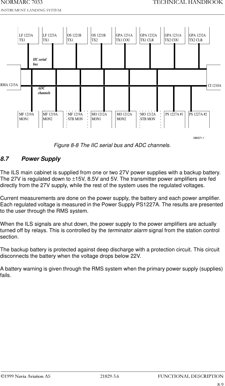
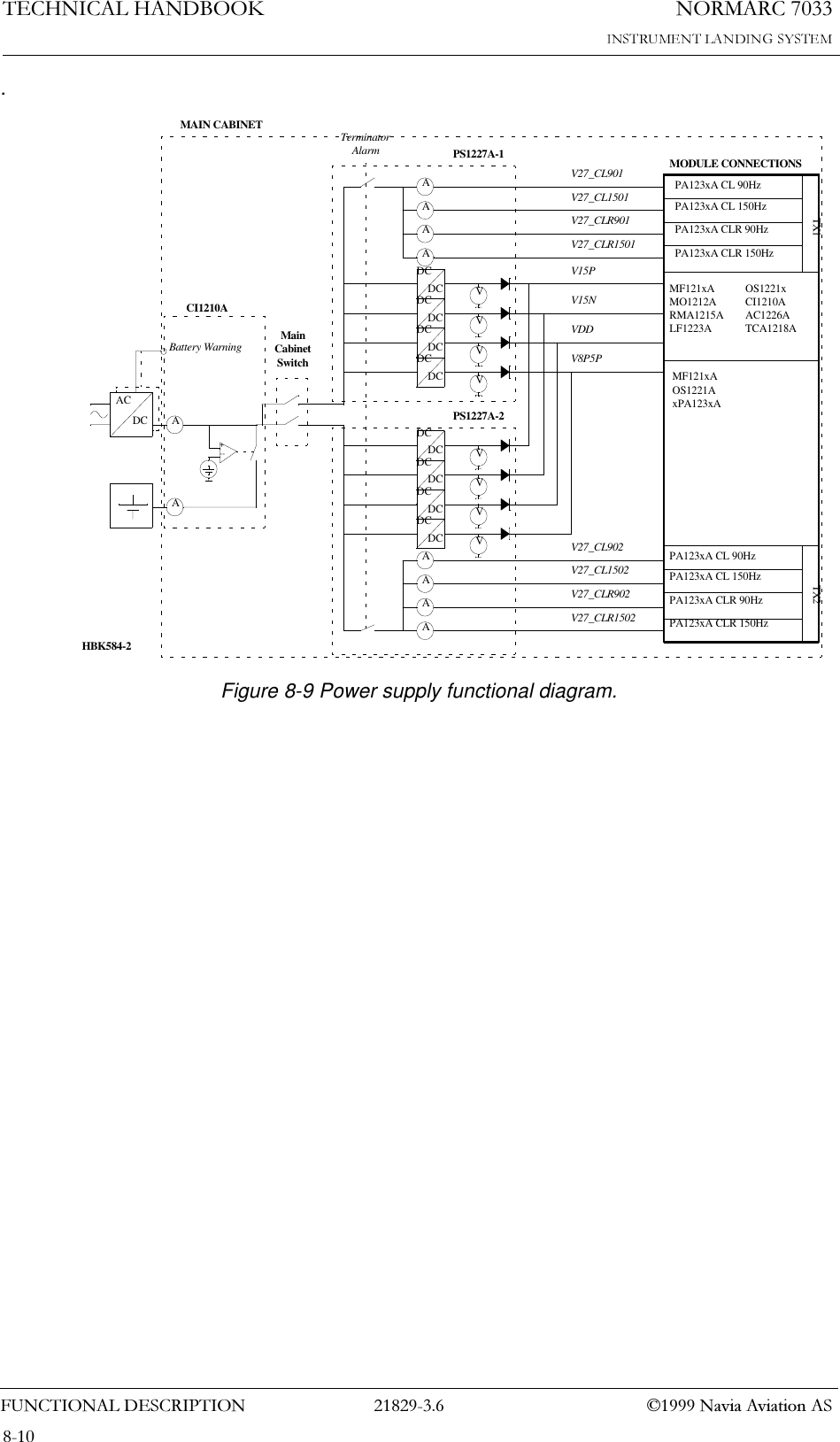
'(7$,/(''(6&5,37,211250$5&7(&+1,&$/+$1'%22.1DYLD$YLDWLRQ$6polled one by one. The event detect unit also has a built in integrity check. This function  works when the ILS is in normal operational mode (automatic mode with transmitters on and no alarm). When the ON/OFF is pressed, a  FORCE_AL signal is output. This signal turns off all transmitters (PA 1234A) without notifying the rest of the system. The loss of transmitted signal will be detected by the monitors (MO 1212) and cause monitor alarms to the STATION CONTROL.This alarm will result in a TX changeover initiated by STATION CONTROL, but since STBY TX is also turned off, monitor alarm will remain and cause TX shutdown after alarm delay. This sequence ensures that the monitoring circuits and shutdown mechanisms operates as intended. If the integrity check function should fail, a timeout function shuts the ILS down.INTERRUPT DETECTThis block detects transmitter state changes and stores the event causing the change. Trans-mitter feedback and coax relay position is also stored. An interrupt is generated to inform the RMS that a transmitter state change has occurred.TX 20 SEC DELAYThis function ensures that no transmitters are allowed to transmit for 20 seconds after an alarm shutdownhas occured.MAIN SELECT STOREThis block stores the information regarding which transmitter that is selected as main transmit-ter.INTERLOCK DELAYThis block turns on the transmitters 20 seconds after the interlock signal from the REMOTE CONTROL IF block has been deactivated.9.1.3.3 NMP106A  Station Control State Machine ControlGeneral Description:NMP106A is a FPGA within the STATION CONTROL block. It serves mainly as a state machine controller (states are stored in an EPROM) for transmitter on/off control. NMP106A is based on the Actel ACT1020 FPGA. For electrical specifications see the ACT1020 datasheet.Block Diagram:See Figure. 9-3Block Description:SEQUENCERThis block generates strobes and control signals for running the state machine. New states are triggered based on received new data from NMP105A (on the STO_BUS). This block also generates reset to the hardware watchdog safeguarding and controlling the station control reset.EVENT CHECKThis block checks event and main select signal received from NMP105A. Two identical event/main select signals must be received in sequence before the event/main select is acted upon.TIMER
1250$5&7(&+1,&$/+$1'%22.'(7$,/(''(6&5,37,21  1DYLD$YLDWLRQ$6Used by the state machine for delays/timeouts for state changes.DELAYDelays the coax relay position feedback in state change sequences. Ensures that the coax relay on COA1207A (Ch.9.1.6) will not change position while the transmitters are transmitting.PARITY CHECKThis block check the parity of each byte read from the state machine content EPROM. Parity failure results in transmitter shutdown.LOCKUP DETECTThis block detects failures in the state machine sequence. It will trigger if the state machine don’t become idle within a specified time. Failures results in transmitter shutdown.EPROM READ DATA ADDRESSThis block is an address counter setting the address for the state machine EPROM during reading through the RMS. The RMS can either reset or increment the adress counter. The feedback from these control strobes, address bit 0 and EPROM data byte are transferred to the NMP105A for reading by the RMS.TX ON/OFF CONTROLThis block controls the on/off state of the transmitters. Default is leaving the transmitters in the state reported by their feedback signals, thereby providing no change in transmitter state. However, if PARITY CHECK failure or event LOCKUPDETECT failure is detected, the trans-mitters are turned off.LOCAL LAMP STATUSLocal panel lamp outputs to the LOCAL CONTROL BLOCK are provided based on coax relay position, TX main select, transmitter status and station status received from NMP105A.EPROM ADDR MUXThis block selects EPROM addressing either for STATE MACHINE or RMS read control.9.1.3.4 NMP107A  Terminator General Description:NMP107A is a FPGA providing most of the TERMINATOR function. The terminator function is to provide a transmitter shutoff function if the STATION CONTROL should fail to do so. NMP107A is based on the Actel ACT1020 FPGA. For electrical specifications see the ACT1020 datasheet.Block Diagram:See Figure 9-3 and Figure 9-4.Block Description:RMS INTERFACEThe RMS interface provides the interface to the RMS BUS.RMS LEVEL DETECTThis block decodes RMS access levels 2 and 3 using access configuration in CONFIG block,
'(7$,/(''(6&5,37,211250$5&7(&+1,&$/+$1'%22.1DYLD$YLDWLRQ$6write disable switchlock information from LOCAL CONTROL, access grant from REMOTE CONTROL IF and access requests from the RMS.EVENT DETECTThe event detect unit checks for valid events (for example on/off-key, alarm, interlock etc.), and sends valid events to the terminator state check. Events not valid for the current mode of operation are ignored.TERMINATOR STATE CHECKThis block acts upon events/states received from the EVENT DETECT block. Alarm/interlock states are allowed to be active for 1 second before terminator alarm is activated. The termina-tor alarm is then reset if an on/off-event is detected, thereby starting a new 1 second timeout. The STATION CONTROL must now stabilise the ILS with no alarm within this 1-second period of time if a TERMINATINATOR shutdown should be avoided. If terminator is triggered by alarm or interlock while transmitters are transmitting, an interrupt is generated. The RMS can then read the cause of the interrupt through the RMS BUS.INTERLOCK FILTERThis block overrides the interlock signal in interlock override mode of operation. To enable interlock override mode of operation the interlock override switchlock must be activated, the local/remote switch must be in local position and the auto/manual switch must be in manual position.MON.1 ALARM & ERROR DETECTIONThis unit decodes the MON1 TRM ALARM BUS and generates alarm if the monitor MO 1212A no. 1 has set the alarm flag for any of the 32 parameters received in a set. Error checks includes parameter identity sequence check, AL_N negated of AL, test channel alarm toggling and timeout for RDY-signal. Any alarm/error will set the monitor alarm output (M1ALARM) for the duration of the next 32 parameters, meaning that 32 parameters without alarm/error must be received before the alarm output is reset.MON.2 ALARM & ERROR DETECTIONSame as for MON.1 ALARM & ERROR DETECTION but for MON2 TRM ALARM BUS.VOTINGThis block provides a monitor alarm (~VALARM) depending on jumper configuration (1 of 2 or 2 of 2 voting) in the CONFIG block and inputs from the two MO1212A monitors (not including STBY monitor). When configured for 2 of 2 voting both MO 1212A monitors must give alarm to set the ~VALARM output. When configured for 1 of 2 voting alarm from one of the two MO 1212A monitors is suffisient to set the ~VALARM.9.1.3.5 NMP109A  Remote Control InterfaceGeneral Description:NMP109A is a FPGA providing most of REMOTE CONTROL IF function. The NMP109A transfers data between STATION CONTROL and TERMINATOR and the remote control (via CI 1210A). NMP109A is based on the Actel ACT1020 FPGA. For electrical specifications see the ACT1020 datasheet.Block Diagram:See Figure 9-3 and Figure 9-4.
1250$5&7(&+1,&$/+$1'%22.'(7$,/(''(6&5,37,21  1DYLD$YLDWLRQ$6Block Description:STB LAMP FILTERThis block provides the standby lamp information to be sent to remote control by the TX UART.TX UARTConverts parallel data to 2-bytes serial messages. Protocol for the serial data SDOUT (sent I 1210A) is startbit, 8 databits, 1 stopbit, odd parity.RX UARTConverts serial data SDIN received from remote control (via CI 1210A) to parallel data (2 bytes).MESSAGE DETECTORMessages from RX UART are accepted only if two idnetical messages are received in sequence. If  so, the data output latch is updated and a new-message pulse is generated.NEW MESSAGE TIMERChecks whether an OK message from MESSAGE DETECTOR and carrier detect signal from CI 1210A is present. Missing message or no carrier detect for 2 seconds or more gives time-out signal to DATA FILTER.DATA FILTERIn case the NEW MESSAGE TIMER has signalled a timeout (indicating missing messages) this block will modify the data received from the MESSAGE DETECTOR by forcing the TX_OFF signal to on (configurable). If configuration enables interlock, the interlock signal is also forced active.
'(7$,/(''(6&5,37,211250$5&7(&+1,&$/+$1'%22.1DYLD$YLDWLRQ$6Figure 9-3 TCA1218A Block diagram part 1VOTING_CONFIGM1S_AL_IDM1_ALM1S_AL_NM1S_AL_RAWM1S_AL_RDYMSTBS_AL_RDYMSTBS_ALMON1 ALARM& ERRORDETECTION VOTINGSTB ALARMDETECTIONPUSH-BUTTONONESHOTSLCIN[14:0]MON1 SC ALARM BUSMON2 SC ALARM BUSSTBMON SC ALARM BUSM1_ALARMM1_ERRORVALARMM2_ALARMM2_ERRORSTB_ALARMLC_INB[14:0]SC MON DATA DETECTORNMP104AFrom MO1212From MO1212From MO1212SW1THCES/PUSHBUTTONSLEDSWARN     +STB LEDSLC_IN[10:0]LC1217ADEBOUNCELC_IN[14:11]CONFIGTRM CLOCKSEQUENCEREVENT CHECKTIMERDELAYEPROM READDATA ADDRESSPARITYCHECKLOCKUPDETECTTX ON/OFFCONTROLLOCAL LAMPSTATUSSEQUENCECONTROLEVENT NO USEDMAIN SELECT USEDEPROM READ DATATIMEOUTVALUETIMERTRIGTIMEOUT GONEEPROM READ DATASTATEMACHINEADDRESSCOAX POSEPROM ADDRPARITY ERRORDATA BYTESPENDINGEVENT NOLOCKTIMEOUTTXFBTXFBCOAXPOSSTATUS LAMPSMAIN SELECTSC STATE MACHINE CONTROLCONFIGURATIONSTO_BUSEPROM DATATXONLC_OUTCOAXPOSPENDINGST_BUSNMP106ARMSINTERFACERMSLEVEL DETECTEVENTDETECTINTERLOCKFILTERALARMAUTO-ONOFF-TXONOFFTERMI-NATORSTATE CHECKILOCK_INTALARM_INTMON1 ALARM& ERRORDETECTIONM1T_AL_IDM1T_AL_RDYM1T_ALM1T_AL_NM1T_AL_RAWVOTINGMON1TRMALARMBUSMON2TRMALARMBUSRMS_BUSCONFIGURATIONLC_INRI_BUS-TERM_ALTERM_INTTRM_RO_ALTRM_LC_ALNMP107ARMS LEVELRMS_STATUSRMS COMMANDSM1_ALARMM1_ERRORM2_ERRORM2_ALARMLC_IN[14:7,0]EPROMSC CLOCKSPSP~VALARM~LC_OUT[11:0]~LC_OUT[17:12]EPROMADDRESSMUXRCCONFIG123546789101112131415161718HBK 545A-2MON1 ALARM& ERRORDETECTIONM1T_AL_IDM1T_AL_RDYM1T_ALM1T_AL_NM1T_AL_RAWM2_ALM2S_AL_NM2S_AL_RAWM2S_AL_RDYMON1 ALARM& ERRORDETECTIONM2S_AL_ID
1250$5&7(&+1,&$/+$1'%22.'(7$,/(''(6&5,37,21  1DYLD$YLDWLRQ$6Figure 9-4 TCA1218B Block diagram part 2LC_OUT[11:0]LCO_CONDREMOTE CONTROL INTERFACE (RI)STB LAMPFILTER TXUARTDATAFILTERMESSAGEDETECTORNEW MESSAGETIMERRXUARTRI_BUSAUX_OUTRO_BUSAUX_INCNF[6,4,1,0]SDINMESSAGETIMOUTSDOUTLC_OUT[17:12]NMP109ALC02CONDRMS INTERFACELAMP STATUSGENERATIONRMS LEVELDETECTEVENTDETECTINTERRUPTDETECTTX 20 SECDELAYMAIN SELECTSTOREINTERLOCKDELAYDLYACTIVE4STO_BUSRO_BUS (TX)RMS_LEVELFORCE_ALSC_INTVALARMSTALARM PENDINGRMS_BUSM1_A/EM2_A/ERI_BUSNMP105APS1227SPFrom MB1203(P15)From CI1210To CI1210To MB1203(P15)COAX_POS To coax relayTo OS1221~TXON[3:0] 4SPSPSPTo RM1213SP~CS~RMS_LEVEL[1:0]To MO1212      LF1223~TXC_INT2 SC EVENT DETECTIONCOAXFBTXFB[3:0]TRM_RO_ALARMSC_TXCOND123541718161514131211109876HBK545B-2
'(7$,/(''(6&5,37,211250$5&7(&+1,&$/+$1'%22.1DYLD$YLDWLRQ$69.1.4 LF1223A Low Frequency GeneratorGeneral Description:LF1223A provides the audio signals to be modulated onto the carrier signal in the transmitter (AC 1226A).  The levels of the 90Hz, 150Hz, RF level and ident signals and the morse code of the ident signal are programmable from the RMS.  Block Diagram:See chapter 9.1.6.Block Description:DIGITAL SECTIONThe LF_DIG block provides the interface to the RMS, the parameter storage (EEPROM) and the analog section.  All sequencing and local parameter update is performed by this block. Most of the functionality of the DIGITAL SECTION is handled by the NMP110A FPGA described in chapter 9.1.4.1.ANALOG SECTION.All levels are controlled digitally through multiplying DACs (MDACs), and the AC levels are stabilized through AGC amplifiers.  The fine tuning of the phase between the 90 and 150Hz signals is done manually with potentiometers.  The morse code is keyed in an analog multi-plexer, and can be synchronized with a DME.RF level and ident (DC_IDENT), SDM and DDM (90/150Hz) are generated in the MDAC chain. Multiplication (m) in the MDACs are 0≤m<1.• The reference voltage is multiplied in the first MDAC to form the DC portion of DC_IDENT. The keyed 1020Hz sine wave is multiplied in an other MDAC to control the ident amplitude, this signal forms the IDENT portion of DC_IDENT signal.• The DC portion of DC_IDENT is multiplied in the third MDAC to form the modulation sum reference .• This modulation sum reference is split in two signals where one is modified by a fourth MDAC before they are compined again to form the modulation difference. 9.1.4.1 NMP110A Low Frequency Generator ControlGeneral description:NMP110A is a FPGA within the LF_DIG block. It provides the interface between the RMS and the local parameter storage and sequencing of the LF signals are performed here.  NMP110A is based on the Actel ACT1020 FPGA.  For electrical specifications see the ACT1020 datasheet.
1250$5&7(&+1,&$/+$1'%22.'(7$,/(''(6&5,37,21  1DYLD$YLDWLRQ$6Block diagram:Figure 9-5 NMP110A block diagram.Block description:FREQUENCY DIVIDERdivides the system clock (3.6864MHz) into 30Hz, 90Hz, 150Hz, 1020Hz, morse code tick length and morse code word length clock signals.IDENT SEQUENCERgenerates the programmed ident envelope for the ILS signal and external DME equipment.CONTROL SECTIONincludes the RMS interface, address decoding, configuration control and automatic refresh of the DACs and the other registers.  The refresh cycle is performed after a completed RMS access cycle.9.1.5 OS1221B RF OscillatorGeneral Description:The OS1221B module generates the RF signals used for the generation of the carrier signals in the transmitters (ch. 9.1.8).ConfigurationStorageCounterIdent SequencerRefresh AddressSequencerRMS interfaceDME_IDNT_IN, DME_ACTIVEAddressDecoderMUXEXT_SERVICE*_CS,DAC_AIOCSBCLKTST30CLR90CLR150COU90COU150IDNT_DIGDME_IDNT_OUTIDNT_ONIOS*IOD*ControlControl SectionFrequency DividerADDR*COAX_POS, LF_ADDRHBK563-1
'(7$,/(''(6&5,37,211250$5&7(&+1,&$/+$1'%22.1DYLD$YLDWLRQ$6Block Diagram:Figure 9-6 OS1221B block diagram.Block Description:The RF signal is generated by a voltage controlled oscillator (VCO) built around a Dual Gate Mosfet Transistor, chosen because of its good noise properties, and the possibility to have an isolated output at the drain.A part of the signal is fed back, via a buffer for isolation, to a divide by 64, modulus 2 pres-caler. This is connected to a MC145152-2, a phase locked loop circuit that performs the counting and control of the prescaler. The total count, and thereby the frequency, is set by inserting shunts onto an array of pins.The correct count for a desired frequency (FRQ) is found as follows:CHANNELSELECT COUPROGRAMABLEDIVIDERRFOSCILLATORPHASEDETECTORLOWPASSFILTER VCOLOCKDETECTWINDOWCOMP.BANDPASSFILTER12 dB OSC_COU_RF64MODULUS 2DIVIDERCOU Tx ON/OFFX-TALFREQ.TESTPOINTFREQUENCYADJUSTMODULUS SELECTLOCK DETECT TO IIC BUSSCHM.TRLATCHSCHM.TRLOCK DETECT TO IIC BUSLOCK DETECT TO IIC BUSCHANNELSELECT COUPROGRAMABLEDIVIDERRFOSCILLATORPHASEDETECTORLOWPASSFILTER VCOLOCKDETECTWINDOWCOMP.BANDPASSFILTER12 dB OSC_CLR_RF64MODULUS 2DIVIDERMODULUS SELECTLOCK DETECT TO IIC BUSSCHM.TRLATCHSCHM.TRLOCK DETECT TO IIC BUSLOCK DETECT TO IIC BUSCLR  Tx ON/OFF HBK587-3
1250$5&7(&+1,&$/+$1'%22.'(7$,/(''(6&5,37,21  1DYLD$YLDWLRQ$6COUNT = FRQ / 7.5011KHZIn order to set the frequency on the OS1221, the count must be rounded off to the nearest integer value and converted to a binary number.Insert shunts for binary zeros on the pin arrays P2 or P102 (COU/CLR) starting with the most significant bit on P2/102,A0 and the least significant bit on P2/102,N9. Be aware that most cal-culators discards leading zeros. Please find tables of jumper settings in Operating Manual Appendix B.The internal oscillator of the Course PLL is also used to control the Clearance PLL. The differential output of the phase comparator is made single ended by a balanced amplifier. A combined low-pass filter and integrator is built around an operational amplifier, that gener-ates the control voltage for the RF oscillator.  This control voltage is also fed to a window com-parator that alarms the system via the I2C-bus if it falls outside its limits  (another control of the PLL is via the Lock Detect output of the PLL).  The Lock Detect output of the PLL circuit is fed to a low pass filter and a transistor. This output consists of narrow negative going pulses when the loop is locked, and wide pulses of variable width when out of lock.  Therefore the transistor will be turned off when in lock, and on when out of lock.The output from the transistor goes to two Schmidt triggers, one latching and one unlatching. The latching Schmidt triggers turns the signal off if the loop goes out of lock and alarms the I2C-bus. It is reset by power on and/or a low transition of the COU_OFF signal (CLR_OFF for the clearance channel).  The other Schmidt trigger is used to inform the system of the situation that the loop have been out of lock, but is in lock at the present time even if the signal is turned off (this might be the situation if a short drop in the 12V supply occurs, or a change in fre-quency setting has taken place).The signal switching is done in two steps. The first is a diode switch and the next is a Dual Gate Mosfet transistor that can be turned off by taking its control gate to a low potential. This transistor acts as a buffer for the signal when in the on state. At the output of this transistor, a second order bandpassfilter follows, that serves as an output match of the transistor and to fil-ter out harmonics of the output voltage. The last stage is a 12dB gain block that delivers 10mW of power to the PC1225 card.The Clearance channel is identical to the Course channel ecsept for the crystal oscillator for the PLL.9.1.6 GPA1231A Glidepath Course Power Amplifier AssemblyGeneral Description:The Glidepath Course Power Amplifier Assembly GPA1231A consists of the following mod-ules mounted together as shown on Fig. 9-7.2 Power Amplifiers PA1234A1 Amplitude Control AC1226A1 Phase Control PC1225B1 Feedback Detector FD1236A1 Combiner Detector CD1238A
'(7$,/(''(6&5,37,211250$5&7(&+1,&$/+$1'%22.1DYLD$YLDWLRQ$6The GPA1231A receives RF signals and LF signals from the OS1221B Oscillator (Ch. 9.1.5)  and LF1223A low frequency generator (Ch. 9.1.4)  respectively. The outputs from the GPA1231A are carrier sideband (CSB) signal and sideband only (SBO) signal. Detected sam-ples of the CSB and SBO signals and the phase feedback signal are available on the BNC connectors on the front panel. Information about signals and status are interfaced with the RMS. Block Diagram:See  Figure 9-8 and Figure 9-9.Block Description:The PC1225B Phase Control receives the RF signal from the oscillator OS1221B and splits htis signal into two paths (90Hz and 150Hz branch). The RF phase regulator blocks ensure correct phase relationship between the 90Hz and 150Hz modulated RF signals prior to  com-bining them into CBS and SBO signals.The AC1226A Amplitude Control provides and controls the required LF modulation signals (90Hz and 150Hz) for the PA 1233A power amplifiers that keeps the output RF level and amplitude modulation constant.The PA1234A Power Amplifier modulates the incoming RF signal from PC1225B with a 90Hz or a 150Hz LF signal  to obtain an AM-signal and amplifies the modulated signals.The FD1236A Feedback Detector provides feedback signals for amplitude and phase correc-tion of the 90 and 150 Hz modulated RF signals.The CD1238A Combiner Detector combines the 90 Hz modulated RF signal and the 150 Hz modulated RF signal in such a way that true CSB and SBO RF signals are generated. In addi-tion, detected and filtered CSB and SBO signals for measurement purposes are provided to the test connectors on the front panel.Detailed description about the individual modules are found below.9.1.7 GPA1232A Glidepath Clearance Power Amplifier AssemblyGeneral description:The Glidepath Course Power Amplifier Assembly GPA1231A consists of the following mod-ulesThe GPA1232A contains the RF blocks in the GP Clearance transmitter system. It receives RF signals and LF signals from the OS1221B oscillator and LF1223A low frequency generator respectively. The output  of the GPA1232A is a carrier sideband (CSB) signal. Detected sam-ple of the CSB signal is available on the front panel. Other system parameters are transmitted to the RMA1215A.Block Diagram:1 Power Amplifier PA1234A1 Amplitude Control AC1226B1 Phase Control PC1225B1 Feedback Detector FD1224
1250$5&7(&+1,&$/+$1'%22.'(7$,/(''(6&5,37,21  1DYLD$YLDWLRQ$6See transmitter block diagram.Block Description:The PC1225B Phase Control receives the RF signal from the oscillator OS1221B. The RF sig-nal is fed into the 90Hz branch and further through buffers and amplifiers. The 150Hz branch is inactive.The PA1234A Power Amplifier modulates the incoming RF signal from PC1225B with a CBS LF signal  to obtain an AM-signal and amplifies it. The AC1226B Amplitude Control generates the required CSB LF modulation signal to the power amplifier, to keep the output RF level and amplitude modulation constant.The FD1224A  Feedback Detector provides a feedback signal for amplitude correction of the CSB modulated RF signal.9.1.7.1 PA1234A Power AmplifierGeneral Description :Power amplifier PA1234A is a three stage single-ended amplifier. The first stage works as an AM-modulator. The modulation tone (90Hz or 150Hz) is fed to the collector of a bipolar transistor. This modulation stage is operating in class C and has imped-ance matching network at both input and output. Nominal RF input level is approximate 20dBm.Second stage consists of a 5W MOSFET-transistor operating in class B. The input impedance network is matched to 50Ω, while the output impedance network is matched to the complex conjugated impedance of the third stage transistor. This stage has a collector-to-gate feed-back and a  input shunt loading resistor at the transistor gate, to prevent unwanted oscillations and keep the transistor unconditionally stable. Third stage is a 30W MOSFET-transistor operating in class AB. Its output impedance network consists of microstrip transmission lines and a variable capacitor to achieve maximum power and efficiency. This stage has also feedback and shunt resistors to prevent unwanted oscilla-tions. As gain control, both the second and third stage have potentiometers to set the operat-ing point. A positive voltage regulator is used to keep a fixed input voltage to these gain control circuits.The lowpass filter at the output is a 7th order filter,  giving better than 50dB attenuation of all harmonics and forward loss is less than 0.5dB. Filter input and output impedance are 50Ω.9.1.7.2 AC1226A Amplitude controlGeneral Description :The main purpose of the AC1226A is to maintain a constant modulation and RF level for the output signals from the PA 1234A power amplifiers. The RF level and modulation depths are derived from three reference input signals coming from LF 1233A. A DC reference level sets the RF level for both power amplifiers and one 90Hz and one 150Hz AC reference signal determines the modulation depths of the 90Hz and 150Hz power amplifiers respectively. The AC1226A also contains measurement circuits for the RMS.ADJUSTMENTS:The levels of the reference DC signal and the two reference AC signals are separately adjust-
'(7$,/(''(6&5,37,211250$5&7(&+1,&$/+$1'%22.1DYLD$YLDWLRQ$6able. In addition, the power balance between the two power amplifiers can be adjusted. The goal of these adjustments is to compensate various tolerances inside the GPA1231A. Adjusted correctly, any GPA1231A can be replaced by any other GPA1231A without any adjustments, and still be within specified limits.Any site or RF frequency dependent adjustments shall be made on the LF1223A module via the RMS system.FEEDBACK FUNCTION:The 90 and 150 Hz LF signals from LF1233A are combined with the DC (ident) signal also coming from LF1233A to form the desired RF envelope for each of the PA1234A. This enve-lope is compared with the envelope detected by FD1236A and the resulting signal is fed to the PA1234A modulator. This process eliminates any ground offset between the GPA1231A and the LF1223A generating the reference signals.MAINTENANCE MEASUREMENTS:Following measurements are reported to the RMS: The 22-28V DC power supply for each PA1234A.Detected CSB and SBO RF level.Peak of the phase correction curve.9.1.7.3 PC1225B Phase ControlGeneral Description:The RF carrier signal from OS1221B (Ch. 9.1.5) is split in two paths, one to be modulated with 150 Hz, and one to be modulated with 90 Hz. The first stage of each path is a phase regulator, with a range of ±100 degrees. In the 90Hz path, the phase is set with a potentiometer for ref-erence, in the 150Hz path the phase is controlled by a phase comparator. The phase compar-ator is a part of a negative feedback loop which ensures the correct phase relationship between the 90Hz and 150Hz modulated RF signals from the PA1234A power amplifiers prior to combining them into CBS and SBO. Each of the phase regulators is followed by a buffer amplifier, a 15dB gain block and a output stage.The RF level at the output is fed back in an automatic gain control feedback loop ensuring constant output level of 20dBm. 9.1.7.4 FD1236A Feedback DetectorGeneral Description:The function of FD1236A is to provide feedback signals for amplitude and phase correction of the 90 and 150 Hz modulated RF signals.  Two dual directional couplers sample the main RF signal from the 90 Hz  and the 150 Hz modulated power amplifiers, respectively. One half of each dual coupler is used for amplitude control, while the other half is used for phase control.For AMPLITUDE control, the sampled RF signal is detected by a diode that is slightly forward biased for linearity, bias being provided by another diode. The detector time constant is short; the detected signal consist of a positive voltage proportional to the RF carrier level and an LF voltage proportional to the modulation. When this output is fed back to the power amplifiers via the Amplitude Control board,  RF power and modulation depth will be held constant, and distortion will be practically eliminated.  A low-pass filter is inserted between the detector diode and the coupled lines to prohibit RF harmonics generated by the detector to couple back onto the main RF line. Coupler directivity is much improved by very small capacitances connected across the lines.
1250$5&7(&+1,&$/+$1'%22.'(7$,/(''(6&5,37,21  1DYLD$YLDWLRQ$6For PHASE control, a 90 degree 3 dB hybrid is used as a phase discriminator. Such a device has the property that the resulting amplitude at its outputs depend upon the phase difference at its inputs.  Here, the two sampled RF signals, which have equal amplitudes, are applied to the hybrid inputs. The two output signals from the hybrid are rectified, giving positive output voltages with some LF components. Normally, these two voltages will be equal. Any shift in RF input phase will make these voltages unequal. When these output voltages are fed back to the Phase Control board, the phase relations at the input will be held constant.  For equal magnitude at the outputs of the 90 degree 3 dB hybrid, the phase difference at the hybrid inputs must be zero. Proper phasing initially is here obtained by the insertion of a delay line in the 150 Hz modulated path. The main RF input signals applied to the couplers are already 90 degrees out of phase here, with the 90 Hz modulated signal lagging. Therefore, the additional delay line between the 150 Hz coupler and the hybrid will provide the missing 90 degree delay for zero phase difference at the hybrid inputs. A small trimming capacitor is included to facili-tate an offset to compensate for eventual minor phase errors in the remaining RF circuitry out-side the phase feedback loop. Adjustment can therefore only be done properly with the whole transmitter module working.  This trimmer is the only adjustable component on this board. All diodes used on this board are matched pairs for temperature stability reasons.The RF power output from this board is fed through a pair of 50 Ohm coaxial connections inside the housing directly to the Combiner board CD1238A, the connections being discon-nectable to facilitate removal for repair. Inserted in a properly adjusted transmitter module, the 90 and 150 Hz modulated output (and input) power signals of the Feedback Detector board will have equal amplitudes with the 90 Hz path lagging the 150 Hz path by 90 degrees (except for eventual offset), and this condition will be held constant by the feedback loops.9.1.7.5 FD1224A Feedback detectorGeneral Description :The function of FD1224A is to provide a feedback signals for amplitude correction of the com-posite 90 Hz and 150 Hz modulated RF signal for GP Clearance, and to provide a detected output of this signal for measurement purposes.A directional coupler samples the main RF signal from the power amplifier, which is modu-lated with both 90 and 150 Hz in this case.The sampled RF signal is detected by a diode that is slightly forward biased for linearity, bias being provided by another diode. The detector time constant is short; the detected signal con-sist of a positive voltage proportional to the RF carrier level and an LF voltage proportional to the modulation. When this output is fed back to the power amplifier via the Amplitude Control board,  RF power and modulation depth will be held constant, and distortion will be practically eliminated. This detected output voltage is also used for measurement purposes.A low-pass filter is inserted between the detector diode and the coupled lines to prohibit RF harmonics generated by the detector to couple back onto the main RF line. Coupler directivity is significantly improved by very small capacitances connected across the lines. No adjustable components are used on this board.9.1.7.6 CD1238A Combiner DetectorGeneral Description:The function of CD1238A is to combine the 90 Hz modulated RF signal and the 150 Hz mod-ulated RF signal from FD1236A to form the CSB and SBO RF signals to be transmitted. In addition, detected and filtered CSB and SBO signals for measurement purposes are provided to BNC test connectors on the front panel.
'(7$,/(''(6&5,37,211250$5&7(&+1,&$/+$1'%22.1DYLD$YLDWLRQ$6The 90 Hz and 150 Hz modulated RF input signals are of equal amplitude in phase quadra-ture, with the 90 Hz signal lagging. A 90 degree 3 dB hybrid is used as a combiner. When two RF signals of equal frequency and amplitude but with 90 degrees phase difference are applied to the two input ports of such a hybrid, the signals will add in phase at one output port but will be in reverse phase and cancel each other at the other port. This is the situation for the carrier frequency, resulting in twice the input power at the CSB port and no power at the SBO port. However, the sideband frequencies at the two inputs are not identical. The power of each sideband frequency will therefore be split equally between the two outputs. The resulting depth of modulation at the CSB output will be one half relative to the input value. At the SBO output, the two sidebands will be in reverse phase at the instant when the LF components are in phase. Thus true CSB and SBO signals are generated at the outputs.A pair of directional couplers sample the CSB and SBO RF output signals for measurement purposes. The RF samples are detected by matched diodes that are slightly forward biased. Detector filters have short time constant to preserve the LF envelopes. A low-pass filter is inserted between each detector diode and the coupled lines to prohibit RF harmonics gener-ated by the detector to couple back onto the main RF line. Coupler directivity is much improved by very small capacitors connected across the lines.
1250$5&7(&+1,&$/+$1'%22.'(7$,/(''(6&5,37,21  1DYLD$YLDWLRQ$6Physical OrganisationFigure 9-7 Physical organisation of power amplifier assembly.FD 1xxxxPA 123xx *)PC 1xxxxCD 123xx  *)AC 1226xC1 C2 C3 C4J16J15J1J2J3J10J11J12J13J7J6J8J14J9TP1 J17HBK695-2PA 123xx*) Not present in GP-CLR
'(7$,/(''(6&5,37,211250$5&7(&+1,&$/+$1'%22.1DYLD$YLDWLRQ$6    Figure 9-8 NM 7033 Transmitter Block Diagram part 1VOLT-AGEREF.DATA (7:0)DATA (7:0)DATA (7:0)CONTROLCONTROLCONTROLMODLEVELRFLEVELDDMDACDIFFER-ENTIALDISTRI-BUTIONIDENTKEYERIDENT + DC LEVELMOD 90 LEVELMOD 150 LEVEL (DC)LF_DIGDATA (7:0)CONTROLIDENT/VOICESELECTORVOICEVOICE ON/OFF ANALOGUE IDENT/VOICE90 HzLOWPASSFILTERAGCAMPLIFIER150 HzLOWPASSFILTERAGCAMPLIFIER 150 Hz COUANLG_IDLPF_1020LP FILTERMOD_AMPAGC_AMP2AGC_AMPLPF_150LPF_90DIGITAL AUDIOGENERATOR &CONTROLS3.6864MHzVrefVrefVrefVrefVOLT-AGEREF.DATA (7:0)DATA (7:0)DATA (7:0)CONTROLCONTROLCONTROLMODLEVELRFLEVELDDMDACDIFFER-ENTIALDISTRI-BUTIONIDENTKEYERIDENT + DC LEVEL MOD 90 LEVELMOD 150 LEVELDATA (7:0)CONTROL90 HzLOWPASSFILTERAGCAMPLIFIER150 HzLOWPASSFILTERAGCAMPLIFIER90 Hz CLR150 Hz CLRMOD_AMP2AGC_AMP4AGC_AMP3LPF_1502LPF_902VrefVrefVrefVrefLF1223A90 HZ COUCOUCLRDACDACDACUNREG 150 HzUNREG 90 HzUNREG 90 HzUNREG 150 HzRF BALBUFFERAC1226ACOMPA-RATORAMP_90MODU-LATIONCURRENTDRIVERAMP_90MODU-LATIONCURRENT DRIVERAMP_150COMPA-RATORAMP_150MOD DEPTH90 HzMOD DEPTH150HzDC(RF power)90 Hz FEEDBACK150 HzFEEDBACKAC1226A150 Hz CLRPHASE ADJ.90 Hz CLRPHASE ADJ.150 Hz COUPHASE ADJ.90 Hz COUPHASE ADJ.DATA (7:0)CONTROLRF BALBUFFERAC1226ACOMPA-RATORAMP_90MODUL-ATIONCURRENTDRIVERAMP_90MODUL-ATIONCURRENT DRIVERAMP_150COMPA-RATORAMP_150MOD DEPTH90 HzMOD DEPTH150HzDC(RF power)90 Hz FEEDBACK150 HzFEEDBACKAC1226BMOD 90 HzMOD 150 Hz150 Hz FEEDBACK90 Hz FEEDBACKMOD 90 HzMOD 150 Hz90 Hz FEEDBACK123456HBK 750A-1(RF POWER)(RF POWER)1 mm
1250$5&7(&+1,&$/+$1'%22.'(7$,/(''(6&5,37,21  1DYLD$YLDWLRQ$6   Figure 9-9 NM 7033 Transmitter Block Diagram part 2PC1225BRFPHASEREGU-LATORRF PHASEREGU-LATORAMPLIFIERAMPLIFIERMODU-LATOR DRIVER LOWPASSFILTERPA1234AMODU-LATOR DRIVER LOWPASSFILTERPA1234A90° HYBRIDRF PHASE ADJFD1236A90° HYBRIDCSB COUSBO COUCD1238AOS1221BSYNTHE-SIZERTx ON/OFFRF PHASE FEEDBACKRF PHASE FEEDBACKMODU-LATOR DRIVER LOWPASSFILTERPA1234ACSB CLRPHASEFEEDB.OFFSETADJ.PHASE OUTPC1225BRFPHASEREGULATORRF PHASEREGULATORAMPLIFIERAMPLIFIERPHASE OUTPHASEFEEDB.OFFSETADJ.FD1224A123456HBK 750B-1
'(7$,/(''(6&5,37,211250$5&7(&+1,&$/+$1'%22.1DYLD$YLDWLRQ$69.1.8 COA1207C Change-Over AssemblyGeneral Description:The COA1207C consists of one Change-Over Relay Assembly CRA1228A for the Course sig-nals and one Changeover Relay Unit CR1222A for the Clearance signals.The Change-Over Assembly for Course utilises two double-throw coaxial relays to connect the CSB and SBO output signals from either the main or standby transmitter (GPA1231A) to the antenna system or to a dummy load.  The assembly includes attenuators and phase shifters required to obtain the correct CSB/SBO relationship.For the CLR Signal: Only one relay is used as the GP CLR only consists of CSB.One CRA1228A is shown below. CR1228A contain the CSB circuitry only.Block Diagram: Figure 9-10 Changeover system block diagram.9.1.9 PS1227A Power SupplyGeneral Description:PHASER ATTENUATORCOAXRELAYCOAXRELAYOUTPUTSBOOUTPUTCSB MONITORCSBCOUPLERCOAX CONTROL50 ohm50 ohmPHASER ATTENUATORCOAX CONTROLCSB TX1CSBTX2SBOTX1SBOTX2HBK533-1
1250$5&7(&+1,&$/+$1'%22.'(7$,/(''(6&5,37,21  1DYLD$YLDWLRQ$6PS1227A supplies the NM 70xx cabinet with +27V, ±15V, +8.5V and +5V, from a +27V input.Block Diagram:Figure 9-11 PS1227A Block DiagramBlock description:The ±15V, +8.5V and +5V supplies are provided by integrated DC/DC converter modules.  PS1227A can operate in redundancy with a second power supply using or’ing diodes.  The output voltages are measured prior to these or’ing diodes, to be able to identify a power fail-ure.The four 27V outputs supply the GPA1231A power amplifiers. The current drawn are con-verted to a voltages used for current measurement. The ILS output signals may be shut down by cutting off the 27V supplies.  This is done by the TERMINATOR alarm signal (TRM_AL) (Ch. 9.1.3.4).9.1.10 RMA1215A RMS AssemblyGeneral descriptionThe RMA1215A is a microprocessor based assembly that contains the RMS software, and also forms the basis for the NM7000 RMM system. The RMA1215A consists of KD1214A  front panel with keyboard and display, and the RM1213A the RMS module.DCDCTRM_ALV27PGNDAAAAV27_CL90V27_CL150V27_CLR90V27_CLR150I27_CL90I27_CL150I27_CLR90I27_CLR150V15PV15P_MEASV15NV15N_MEASV9PV9P_MEASVDDVDD_MEASSYNCDCDCDCDCDCDCHBK565-1
'(7$,/(''(6&5,37,211250$5&7(&+1,&$/+$1'%22.1DYLD$YLDWLRQ$6Block Diagram:Figure 9-12 RMA1215A Block Diagram.Block description.CPUThe CPU is an 80C188EB micro controller with address decoding unit and two UARTs. Only one of these UARTs is utilised for serial communication. The other has been mapped as a par-allel IO port. The operating frequency of the CPU is 20 MHz provided by an external 40 MHz oscillator.WATCHDOG AND BATTERYA watchdog resets the CPU at power up and if the CPU does not toggle the watchdog reset bit within app. 1.6 sec. intervals, or if the +5V supply voltage goes below the battery voltage. In the latter case battery voltage will beconnected to the RAM and RTC. Removal of the battery or jumper P2 will cause the RESET line to go low and inhibit any function on the module. If a battery is not available, function can be achieved by shorting the battery socket.The battery can be disconnected by removing jumper P2 when the module is being stored.The battery voltage is measured using an opto coupler switch in order not to discharge the battery.  The battery providesapproximately one month memory retention at continuous use (system power turned off).INTERRUPT CIRCUITRYThe interrupt circuitry combines several interrupts into the 5 interrupt inputs of the CPU.DISPLAYThe display used is a 20 characters by 4 lines LCD.KEYPAD +-Identspeaker channels.IIC busInterruptsAnalogvoltagesDet.identJumperCPUCTRLportCTRLportCTRLportRMS busDoubleUARTCTRLportAnalogMUXAnalogMUXAnalogMUXInterruptcircutryCTRLportADKeypadDisplayKD1214ARM1213A WatchdogIICcontrollerBatteryRESETMemoryRAMEPROMEEPROMReal timeclockRS232driversThree serialHBK588-1
1250$5&7(&+1,&$/+$1'%22.'(7$,/(''(6&5,37,21  1DYLD$YLDWLRQ$6The keypad consists of seven pushbuttons, directly connected to a parallel input port.DOUBLE UARTThe dual UART is a standard UART with a 16 byte bidirectional FIFO on both channels.RS232 DRIVERSThe RS232 drivers are single supply RS232 drivers. They provide the interface between the UARTs and external PCs and modems.IIC CONTROLLERThe IIC controller handles the communication on the IIC bus which is the main communication ubs for maintenance data collection in the NM 70xx ILS.REAL TIME CLOCKThe real time clock keeps track of the date and time. Date and time is used to timestamp mon-itor and maintenance data sets. The RTC accuracy is better than 15 seconds per 24 hours.CTRL PORTThe CTRL ports in the block diagram are parallel IO ports for the CPU.ANALOG INTERFACEThe analog interface block contains two analog multiplexers and an A/D-converter. The main function of this block is to measure analog signals provided from several measurement points in the NM 70xx equipment. The analog multiplexers are connected to the same address bus with separate enable bits. This allows the analog inputs to be measured separately as single ended signals, or to be paired for differential measurements. AURAL IDENTThe Aural ident block contains an analog MUX, an amplifier and a loudspeaker. It enables the user to listen to the ident morse code from each of the four transmitters. The Det. ident inputs are detected CSB signal, filtered through a 1020Hz bandpass filter.MEMORYThe memory block contains RAM for data storage, EPROM for the program and EEPROM for permanent system setup parameters. The RAM has battery backup in order to retain logging data during a power down.9.1.11 CI1210A External Connection InterfaceGeneral Description:The CI1210A External Connection Interface board provides all the interface for the NM 70xx equipment for external connections exept from RF signals and power supply.The module performs transient overload protection on all inputs.  In addition CI1210A contains of a battery protection and a modem demodulation circuit.  The external connections are:• 1 Remote control port (FSK and opt. RS 232)• 3 RS232 ports (local and remote RMM)• 4 DC-loops (antenna cable fault detection)• 1 DME (keying synchronization)• 2 Temperature sensors (indoor/outdoor)
'(7$,/(''(6&5,37,211250$5&7(&+1,&$/+$1'%22.1DYLD$YLDWLRQ$6• 1 AC-level measurement input• 3 Differential Analog inputs• 8 Auxilliary Digital Inputs/OutputsBlock Diagram:Figure 9-13 CI1210A Block diagram9.1.12 MB1203A Monitor Section MotherboardDescription:MB1203A is the backplane for the 19” subrack in the NM 70xx cabinet. MB 1203A is a passive motherboard that provides all interconnections between the printed circuit board in this sub-rack and all interface for external signals exept from RF (Coax) cabling.+-AAPSModemMUXTOUTDOORTINDOORVACP/NANLG3P/NANLG2P/NANLG1P/NEAMX*AIN*USER_DIG*FSK*SD*,CDVPOWVBATTV27PIIC*[RS232]DL_*[RS232]DL_*Over-VoltageProtection*DME*DME_*HBK532-1
1250$5&7(&+1,&$/+$1'%22.'(7$,/(''(6&5,37,21  1DYLD$YLDWLRQ$6Table 9-1 MB1203A plug in module connectors.9.2 Tower EquipmentThe following paragraphs describes the modules to be located in the control tower.9.2.1 RCA1240C Remote Control AssemblyGeneral Description:The RCA1240C remote control assembly consists of the remote control RC1241A and front panel RF1242A, and provides the user interface to the ILS Cabinet from the control tower or technical equipment room. The RCA1240C is connected to the ILS cabinet either using ordi-nary telephone lines or using the RS232 interface selected by jumper plugs on the RC1241A.The telephone line interface conforms to V.21 standard (300 baud FSK) for use with ordinary 2-wire 600 ohm telephone line. The transmitter level is -10 dBm, and the receivers dynamic range is from -10 dBm to -34 dBm.Most of the functionality of the remote control is provided by the FPGA NMP128A described in chapter 9.2.1.1.Section #ModuleMonitor 1 1MO 1212A1MF 1211A1External Frontend 1Monitor 2 1MO 1212A1MF 1211A1External Frontend 2Standby Monitor 1MO 1212A1MF 1211AStation Control 1TCA 1218ARMS 1RMA 1215ATransmitter 1 1LF 1223A1OS 1221 A/BTransmitter 2 1LF 1223A1OS 1221A/BPower Supply 2PS 1227A
'(7$,/(''(6&5,37,211250$5&7(&+1,&$/+$1'%22.1DYLD$YLDWLRQ$6Block Diagram:Figure 9-14 Block diagram RCA1240CBlock schematic signal description:Block Description:CONTROL AND UARTSThis block interprets serial data from the ILScabinet and generates status outputs to front panel LEDs, slave panel outputs, opto outputs and buzzer signal based on the received sta-tus. Failure in data from ILS results in alarm condition. Discrete inputs from the front panel keyboard, control/AUX inputs and slave panel (Ch. 9.2.5) are collected and sent fo the ILS rack as serial data. INTERFACE SELECTThese straps selects between telephone line and RS232 for interface with the ILS cabinet. The default setting is line interface.LINE DRIVER/MODEMThis block converts logic level serial signals to and from FSK level line signals.RS232 DRIVERThis block converts logic level serial signals to and from RS232 level signals.SIGNAL DRIVERSThis block drives the front panel LEDs, opto outputs and slave panel LEDs.CONTROL INPUTS ILS control signals. Consists of INTERLOCK and TX_OFF.OPTO OUTPUTS Optocoupler outputs. Collector/emitter for ALARM, NORMAL, WARNING and STB_ALARM.SLAVE_DIRECT_BUS Data interface to optional slave panel. Consists of open col-lector outputs (ALARM, NORMAL, WARNING, STB_ALARM and SLAVE_BUZZER) and active low inputs (ON_OFF, CHANGEOVER and SILENCE).Linedriver/modemTelephonelineControlanduartsLED OUTPUTSRC1241ARS232driverRS232SignaldriversSLAVE DIRECT BUSRF1242A/BFront panelLEDsAUX_IN AUX_OUTKEYBOARD INPUTSRF1242A/BKeys andswitchesCONTROL INPUTSSLAVE DIRECTINPUTSSLAVELEDOUTPUTSOPTO OUTPUTSInterfaceselect&configRST_SL_AURAL_ONLYSTATUSALARMRST_RC_AURAL_ONLYHBK546-2
1250$5&7(&+1,&$/+$1'%22.'(7$,/(''(6&5,37,21  1DYLD$YLDWLRQ$6FRONT PANEL LEDSThis block contains the front panel LEDs used to indicate the operational status of the ILS.KEYS AND SWITCHESThis block contains the pushbuttons and switches used for operator input.9.2.1.1 NMP128A  Remote ControlGeneral Description:NMP128A is a FPGA proiding most of the remote control function. NMP128A is based on the Actel ACT1020 FPGA. For electrical specifications see the ACT1020 datasheet.Block Diagram:Figure 9-15 Block diagram NMP128ABlock Description:COMMAND MIXERThis block mixes the on/off and changeover commands from the different sources (remote control front panel or slave front panel input).TX UARTConverts parallell data to 2-bytes serial messages. The protocol is start bit, 8 data bits, 1 stop bit, odd parity.RX UARTConverts serial data from remote control to parallell data (2 bytes).RXuartSERIALDATAINNew messagetimerMessagedetectorLED&buzzerfilterCHANGEOVER_KEYTXuart SERIALDATAOUTAUX_INRC_BUSPARITY ERRORMESSAGE DATA LED OUTPUTSNEW MESSAGEMESSAGETIMEOUTMESSAGE DATACARRIERDETECT SLAVE LEDSON_OFF_KEYSLAVE_ON_OFF_KEYSLAVE_CHANGEOVER_KEYCommandmixerON_OFFCHANGEOVERINTERLOCKACCESS_GRANT_SWITCHTX_OFFAUX_OUTALARM BUZZERSLAVE BUZZERSILENCE_KEYSLAVE_SILENCE_KEYRST_RC_AURAL_ONLY564 2
'(7$,/(''(6&5,37,211250$5&7(&+1,&$/+$1'%22.1DYLD$YLDWLRQ$6MESSAGE DETECTORMessages are accepted only if two equal messages are received in sequence. If  so, the data output is updated and a new-message pulse is asserted.NEW MESSAGE TIMERChecks that an OK message and carrier detect is present. Missing message or no carrier detect for 2 seconds or more gives timeout.LED & BUZZER FILTERData from the ILS cabinet is filtered according to the following descriptions :• Missing data from ILS sets an alarm condition (Alarm LED on, all other off).• Activating SILENCE-key turns on all LED’s (lamptest).• Interlock turns off all LEDs.Buzzers are activated at transitions from normal to alarm. Lamptest always activates buzzers. Pressing SILENCE-key deactivates the local buzzer. The remote control SILENCE-key may deactivate the slave panel buzzer, while SILENCE from the slave panel may deactivate the local buzzer (both separately configurable).9.2.2 Motherboard MB1346A MB1346A is a motherboard for RCA1240C. InterconnectionsJ1 Backplane connector for RCA1240CJ2 RS-232 interface for external line modems, radio modems or fibre optic con-nections (alternative to P9 line connection).P3 Parallell interface to slave panel or status unit.P4,P5 Power supply connectorsP6 Aux in/out signals. May be used for FFM status, intruder alarm or other aux-iliary functionsP7 Opto coupler outputs for ALARM, NORMAL, WARNING and STB. ALARM.P8 Interlock connector (alternative connector located on slave panel) P9 RC telephone line interface. Includes alarm output and off input to establish automatic shutdown of GP when LLZ is off.NOTEWhen MB 1346A is used with RCA 1240C and Interlock function is not used (connected), a jumper plug must be installed in P8 (or P2 on SF1344A on Slave Panel).9.2.3 Power Supply PS635BDescription:PS635B is based on a switch-mode DC/DC converter module (PKA 2212) that features shut-down at low input voltage and current limiting of outputs ( short circuit proof).  Supply inputs are protected by a fuses.9.2.4 Motherboard MB1347ADescription:MB1247A motherboard provides the interface to PS635B power supply (Ch. 9.2.3) through connectors for 24VDC input and 5VDC output.
1250$5&7(&+1,&$/+$1'%22.'(7$,/(''(6&5,37,21  1DYLD$YLDWLRQ$69.2.5 Slave Panel SF1344A and SP1394ADescription:The SF1344A and SF1394A slave panel provides user interfaces to the ILS from the control tower or equipment room. The slave panels are connected to the RCA 1240C remote control assembly (Ch. 9.2.1) handling the interface with the ILS cabinet. SF 1344A and SF 1394A are identical apart from mechanical dimensions.FRONT PANEL LEDSLEDs on the front panel indicate the ILS status (Alarm/Warning/Normal)BUZZERThe internal buzzer provides aural alarms.PUSHBUTTONSPushbutton switches provides the on/off and silence (aural alarm reset) function.  The silence button is also used for lamp test.INTERLOCK CONNECTORA connector is provided for interfacing a IL 1379/IL 1380 interlock switch (Ch. 9.2.6).9.2.6 IL1379 / IL1380 Interlock switchDescription:The interlock switch is used if the runway has two ILS’s for opposite runway directions that shall be interlocked.The interlock switch consists of a key-operated change-over switch, and is connected to the RCA1240C remote control (Ch. 9.2.1) or SF 1344A/SF1394A slave panels (Ch. 9.2.5) of the affected localizer and glidepath equipment.IL 1379 and IL 1380 are identical modules apart from mechanical dimensions. The IL 1379 is 3 height units by 10 length units (app. 12,8x5cm). The IL1380 is 2 height units by 9 length units (app. 8,4x4,5cm).
'(7$,/(''(6&5,37,211250$5&7(&+1,&$/+$1'%22.1DYLD$YLDWLRQ$6 Figure 9-16 Interlock switch connections
1250$5&7(&+1,&$/+$1'%22.'(7$,/(''(6&5,37,21  1DYLD$YLDWLRQ$6
3$576/,6761250$5&7(&+1,&$/+$1'%22.1DYLD$YLDWLRQ$610 Parts Lists10.1 IntroductionThis section contains a tabulation of electrical and certain mechanical assemblies and parts; i.e. chassis-mounted  components, circuit cards assemblies, and modules of the equipment to the lowest replaceable unit (lru).10.1.1 Explanation of Parts Lists Form• Symbol/Item No.: References the symbol og item no. for each replaceable electronic part in the equipment.• Fig. No.: Lists the figure no of the illustration in which the part is shown.• Manufactorers Part No.: Navia Aviation part no.• UOC: Usable on Code: Lists the code assigned to equipment model numbers and identifies the components used in each model configuration. Se Usable On Code Index.
1250$5&7(&+1,&$/+$1'%22.3$576/,676  1DYLD$YLDWLRQ$610.2 Parts Lists     Electronics Subsystems GroupSymbol/ Fig. Manufactorers Qty./Item No. No. Description Part No. UOC UOCNM 7033 10-4 NM 7033 GP CABINET 18884 B -10-4   GCA 1249A GP 2-FRQ.  CAB. ASS. 18523 B -F1, F2 10-4              CIRCUIT BRAKER 13385 D2T7 10-4               FUSE 13368 D1C1 10-4               CAPASITOR 10533 D 1M2 10-4              COVER PLATE 14874 D2M1 10-4               FRONT PANEL,TOP 14861 D1M3 10-4               FRONT PANEL 14837 D1M4 10-4               COLLAR SCREW 12681 D16SPL 10-5               POWER SPLITTER 11553 D4AT1T, AT2T 10-5               ATTENUATOR 11721 D 2MF 1219A 10-4     MF 1219A GP MONITOR FRONT END 18584 D 2PS 1227A 10-4     PS 1227A POWER SUPPLY 18615 D 2OS 1221B 10-4     OS 1221B GP RF-OSCILLATOR 18594 D 2MO 1212A 10-4     MO 1212A MONITOR  18567 D 2MB 1203A 10-5        MB 1203A MOTHERBOARD 18540 D 1TCA 1218 10-4     TCA 1218A TX CONTROL ASSY. 18510 D 1RMA 1215A 10-4     RMA 1215A RMS ASSY. 18509 D 1LF 1223A 10-4     LF 1223A LF-GENERATOR 18601 D 2COA 1207C 10-5     COA 1207C  LLZ 2-FRQ. CHANGEOVER ASS. 18508 D -CRA 1228A 10-5        CRA 1228A LLZ & GP CHANGEOVER R. 18513 D 1AT1, AT2 10-4                ATTENUATOR 11729 D 2RL1, RL2 10-5                RELAY 13124 D 2DL1 10-5                DUMMY LOAD 10602 D 1DL2 10-5                DUMMY LOAD 10604 D 1 PH 449C 10-4             PH 449C PHASER 16587 D 2DC 420C 10-5        DC 420C DIRECTIONAL COUPLER 16577 D 2CR 1222A 10-5        CR 1222A CHANGEOVER RELAYS 18597 D 1DL1 10-5                DUMMY LOAD 10604 D 1RL1 10-5                 RELAY 13124 D 1GPA 1231A 10-4     GPA 1231A GP COU POWER AMP. ASSY. 18516 D 2GPA 1232A 10-4     GPA 1232A GP CLR POWER AMP. ASSY. 18517 D 2CI 1210A 10-3        CI 1210A CONNECTION INTERFACE BOARD 18561 D 1F1, F4 10-3              FUSE 13362 C 2J8, J21, J26 10-3             CONNECTOR 12408 C 3J9 - J17, J20 10-3             CONNECTOR 12406 C 10J27-J29 10-3             CONNECTOR 12406 C 3BC 1361B BATTERY CHARGER 18721 B 1BATTERY CHARGER 15048 B 2BATTERY 85Ah 15004 B 2BATTERY FUSE 14991 B 2RCA 1240C REMOTE CONTROL 21342 E 1    RC 1241B REMOTE CONTROL 21330 E 1SKA 1229A SERVICE KIT ASSY. 18514 B -    EB 1349A EXTENSION BOARD 18700 B 1    EB 1245A COAX CABLE EXT. BOARD 18662 B 1
3$576/,6761250$5&7(&+1,&$/+$1'%22.1DYLD$YLDWLRQ$610.3 Usable on code index10.4 FiguresFigure 10-1 Intensionally omittedFigure 10-2 Intenionally omitted Figure 10-3 Normarc 7011 & 7033 LLZ & GP cabinet, wall mount sideUSABLE ON CODE INDEXUsable On Code Description Navia Aviation Part No.ANM 7011 LLZ CABINET 18881BNM 7033 GP CABINET 18884CLCA 1246A LLZ 2-FRQ. CAB. ASS. 18520DGCA 1249A GP 2-FRQ.  CAB. ASS. 18523ETOWER EQUIPMENT -CI 1210ATerminal block forpower and battery connectionand decoupling capacitorT07 C01HBK1148-1J13J12J14J15J16 J28J17 J27J11J10J8J21J26J29J20J9
1250$5&7(&+1,&$/+$1'%22.3$576/,676  1DYLD$YLDWLRQ$6  Figure 10-4 Normarc 7033 GP cabinet11LF 1223AOS1221BCOA 1207CMO 1212AMF 1219APS 1227AGPA 1231ARMA 1215ATCA 1218AGPA 1232AHBK 1146-1F1, F2 M1*), M4M2*), M4M3*), M4M2*), M4*) FRONT PANELS NOT SHOWNPH 449CAT1AT2
3$576/,6761250$5&7(&+1,&$/+$1'%22.1DYLD$YLDWLRQ$6 Figure 10-5 Normarc 7033 GP cabinet, Rear viewSBO 1IN IN OUTSBO 2 SBODUMMY OUTSBO CSBDUMMY INCSB SBO 1IN OUTSBO 2 SBODUMMY OUTSBO CSBDUMMYCSBMB 1203COA 1207CTX1CLTX2CLTX1CLRTX2CLRAAVIEW A-AHBK1147-1DC 420ADC 420CDL1CRAT1TAT2TDL2DL1CR 1222A CRA 1228ARL1CR RL2 RL1SPL
1250$5&7(&+1,&$/+$1'%22.3$576/,676  1DYLD$YLDWLRQ$6
&86720(56,1)250$7,211250$5&$7(&+1,&$/+$1'%22.1DYLD$YLDWLRQ$63$57,9$33(1',;(6A Customers Information
1250$5&7(&+1,&$/+$1'%22.&86720(56,1)250$7,21  1DYLD$YLDWLRQ$6$
&86720(56,1)250$7,211250$5&$7(&+1,&$/+$1'%22.1DYLD$YLDWLRQ$6WHAT’S YOUR OPINION?We here in Navia Aviation want to do our utmost to meet the expectations and needs of the most important people in the world to us - you, our customers.We will be in contact now and again to make sure you are still satisfied with our products and our service.But, please don’t wait for us! Any time you might have a complaint (or compliment) or sugges-tions as to how we could serve you better, we would appreciate receiving your comments on the enclosed form - be it about our delivery, product specifications, operation, maintenance, service, or our performance in general.We take your opinions seriously, and will confirm receipt of your comments and keep you advised of any resulting actions.Yours Sincerely,Linda RøsslandCustomer Service
1250$5&7(&+1,&$/+$1'%22.&86720(56,1)250$7,21  1DYLD$YLDWLRQ$6$
&86720(56,1)250$7,211250$5&$7(&+1,&$/+$1'%22.1DYLD$YLDWLRQ$6   Product Report Please forward to:Customer Service Dept. CS - No.:Customer / company: Name:  Received by: Date:Address: Phone: Fax number: E-mail:Site of installation: Contract number: Navia order No.: Warranty expires:Product: Serial No:Fault description / symptoms: Attachement:
1250$5&7(&+1,&$/+$1'%22.&86720(56,1)250$7,21  1DYLD$YLDWLRQ$6$
&86720(56,1)250$7,211250$5&$7(&+1,&$/+$1'%22.1DYLD$YLDWLRQ$6CustomerNotification of Goods in TransitCustomer’s Engineers to:Form to be faxed prior to shipment to NAVIA AVIATION AS, Customer Service Dep.(Fax No. . +47 23 18 02 13)   Sender’s Name:................................................... Tel: .......................................................  Site: .....................................................                 Fax: ......................................................  Return Adress:.......................................................................................................................  Consignee:  NAVIA AVIATION AS  P.O. Box 50, Manglerud  N-0612 Oslo                                                        Tel: +47 23 18 02 00  NORWAY.                                                              Fax: +47 23 18 02 13Carrier’s Name: ..................................................... Date of Shipment: .............................Carrier’s Ref No: ................................................... Number of Packages: .............................The following item(s) will be sent for repair under Maintenance Contract No.  ____________Item Description Quantity Part Number Serial Number12345NAVIA AVIATION AS:Please fax acknowledgement of goods received (including date received) to:__________________
1250$5&7(&+1,&$/+$1'%22.&86720(56,1)250$7,21  1DYLD$YLDWLRQ$6$

Navigation menu