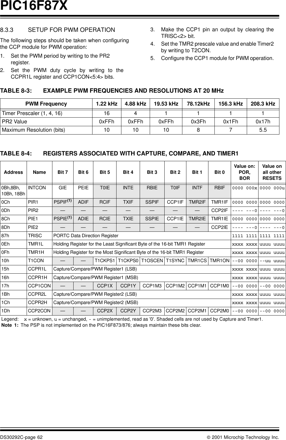
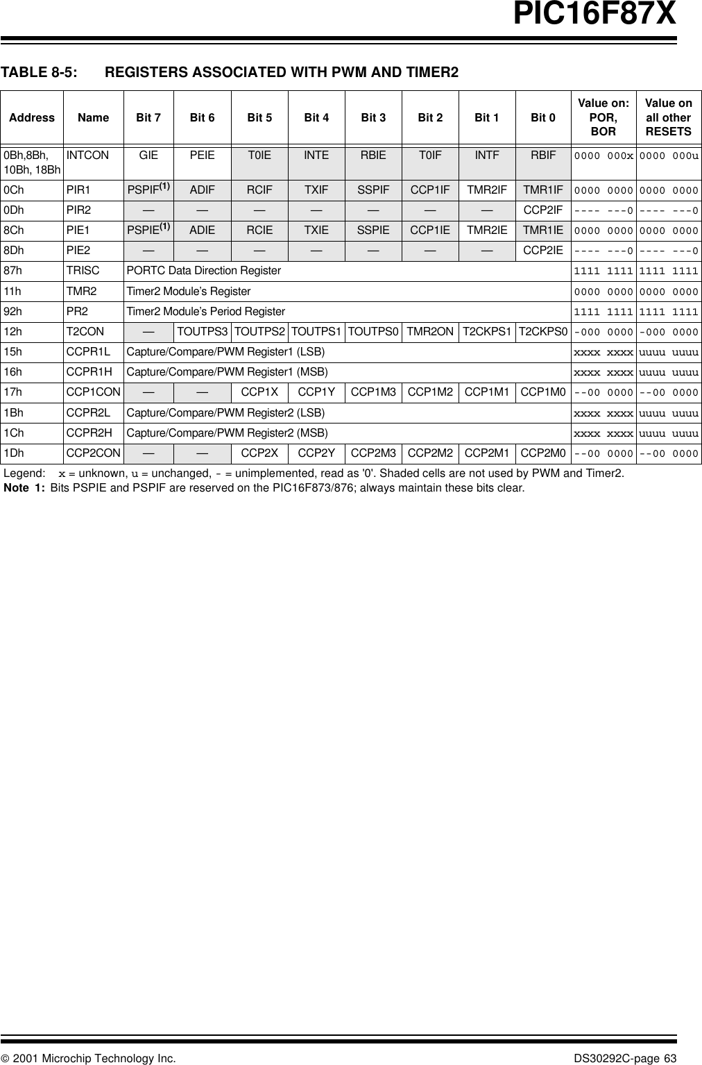
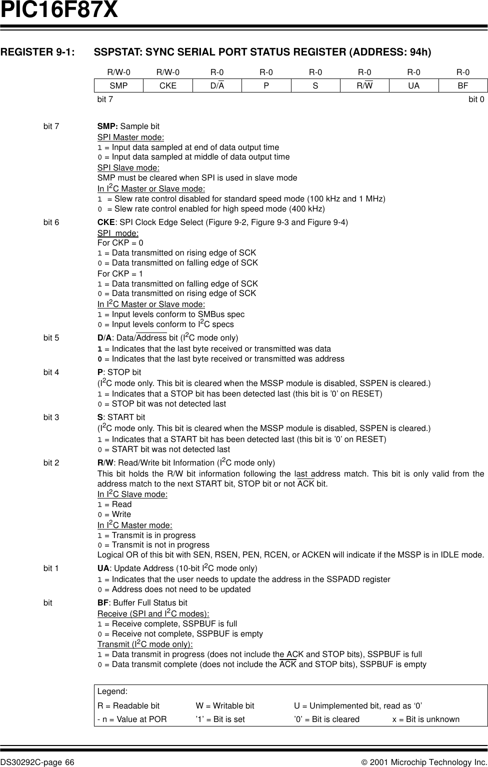
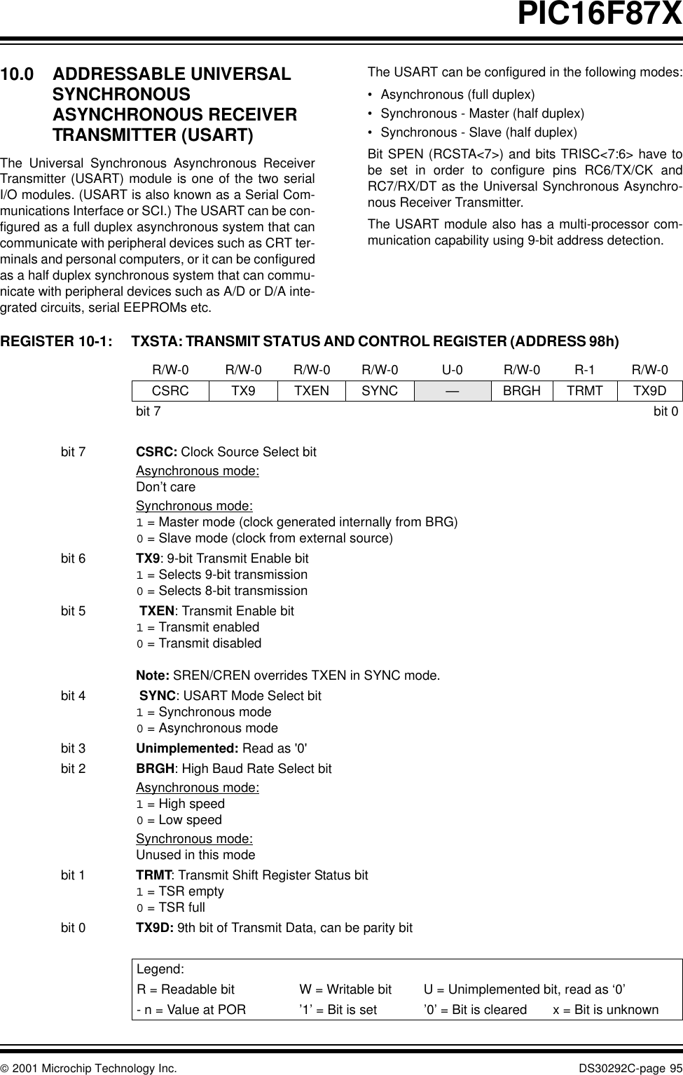
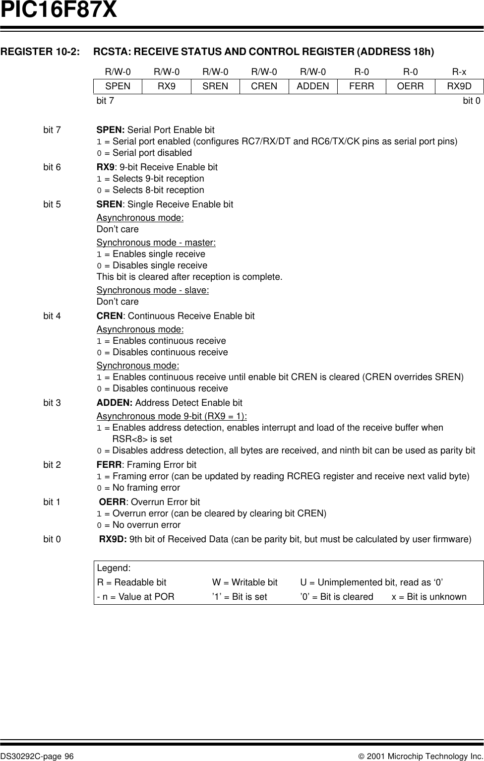
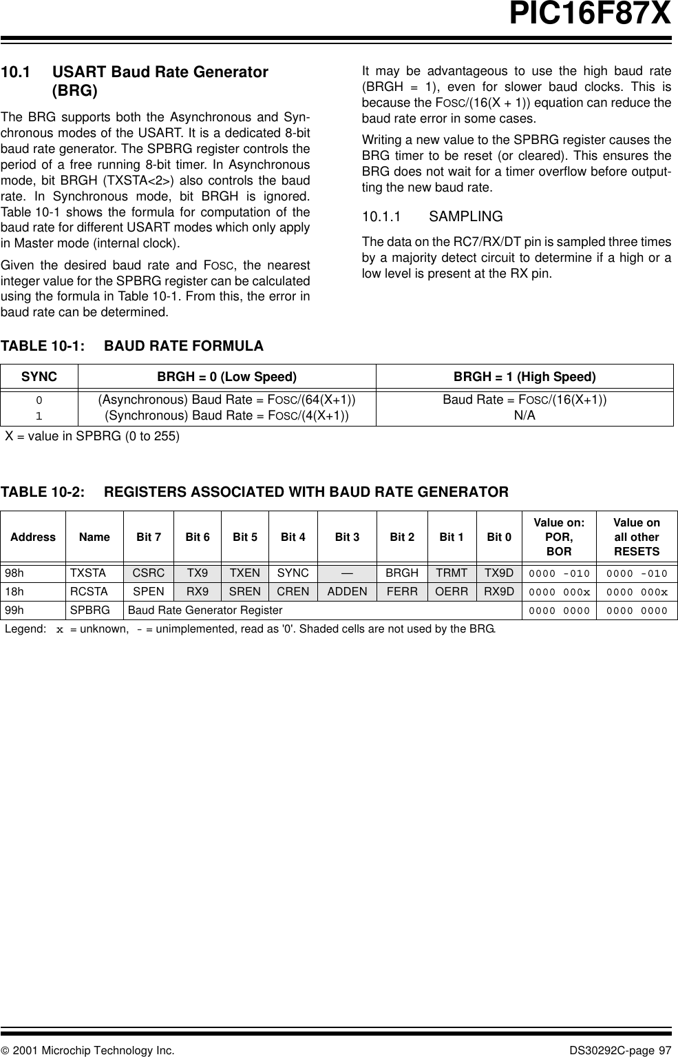
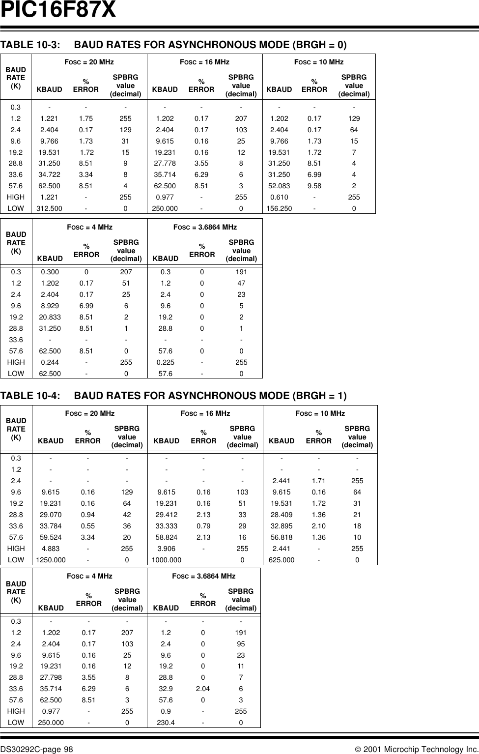
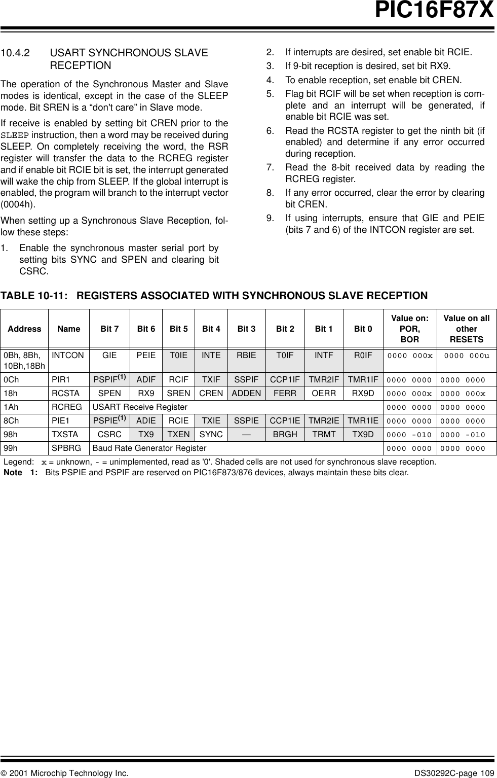
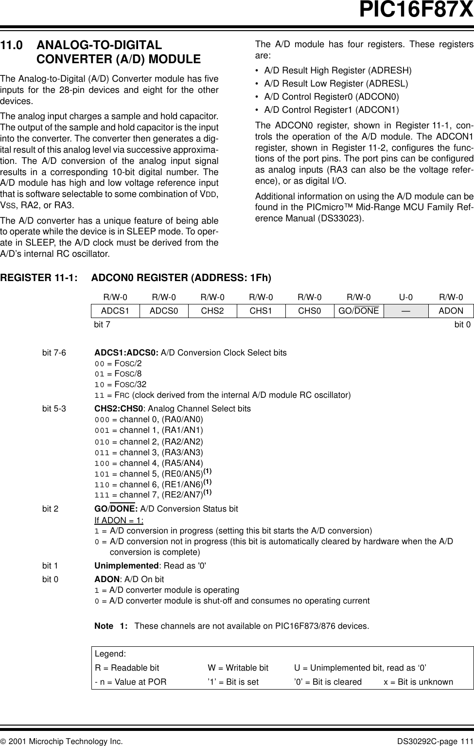
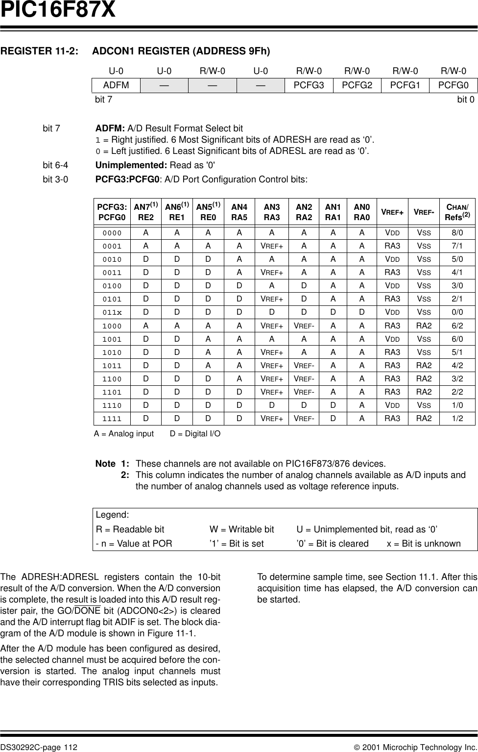
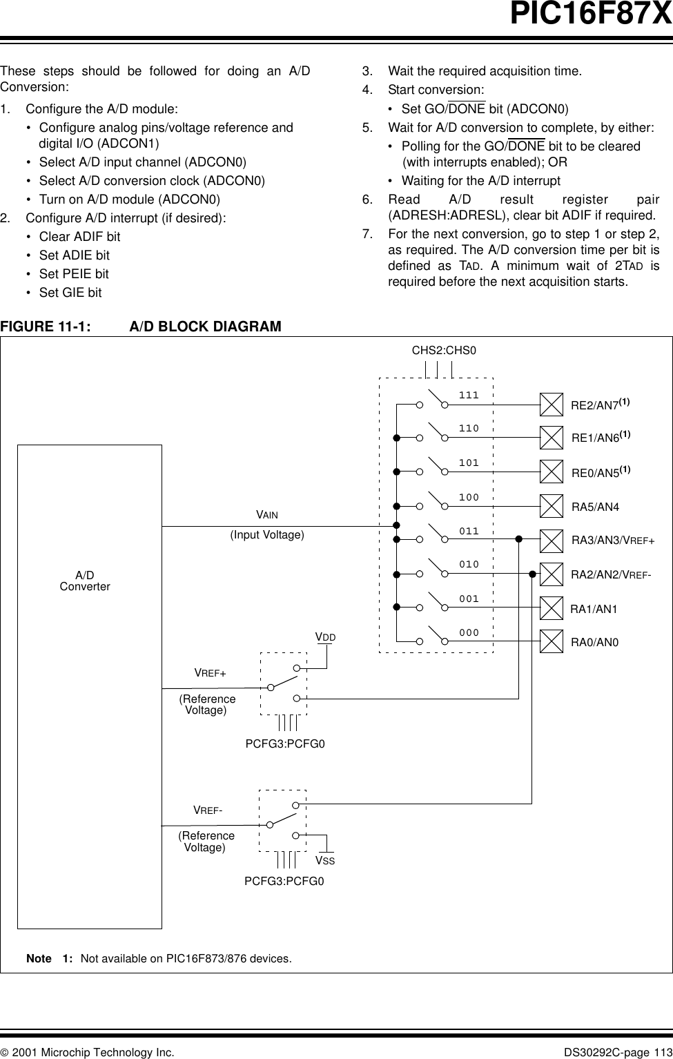
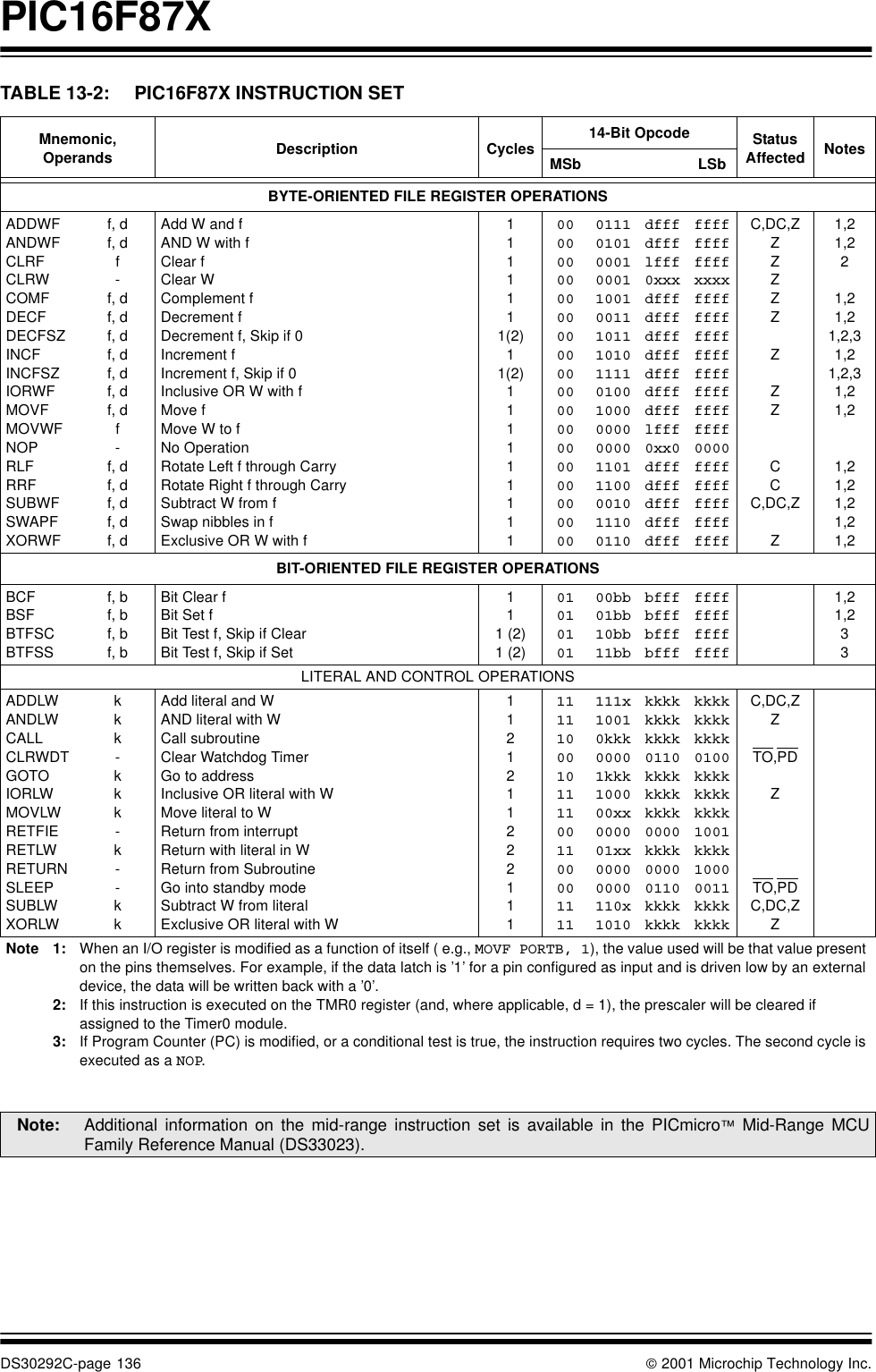
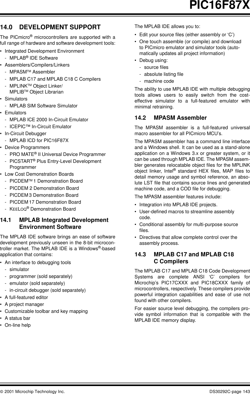
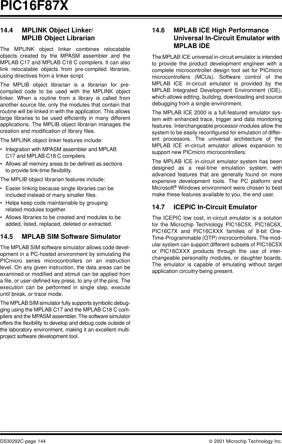
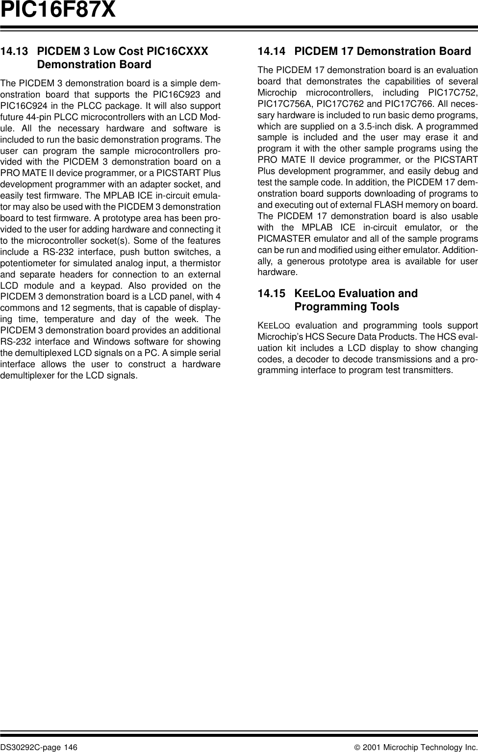
Leidos 418M1 RTR-4 Wireless Option User Manual PIC16F87X Data Sheet

Science Application International Corporation RTR-4 Wireless Option PIC16F87X Data Sheet

manual pic 16f877
 2001 Microchip Technology Inc.  DS30292CPIC16F87XData Sheet28/40-Pin 8-Bit CMOS FLASHMicrocontrollers
DS30292C - page ii  2001 Microchip Technology Inc.“All rights reserved. Copyright © 2001, Microchip TechnologyIncorporated, USA. Information contained in this publicationregarding device applications and the like is intended throughsuggestion only and may be superseded by updates. No rep-resentation or warranty is given and no liability is assumed byMicrochip Technology Incorporated with respect to the accu-racy or use of such information, or infringement of patents orother intellectual property rights arising from such use or oth-erwise. Use of Microchip’s products as critical components inlife support systems is not authorized except with expresswritten approval by Microchip. No licenses are conveyed,implicitly or otherwise, under any intellectual property rights.The Microchip logo and name are registered trademarks ofMicrochip Technology Inc. in the U.S.A. and other countries.All rights reserved. All other trademarks mentioned herein arethe property of their respective companies. No licenses areconveyed, implicitly or otherwise, under any intellectual prop-erty rights.”TrademarksThe Microchip name, logo, PIC, PICmicro, PICMASTER, PIC-START, PRO MATE, KEELOQ, SEEVAL, MPLAB and TheEmbedded Control Solutions Company are registered trade-marks of Microchip Technology Incorporated in the U.S.A. andother countries.Total Endurance, ICSP, In-Circuit Serial Programming, Filter-Lab, MXDEV, microID, FlexROM,  fuzzyLAB, MPASM,MPLINK, MPLIB, PICDEM, ICEPIC, Migratable Memory,FanSense, ECONOMONITOR and SelectMode are trade-marks of Microchip Technology Incorporated in the U.S.A.Serialized Quick Term Programming (SQTP) is a service markof Microchip Technology Incorporated in the U.S.A.All other trademarks mentioned herein are property of theirrespective companies.© 2001, Microchip Technology Incorporated, Printed in theU.S.A., All Rights Reserved.Microchip received QS-9000 quality system certification for its worldwide headquarters, design and wafer fabrication facilities in Chandler and Tempe, Arizona in July 1999. The Company’s quality system processes and procedures are QS-9000 compliant for its PICmicro® 8-bit MCUs, KEELOQ® code hopping devices, Serial EEPROMs and microperipheral products. In addition, Microchip’s quality system for the design and manufacture of development systems is ISO 9001 certified.
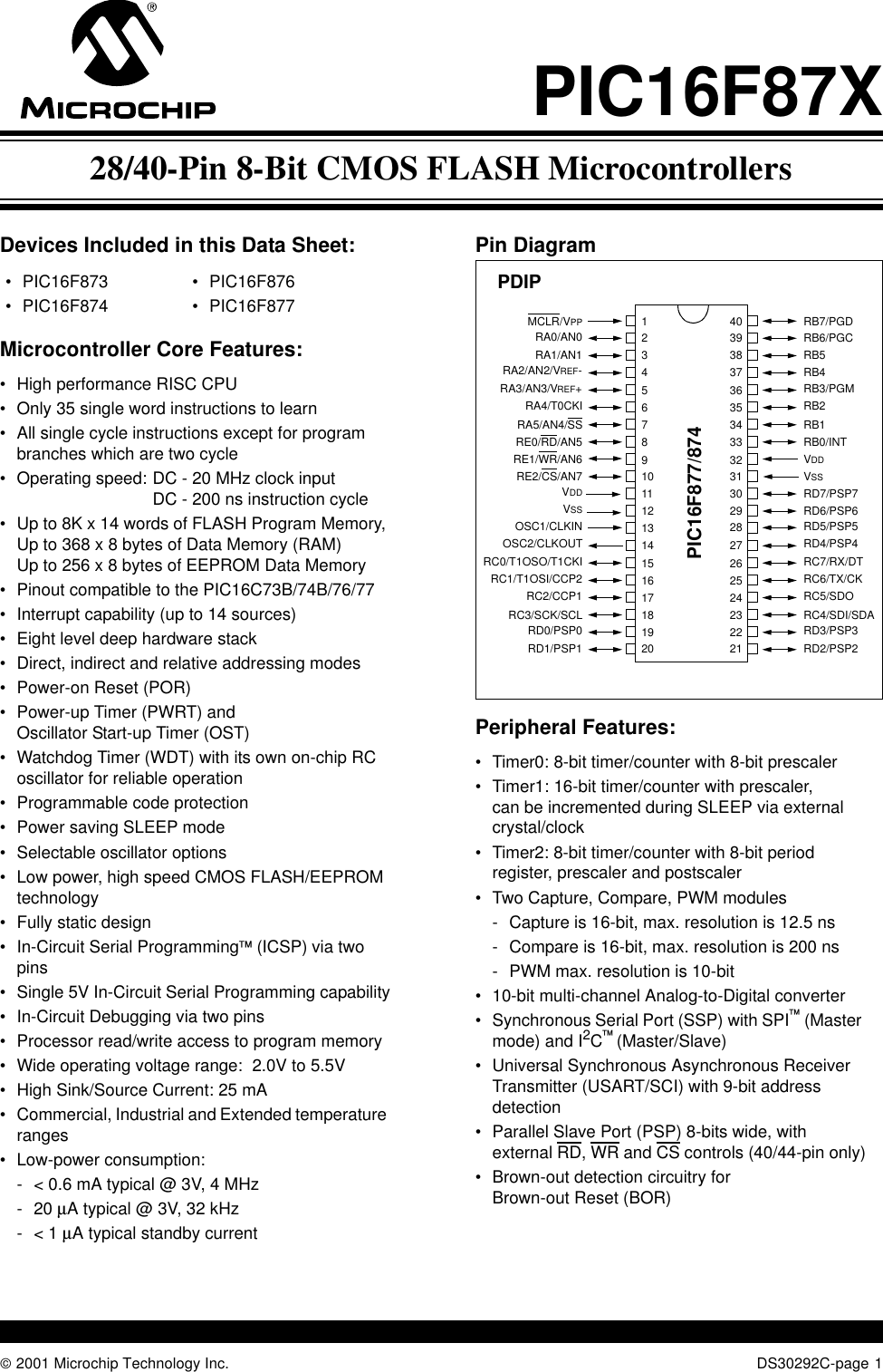
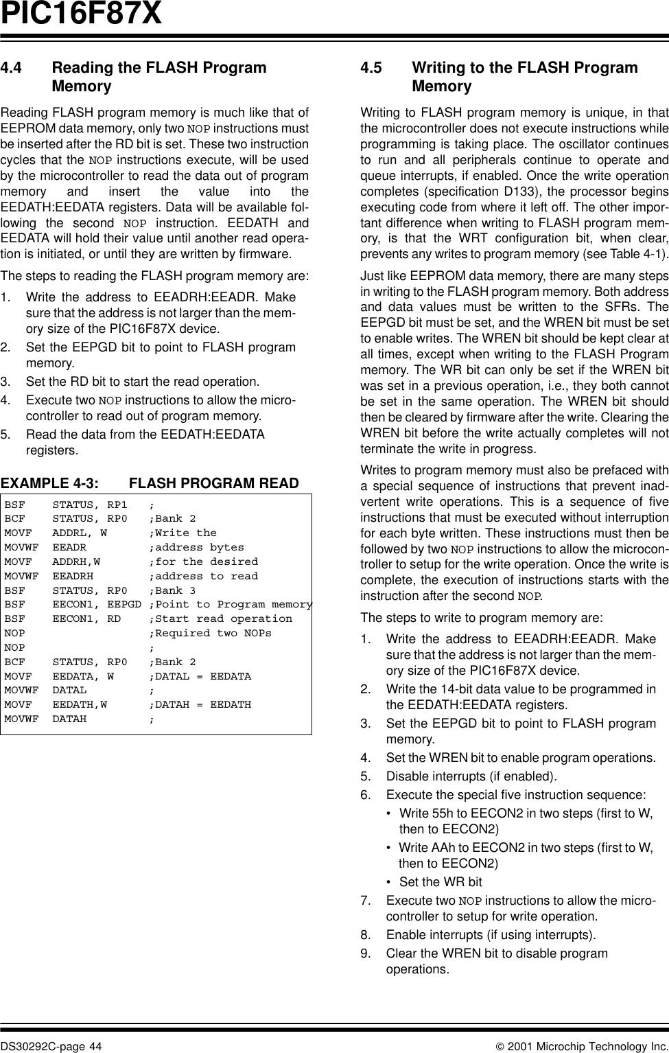
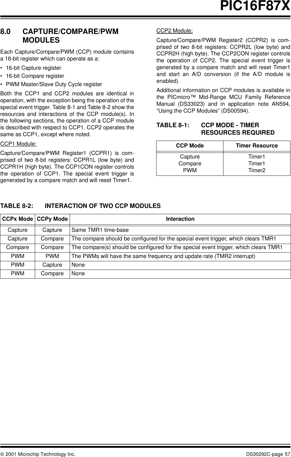
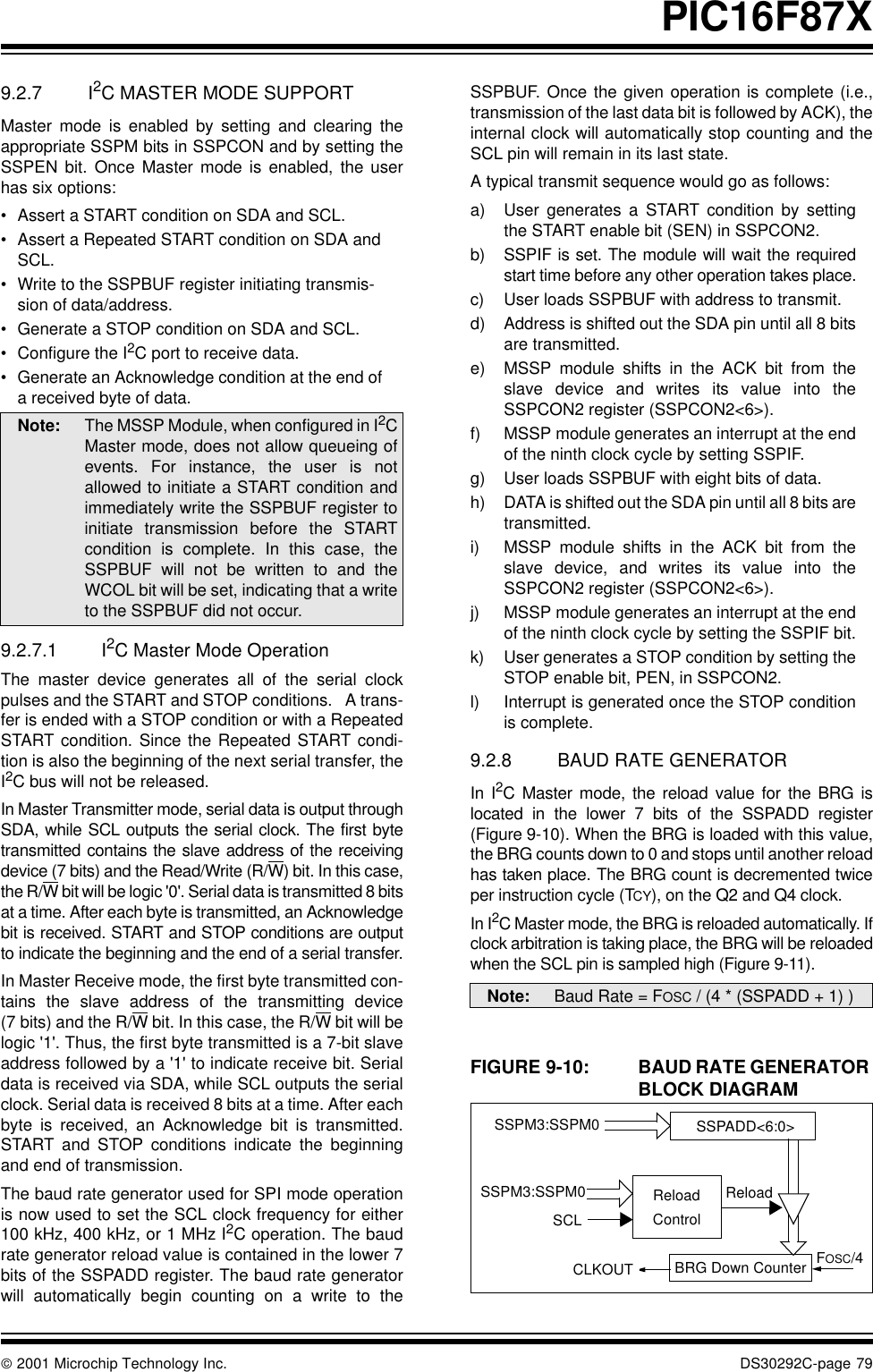
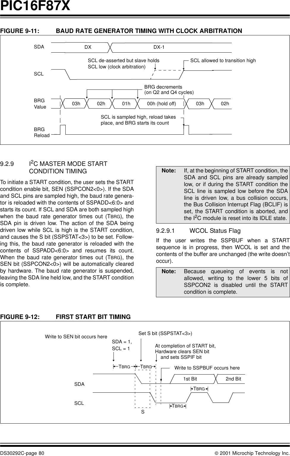
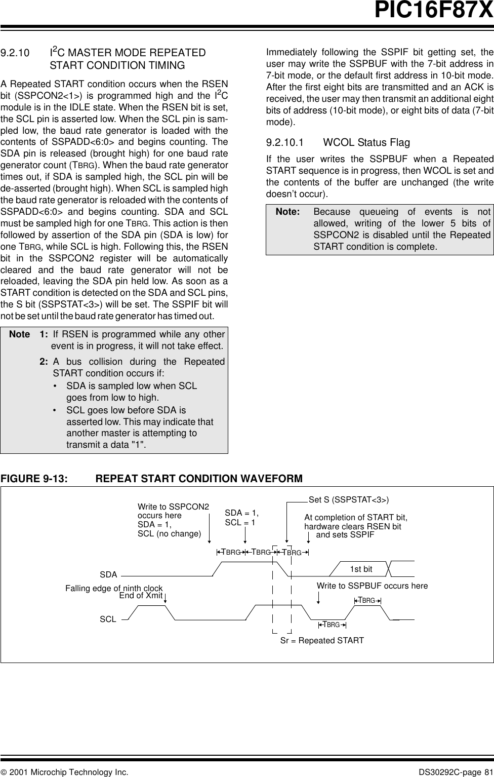
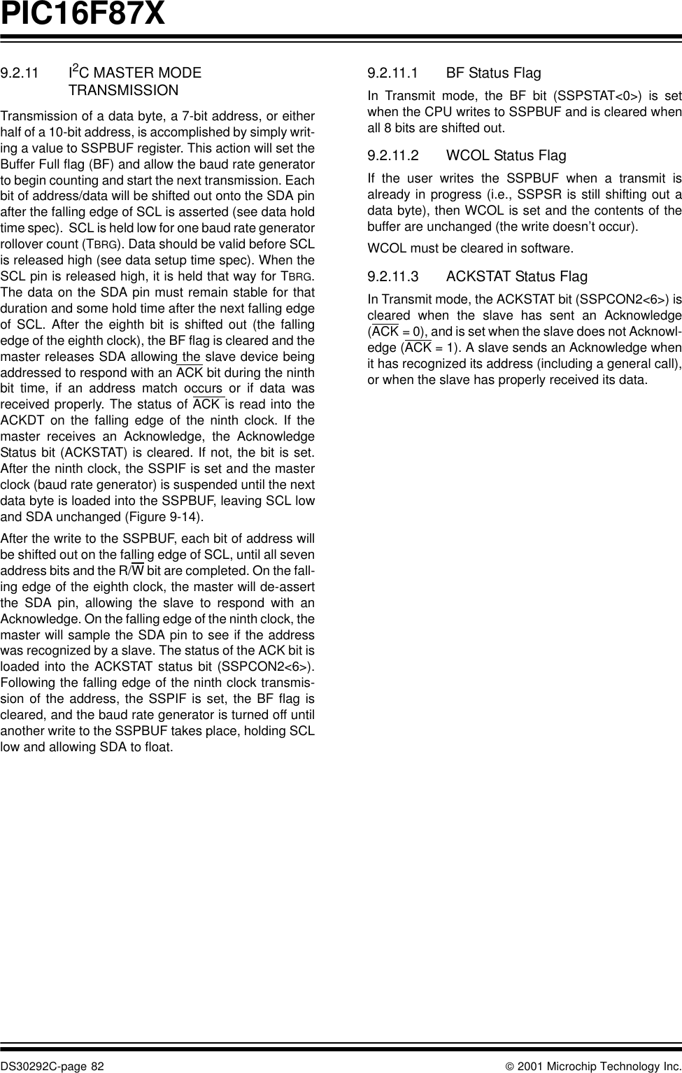
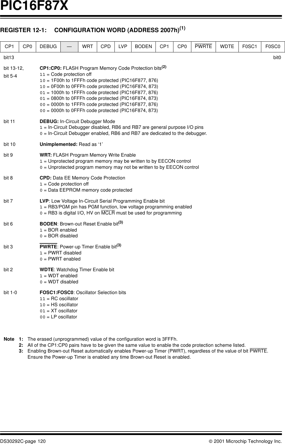
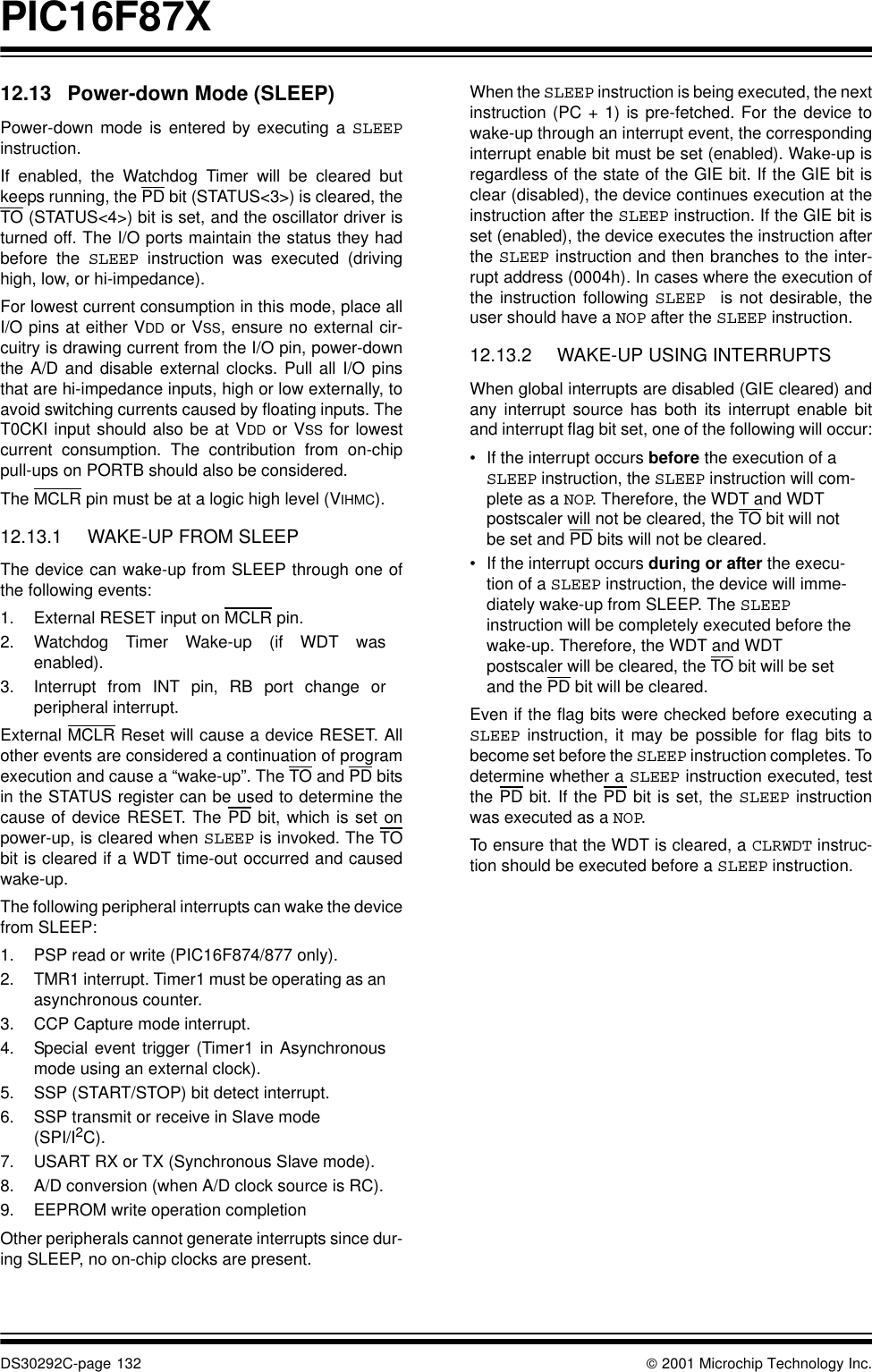
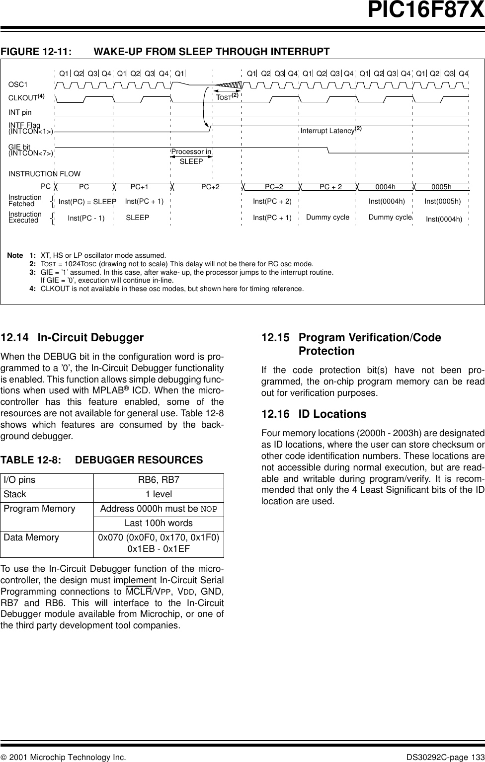
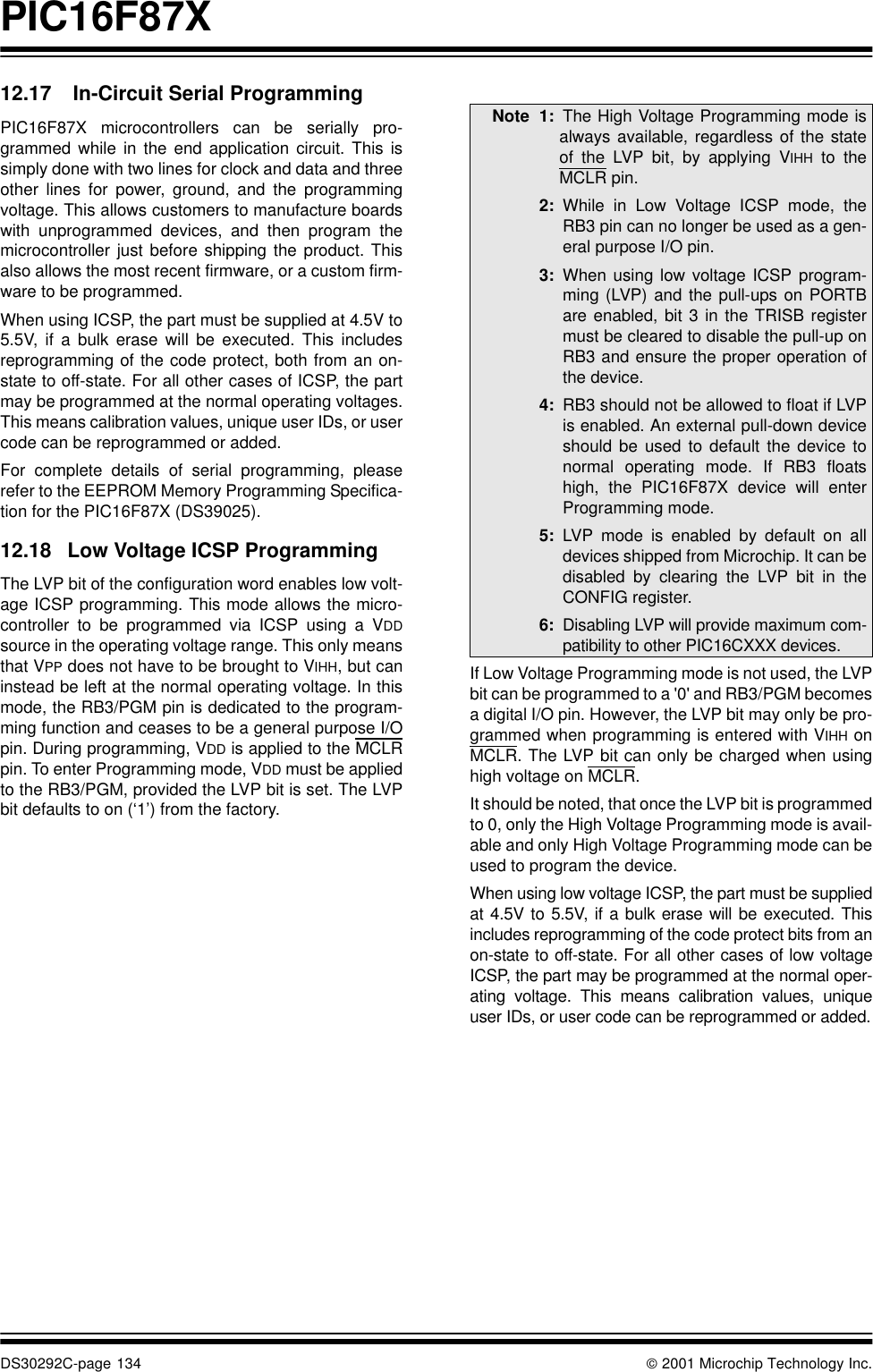
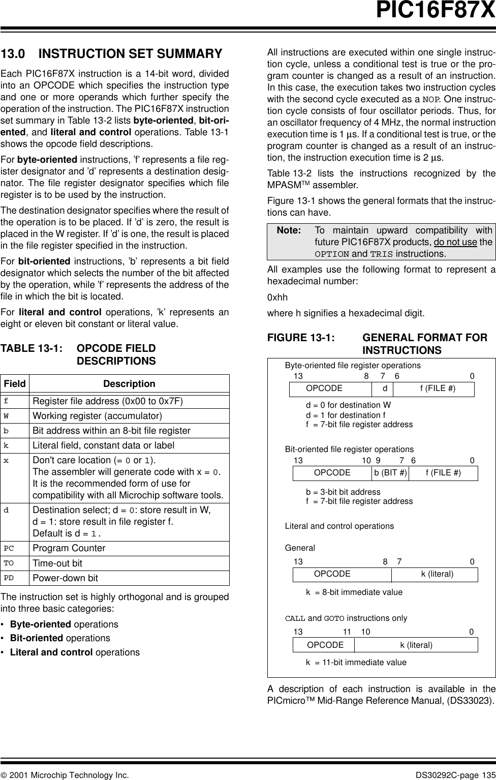
 2001 Microchip Technology Inc. DS30292C-page 1PIC16F87XDevices Included in this Data Sheet:Microcontroller Core Features:•High performance RISC CPU•Only 35 single word instructions to learn•All single cycle instructions except for program branches which are two cycle•Operating speed: DC - 20 MHz clock inputDC - 200 ns instruction cycle•Up to 8K x 14 words of FLASH Program Memory, Up to 368 x 8 bytes of Data Memory (RAM)Up to 256 x 8 bytes of EEPROM Data Memory•Pinout compatible to the PIC16C73B/74B/76/77•Interrupt capability (up to 14 sources)•Eight level deep hardware stack•Direct, indirect and relative addressing modes•Power-on Reset (POR)•Power-up Timer (PWRT) andOscillator Start-up Timer (OST) •Watchdog Timer (WDT) with its own on-chip RC oscillator for reliable operation•Programmable code protection•Power saving SLEEP mode•Selectable oscillator options•Low power, high speed CMOS FLASH/EEPROM technology•Fully static design•In-Circuit Serial Programming (ICSP) via two pins•Single 5V In-Circuit Serial Programming capability•In-Circuit Debugging via two pins•Processor read/write access to program memory•Wide operating voltage range:  2.0V to 5.5V•High Sink/Source Current: 25 mA•Commercial, Industrial and Extended temperature ranges•Low-power consumption: - < 0.6 mA typical @ 3V, 4 MHz-20 µA typical @ 3V, 32 kHz-< 1 µA typical standby currentPin Diagram Peripheral Features:•Timer0: 8-bit timer/counter with 8-bit prescaler•Timer1: 16-bit timer/counter with prescaler,can be incremented during SLEEP via external crystal/clock•Timer2: 8-bit timer/counter with 8-bit periodregister, prescaler and postscaler •Two Capture, Compare, PWM modules- Capture is 16-bit, max. resolution is 12.5 ns- Compare is 16-bit, max. resolution is 200 ns- PWM max. resolution is 10-bit•10-bit multi-channel Analog-to-Digital converter•Synchronous Serial Port (SSP) with SPI (Master mode) and I2C (Master/Slave)•Universal Synchronous Asynchronous Receiver Transmitter (USART/SCI) with 9-bit address detection•Parallel Slave Port (PSP) 8-bits wide, withexternal RD, WR and CS controls (40/44-pin only)•Brown-out detection circuitry forBrown-out Reset (BOR)•PIC16F873•PIC16F874•PIC16F876•PIC16F877 RB7/PGDRB6/PGCRB5RB4RB3/PGMRB2RB1RB0/INTVDDVSSRD7/PSP7RD6/PSP6RD5/PSP5RD4/PSP4RC7/RX/DTRC6/TX/CKRC5/SDORC4/SDI/SDARD3/PSP3RD2/PSP2MCLR/VPPRA0/AN0RA1/AN1RA2/AN2/VREF-RA3/AN3/VREF+RA4/T0CKIRA5/AN4/SSRE0/RD/AN5RE1/WR/AN6RE2/CS/AN7VDDVSSOSC1/CLKINOSC2/CLKOUTRC0/T1OSO/T1CKIRC1/T1OSI/CCP2RC2/CCP1RC3/SCK/SCLRD0/PSP0RD1/PSP112345678910111213141516171819204039383736353433323130292827262524232221PIC16F877/874PDIP28/40-Pin 8-Bit CMOS FLASH Microcontrollers
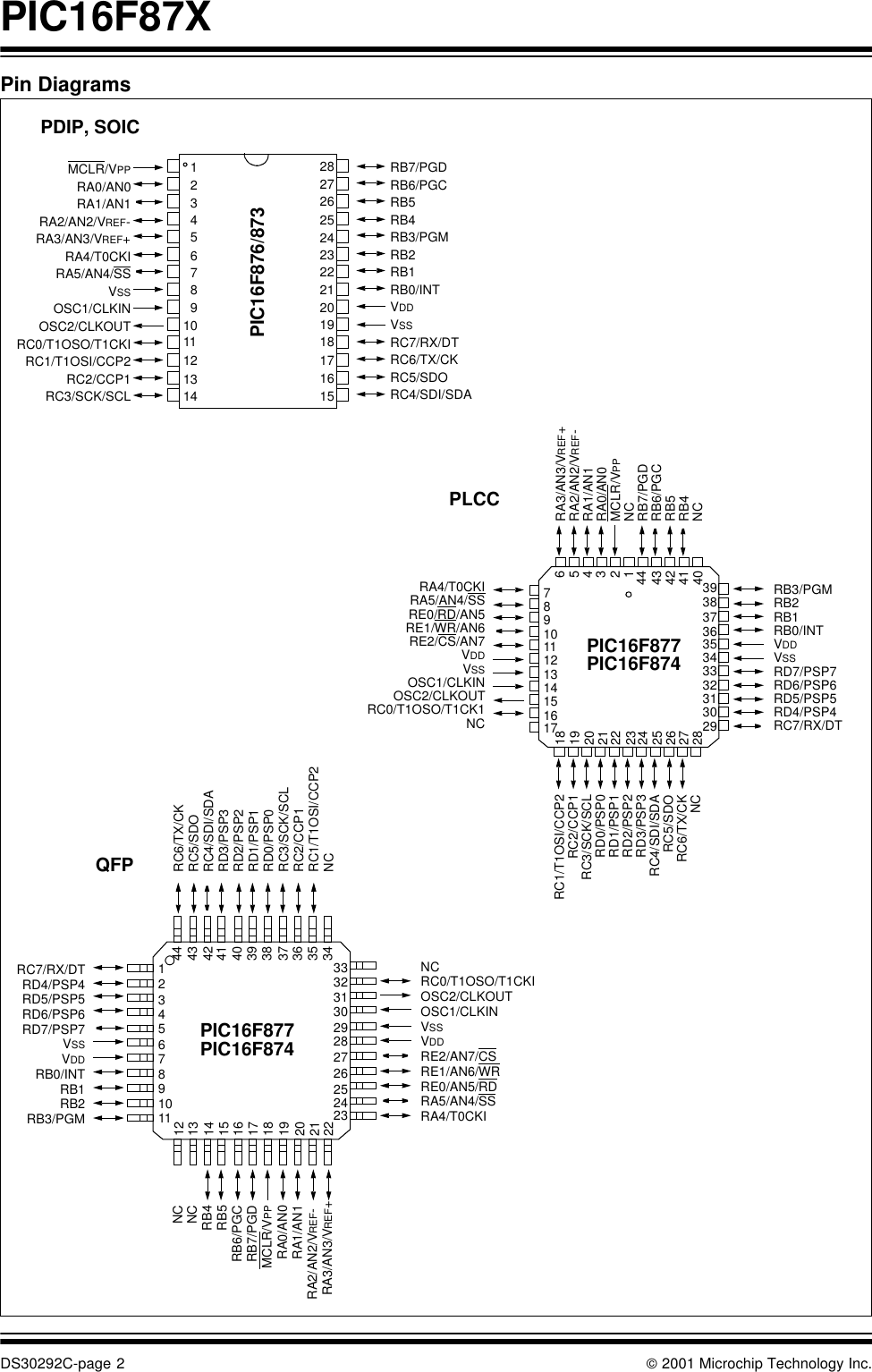
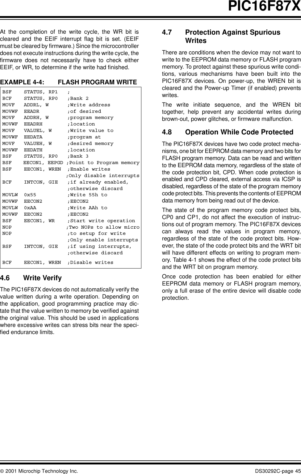
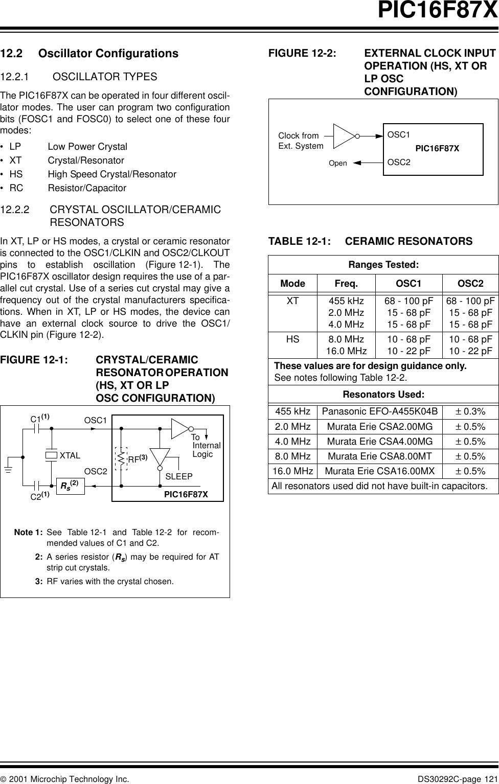
PIC16F87XDS30292C-page 2  2001 Microchip Technology Inc.Pin DiagramsPIC16F876/8731011234561879121314 1516171819202324252627282221MCLR/VPPRA0/AN0RA1/AN1RA2/AN2/VREF-RA3/AN3/VREF+RA4/T0CKIRA5/AN4/SSVSSOSC1/CLKINOSC2/CLKOUTRC0/T1OSO/T1CKIRC1/T1OSI/CCP2RC2/CCP1RC3/SCK/SCLRB7/PGDRB6/PGCRB5RB4RB3/PGMRB2RB1RB0/INTVDDVSSRC7/RX/DTRC6/TX/CKRC5/SDORC4/SDI/SDA1011121314151617181920212223242526448765432127282930313233343536373839404142439PIC16F877RA4/T0CKIRA5/AN4/SSRE0/RD/AN5OSC1/CLKINOSC2/CLKOUTRC0/T1OSO/T1CK1NCRE1/WR/AN6RE2/CS/AN7VDDVSSRB3/PGMRB2RB1RB0/INTVDDVSSRD7/PSP7RD6/PSP6RD5/PSP5RD4/PSP4RC7/RX/DTRA3/AN3/VREF+RA2/AN2/VREF-RA1/AN1RA0/AN0MCLR/VPPNCRB7/PGDRB6/PGCRB5RB4NCNCRC6/TX/CKRC5/SDORC4/SDI/SDARD3/PSP3RD2/PSP2RD1/PSP1RD0/PSP0RC3/SCK/SCLRC2/CCP1RC1/T1OSI/CCP210112345611819202122121314153887444342414039161729303132332324252627283634359PIC16F87737RA3/AN3/VREF+RA2/AN2/VREF-RA1/AN1RA0/AN0MCLR/VPPNCRB7/PGDRB6/PGCRB5RB4NC RC6/TX/CKRC5/SDORC4/SDI/SDARD3/PSP3RD2/PSP2RD1/PSP1RD0/PSP0RC3/SCK/SCLRC2/CCP1RC1/T1OSI/CCP2NCNCRC0/T1OSO/T1CKIOSC2/CLKOUTOSC1/CLKINVSSVDDRE2/AN7/CSRE1/AN6/WRRE0/AN5/RDRA5/AN4/SSRA4/T0CKIRC7/RX/DTRD4/PSP4RD5/PSP5RD6/PSP6RD7/PSP7VSSVDDRB0/INTRB1RB2RB3/PGMPLCCQFPPDIP, SOICPIC16F874PIC16F874
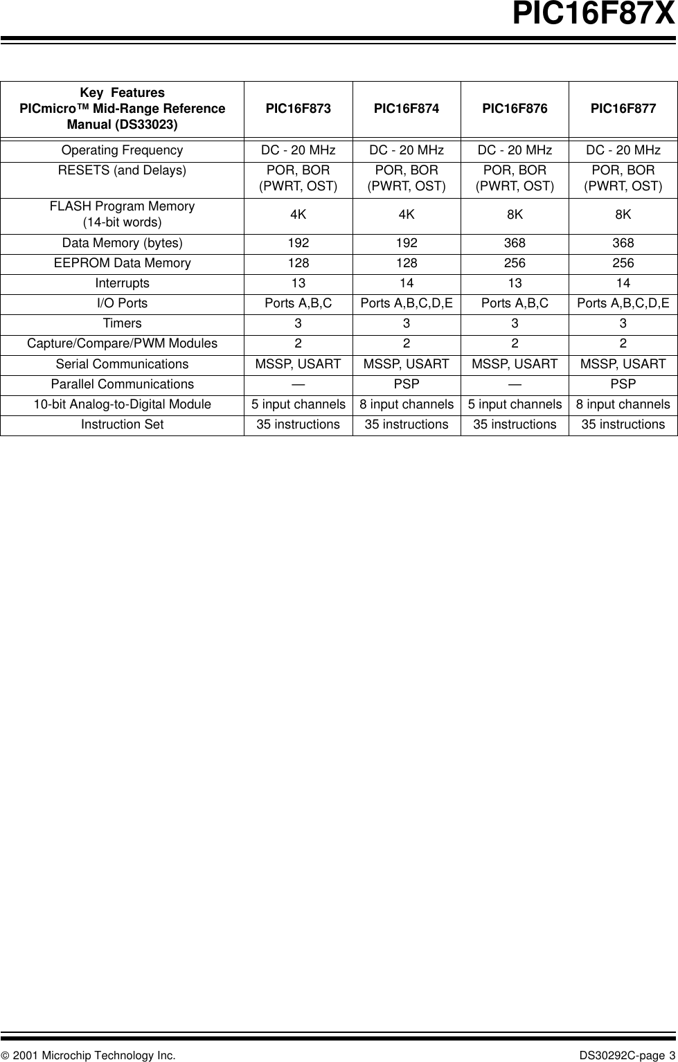
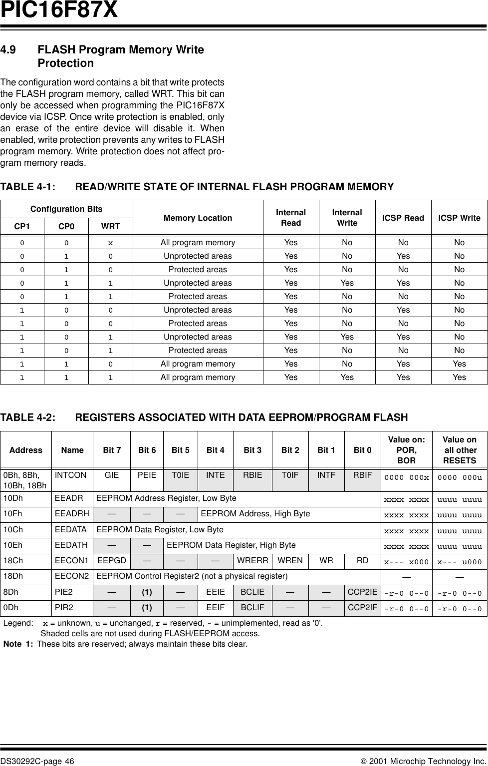
 2001 Microchip Technology Inc. DS30292C-page 3PIC16F87XKey  FeaturesPICmicro™ Mid-Range Reference Manual (DS33023) PIC16F873 PIC16F874 PIC16F876 PIC16F877Operating Frequency DC - 20 MHz DC - 20 MHz DC - 20 MHz DC - 20 MHzRESETS (and Delays) POR, BOR (PWRT, OST) POR, BOR (PWRT, OST) POR, BOR (PWRT, OST) POR, BOR (PWRT, OST)FLASH Program Memory (14-bit words) 4K 4K 8K 8KData Memory (bytes) 192 192 368 368EEPROM Data Memory 128 128 256 256Interrupts 13 14 13 14I/O Ports Ports A,B,C Ports A,B,C,D,E Ports A,B,C Ports A,B,C,D,ETimers 3333Capture/Compare/PWM Modules 2 2 2 2Serial Communications MSSP, USART MSSP, USART MSSP, USART MSSP, USARTParallel Communications —PSP —PSP10-bit Analog-to-Digital Module 5 input channels 8 input channels 5 input channels 8 input channelsInstruction Set 35 instructions 35 instructions 35 instructions 35 instructions
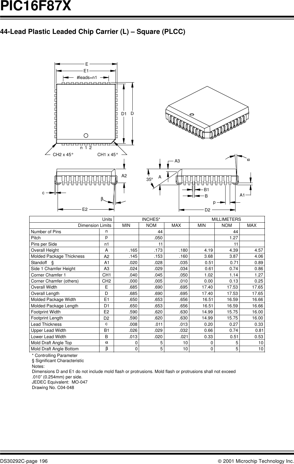
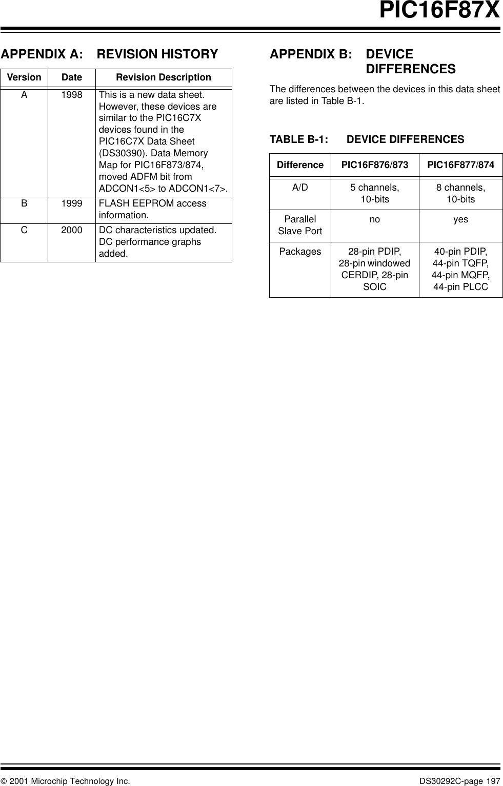
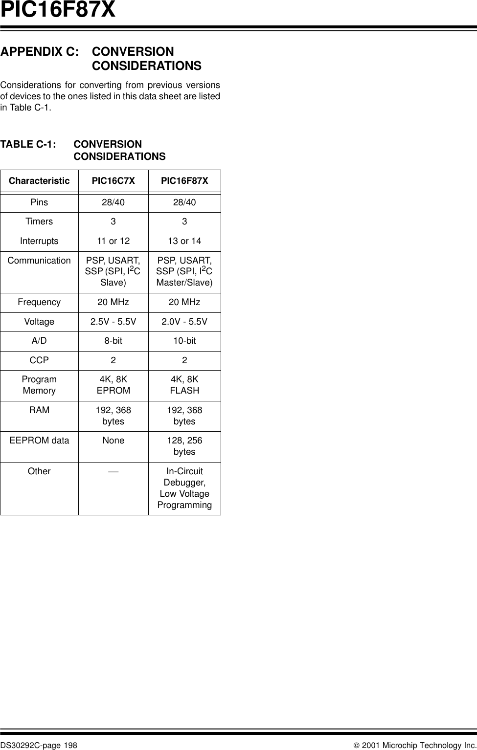
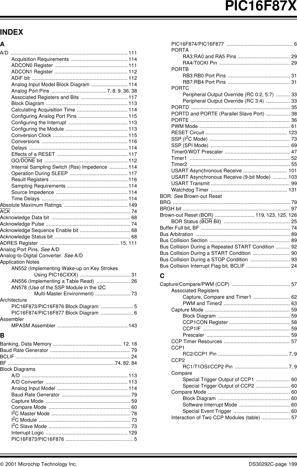
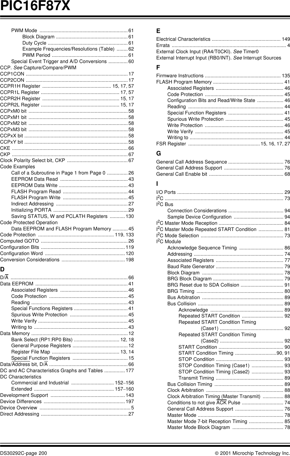
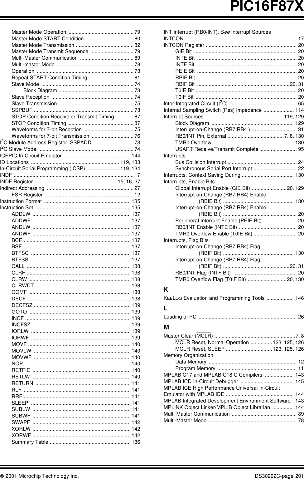
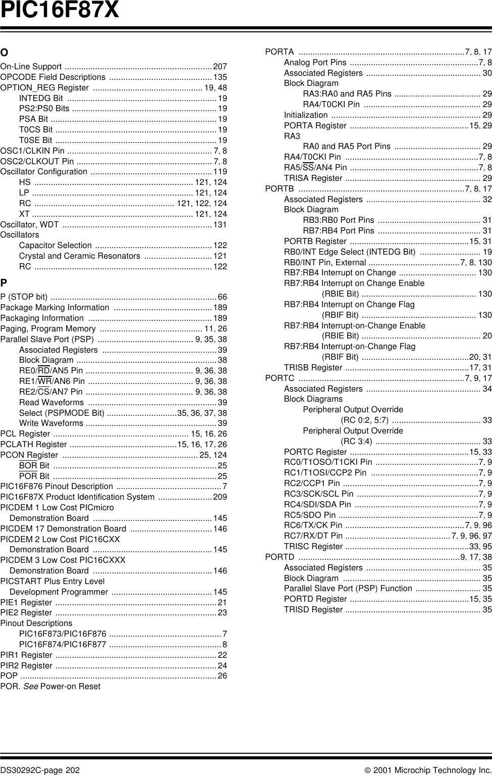
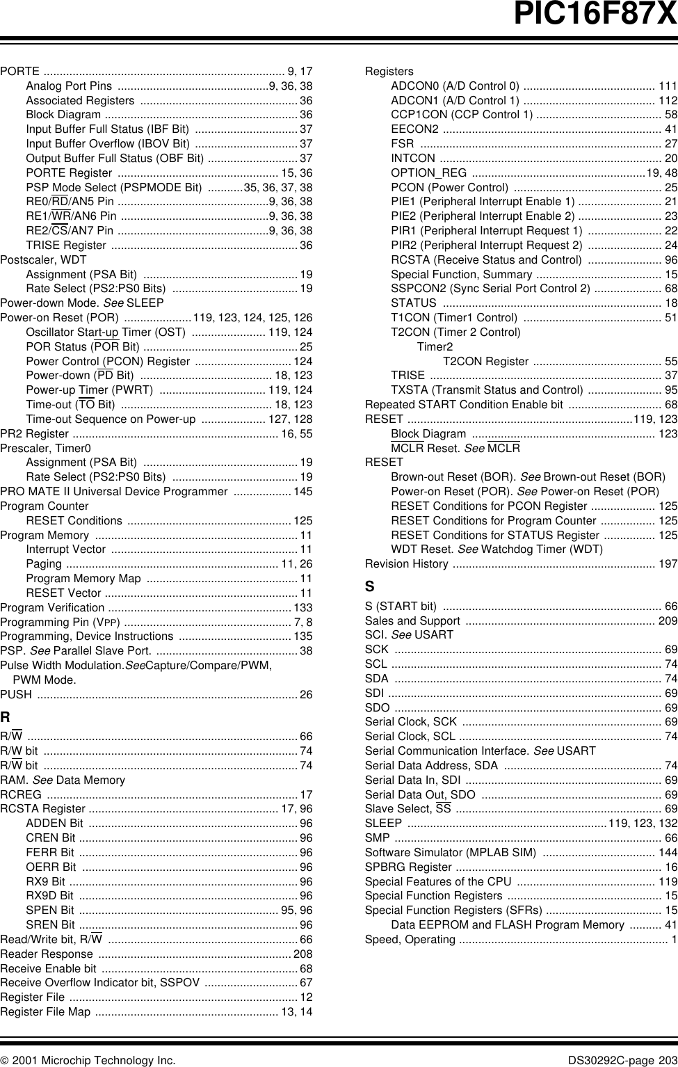
PIC16F87XDS30292C-page 4  2001 Microchip Technology Inc.Table of Contents1.0 Device Overview ................................................................................................................................................... 52.0 Memory Organization.......................................................................................................................................... 113.0 I/O Ports.............................................................................................................................................................. 294.0 Data EEPROM and FLASH Program Memory.................................................................................................... 415.0 Timer0 Module .................................................................................................................................................... 476.0 Timer1 Module .................................................................................................................................................... 517.0 Timer2 Module .................................................................................................................................................... 558.0 Capture/Compare/PWM Modules....................................................................................................................... 579.0 Master Synchronous Serial Port (MSSP) Module............................................................................................... 6510.0 Addressable Universal Synchronous Asynchronous Receiver Transmitter (USART) ........................................ 9511.0 Analog-to-Digital Converter (A/D) Module......................................................................................................... 11112.0 Special Features of the CPU............................................................................................................................. 11913.0 Instruction Set Summary................................................................................................................................... 13514.0 Development Support ....................................................................................................................................... 14315.0 Electrical Characteristics................................................................................................................................... 14916.0 DC and AC Characteristics Graphs and Tables................................................................................................ 17717.0 Packaging Information ...................................................................................................................................... 189Appendix A: Revision History .................................................................................................................................... 197Appendix B: Device Differences ................................................................................................................................ 197Appendix C: Conversion Considerations ................................................................................................................... 198Index .......................................................................................................................................................................... 199On-Line Support......................................................................................................................................................... 207Reader Response ...................................................................................................................................................... 208PIC16F87X Product Identification System ................................................................................................................. 209TO OUR VALUED CUSTOMERSIt is our intention to provide our valued customers with the best documentation possible to ensure successful use of your Microchipproducts. To this end, we will continue to improve our publications to better suit your needs. Our publications will be refined andenhanced as new volumes and updates are introduced. If you have any questions or comments regarding this publication, please contact the Marketing Communications Department viaE-mail at docerrors@mail.microchip.com or fax the Reader Response Form in the back of this data sheet to (480) 792-4150.We welcome your feedback.Most Current Data SheetTo obtain the most up-to-date version of this data sheet, please register at our Worldwide Web site at:http://www.microchip.comYou can determine the version of a data sheet by examining its literature number found on the bottom outside corner of any page.The last character of the literature number is the version number, (e.g., DS30000A is version A of document DS30000).ErrataAn errata sheet, describing minor operational differences from the data sheet and recommended workarounds, may exist for currentdevices. As device/documentation issues become known to us, we will publish an errata sheet. The errata will specify the revisionof silicon and revision of document to which it applies.To determine if an errata sheet exists for a particular device, please check with one of the following:•Microchip’s Worldwide Web site; http://www.microchip.com•Your local Microchip sales office (see last page)•The Microchip Corporate Literature Center; U.S. FAX: (480) 792-7277When contacting a sales office or the literature center, please specify which device, revision of silicon and data sheet (include liter-ature number) you are using.Customer Notification SystemRegister on our web site at www.microchip.com/cn to receive the most current information on all of our products.
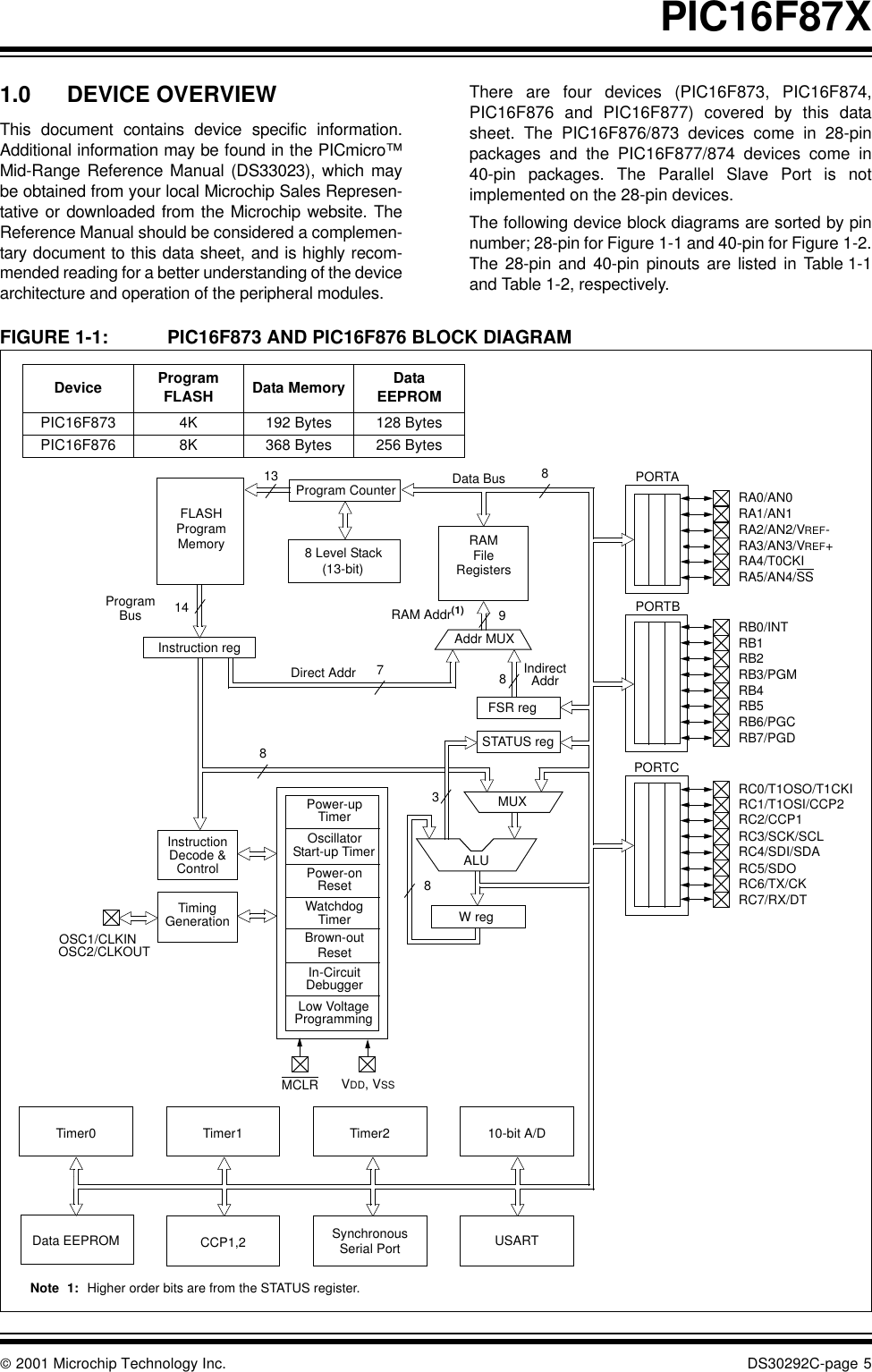
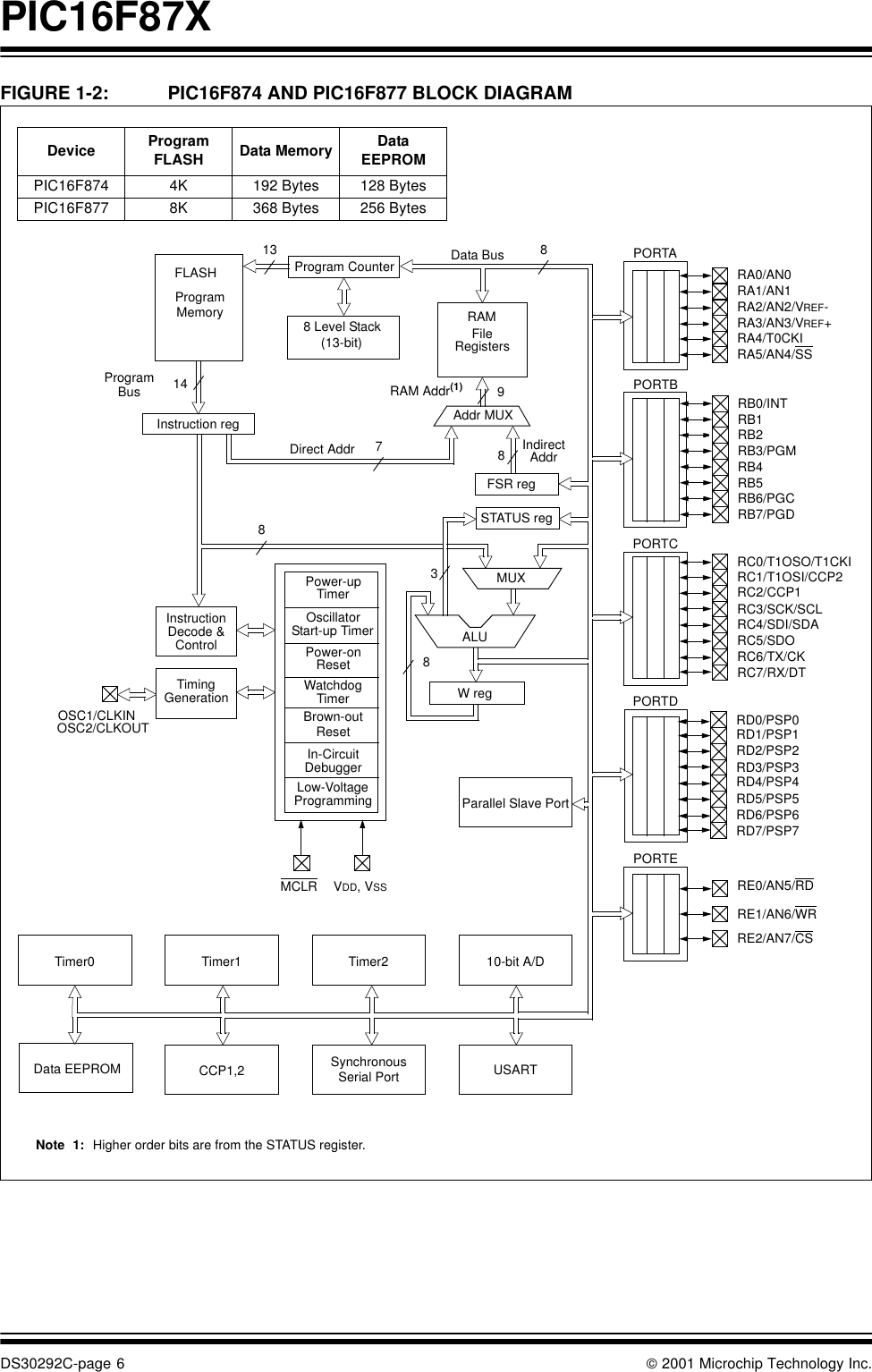
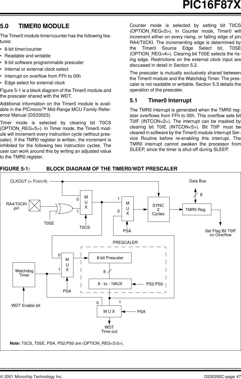
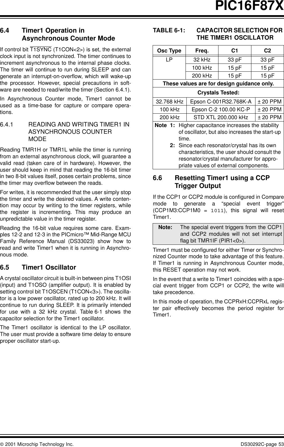
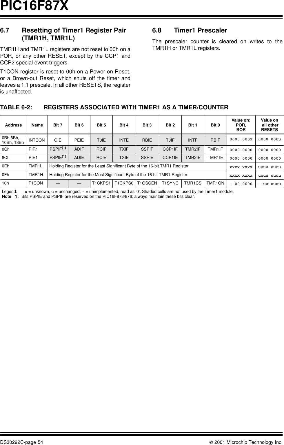
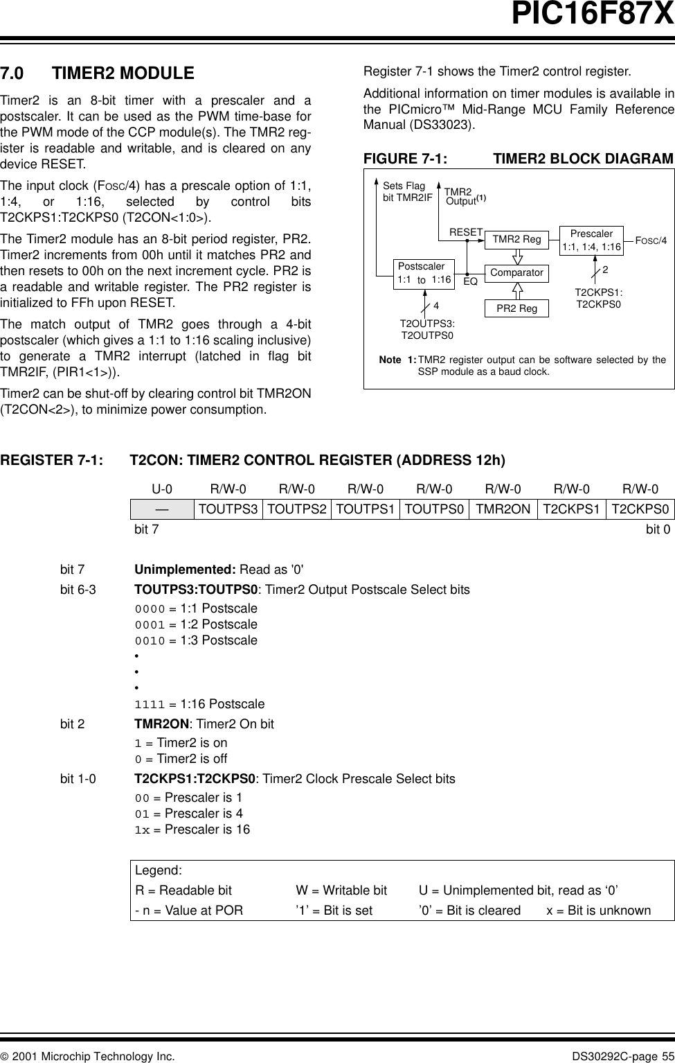
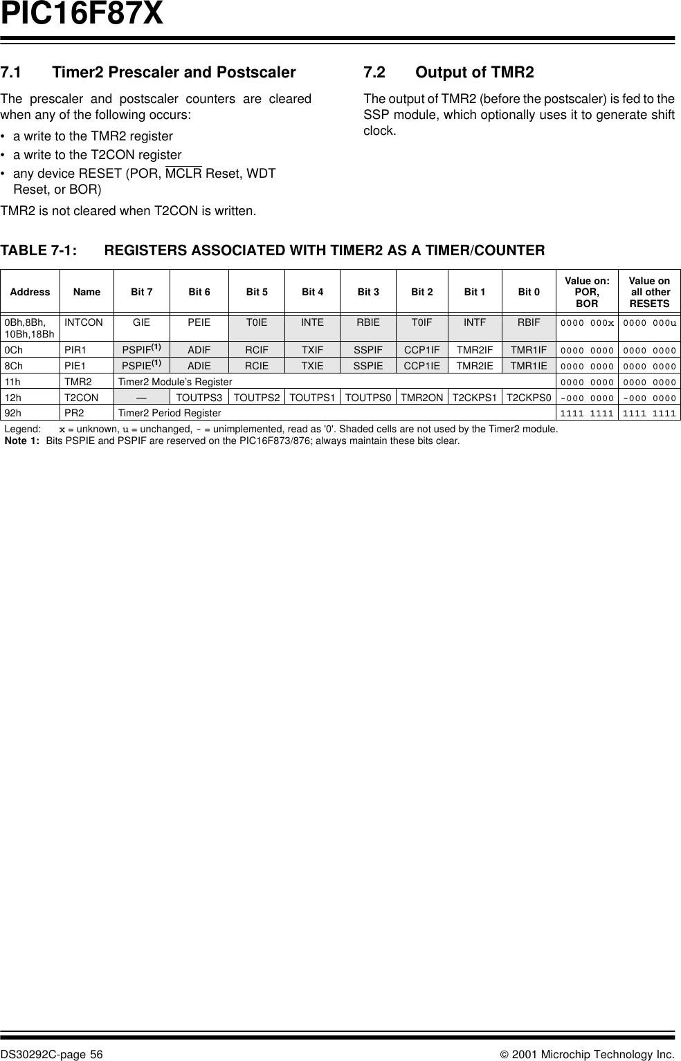
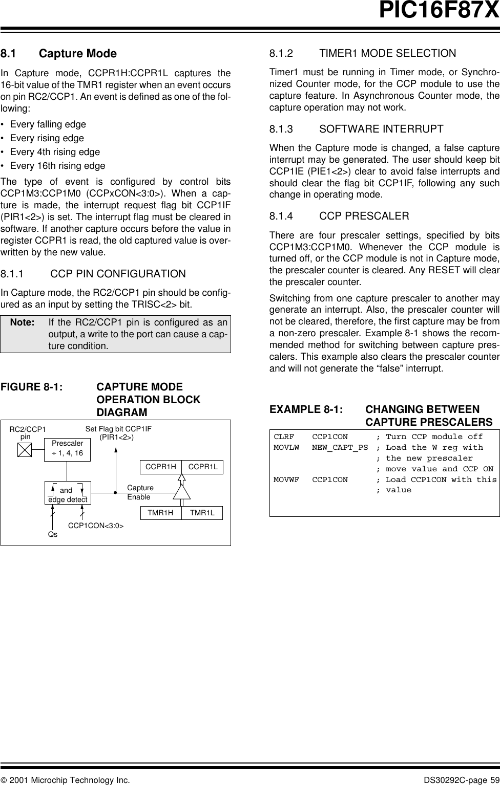
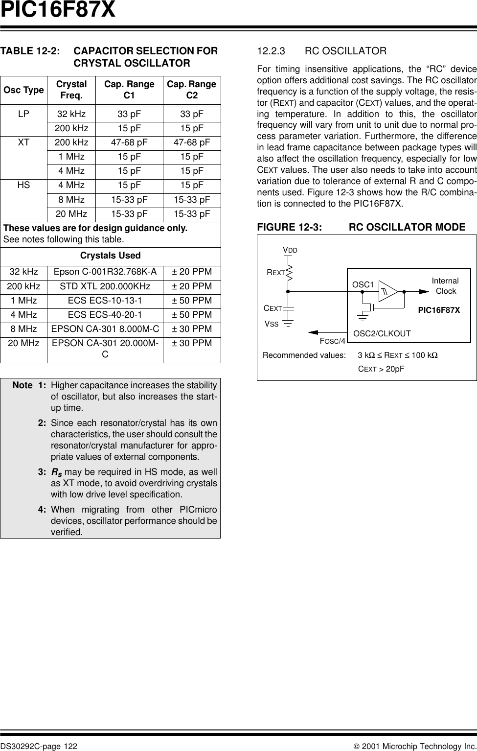
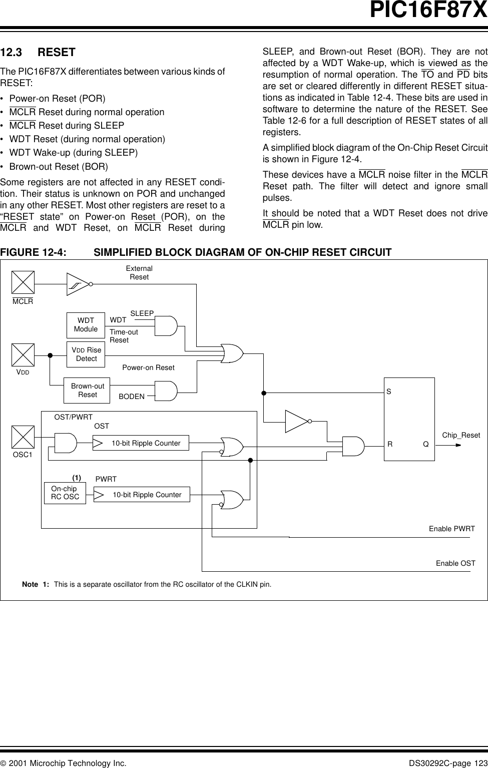
 2001 Microchip Technology Inc. DS30292C-page 5PIC16F87X1.0 DEVICE OVERVIEWThis document contains device specific information.Additional information may be found in the PICmicro™Mid-Range Reference Manual (DS33023), which maybe obtained from your local Microchip Sales Represen-tative or downloaded from the Microchip website. TheReference Manual should be considered a complemen-tary document to this data sheet, and is highly recom-mended reading for a better understanding of the devicearchitecture and operation of the peripheral modules.There are four devices (PIC16F873, PIC16F874,PIC16F876 and PIC16F877) covered by this datasheet. The PIC16F876/873 devices come in 28-pinpackages and the PIC16F877/874 devices come in40-pin packages. The Parallel Slave Port is notimplemented on the 28-pin devices.The following device block diagrams are sorted by pinnumber; 28-pin for Figure 1-1 and 40-pin for Figure 1-2.The 28-pin and 40-pin pinouts are listed in Table 1-1and Table 1-2, respectively.FIGURE 1-1: PIC16F873 AND PIC16F876 BLOCK DIAGRAMFLASHProgramMemory13 Data Bus 814ProgramBusInstruction regProgram Counter8 Level Stack(13-bit)RAMFileRegistersDirect Addr 7RAM Addr(1) 9Addr MUXIndirectAddrFSR regSTATUS regMUXALUW regPower-upTimerOscillatorStart-up TimerPower-onResetWatchdogTimerInstructionDecode &ControlTimingGenerationOSC1/CLKINOSC2/CLKOUTMCLR VDD, VSSPORTAPORTBPORTCRA4/T0CKIRA5/AN4/SSRB0/INTRC0/T1OSO/T1CKIRC1/T1OSI/CCP2RC2/CCP1RC3/SCK/SCLRC4/SDI/SDARC5/SDORC6/TX/CKRC7/RX/DT88Brown-outResetNote 1: Higher order bits are from the STATUS register.USARTCCP1,2 Synchronous10-bit A/DTimer0 Timer1 Timer2Serial PortRA3/AN3/VREF+RA2/AN2/VREF-RA1/AN1RA0/AN083Data EEPROMRB1RB2RB3/PGMRB4RB5RB6/PGCRB7/PGDDevice Program FLASH Data Memory Data EEPROMPIC16F873 4K 192 Bytes 128 BytesPIC16F876 8K 368 Bytes 256 BytesIn-CircuitDebuggerLow VoltageProgramming
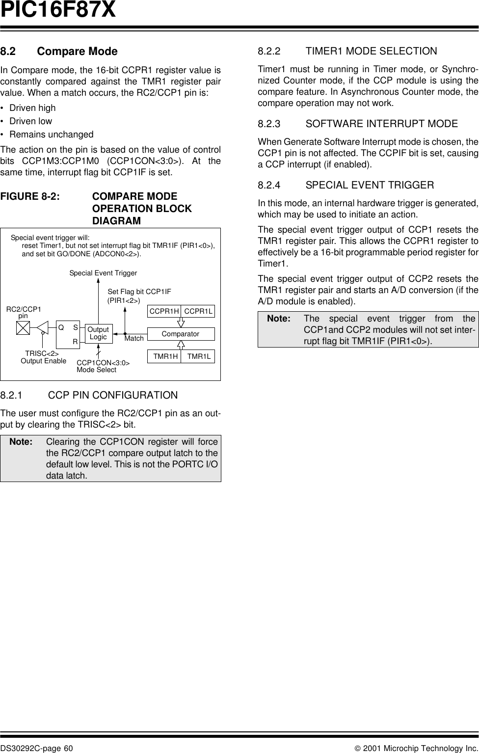
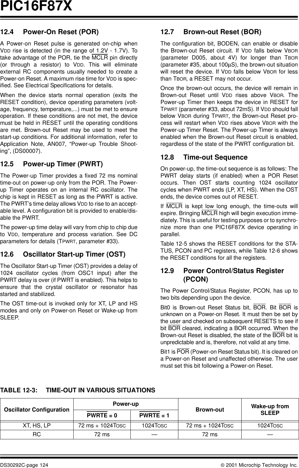
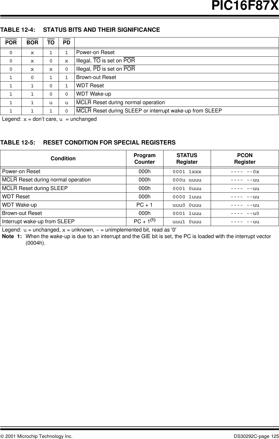
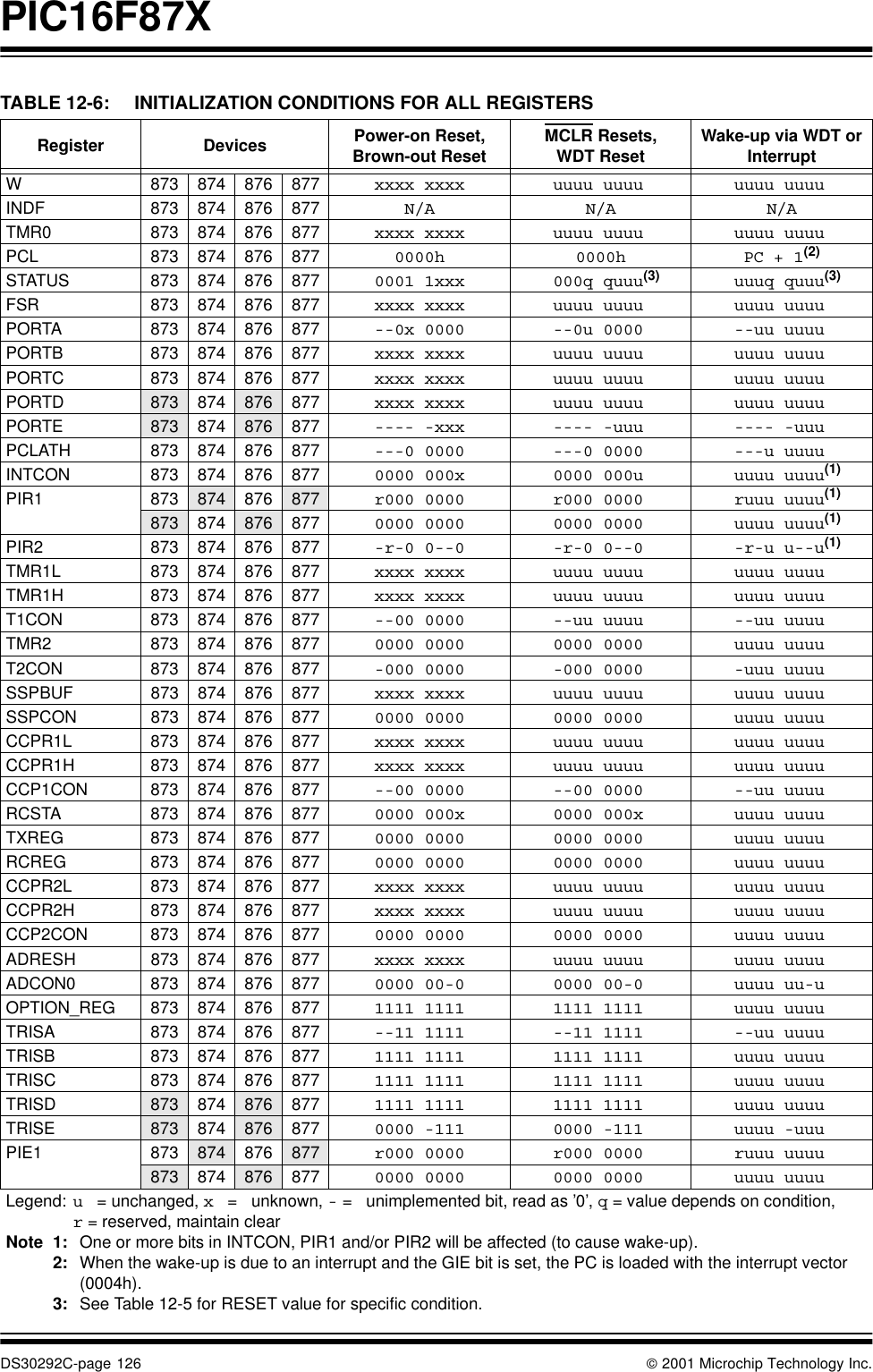
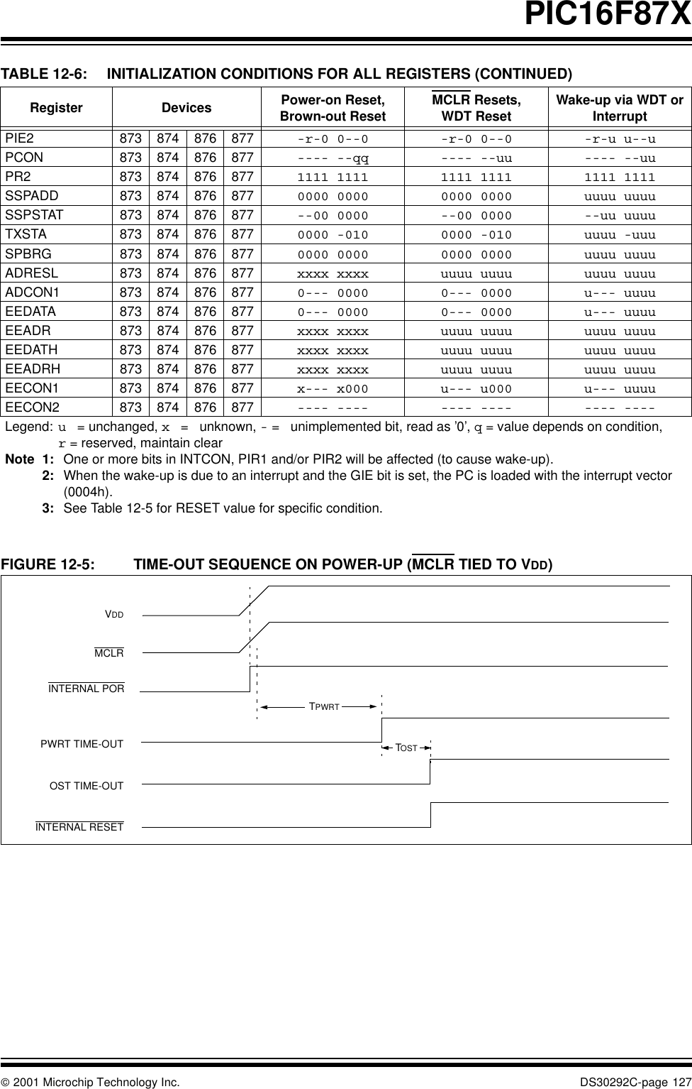
PIC16F87XDS30292C-page 6  2001 Microchip Technology Inc.FIGURE 1-2: PIC16F874 AND PIC16F877 BLOCK DIAGRAMFLASHProgramMemory13 Data Bus 814ProgramBusInstruction regProgram Counter8 Level Stack(13-bit)RAMFileRegistersDirect Addr 7RAM Addr(1) 9Addr MUXIndirectAddrFSR regSTATUS regMUXALUW regPower-upTimerOscillatorStart-up TimerPower-onResetWatchdogTimerInstructionDecode &ControlTimingGenerationOSC1/CLKINOSC2/CLKOUTMCLR VDD, VSSPORTAPORTBPORTCPORTDPORTERA4/T0CKIRA5/AN4/SSRC0/T1OSO/T1CKIRC1/T1OSI/CCP2RC2/CCP1RC3/SCK/SCLRC4/SDI/SDARC5/SDORC6/TX/CKRC7/RX/DTRE0/AN5/RDRE1/AN6/WRRE2/AN7/CS88Brown-outResetNote 1: Higher order bits are from the STATUS register.USARTCCP1,2 Synchronous10-bit A/DTimer0 Timer1 Timer2Serial PortRA3/AN3/VREF+RA2/AN2/VREF-RA1/AN1RA0/AN0Parallel Slave Port83Data EEPROMRB0/INTRB1RB2RB3/PGMRB4RB5RB6/PGCRB7/PGDDevice Program FLASH Data Memory Data EEPROMPIC16F874 4K 192 Bytes 128 BytesPIC16F877 8K 368 Bytes 256 BytesIn-CircuitDebuggerLow-VoltageProgrammingRD0/PSP0RD1/PSP1RD2/PSP2RD3/PSP3RD4/PSP4RD5/PSP5RD6/PSP6RD7/PSP7
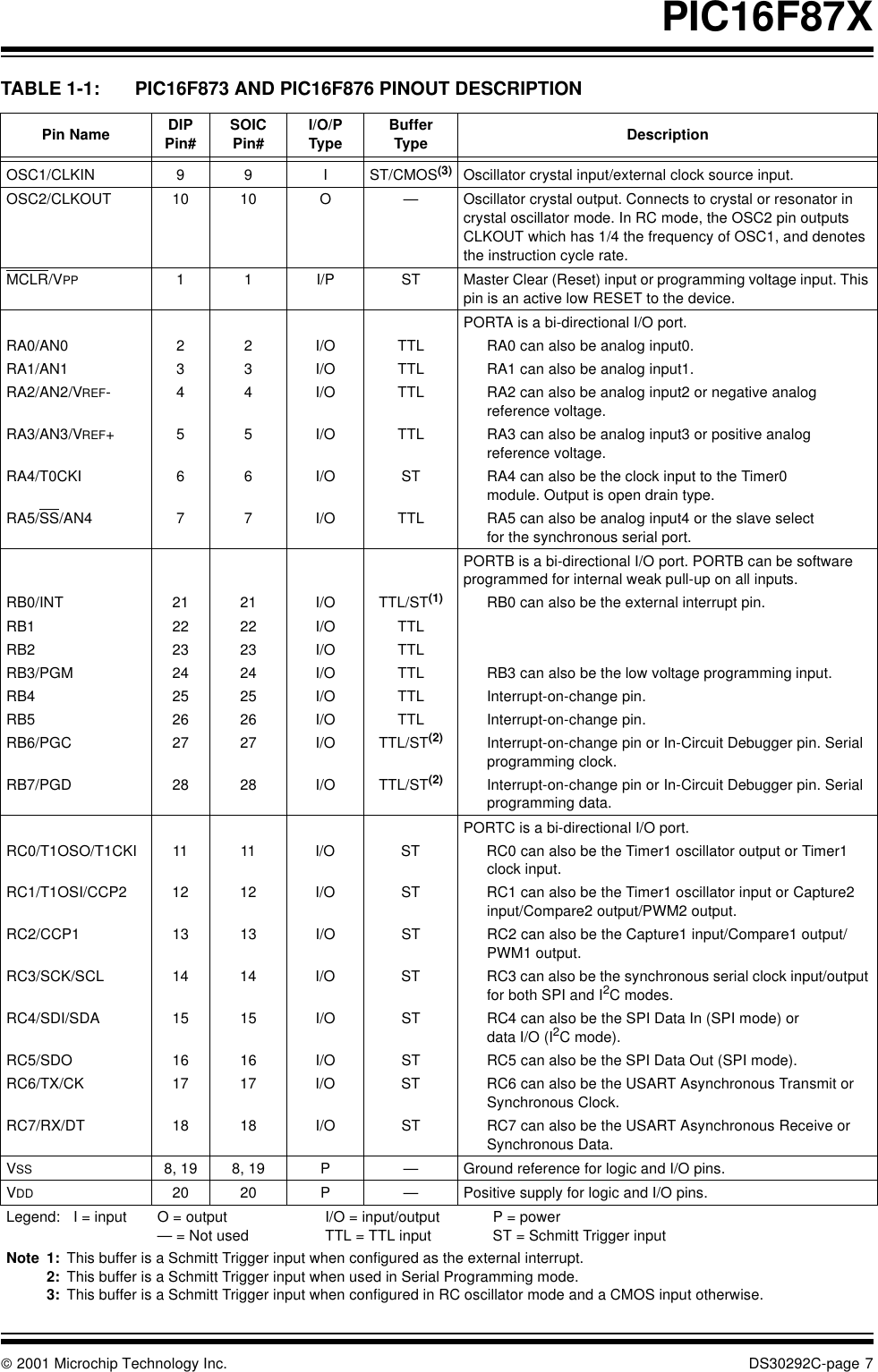
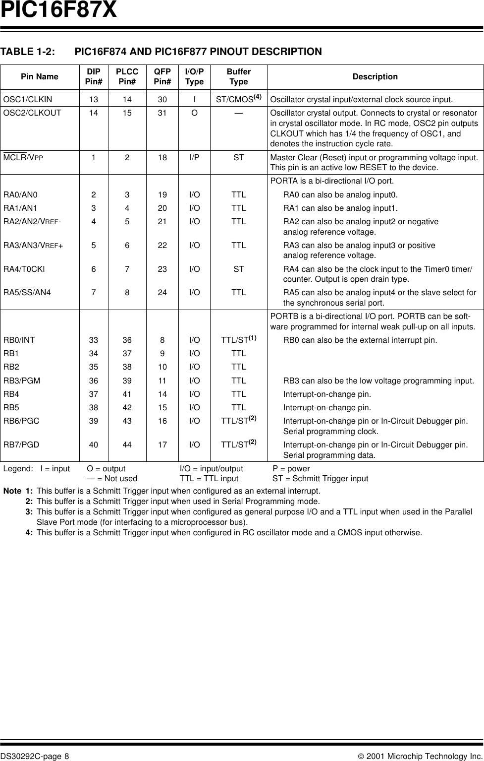
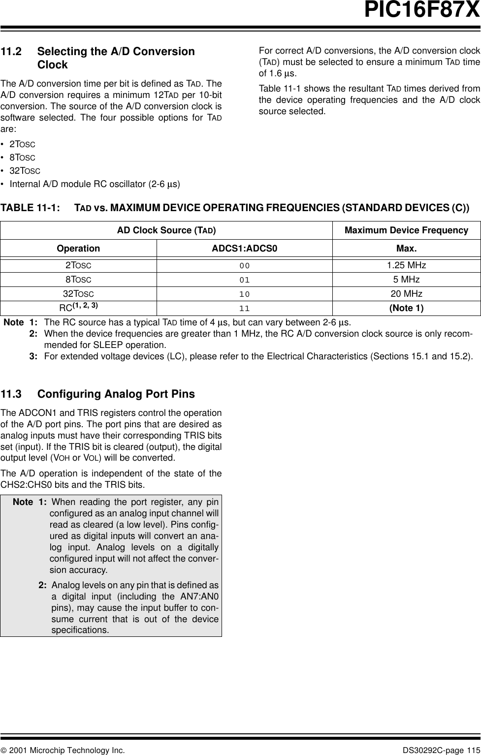
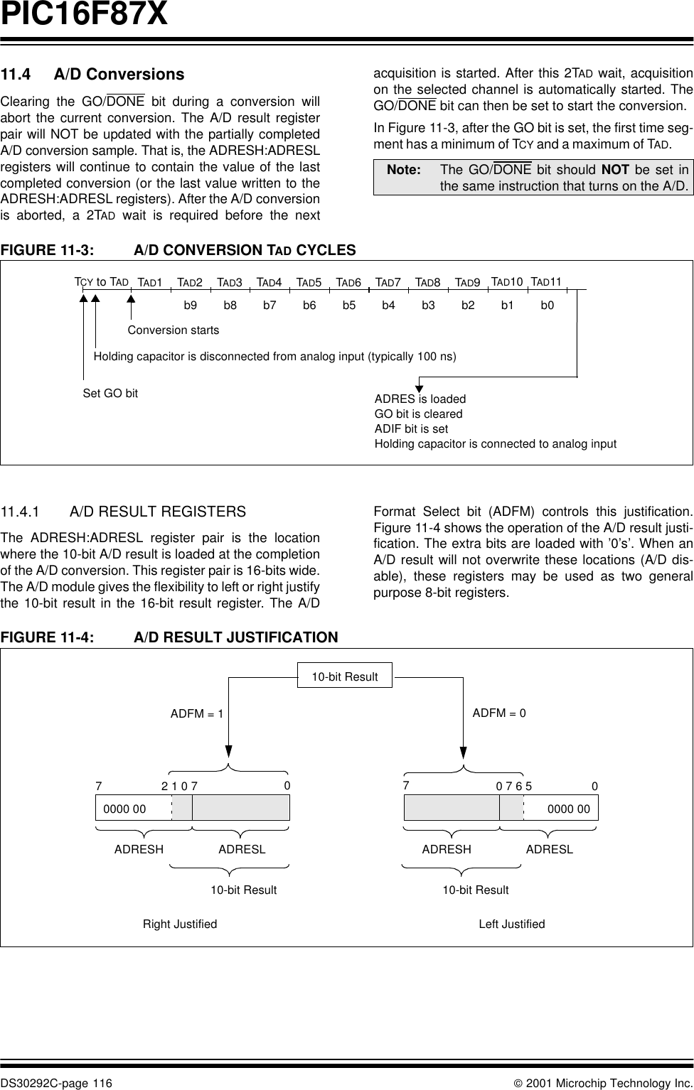
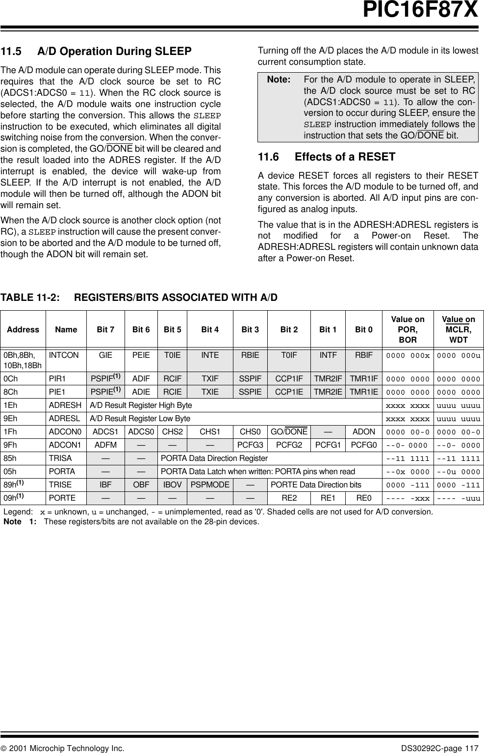
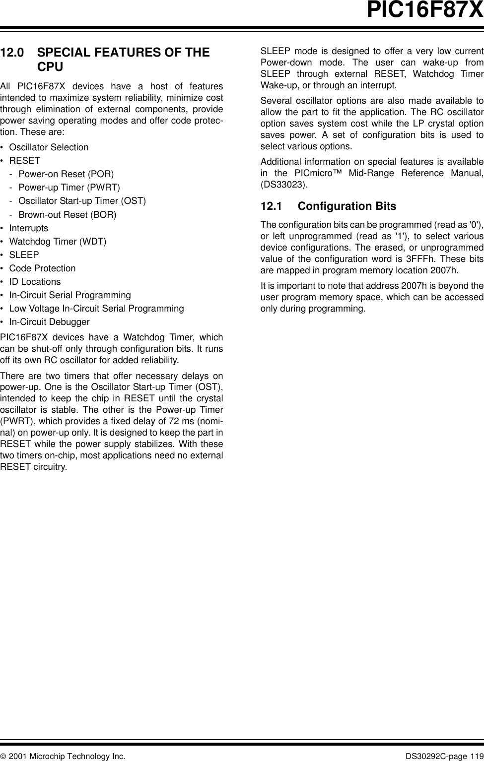
 2001 Microchip Technology Inc. DS30292C-page 7PIC16F87X TABLE 1-1: PIC16F873 AND PIC16F876 PINOUT DESCRIPTIONPin Name DIPPin# SOICPin# I/O/PType BufferType DescriptionOSC1/CLKIN 9 9 I ST/CMOS(3) Oscillator crystal input/external clock source input.OSC2/CLKOUT 10 10 O —Oscillator crystal output. Connects to crystal or resonator in crystal oscillator mode. In RC mode, the OSC2 pin outputs CLKOUT which has 1/4 the frequency of OSC1, and denotes the instruction cycle rate.MCLR/VPP 1 1 I/P ST Master Clear (Reset) input or programming voltage input. This pin is an active low RESET to the device. PORTA is a bi-directional I/O port.RA0/AN0 2 2 I/O TTL RA0 can also be analog input0.RA1/AN1 3 3 I/O TTL RA1 can also be analog input1.RA2/AN2/VREF- 4 4 I/O TTL RA2 can also be analog input2 or negative analog reference voltage.RA3/AN3/VREF+ 5 5 I/O TTL RA3 can also be analog input3 or positive analogreference voltage.RA4/T0CKI 6 6 I/O ST RA4 can also be the clock input to the Timer0 module. Output is open drain type.RA5/SS/AN4 7 7 I/O TTL RA5 can also be analog input4 or the slave selectfor the synchronous serial port.PORTB is a bi-directional I/O port. PORTB can be software programmed for internal weak pull-up on all inputs. RB0/INT 21 21 I/O TTL/ST(1) RB0 can also be the external interrupt pin.RB1 22 22 I/O TTLRB2 23 23 I/O TTLRB3/PGM 24 24 I/O TTL RB3 can also be the low voltage programming input.RB4 25 25 I/O TTL Interrupt-on-change pin.RB5 26 26 I/O TTL Interrupt-on-change pin.RB6/PGC 27 27 I/O TTL/ST(2) Interrupt-on-change pin or In-Circuit Debugger pin. Serial programming clock.RB7/PGD 28 28 I/O TTL/ST(2) Interrupt-on-change pin or In-Circuit Debugger pin. Serial programming data.PORTC is a bi-directional I/O port.RC0/T1OSO/T1CKI 11 11 I/O ST RC0 can also be the Timer1 oscillator output or Timer1 clock input.RC1/T1OSI/CCP2 12 12 I/O ST RC1 can also be the Timer1 oscillator input or Capture2 input/Compare2 output/PWM2 output.RC2/CCP1 13 13 I/O ST RC2 can also be the Capture1 input/Compare1 output/PWM1 output.RC3/SCK/SCL 14 14 I/O ST RC3 can also be the synchronous serial clock input/output for both SPI and I2C modes.RC4/SDI/SDA 15 15 I/O ST RC4 can also be the SPI Data In (SPI mode) or data I/O (I2C mode).RC5/SDO 16 16 I/O ST RC5 can also be the SPI Data Out (SPI mode).RC6/TX/CK 17 17 I/O ST RC6 can also be the USART Asynchronous Transmit or Synchronous Clock.RC7/RX/DT 18 18 I/O ST RC7 can also be the USART Asynchronous Receive or Synchronous Data.VSS 8, 19 8, 19 P —Ground reference for logic and I/O pins.VDD 20 20 P —Positive supply for logic and I/O pins.Legend: I = input O = output I/O = input/output P = power— = Not used TTL = TTL input ST = Schmitt Trigger inputNote 1: This buffer is a Schmitt Trigger input when configured as the external interrupt.2: This buffer is a Schmitt Trigger input when used in Serial Programming mode.3: This buffer is a Schmitt Trigger input when configured in RC oscillator mode and a CMOS input otherwise.
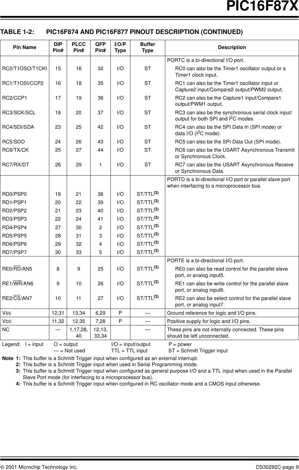
PIC16F87XDS30292C-page 8  2001 Microchip Technology Inc.TABLE 1-2: PIC16F874 AND PIC16F877 PINOUT DESCRIPTIONPin Name DIPPin# PLCCPin# QFPPin# I/O/PType BufferType DescriptionOSC1/CLKIN 13 14 30 I ST/CMOS(4) Oscillator crystal input/external clock source input.OSC2/CLKOUT 14 15 31 O —Oscillator crystal output. Connects to crystal or resonator in crystal oscillator mode. In RC mode, OSC2 pin outputs CLKOUT which has 1/4 the frequency of OSC1, and denotes the instruction cycle rate.MCLR/VPP 1 2 18 I/P ST Master Clear (Reset) input or programming voltage input. This pin is an active low RESET to the device. PORTA is a bi-directional I/O port.RA0/AN0 2 3 19 I/O TTL RA0 can also be analog input0.RA1/AN1 3 4 20 I/O TTL RA1 can also be analog input1.RA2/AN2/VREF- 4 5 21 I/O TTL RA2 can also be analog input2 or negative analog reference voltage.RA3/AN3/VREF+ 5 6 22 I/O TTL RA3 can also be analog input3 or positive analog reference voltage.RA4/T0CKI 6 7 23 I/O ST RA4 can also be the clock input to the Timer0 timer/counter. Output is open drain type.RA5/SS/AN4 7 8 24 I/O TTL RA5 can also be analog input4 or the slave select for the synchronous serial port.PORTB is a bi-directional I/O port. PORTB can be soft-ware programmed for internal weak pull-up on all inputs. RB0/INT 33 36 8 I/O TTL/ST(1) RB0 can also be the external interrupt pin.RB1 34 37 9 I/O TTLRB2 35 38 10 I/O TTLRB3/PGM 36 39 11 I/O TTL RB3 can also be the low voltage programming input.RB4 37 41 14 I/O TTL Interrupt-on-change pin.RB5 38 42 15 I/O TTL Interrupt-on-change pin.RB6/PGC 39 43 16 I/O TTL/ST(2) Interrupt-on-change pin or In-Circuit Debugger pin. Serial programming clock.RB7/PGD 40 44 17 I/O TTL/ST(2) Interrupt-on-change pin or In-Circuit Debugger pin. Serial programming data.Legend: I = input O = output I/O = input/output P = power— = Not used TTL = TTL input ST = Schmitt Trigger inputNote 1: This buffer is a Schmitt Trigger input when configured as an external interrupt.2: This buffer is a Schmitt Trigger input when used in Serial Programming mode.3: This buffer is a Schmitt Trigger input when configured as general purpose I/O and a TTL input when used in the Parallel Slave Port mode (for interfacing to a microprocessor bus).4: This buffer is a Schmitt Trigger input when configured in RC oscillator mode and a CMOS input otherwise.
 2001 Microchip Technology Inc. DS30292C-page 9PIC16F87XPORTC is a bi-directional I/O port.RC0/T1OSO/T1CKI 15 16 32 I/O ST RC0 can also be the Timer1 oscillator output or a Timer1 clock input.RC1/T1OSI/CCP2 16 18 35 I/O ST RC1 can also be the Timer1 oscillator input or Capture2 input/Compare2 output/PWM2 output.RC2/CCP1 17 19 36 I/O ST RC2 can also be the Capture1 input/Compare1 output/PWM1 output.RC3/SCK/SCL 18 20 37 I/O ST RC3 can also be the synchronous serial clock input/output for both SPI and I2C modes.RC4/SDI/SDA 23 25 42 I/O ST RC4 can also be the SPI Data In (SPI mode) or data I/O (I2C mode).RC5/SDO 24 26 43 I/O ST RC5 can also be the SPI Data Out (SPI mode).RC6/TX/CK 25 27 44 I/O ST RC6 can also be the USART Asynchronous Transmit or Synchronous Clock.RC7/RX/DT 26 29 1 I/O ST RC7 can also be the USART Asynchronous Receive or Synchronous Data.PORTD is a bi-directional I/O port or parallel slave port when interfacing to a microprocessor bus.RD0/PSP0 19 21 38 I/O ST/TTL(3)RD1/PSP1 20 22 39 I/O ST/TTL(3)RD2/PSP2 21 23 40 I/O ST/TTL(3)RD3/PSP3 22 24 41 I/O ST/TTL(3)RD4/PSP4 27 30 2 I/O ST/TTL(3)RD5/PSP5 28 31 3 I/O ST/TTL(3)RD6/PSP6 29 32 4 I/O ST/TTL(3)RD7/PSP7 30 33 5 I/O ST/TTL(3)PORTE is a bi-directional I/O port.RE0/RD/AN5 8 9 25 I/O ST/TTL(3) RE0 can also be read control for the parallel slave port, or analog input5.RE1/WR/AN6 9 10 26 I/O ST/TTL(3) RE1 can also be write control for the parallel slave port, or analog input6.RE2/CS/AN7 10 11 27 I/O ST/TTL(3) RE2 can also be select control for the parallel slave port, or analog input7.VSS 12,31 13,34 6,29 P —Ground reference for logic and I/O pins.VDD 11,32 12,35 7,28 P —Positive supply for logic and I/O pins.NC —1,17,28,4012,13,33,34—These pins are not internally connected. These pins should be left unconnected.TABLE 1-2: PIC16F874 AND PIC16F877 PINOUT DESCRIPTION (CONTINUED)Pin Name DIPPin# PLCCPin# QFPPin# I/O/PType BufferType DescriptionLegend: I = input O = output I/O = input/output P = power— = Not used TTL = TTL input ST = Schmitt Trigger inputNote 1: This buffer is a Schmitt Trigger input when configured as an external interrupt.2: This buffer is a Schmitt Trigger input when used in Serial Programming mode.3: This buffer is a Schmitt Trigger input when configured as general purpose I/O and a TTL input when used in the Parallel Slave Port mode (for interfacing to a microprocessor bus).4: This buffer is a Schmitt Trigger input when configured in RC oscillator mode and a CMOS input otherwise.
PIC16F87XDS30292C-page 10  2001 Microchip Technology Inc.NOTES:
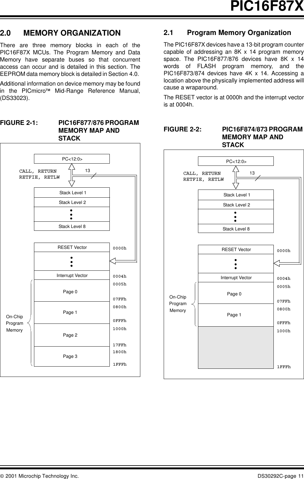
 2001 Microchip Technology Inc. DS30292C-page 11PIC16F87X2.0 MEMORY ORGANIZATIONThere are three memory blocks in each of thePIC16F87X MCUs. The Program Memory and DataMemory have separate buses so that concurrentaccess can occur and is detailed in this section. TheEEPROM data memory block is detailed in Section 4.0. Additional information on device memory may be foundin the PICmicro Mid-Range Reference Manual,(DS33023).FIGURE 2-1: PIC16F877/876 PROGRAM MEMORY MAP AND STACK 2.1 Program Memory OrganizationThe PIC16F87X devices have a 13-bit program countercapable of addressing an 8K x 14 program memoryspace. The PIC16F877/876 devices have 8K x 14words of FLASH program memory, and thePIC16F873/874 devices have 4K x 14. Accessing alocation above the physically implemented address willcause a wraparound. The RESET vector is at 0000h and the interrupt vectoris at 0004h.FIGURE 2-2: PIC16F874/873 PROGRAM MEMORY MAP AND STACK   PC<12:0>130000h0004h0005hStack Level 1Stack Level 8RESET VectorInterrupt VectorOn-ChipCALL, RETURNRETFIE, RETLW1FFFhStack Level 2ProgramMemoryPage 0Page 1Page 2Page 307FFh0800h0FFFh1000h17FFh1800hPC<12:0>130000h0004h0005hStack Level 1Stack Level 8RESET VectorInterrupt VectorOn-ChipCALL, RETURNRETFIE, RETLW1FFFhStack Level 2ProgramMemoryPage 0Page 107FFh0800h0FFFh1000h
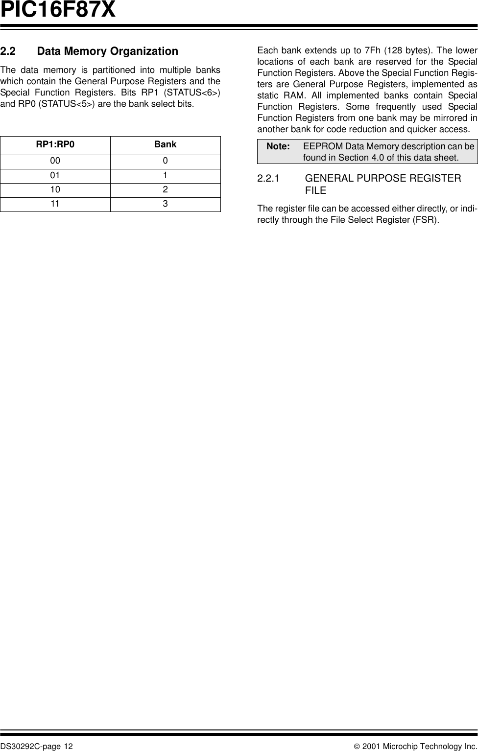
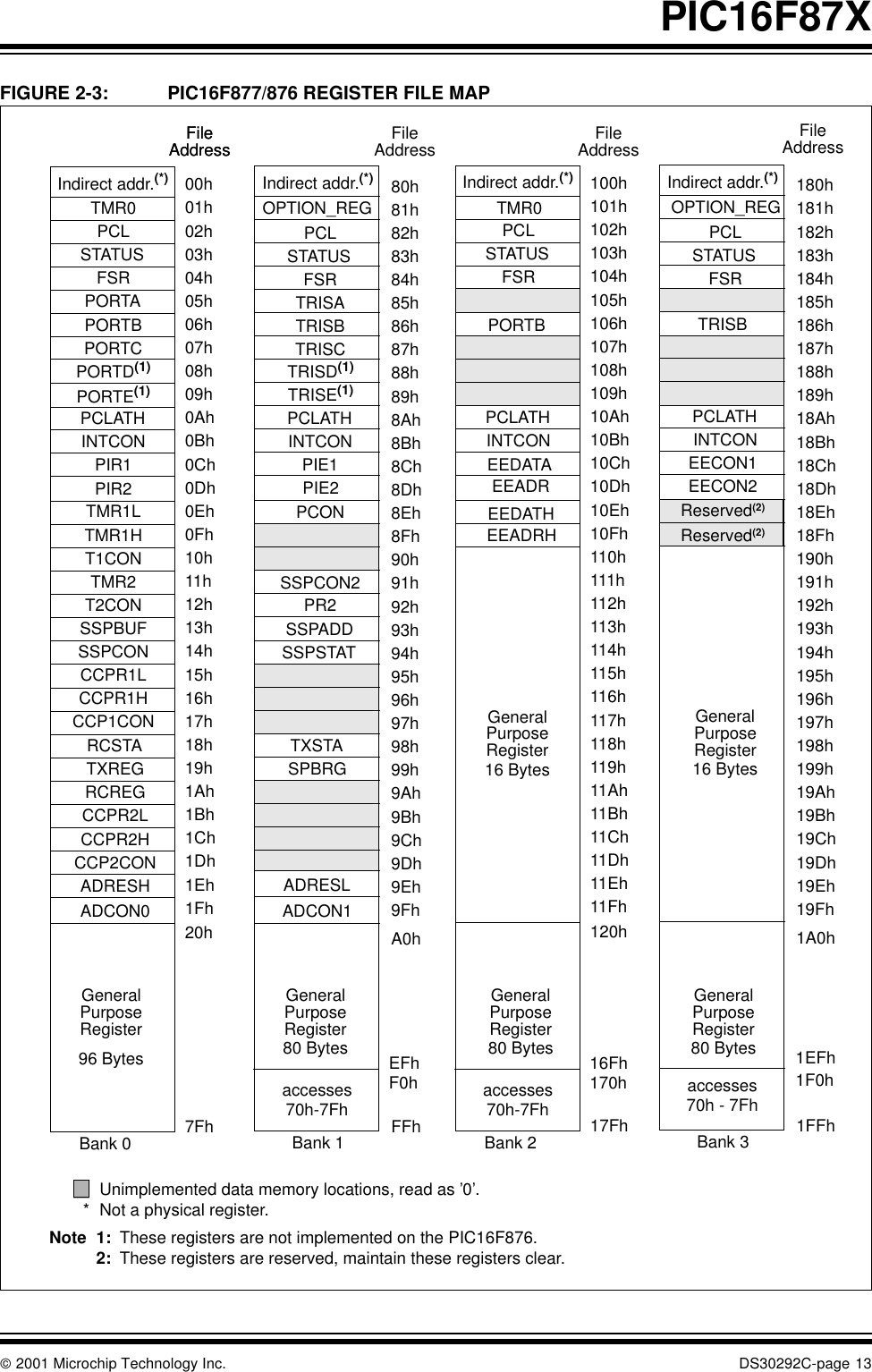
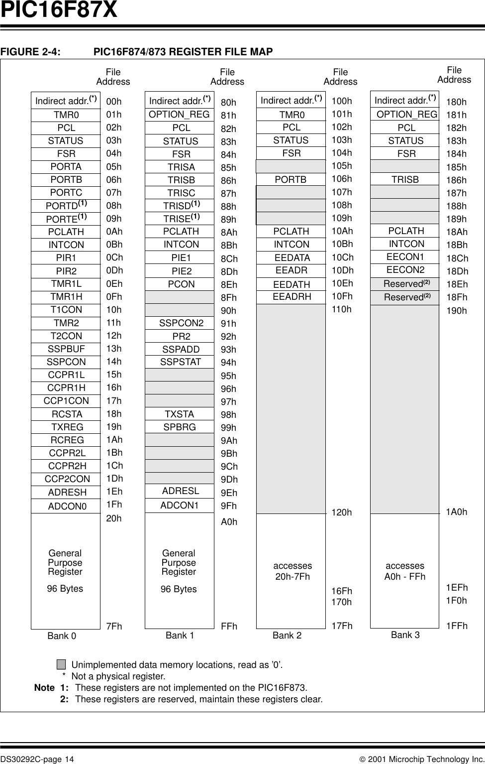
PIC16F87XDS30292C-page 12  2001 Microchip Technology Inc.2.2 Data Memory OrganizationThe data memory is partitioned into multiple bankswhich contain the General Purpose Registers and theSpecial Function Registers. Bits RP1 (STATUS<6>)and RP0 (STATUS<5>) are the bank select bits.Each bank extends up to 7Fh (128 bytes). The lowerlocations of each bank are reserved for the SpecialFunction Registers. Above the Special Function Regis-ters are General Purpose Registers, implemented asstatic RAM. All implemented banks contain SpecialFunction Registers. Some frequently used SpecialFunction Registers from one bank may be mirrored inanother bank for code reduction and quicker access. 2.2.1 GENERAL PURPOSE REGISTER FILEThe register file can be accessed either directly, or indi-rectly through the File Select Register (FSR). RP1:RP0 Bank00 001 110 211 3Note: EEPROM Data Memory description can befound in Section 4.0 of this data sheet.
 2001 Microchip Technology Inc. DS30292C-page 13PIC16F87XFIGURE 2-3: PIC16F877/876 REGISTER FILE MAP Indirect addr.(*)TMR0PCLSTATUSFSRPORTAPORTBPORTCPCLATHINTCONPIR1TMR1LTMR1HT1CONTMR2T2CONSSPBUFSSPCONCCPR1LCCPR1HCCP1CONOPTION_REGPCLSTATUSFSRTRISATRISBTRISCPCLATHINTCONPIE1PCONPR2SSPADDSSPSTAT00h01h02h03h04h05h06h07h08h09h0Ah0Bh0Ch0Dh0Eh0Fh10h11h12h13h14h15h16h17h18h19h1Ah1Bh1Ch1Dh1Eh1Fh80h81h82h83h84h85h86h87h88h89h8Ah8Bh8Ch8Dh8Eh8Fh90h91h92h93h94h95h96h97h98h99h9Ah9Bh9Ch9Dh9Eh9Fh20h A0h7Fh FFhBank 0 Bank 1  Unimplemented data memory locations, read as ’0’. * Not a physical register.Note 1: These registers are not implemented on the PIC16F876.2: These registers are reserved, maintain these registers clear.FileAddressIndirect addr.(*) Indirect addr.(*)PCLSTATUSFSRPCLATHINTCONPCLSTATUSFSRPCLATHINTCON100h101h102h103h104h105h106h107h108h109h10Ah10Bh10Ch10Dh10Eh10Fh110h111h112h113h114h115h116h117h118h119h11Ah11Bh11Ch11Dh11Eh11Fh180h181h182h183h184h185h186h187h188h189h18Ah18Bh18Ch18Dh18Eh18Fh190h191h192h193h194h195h196h197h198h199h19Ah19Bh19Ch19Dh19Eh19Fh120h 1A0h17Fh 1FFhBank 2 Bank 3Indirect addr.(*)PORTD(1)PORTE(1) TRISD(1)ADRESL TRISE(1)TMR0 OPTION_REGPIR2 PIE2RCSTATXREGRCREGCCPR2LCCPR2HCCP2CONADRESHADCON0TXSTASPBRGADCON1GeneralPurposeRegisterGeneralPurposeRegisterGeneralPurposeRegisterGeneralPurposeRegister1EFh1F0haccesses70h - 7FhEFhF0haccesses70h-7Fh16Fh170haccesses70h-7FhGeneralPurposeRegisterGeneralPurposeRegisterTRISBPORTB96 Bytes 80 Bytes 80 Bytes 80 Bytes16 Bytes 16 BytesSSPCON2EEDATAEEADREECON1EECON2EEDATHEEADRHReserved(2)Reserved(2)FileAddress FileAddress FileAddressFileAddress
PIC16F87XDS30292C-page 14  2001 Microchip Technology Inc.FIGURE 2-4: PIC16F874/873 REGISTER FILE MAP  Indirect addr.(*)TMR0PCLSTATUSFSRPORTAPORTBPORTCPCLATHINTCONPIR1TMR1LTMR1HT1CONTMR2T2CONSSPBUFSSPCONCCPR1LCCPR1HCCP1CONOPTION_REGPCLSTATUSFSRTRISATRISBTRISCPCLATHINTCONPIE1PCONPR2SSPADDSSPSTAT00h01h02h03h04h05h06h07h08h09h0Ah0Bh0Ch0Dh0Eh0Fh10h11h12h13h14h15h16h17h18h19h1Ah1Bh1Ch1Dh1Eh1Fh80h81h82h83h84h85h86h87h88h89h8Ah8Bh8Ch8Dh8Eh8Fh90h91h92h93h94h95h96h97h98h99h9Ah9Bh9Ch9Dh9Eh9Fh20h A0h7Fh FFhBank 0 Bank 1Indirect addr.(*) Indirect addr.(*)PCLSTATUSFSRPCLATHINTCONPCLSTATUSFSRPCLATHINTCON100h101h102h103h104h105h106h107h108h109h10Ah10Bh180h181h182h183h184h185h186h187h188h189h18Ah18Bh17Fh 1FFhBank 2 Bank 3Indirect addr.(*)PORTD(1)PORTE(1) TRISD(1)ADRESLTRISE(1)TMR0 OPTION_REGPIR2 PIE2RCSTATXREGRCREGCCPR2LCCPR2HCCP2CONADRESHADCON0TXSTASPBRGADCON1GeneralPurposeRegisterGeneralPurposeRegister1EFh1F0haccessesA0h - FFh16Fh170haccesses20h-7FhTRISBPORTB96 Bytes 96 BytesSSPCON210Ch10Dh10Eh10Fh110h18Ch18Dh18Eh18Fh190hEEDATAEEADREECON1EECON2EEDATHEEADRHReserved(2)Reserved(2)  Unimplemented data memory locations, read as ’0’. * Not a physical register.Note 1: These registers are not implemented on the PIC16F873.2: These registers are reserved, maintain these registers clear.120h 1A0hFileAddressFileAddress FileAddressFileAddress
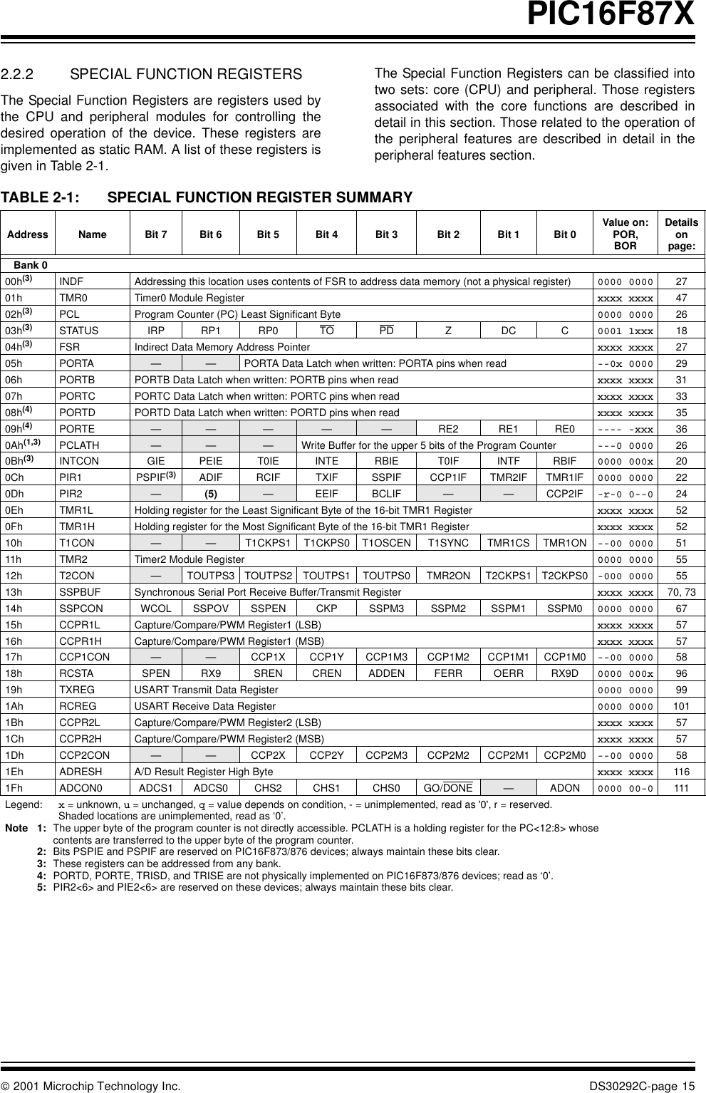
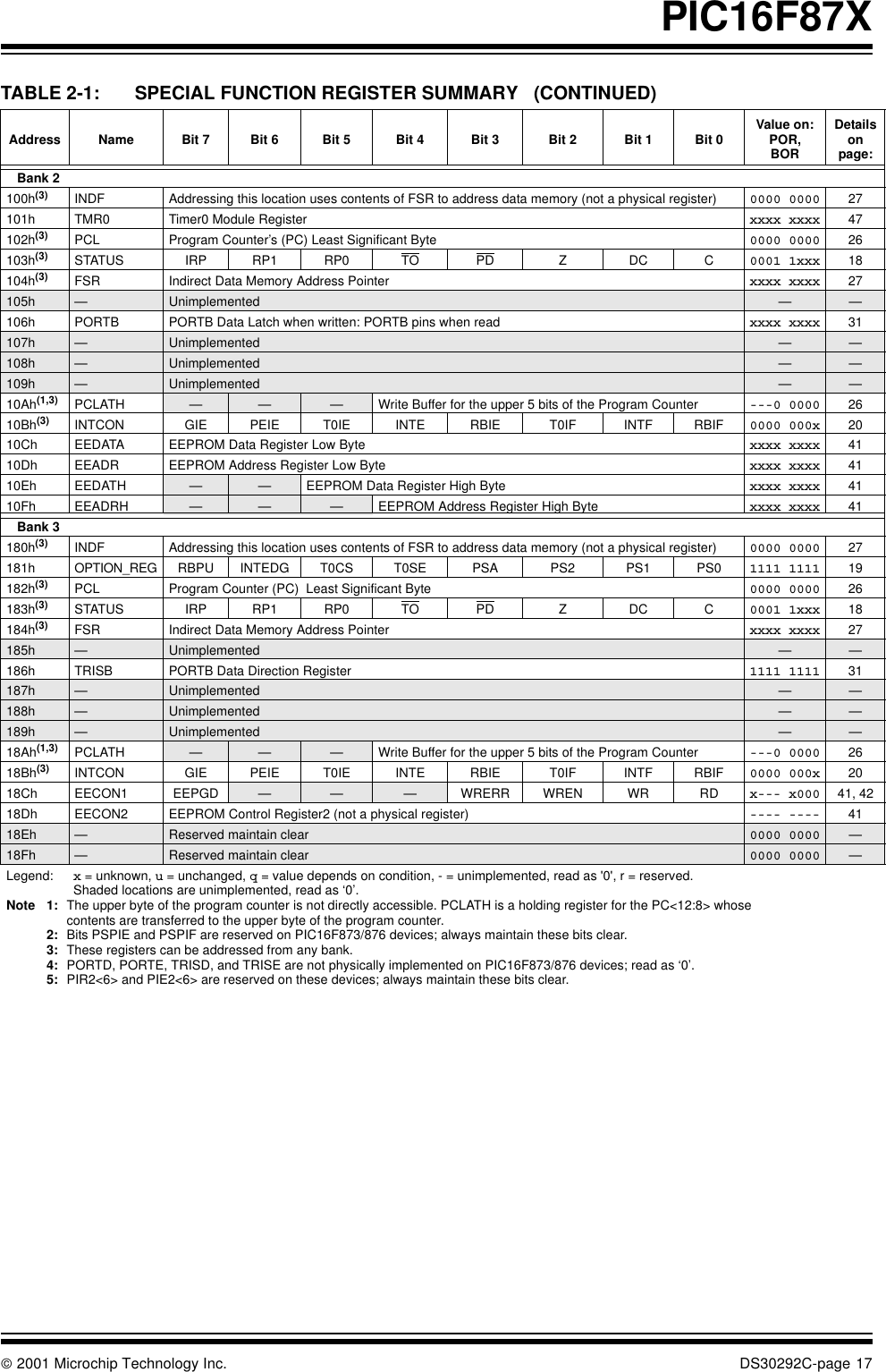
 2001 Microchip Technology Inc. DS30292C-page 15PIC16F87X2.2.2 SPECIAL FUNCTION REGISTERSThe Special Function Registers are registers used bythe CPU and peripheral modules for controlling thedesired operation of the device. These registers areimplemented as static RAM. A list of these registers isgiven in Table 2-1.The Special Function Registers can be classified intotwo sets: core (CPU) and peripheral. Those registersassociated with the core functions are described indetail in this section. Those related to the operation ofthe peripheral features are described in detail in theperipheral features section.TABLE 2-1: SPECIAL FUNCTION REGISTER SUMMARY  Address  Name Bit 7 Bit 6 Bit 5 Bit 4 Bit 3 Bit 2  Bit 1 Bit 0 Value on:POR,BORDetails on page:   Bank 000h(3) INDF Addressing this location uses contents of FSR to address data memory (not a physical register) 0000 0000 2701h TMR0 Timer0 Module Register xxxx xxxx 4702h(3) PCL Program Counter (PC) Least Significant Byte 0000 0000 2603h(3) STATUS IRP RP1 RP0 TO PD ZDCC0001 1xxx 1804h(3) FSR Indirect Data Memory Address Pointer xxxx xxxx 2705h PORTA — — PORTA Data Latch when written: PORTA pins when read --0x 0000 2906h PORTB PORTB Data Latch when written: PORTB pins when read xxxx xxxx 3107h PORTC PORTC Data Latch when written: PORTC pins when read xxxx xxxx 3308h(4) PORTD PORTD Data Latch when written: PORTD pins when read xxxx xxxx 3509h(4) PORTE — — — — — RE2 RE1 RE0 ---- -xxx 360Ah(1,3) PCLATH — — — Write Buffer for the upper 5 bits of the Program Counter ---0 0000 260Bh(3) INTCON GIE PEIE T0IE INTE RBIE T0IF INTF RBIF 0000 000x 200Ch PIR1 PSPIF(3) ADIF RCIF TXIF SSPIF CCP1IF TMR2IF TMR1IF 0000 0000 220Dh PIR2 —(5) —EEIF BCLIF — — CCP2IF -r-0 0--0 240Eh TMR1L Holding register for the Least Significant Byte of the 16-bit TMR1 Register xxxx xxxx 520Fh TMR1H Holding register for the Most Significant Byte of the 16-bit TMR1 Register xxxx xxxx 5210h T1CON — — T1CKPS1 T1CKPS0 T1OSCEN T1SYNC TMR1CS TMR1ON --00 0000 5111h TMR2 Timer2 Module Register 0000 0000 5512h T2CON —TOUTPS3 TOUTPS2 TOUTPS1 TOUTPS0 TMR2ON T2CKPS1 T2CKPS0 -000 0000 5513h SSPBUF Synchronous Serial Port Receive Buffer/Transmit Register xxxx xxxx 70, 7314h SSPCON WCOL SSPOV SSPEN CKP SSPM3 SSPM2 SSPM1 SSPM0 0000 0000 6715h CCPR1L Capture/Compare/PWM Register1 (LSB) xxxx xxxx 5716h CCPR1H Capture/Compare/PWM Register1 (MSB) xxxx xxxx 5717h CCP1CON — — CCP1X CCP1Y CCP1M3 CCP1M2 CCP1M1 CCP1M0 --00 0000 5818h RCSTA SPEN RX9 SREN CREN ADDEN FERR OERR RX9D 0000 000x 9619h TXREG USART Transmit Data Register 0000 0000 991Ah RCREG USART Receive Data Register 0000 0000 1011Bh CCPR2L Capture/Compare/PWM Register2 (LSB) xxxx xxxx 571Ch CCPR2H Capture/Compare/PWM Register2 (MSB) xxxx xxxx 571Dh CCP2CON — — CCP2X CCP2Y CCP2M3 CCP2M2 CCP2M1 CCP2M0 --00 0000 581Eh ADRESH A/D Result Register High Byte xxxx xxxx 1161Fh ADCON0 ADCS1 ADCS0 CHS2 CHS1 CHS0 GO/DONE —ADON 0000 00-0 111Legend: x = unknown, u = unchanged, q = value depends on condition, - = unimplemented, read as '0', r = reserved. Shaded locations are unimplemented, read as ‘0’.Note 1: The upper byte of the program counter is not directly accessible. PCLATH is a holding register for the PC<12:8> whose contents are transferred to the upper byte of the program counter.2: Bits PSPIE and PSPIF are reserved on PIC16F873/876 devices; always maintain these bits clear.3: These registers can be addressed from any bank.4: PORTD, PORTE, TRISD, and TRISE are not physically implemented on PIC16F873/876 devices; read as ‘0’.5: PIR2<6> and PIE2<6> are reserved on these devices; always maintain these bits clear.
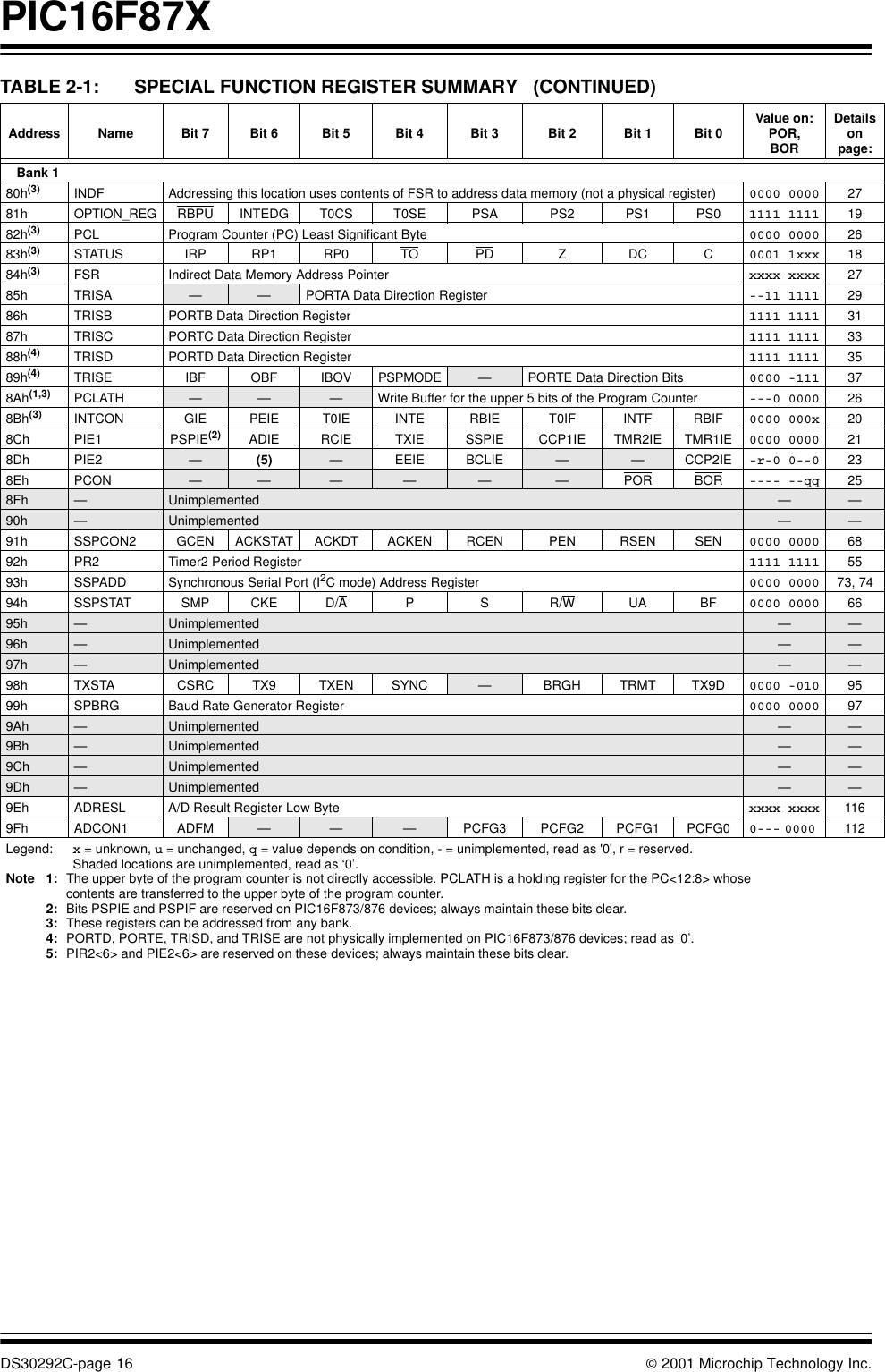
PIC16F87XDS30292C-page 16  2001 Microchip Technology Inc.   Bank 180h(3) INDF Addressing this location uses contents of FSR to address data memory (not a physical register) 0000 0000 2781h OPTION_REG RBPU INTEDG T0CS T0SE PSA PS2 PS1 PS0 1111 1111 1982h(3) PCL Program Counter (PC) Least Significant Byte 0000 0000 2683h(3) STATUS IRP RP1 RP0 TO PD ZDCC0001 1xxx 1884h(3) FSR Indirect Data Memory Address Pointer xxxx xxxx 2785h TRISA — — PORTA Data Direction Register --11 1111 2986h TRISB PORTB Data Direction Register 1111 1111 3187h TRISC PORTC Data Direction Register 1111 1111 3388h(4) TRISD PORTD Data Direction Register 1111 1111 3589h(4) TRISE IBF OBF IBOV PSPMODE —PORTE Data Direction Bits 0000 -111 378Ah(1,3) PCLATH — — — Write Buffer for the upper 5 bits of the Program Counter ---0 0000 268Bh(3) INTCON GIE PEIE T0IE INTE RBIE T0IF INTF RBIF 0000 000x 208Ch PIE1 PSPIE(2) ADIE RCIE TXIE SSPIE CCP1IE TMR2IE TMR1IE 0000 0000 218Dh PIE2 —(5) —EEIE BCLIE — — CCP2IE -r-0 0--0 238Eh PCON — — — — — — POR BOR ---- --qq 258Fh —Unimplemented — —90h —Unimplemented — —91h SSPCON2 GCEN ACKSTAT ACKDT ACKEN RCEN PEN RSEN SEN 0000 0000 6892h PR2 Timer2 Period Register 1111 1111 5593h SSPADD Synchronous Serial Port (I2C mode) Address Register 0000 0000 73, 7494h SSPSTAT SMP CKE D/A PSR/WUA BF 0000 0000 6695h —Unimplemented — —96h —Unimplemented — —97h —Unimplemented — —98h TXSTA CSRC TX9 TXEN SYNC —BRGH TRMT TX9D 0000 -010 9599h SPBRG Baud Rate Generator Register 0000 0000 979Ah —Unimplemented — —9Bh —Unimplemented — —9Ch —Unimplemented — —9Dh —Unimplemented — —9Eh ADRESL A/D Result Register Low Byte xxxx xxxx 1169Fh ADCON1 ADFM — — — PCFG3 PCFG2 PCFG1 PCFG0 0--- 0000  112TABLE 2-1: SPECIAL FUNCTION REGISTER SUMMARY   (CONTINUED)Address  Name Bit 7 Bit 6 Bit 5 Bit 4 Bit 3 Bit 2  Bit 1 Bit 0 Value on:POR,BORDetails on page:Legend: x = unknown, u = unchanged, q = value depends on condition, - = unimplemented, read as '0', r = reserved. Shaded locations are unimplemented, read as ‘0’.Note 1: The upper byte of the program counter is not directly accessible. PCLATH is a holding register for the PC<12:8> whose contents are transferred to the upper byte of the program counter.2: Bits PSPIE and PSPIF are reserved on PIC16F873/876 devices; always maintain these bits clear.3: These registers can be addressed from any bank.4: PORTD, PORTE, TRISD, and TRISE are not physically implemented on PIC16F873/876 devices; read as ‘0’.5: PIR2<6> and PIE2<6> are reserved on these devices; always maintain these bits clear.
 2001 Microchip Technology Inc. DS30292C-page 17PIC16F87X   Bank 2100h(3) INDF Addressing this location uses contents of FSR to address data memory (not a physical register) 0000 0000 27101h TMR0 Timer0 Module Register xxxx xxxx 47102h(3) PCL Program Counter’s (PC) Least Significant Byte 0000 0000 26103h(3) STATUS IRP RP1 RP0 TO PD ZDCC0001 1xxx 18104h(3) FSR Indirect Data Memory Address Pointer xxxx xxxx 27105h —Unimplemented — —106h PORTB PORTB Data Latch when written: PORTB pins when read xxxx xxxx 31107h —Unimplemented — —108h —Unimplemented — —109h —Unimplemented — —10Ah(1,3) PCLATH — — — Write Buffer for the upper 5 bits of the Program Counter ---0 0000 2610Bh(3) INTCON GIE PEIE T0IE INTE RBIE T0IF INTF RBIF 0000 000x 2010Ch EEDATA EEPROM Data Register Low Byte xxxx xxxx 4110Dh EEADR EEPROM Address Register Low Byte xxxx xxxx 4110Eh EEDATH — — EEPROM Data Register High Byte xxxx xxxx 4110Fh EEADRH — — — EEPROM Address Register High Byte xxxx xxxx 41   Bank 3180h(3) INDF Addressing this location uses contents of FSR to address data memory (not a physical register) 0000 0000 27181h OPTION_REG RBPU INTEDG T0CS T0SE PSA PS2 PS1 PS0 1111 1111 19182h(3) PCL Program Counter (PC)  Least Significant Byte 0000 0000 26183h(3) STATUS IRP RP1 RP0 TO PD ZDCC0001 1xxx 18184h(3) FSR Indirect Data Memory Address Pointer xxxx xxxx 27185h —Unimplemented — —186h TRISB PORTB Data Direction Register 1111 1111 31187h —Unimplemented — —188h —Unimplemented — —189h —Unimplemented — —18Ah(1,3) PCLATH — — — Write Buffer for the upper 5 bits of the Program Counter ---0 0000 2618Bh(3) INTCON GIE PEIE T0IE INTE RBIE T0IF INTF RBIF 0000 000x 2018Ch EECON1 EEPGD — — — WRERR WREN WR RD x--- x000 41, 4218Dh EECON2 EEPROM Control Register2 (not a physical register) ---- ---- 4118Eh —Reserved maintain clear 0000 0000 —18Fh —Reserved maintain clear 0000 0000 —TABLE 2-1: SPECIAL FUNCTION REGISTER SUMMARY   (CONTINUED)Address  Name Bit 7 Bit 6 Bit 5 Bit 4 Bit 3 Bit 2  Bit 1 Bit 0 Value on:POR,BORDetails on page:Legend: x = unknown, u = unchanged, q = value depends on condition, - = unimplemented, read as '0', r = reserved. Shaded locations are unimplemented, read as ‘0’.Note 1: The upper byte of the program counter is not directly accessible. PCLATH is a holding register for the PC<12:8> whose contents are transferred to the upper byte of the program counter.2: Bits PSPIE and PSPIF are reserved on PIC16F873/876 devices; always maintain these bits clear.3: These registers can be addressed from any bank.4: PORTD, PORTE, TRISD, and TRISE are not physically implemented on PIC16F873/876 devices; read as ‘0’.5: PIR2<6> and PIE2<6> are reserved on these devices; always maintain these bits clear.
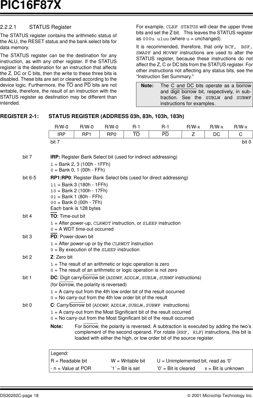
PIC16F87XDS30292C-page 18  2001 Microchip Technology Inc.2.2.2.1 STATUS RegisterThe STATUS register contains the arithmetic status ofthe ALU, the RESET status and the bank select bits fordata memory.The STATUS register can be the destination for anyinstruction, as with any other register. If the STATUSregister is the destination for an instruction that affectsthe Z, DC or C bits, then the write to these three bits isdisabled. These bits are set or cleared according to thedevice logic. Furthermore, the TO and PD bits are notwritable, therefore, the result of an instruction with theSTATUS register as destination may be different thanintended. For example, CLRF STATUS will clear the upper threebits and set the Z bit.   This leaves the STATUS registeras 000u u1uu (where u = unchanged).It is recommended, therefore, that only BCF, BSF,SWAPF and MOVWF instructions are used to alter theSTATUS register, because these instructions do notaffect the Z, C or DC bits from the STATUS register. Forother instructions not affecting any status bits, see the“Instruction Set Summary." REGISTER 2-1: STATUS REGISTER (ADDRESS 03h, 83h, 103h, 183h)                      Note: The C and DC bits operate as a borrowand digit borrow bit, respectively, in sub-traction. See the SUBLW and SUBWFinstructions for examples.R/W-0 R/W-0 R/W-0 R-1 R-1 R/W-x R/W-x R/W-xIRP RP1 RP0 TO PD ZDCCbit 7 bit 0bit 7 IRP: Register Bank Select bit (used for indirect addressing)1 = Bank 2, 3 (100h - 1FFh) 0 = Bank 0, 1 (00h - FFh) bit 6-5 RP1:RP0: Register Bank Select bits (used for direct addressing)11 = Bank 3 (180h - 1FFh) 10 = Bank 2 (100h - 17Fh) 01 = Bank 1 (80h - FFh)00 = Bank 0 (00h - 7Fh)Each bank is 128 bytesbit 4 TO: Time-out bit1 = After power-up, CLRWDT instruction, or SLEEP instruction0 = A WDT time-out occurredbit 3 PD: Power-down bit1 = After power-up or by the CLRWDT instruction0 = By execution of the SLEEP instructionbit 2 Z: Zero bit1 = The result of an arithmetic or logic operation is zero0 = The result of an arithmetic or logic operation is not zerobit 1 DC: Digit carry/borrow bit (ADDWF, ADDLW,SUBLW,SUBWF instructions) (for borrow, the polarity is reversed)1 = A carry-out from the 4th low order bit of the result occurred0 = No carry-out from the 4th low order bit of the resultbit 0 C: Carry/borrow bit (ADDWF, ADDLW,SUBLW,SUBWF instructions)1 = A carry-out from the Most Significant bit of the result occurred0 = No carry-out from the Most Significant bit of the result occurredNote: For borrow, the polarity is reversed. A subtraction is executed by adding the two’scomplement of the second operand. For rotate (RRF, RLF) instructions, this bit isloaded with either the high, or low order bit of the source register.Legend:R = Readable bit W = Writable bit U = Unimplemented bit, read as ‘0’- n = Value at POR ’1’ = Bit is set ’0’ = Bit is cleared x = Bit is unknown
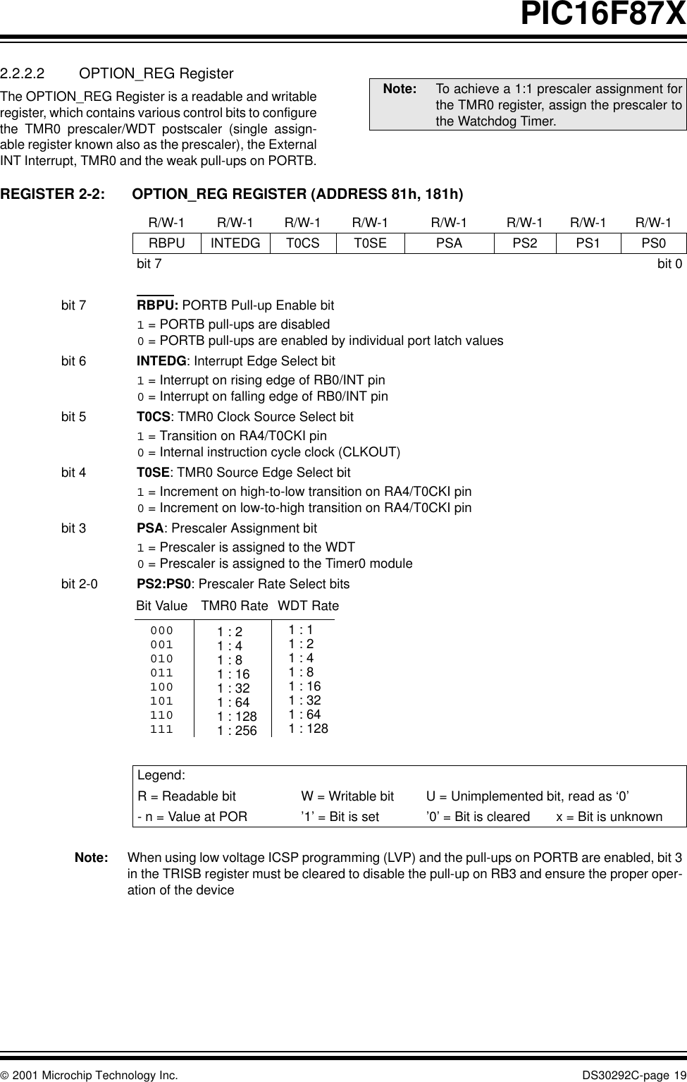
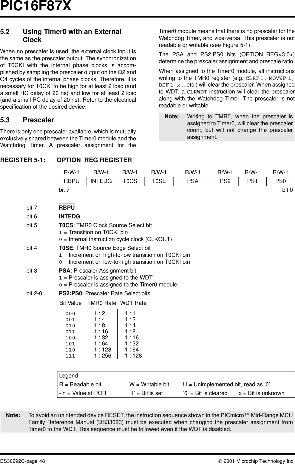
 2001 Microchip Technology Inc. DS30292C-page 19PIC16F87X2.2.2.2 OPTION_REG RegisterThe OPTION_REG Register is a readable and writableregister, which contains various control bits to configurethe TMR0 prescaler/WDT postscaler (single assign-able register known also as the prescaler), the ExternalINT Interrupt, TMR0 and the weak pull-ups on PORTB.REGISTER 2-2: OPTION_REG REGISTER (ADDRESS 81h, 181h)                     Note: To achieve a 1:1 prescaler assignment forthe TMR0 register, assign the prescaler tothe Watchdog Timer.R/W-1 R/W-1 R/W-1 R/W-1 R/W-1 R/W-1 R/W-1 R/W-1RBPU INTEDG T0CS T0SE PSA PS2 PS1 PS0bit 7 bit 0bit 7 RBPU: PORTB Pull-up Enable bit1 = PORTB pull-ups are disabled0 = PORTB pull-ups are enabled by individual port latch valuesbit 6 INTEDG: Interrupt Edge Select bit1 = Interrupt on rising edge of RB0/INT pin0 = Interrupt on falling edge of RB0/INT pinbit 5 T0CS: TMR0 Clock Source Select bit1 = Transition on RA4/T0CKI pin0 = Internal instruction cycle clock (CLKOUT)bit 4 T0SE: TMR0 Source Edge Select bit1 = Increment on high-to-low transition on RA4/T0CKI pin0 = Increment on low-to-high transition on RA4/T0CKI pinbit 3 PSA: Prescaler Assignment bit1 = Prescaler is assigned to the WDT0 = Prescaler is assigned to the Timer0 modulebit 2-0 PS2:PS0: Prescaler Rate Select bitsLegend:R = Readable bit W = Writable bit U = Unimplemented bit, read as ‘0’- n = Value at POR ’1’ = Bit is set ’0’ = Bit is cleared x = Bit is unknownNote: When using low voltage ICSP programming (LVP) and the pull-ups on PORTB are enabled, bit 3in the TRISB register must be cleared to disable the pull-up on RB3 and ensure the proper oper-ation of the device0000010100111001011101111 : 21 : 41 : 81 : 161 : 321 : 641 : 1281 : 2561 : 11 : 21 : 41 : 81 : 161 : 321 : 641 : 128Bit Value TMR0 Rate WDT Rate
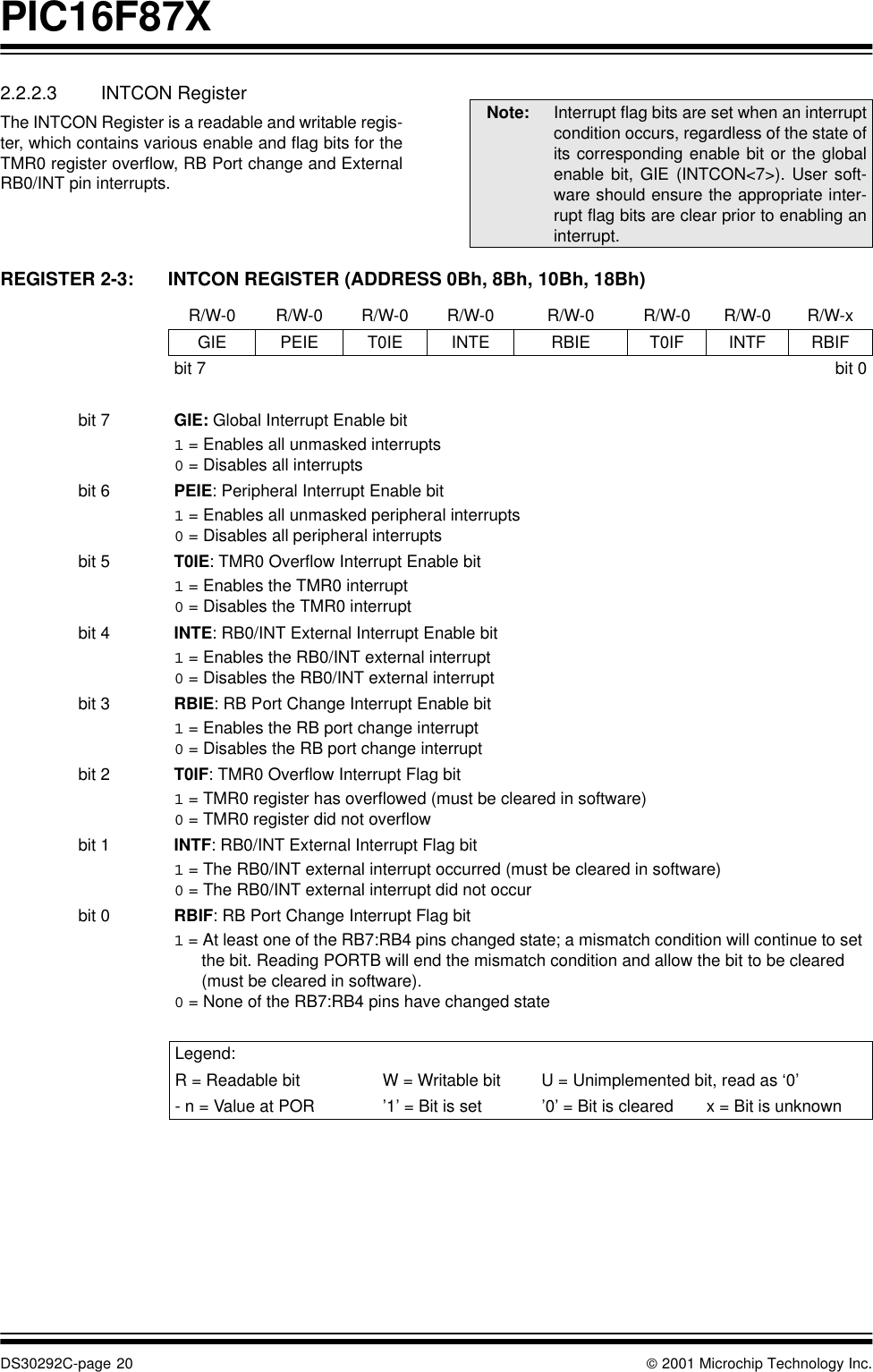
PIC16F87XDS30292C-page 20  2001 Microchip Technology Inc.2.2.2.3 INTCON RegisterThe INTCON Register is a readable and writable regis-ter, which contains various enable and flag bits for theTMR0 register overflow, RB Port change and ExternalRB0/INT pin interrupts. REGISTER 2-3: INTCON REGISTER (ADDRESS 0Bh, 8Bh, 10Bh, 18Bh)                     Note: Interrupt flag bits are set when an interruptcondition occurs, regardless of the state ofits corresponding enable bit or the globalenable bit, GIE (INTCON<7>). User soft-ware should ensure the appropriate inter-rupt flag bits are clear prior to enabling aninterrupt.R/W-0 R/W-0 R/W-0 R/W-0 R/W-0 R/W-0 R/W-0 R/W-xGIE PEIE T0IE INTE RBIE T0IF INTF RBIFbit 7 bit 0bit 7 GIE: Global Interrupt Enable bit1 = Enables all unmasked interrupts0 = Disables all interruptsbit 6 PEIE: Peripheral Interrupt Enable bit1 = Enables all unmasked peripheral interrupts0 = Disables all peripheral interruptsbit 5 T0IE: TMR0 Overflow Interrupt Enable bit1 = Enables the TMR0 interrupt0 = Disables the TMR0 interruptbit 4 INTE: RB0/INT External Interrupt Enable bit1 = Enables the RB0/INT external interrupt0 = Disables the RB0/INT external interruptbit 3 RBIE: RB Port Change Interrupt Enable bit1 = Enables the RB port change interrupt0 = Disables the RB port change interruptbit 2 T0IF: TMR0 Overflow Interrupt Flag bit1 = TMR0 register has overflowed (must be cleared in software)0 = TMR0 register did not overflowbit 1 INTF: RB0/INT External Interrupt Flag bit1 = The RB0/INT external interrupt occurred (must be cleared in software)0 = The RB0/INT external interrupt did not occurbit 0 RBIF: RB Port Change Interrupt Flag bit1 = At least one of the RB7:RB4 pins changed state; a mismatch condition will continue to set the bit. Reading PORTB will end the mismatch condition and allow the bit to be cleared (must be cleared in software).0 = None of the RB7:RB4 pins have changed stateLegend:R = Readable bit W = Writable bit U = Unimplemented bit, read as ‘0’- n = Value at POR ’1’ = Bit is set ’0’ = Bit is cleared x = Bit is unknown
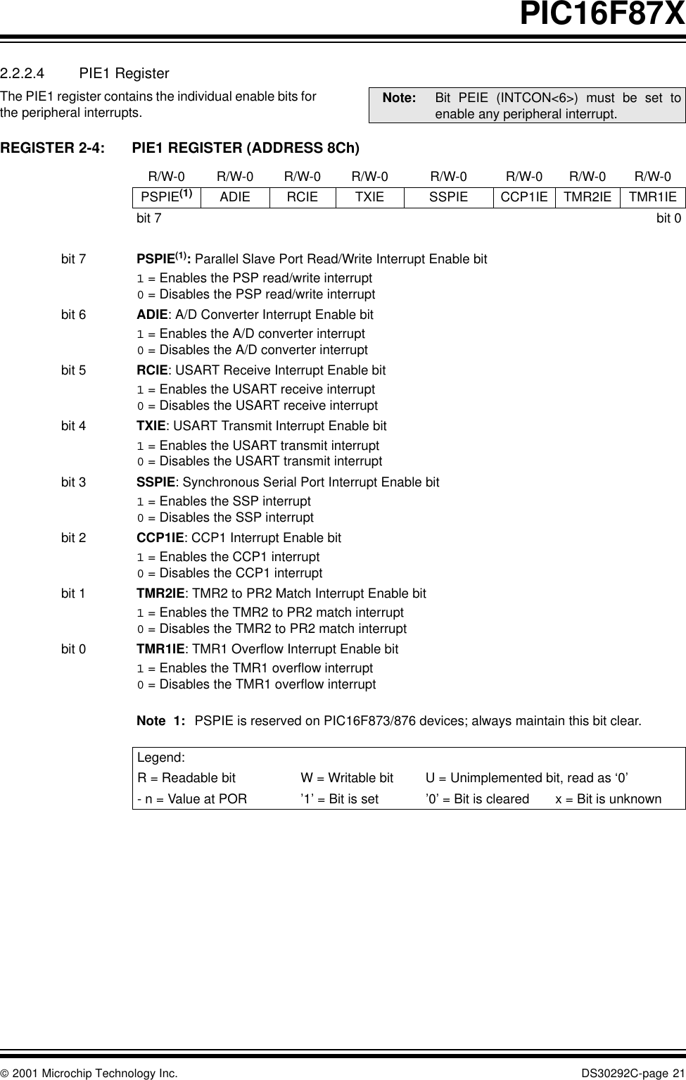
 2001 Microchip Technology Inc. DS30292C-page 21PIC16F87X2.2.2.4 PIE1 RegisterThe PIE1 register contains the individual enable bits forthe peripheral interrupts.REGISTER 2-4: PIE1 REGISTER (ADDRESS 8Ch)                     Note: Bit PEIE (INTCON<6>) must be set toenable any peripheral interrupt.R/W-0 R/W-0 R/W-0 R/W-0 R/W-0 R/W-0 R/W-0 R/W-0PSPIE(1) ADIE RCIE TXIE SSPIE CCP1IE TMR2IE TMR1IEbit 7 bit 0bit 7 PSPIE(1): Parallel Slave Port Read/Write Interrupt Enable bit1 = Enables the PSP read/write interrupt0 = Disables the PSP read/write interruptbit 6 ADIE: A/D Converter Interrupt Enable bit1 = Enables the A/D converter interrupt0 = Disables the A/D converter interruptbit 5 RCIE: USART Receive Interrupt Enable bit1 = Enables the USART receive interrupt0 = Disables the USART receive interruptbit 4 TXIE: USART Transmit Interrupt Enable bit1 = Enables the USART transmit interrupt0 = Disables the USART transmit interruptbit 3 SSPIE: Synchronous Serial Port Interrupt Enable bit1 = Enables the SSP interrupt0 = Disables the SSP interruptbit 2 CCP1IE: CCP1 Interrupt Enable bit1 = Enables the CCP1 interrupt0 = Disables the CCP1 interruptbit 1 TMR2IE: TMR2 to PR2 Match Interrupt Enable bit1 = Enables the TMR2 to PR2 match interrupt0 = Disables the TMR2 to PR2 match interruptbit 0 TMR1IE: TMR1 Overflow Interrupt Enable bit1 = Enables the TMR1 overflow interrupt0 = Disables the TMR1 overflow interruptNote 1: PSPIE is reserved on PIC16F873/876 devices; always maintain this bit clear.Legend:R = Readable bit W = Writable bit U = Unimplemented bit, read as ‘0’- n = Value at POR ’1’ = Bit is set ’0’ = Bit is cleared x = Bit is unknown
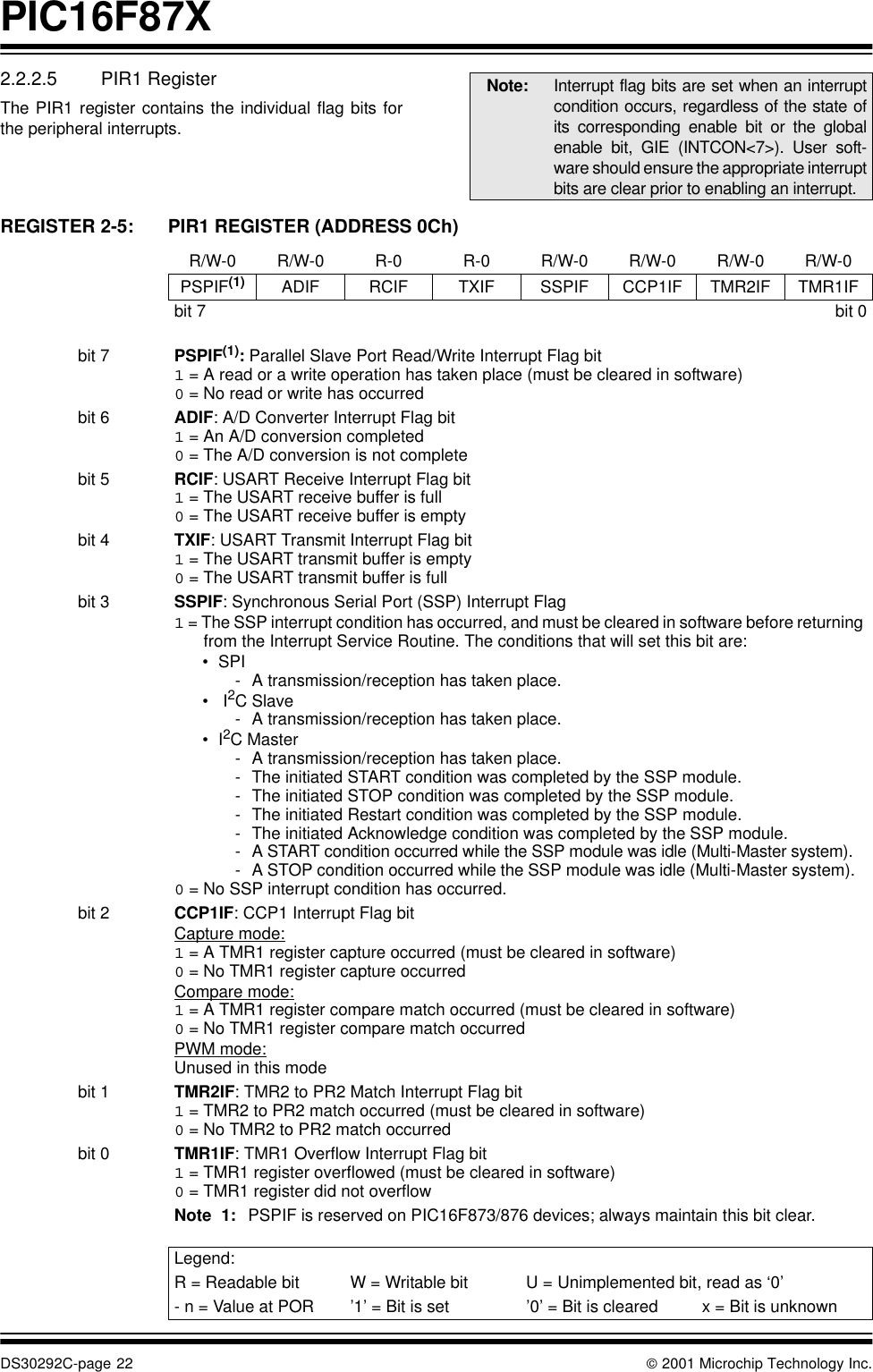
PIC16F87XDS30292C-page 22  2001 Microchip Technology Inc.2.2.2.5 PIR1 RegisterThe PIR1 register contains the individual flag bits forthe peripheral interrupts.Note: Interrupt flag bits are set when an interruptcondition occurs, regardless of the state ofits corresponding enable bit or the globalenable bit, GIE (INTCON<7>). User soft-ware should ensure the appropriate interruptbits are clear prior to enabling an interrupt.REGISTER 2-5: PIR1 REGISTER (ADDRESS 0Ch)  R/W-0 R/W-0 R-0 R-0 R/W-0 R/W-0 R/W-0 R/W-0PSPIF(1) ADIF RCIF TXIF SSPIF CCP1IF TMR2IF TMR1IFbit 7 bit 0bit 7 PSPIF(1): Parallel Slave Port Read/Write Interrupt Flag bit1 = A read or a write operation has taken place (must be cleared in software)0 = No read or write has occurredbit 6 ADIF: A/D Converter Interrupt Flag bit1 = An A/D conversion completed0 = The A/D conversion is not complete bit 5 RCIF: USART Receive Interrupt Flag bit1 = The USART receive buffer is full0 = The USART receive buffer is emptybit 4 TXIF: USART Transmit Interrupt Flag bit1 = The USART transmit buffer is empty0 = The USART transmit buffer is fullbit 3 SSPIF: Synchronous Serial Port (SSP) Interrupt Flag1 = The SSP interrupt condition has occurred, and must be cleared in software before returning from the Interrupt Service Routine. The conditions that will set this bit are:•SPI- A transmission/reception has taken place.• I2C Slave- A transmission/reception has taken place.•I2C Master- A transmission/reception has taken place.- The initiated START condition was completed by the SSP module.- The initiated STOP condition was completed by the SSP module.- The initiated Restart condition was completed by the SSP module.- The initiated Acknowledge condition was completed by the SSP module.- A START condition occurred while the SSP module was idle (Multi-Master system).- A STOP condition occurred while the SSP module was idle (Multi-Master system).0 = No SSP interrupt condition has occurred.bit 2 CCP1IF: CCP1 Interrupt Flag bitCapture mode:1 = A TMR1 register capture occurred (must be cleared in software)0 = No TMR1 register capture occurredCompare mode:1 = A TMR1 register compare match occurred (must be cleared in software)0 = No TMR1 register compare match occurredPWM mode: Unused in this modebit 1 TMR2IF: TMR2 to PR2 Match Interrupt Flag bit1 = TMR2 to PR2 match occurred (must be cleared in software)0 = No TMR2 to PR2 match occurredbit 0 TMR1IF: TMR1 Overflow Interrupt Flag bit1 = TMR1 register overflowed (must be cleared in software)0 = TMR1 register did not overflowNote 1: PSPIF is reserved on PIC16F873/876 devices; always maintain this bit clear.Legend:R = Readable bit W = Writable bit U = Unimplemented bit, read as ‘0’- n = Value at POR ’1’ = Bit is set ’0’ = Bit is cleared x = Bit is unknown
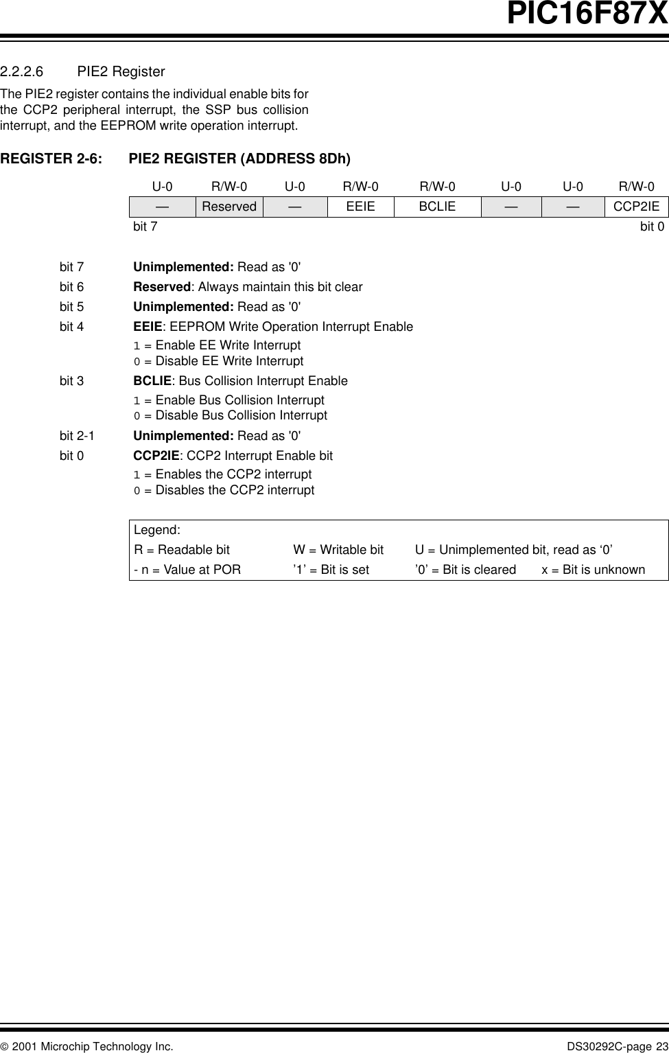
 2001 Microchip Technology Inc. DS30292C-page 23PIC16F87X2.2.2.6 PIE2 RegisterThe PIE2 register contains the individual enable bits forthe CCP2 peripheral interrupt, the SSP bus collisioninterrupt, and the EEPROM write operation interrupt.REGISTER 2-6: PIE2 REGISTER (ADDRESS 8Dh)                      U-0 R/W-0 U-0 R/W-0 R/W-0 U-0 U-0 R/W-0—Reserved —EEIE BCLIE — — CCP2IEbit 7 bit 0bit 7 Unimplemented: Read as '0'bit 6 Reserved: Always maintain this bit clearbit 5 Unimplemented: Read as '0'bit 4 EEIE: EEPROM Write Operation Interrupt Enable1 = Enable EE Write Interrupt0 = Disable EE Write Interruptbit 3 BCLIE: Bus Collision Interrupt Enable1 = Enable Bus Collision Interrupt0 = Disable Bus Collision Interruptbit 2-1 Unimplemented: Read as '0'bit 0 CCP2IE: CCP2 Interrupt Enable bit1 = Enables the CCP2 interrupt0 = Disables the CCP2 interruptLegend:R = Readable bit W = Writable bit U = Unimplemented bit, read as ‘0’- n = Value at POR ’1’ = Bit is set ’0’ = Bit is cleared x = Bit is unknown
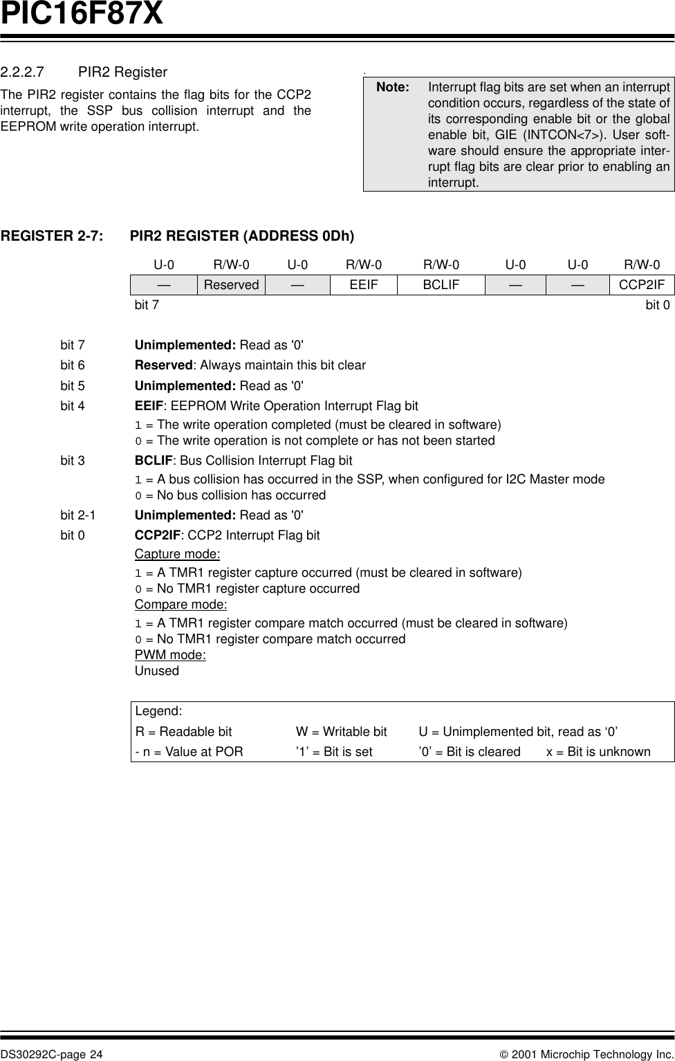
PIC16F87XDS30292C-page 24  2001 Microchip Technology Inc.2.2.2.7 PIR2 RegisterThe PIR2 register contains the flag bits for the CCP2interrupt, the SSP bus collision interrupt and theEEPROM write operation interrupt..REGISTER 2-7: PIR2 REGISTER (ADDRESS 0Dh)                      Note: Interrupt flag bits are set when an interruptcondition occurs, regardless of the state ofits corresponding enable bit or the globalenable bit, GIE (INTCON<7>). User soft-ware should ensure the appropriate inter-rupt flag bits are clear prior to enabling aninterrupt.U-0 R/W-0 U-0 R/W-0 R/W-0 U-0 U-0 R/W-0—Reserved —EEIF BCLIF — — CCP2IFbit 7 bit 0bit 7 Unimplemented: Read as '0'bit 6 Reserved: Always maintain this bit clearbit 5 Unimplemented: Read as '0'bit 4 EEIF: EEPROM Write Operation Interrupt Flag bit1 = The write operation completed (must be cleared in software)0 = The write operation is not complete or has not been startedbit 3 BCLIF: Bus Collision Interrupt Flag bit1 = A bus collision has occurred in the SSP, when configured for I2C Master mode0 = No bus collision has occurredbit 2-1 Unimplemented: Read as '0'bit 0 CCP2IF: CCP2 Interrupt Flag bitCapture mode:1 = A TMR1 register capture occurred (must be cleared in software)0 = No TMR1 register capture occurredCompare mode:1 = A TMR1 register compare match occurred (must be cleared in software)0 = No TMR1 register compare match occurredPWM mode: UnusedLegend:R = Readable bit W = Writable bit U = Unimplemented bit, read as ‘0’- n = Value at POR ’1’ = Bit is set ’0’ = Bit is cleared x = Bit is unknown
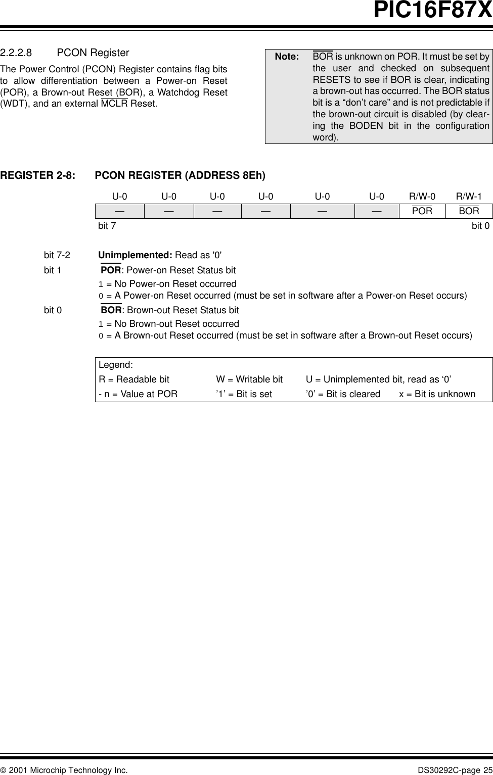
 2001 Microchip Technology Inc. DS30292C-page 25PIC16F87X2.2.2.8 PCON RegisterThe Power Control (PCON) Register contains flag bitsto allow differentiation between a Power-on Reset(POR), a Brown-out Reset (BOR), a Watchdog Reset(WDT), and an external MCLR Reset. REGISTER 2-8: PCON REGISTER (ADDRESS 8Eh)                      Note: BOR is unknown on POR. It must be set bythe user and checked on subsequentRESETS to see if BOR is clear, indicatinga brown-out has occurred. The BOR statusbit is a “don’t care” and is not predictable ifthe brown-out circuit is disabled (by clear-ing the BODEN bit in the configurationword).U-0 U-0 U-0 U-0 U-0 U-0 R/W-0 R/W-1— — — — — —PORBORbit 7 bit 0bit 7-2 Unimplemented: Read as '0'bit 1  POR: Power-on Reset Status bit1 = No Power-on Reset occurred0 = A Power-on Reset occurred (must be set in software after a Power-on Reset occurs)bit 0  BOR: Brown-out Reset Status bit1 = No Brown-out Reset occurred0 = A Brown-out Reset occurred (must be set in software after a Brown-out Reset occurs)Legend:R = Readable bit W = Writable bit U = Unimplemented bit, read as ‘0’- n = Value at POR ’1’ = Bit is set ’0’ = Bit is cleared x = Bit is unknown
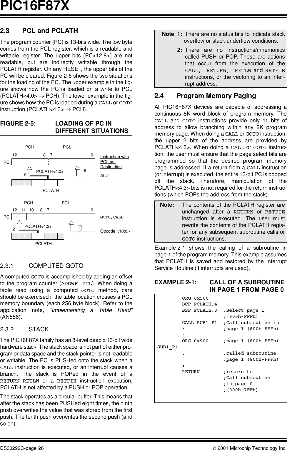
PIC16F87XDS30292C-page 26  2001 Microchip Technology Inc.2.3 PCL and PCLATHThe program counter (PC) is 13-bits wide. The low bytecomes from the PCL register, which is a readable andwritable register. The upper bits (PC<12:8>) are notreadable, but are indirectly writable through thePCLATH register. On any RESET, the upper bits of thePC will be cleared. Figure 2-5 shows the two situationsfor the loading of the PC. The upper example in the fig-ure shows how the PC is loaded on a write to PCL(PCLATH<4:0> → PCH). The lower example in the fig-ure shows how the PC is loaded during a CALL or GOTOinstruction (PCLATH<4:3> → PCH).FIGURE 2-5: LOADING OF PC IN DIFFERENT SITUATIONS2.3.1 COMPUTED GOTOA computed GOTO is accomplished by adding an offsetto the program counter (ADDWF PCL). When doing atable read using a computed GOTO method, careshould be exercised if the table location crosses a PCLmemory boundary (each 256 byte block). Refer to theapplication note, “Implementing a Table Read"(AN556).2.3.2 STACKThe PIC16F87X family has an 8-level deep x 13-bit widehardware stack. The stack space is not part of either pro-gram or data space and the stack pointer is not readableor writable. The PC is PUSHed onto the stack when aCALL instruction is executed, or an interrupt causes abranch. The stack is POPed in the event of aRETURN,RETLW or a RETFIE instruction execution.PCLATH is not affected by a PUSH or POP operation.The stack operates as a circular buffer. This means thatafter the stack has been PUSHed eight times, the ninthpush overwrites the value that was stored from the firstpush. The tenth push overwrites the second push (andso on). 2.4 Program Memory PagingAll PIC16F87X devices are capable of addressing acontinuous 8K word block of program memory. TheCALL and GOTO instructions provide only 11 bits ofaddress to allow branching within any 2K programmemory page. When doing a CALL or GOTO instruction,the upper 2 bits of the address are provided byPCLATH<4:3>. When doing a CALL or GOTO instruc-tion, the user must ensure that the page select bits areprogrammed so that the desired program memorypage is addressed. If a return from a CALL instruction(or interrupt) is executed, the entire 13-bit PC is poppedoff the stack. Therefore, manipulation of thePCLATH<4:3> bits is not required for the return instruc-tions (which POPs the address from the stack).Example 2-1 shows the calling of a subroutine inpage 1 of the program memory. This example assumesthat PCLATH is saved and restored by the InterruptService Routine (if interrupts are used).EXAMPLE 2-1: CALL OF A SUBROUTINE IN PAGE 1 FROM PAGE 0PC12 8 7 05PCLATH<4:0>PCLATHInstruction withALUGOTO,CALLOpcode <10:0>8PC12 11 10 011PCLATH<4:3>PCH PCL872PCLATHPCH PCLPCL as DestinationNote 1: There are no status bits to indicate stackoverflow or stack underflow conditions.2: There are no instructions/mnemonicscalled PUSH or POP. These are actionsthat occur from the execution of theCALL, RETURN, RETLW and RETFIEinstructions, or the vectoring to an inter-rupt address.Note: The contents of the PCLATH register areunchanged after a RETURN or RETFIEinstruction is executed. The user mustrewrite the contents of the PCLATH regis-ter for any subsequent subroutine calls orGOTO instructions.ORG 0x500BCF PCLATH,4BSF PCLATH,3 ;Select page 1;(800h-FFFh)CALL SUB1_P1 ;Call subroutine in: ;page 1 (800h-FFFh):ORG 0x900 ;page 1 (800h-FFFh)SUB1_P1: ;called subroutine;page 1 (800h-FFFh):RETURN ;return to ;Call subroutine  ;in page 0;(000h-7FFh)
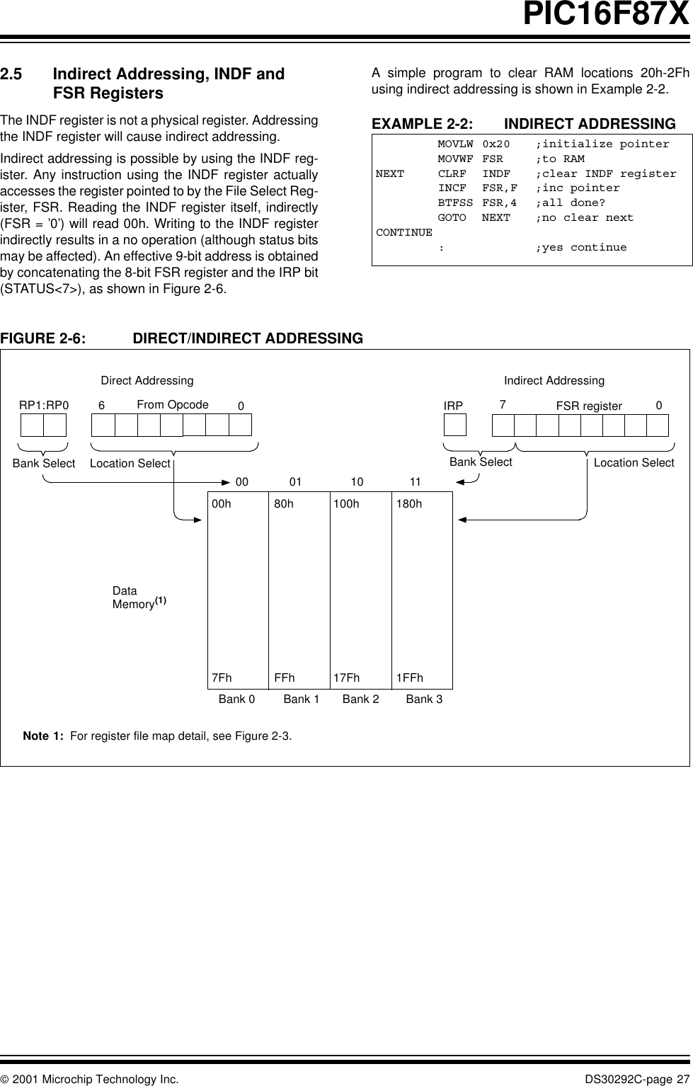
 2001 Microchip Technology Inc. DS30292C-page 27PIC16F87X2.5 Indirect Addressing, INDF and FSR RegistersThe INDF register is not a physical register. Addressingthe INDF register will cause indirect addressing. Indirect addressing is possible by using the INDF reg-ister. Any instruction using the INDF register actuallyaccesses the register pointed to by the File Select Reg-ister, FSR. Reading the INDF register itself, indirectly(FSR = ’0’) will read 00h. Writing to the INDF registerindirectly results in a no operation (although status bitsmay be affected). An effective 9-bit address is obtainedby concatenating the 8-bit FSR register and the IRP bit(STATUS<7>), as shown in Figure 2-6.A simple program to clear RAM locations 20h-2Fhusing indirect addressing is shown in Example 2-2.EXAMPLE 2-2: INDIRECT ADDRESSINGFIGURE 2-6: DIRECT/INDIRECT ADDRESSINGMOVLW 0x20 ;initialize pointerMOVWF FSR ;to RAMNEXT CLRF INDF ;clear INDF registerINCF FSR,F ;inc pointerBTFSS FSR,4 ;all done? GOTO NEXT ;no clear nextCONTINUE: ;yes continueNote 1: For register file map detail, see Figure 2-3.DataMemory(1)Indirect AddressingDirect AddressingBank Select Location SelectRP1:RP0 6 0From Opcode IRP FSR register70Bank Select Location Select00 01 10 11Bank 0 Bank 1 Bank 2 Bank 3FFh80h7Fh00h17Fh100h1FFh180h
PIC16F87XDS30292C-page 28  2001 Microchip Technology Inc.NOTES:
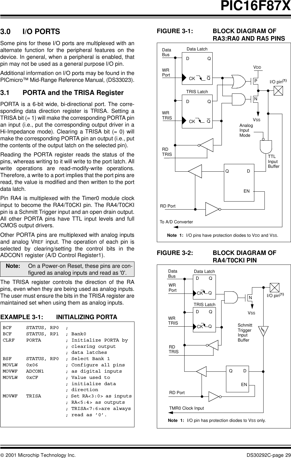
 2001 Microchip Technology Inc. DS30292C-page 29PIC16F87X3.0 I/O PORTSSome pins for these I/O ports are multiplexed with analternate function for the peripheral features on thedevice. In general, when a peripheral is enabled, thatpin may not be used as a general purpose I/O pin.Additional information on I/O ports may be found in thePICmicro™ Mid-Range Reference Manual, (DS33023).3.1 PORTA and the TRISA RegisterPORTA is a 6-bit wide, bi-directional port. The corre-sponding data direction register is TRISA. Setting aTRISA bit (= 1) will make the corresponding PORTA pinan input (i.e., put the corresponding output driver in aHi-Impedance mode). Clearing a TRISA bit (= 0) willmake the corresponding PORTA pin an output (i.e., putthe contents of the output latch on the selected pin).Reading the PORTA register reads the status of thepins, whereas writing to it will write to the port latch. Allwrite operations are read-modify-write operations.Therefore, a write to a port implies that the port pins areread, the value is modified and then written to the portdata latch.Pin RA4 is multiplexed with the Timer0 module clockinput to become the RA4/T0CKI pin. The RA4/T0CKIpin is a Schmitt Trigger input and an open drain output.All other PORTA pins have TTL input levels and fullCMOS output drivers.Other PORTA pins are multiplexed with analog inputsand analog VREF input. The operation of each pin isselected by clearing/setting the control bits in theADCON1 register (A/D Control Register1).   The TRISA register controls the direction of the RApins, even when they are being used as analog inputs.The user must ensure the bits in the TRISA register aremaintained set when using them as analog inputs. EXAMPLE 3-1: INITIALIZING PORTAFIGURE 3-1: BLOCK DIAGRAM OF RA3:RA0 AND RA5 PINS  FIGURE 3-2: BLOCK DIAGRAM OF RA4/T0CKI PIN    Note: On a Power-on Reset, these pins are con-figured as analog inputs and read as '0'.BCF STATUS, RP0 ;BCF STATUS, RP1 ; Bank0CLRF PORTA ; Initialize PORTA by; clearing output; data latchesBSF STATUS, RP0 ; Select Bank 1MOVLW 0x06 ; Configure all pinsMOVWF ADCON1 ; as digital inputsMOVLW 0xCF ; Value used to ; initialize data ; directionMOVWF TRISA ; Set RA<3:0> as inputs; RA<5:4> as outputs; TRISA<7:6>are always; read as ’0’.DataBusQDQCKQDQCKQDENPNWRPortWRTRISData LatchTRIS LatchRD RD PortVSSVDDI/O pin(1)Note 1: I/O pins have protection diodes to VDD and VSS.AnalogInputModeTTLInputBufferTo A/D ConverterTRISDataBusWRPortWRTRISRD PortData LatchTRIS LatchRD SchmittTriggerInputBufferNVSSI/O pin(1)TMR0 Clock InputQDQCKQDQCKENQDENNote 1: I/O pin has protection diodes to VSS only.TRIS
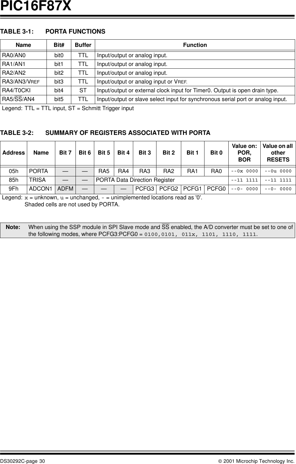
PIC16F87XDS30292C-page 30  2001 Microchip Technology Inc.TABLE 3-1: PORTA FUNCTIONSTABLE 3-2: SUMMARY OF REGISTERS ASSOCIATED WITH PORTAName Bit# Buffer FunctionRA0/AN0 bit0 TTL Input/output or analog input.RA1/AN1 bit1 TTL Input/output or analog input.RA2/AN2 bit2 TTL Input/output or analog input.RA3/AN3/VREF bit3 TTL Input/output or analog input or VREF.RA4/T0CKI bit4 ST Input/output or external clock input for Timer0. Output is open drain type.RA5/SS/AN4 bit5 TTL Input/output or slave select input for synchronous serial port or analog input.Legend: TTL = TTL input, ST = Schmitt Trigger inputAddress Name Bit 7 Bit 6 Bit 5 Bit 4 Bit 3 Bit 2 Bit 1 Bit 0 Value on: POR,BORValue on all other RESETS05h PORTA — — RA5 RA4 RA3 RA2 RA1 RA0 --0x 0000 --0u 000085h TRISA — — PORTA Data Direction Register --11 1111 --11 11119Fh ADCON1 ADFM — — — PCFG3 PCFG2 PCFG1 PCFG0 --0- 0000 --0- 0000Legend: x = unknown, u = unchanged, - = unimplemented locations read as '0'. Shaded cells are not used by PORTA.Note: When using the SSP module in SPI Slave mode and SS enabled, the A/D converter must be set to one ofthe following modes, where PCFG3:PCFG0 = 0100,0101, 011x, 1101, 1110, 1111.
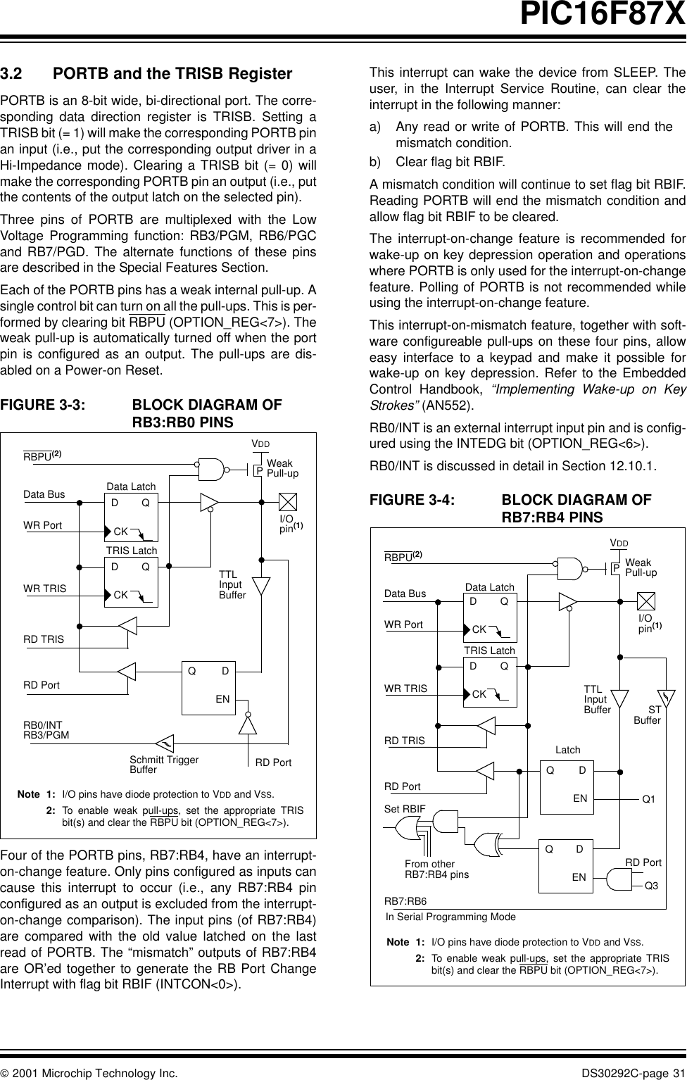
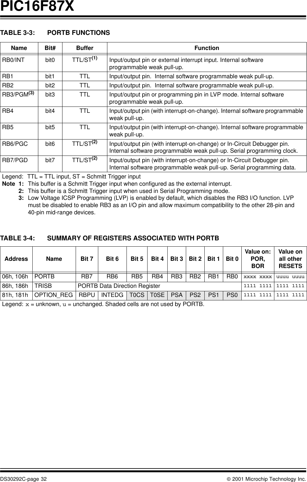
 2001 Microchip Technology Inc. DS30292C-page 31PIC16F87X3.2 PORTB and the TRISB RegisterPORTB is an 8-bit wide, bi-directional port. The corre-sponding data direction register is TRISB. Setting aTRISB bit (= 1) will make the corresponding PORTB pinan input (i.e., put the corresponding output driver in aHi-Impedance mode). Clearing a TRISB bit (= 0) willmake the corresponding PORTB pin an output (i.e., putthe contents of the output latch on the selected pin).Three pins of PORTB are multiplexed with the LowVoltage Programming function: RB3/PGM, RB6/PGCand RB7/PGD. The alternate functions of these pinsare described in the Special Features Section.Each of the PORTB pins has a weak internal pull-up. Asingle control bit can turn on all the pull-ups. This is per-formed by clearing bit RBPU (OPTION_REG<7>). Theweak pull-up is automatically turned off when the portpin is configured as an output. The pull-ups are dis-abled on a Power-on Reset.FIGURE 3-3: BLOCK DIAGRAM OF RB3:RB0 PINS Four of the PORTB pins, RB7:RB4, have an interrupt-on-change feature. Only pins configured as inputs cancause this interrupt to occur (i.e., any RB7:RB4 pinconfigured as an output is excluded from the interrupt-on-change comparison). The input pins (of RB7:RB4)are compared with the old value latched on the lastread of PORTB. The “mismatch” outputs of RB7:RB4are OR’ed together to generate the RB Port ChangeInterrupt with flag bit RBIF (INTCON<0>). This interrupt can wake the device from SLEEP. Theuser, in the Interrupt Service Routine, can clear theinterrupt in the following manner:a) Any read or write of PORTB. This will end themismatch condition.b) Clear flag bit RBIF.A mismatch condition will continue to set flag bit RBIF.Reading PORTB will end the mismatch condition andallow flag bit RBIF to be cleared.The interrupt-on-change feature is recommended forwake-up on key depression operation and operationswhere PORTB is only used for the interrupt-on-changefeature. Polling of PORTB is not recommended whileusing the interrupt-on-change feature.This interrupt-on-mismatch feature, together with soft-ware configureable pull-ups on these four pins, alloweasy interface to a keypad and make it possible forwake-up on key depression. Refer to the EmbeddedControl Handbook, “Implementing Wake-up on KeyStrokes” (AN552).RB0/INT is an external interrupt input pin and is config-ured using the INTEDG bit (OPTION_REG<6>).RB0/INT is discussed in detail in Section 12.10.1. FIGURE 3-4: BLOCK DIAGRAM OFRB7:RB4 PINS Data LatchRBPU(2)PVDDQDCKQDCKQDENData BusWR PortWR TRISRD TRISRD PortWeakPull-upRD PortRB0/INTI/Opin(1)TTLInputBufferSchmitt TriggerBufferTRIS LatchNote 1: I/O pins have diode protection to VDD and VSS.2: To enable weak pull-ups, set the appropriate TRISbit(s) and clear the RBPU bit (OPTION_REG<7>).RB3/PGMData LatchFrom otherRBPU(2)PVDDI/OQDCKQDCKQDENQDENData BusWR PortWR TRISSet RBIFTRIS LatchRD TRISRD PortRB7:RB4 pinsWeakPull-upRD PortLatchTTLInputBufferpin(1)STBufferRB7:RB6 Q3Q1Note 1: I/O pins have diode protection to VDD and VSS.2: To enable weak pull-ups, set the appropriate TRISbit(s) and clear the RBPU bit (OPTION_REG<7>).In Serial Programming Mode
PIC16F87XDS30292C-page 32  2001 Microchip Technology Inc.TABLE 3-3: PORTB FUNCTIONSTABLE 3-4: SUMMARY OF REGISTERS ASSOCIATED WITH PORTBName Bit# Buffer FunctionRB0/INT bit0 TTL/ST(1) Input/output pin or external interrupt input. Internal software programmable weak pull-up.RB1 bit1 TTL Input/output pin.  Internal software programmable weak pull-up.RB2 bit2 TTL Input/output pin.  Internal software programmable weak pull-up.RB3/PGM(3) bit3 TTL Input/output pin or programming pin in LVP mode. Internal software programmable weak pull-up.RB4 bit4 TTL Input/output pin (with interrupt-on-change). Internal software programmable weak pull-up.RB5 bit5 TTL Input/output pin (with interrupt-on-change). Internal software programmable weak pull-up.RB6/PGC bit6 TTL/ST(2) Input/output pin (with interrupt-on-change) or In-Circuit Debugger pin. Internal software programmable weak pull-up. Serial programming clock.RB7/PGD bit7 TTL/ST(2) Input/output pin (with interrupt-on-change) or In-Circuit Debugger pin. Internal software programmable weak pull-up. Serial programming data.Legend:  TTL = TTL input, ST = Schmitt Trigger inputNote 1: This buffer is a Schmitt Trigger input when configured as the external interrupt.2: This buffer is a Schmitt Trigger input when used in Serial Programming mode.3: Low Voltage ICSP Programming (LVP) is enabled by default, which disables the RB3 I/O function. LVP must be disabled to enable RB3 as an I/O pin and allow maximum compatibility to the other 28-pin and 40-pin mid-range devices.Address Name Bit 7 Bit 6 Bit 5 Bit 4 Bit 3 Bit 2 Bit 1 Bit 0 Value on: POR,BORValue on all other RESETS06h, 106h PORTB RB7 RB6 RB5 RB4 RB3 RB2 RB1 RB0 xxxx xxxx uuuu uuuu86h, 186h TRISB PORTB Data Direction Register 1111 1111 1111 111181h, 181h OPTION_REG RBPU INTEDG T0CS T0SE PSA PS2 PS1 PS0 1111 1111 1111 1111Legend: x = unknown, u = unchanged. Shaded cells are not used by PORTB.
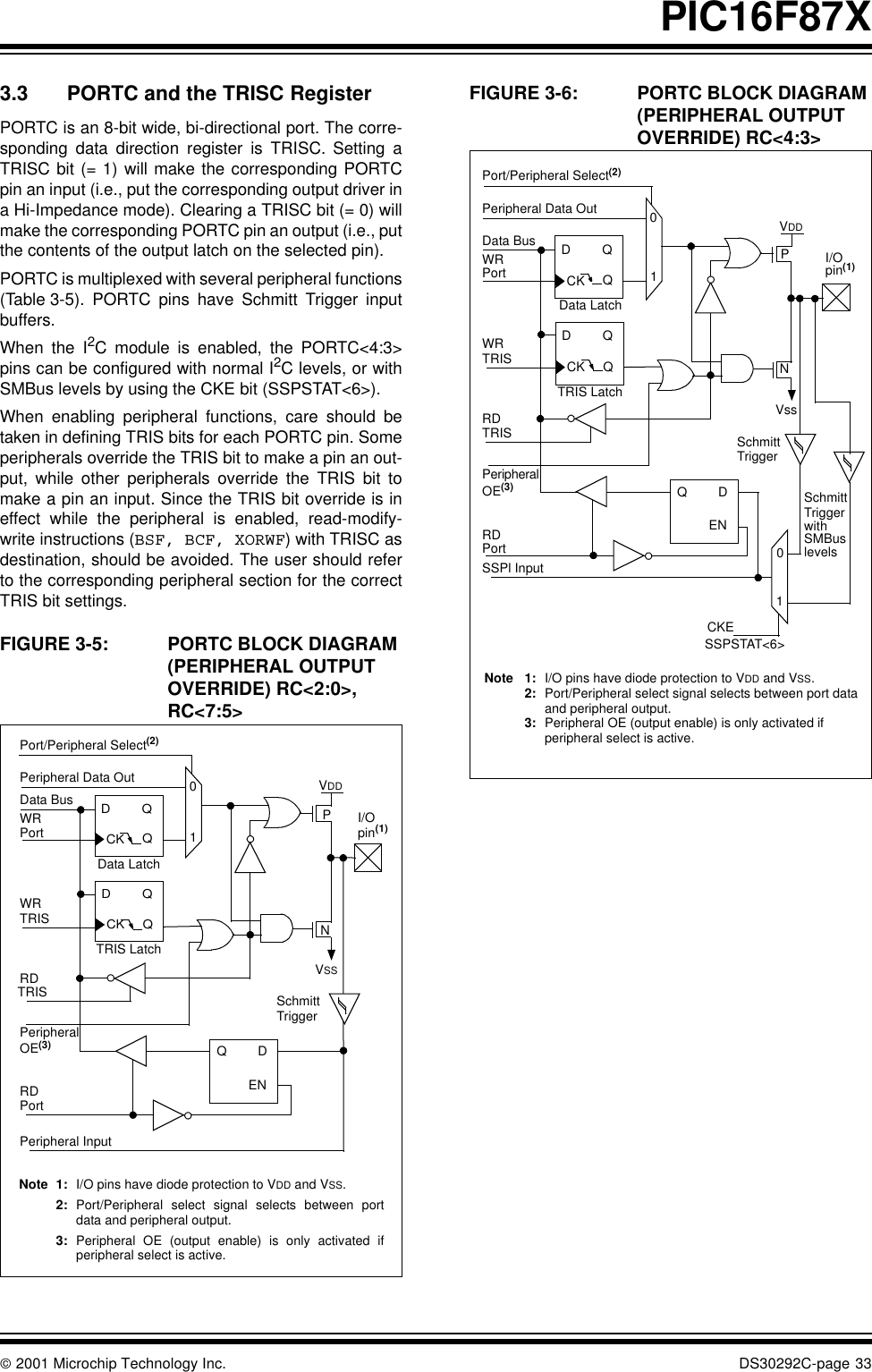
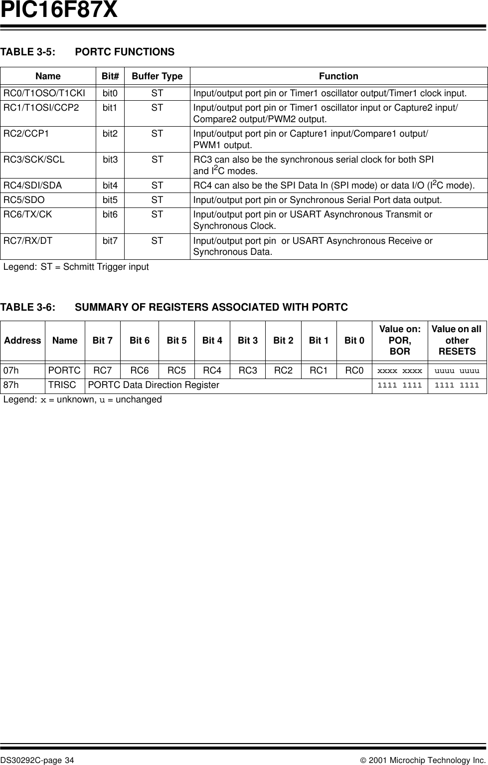
 2001 Microchip Technology Inc. DS30292C-page 33PIC16F87X3.3 PORTC and the TRISC RegisterPORTC is an 8-bit wide, bi-directional port. The corre-sponding data direction register is TRISC. Setting aTRISC bit (= 1) will make the corresponding PORTCpin an input (i.e., put the corresponding output driver ina Hi-Impedance mode). Clearing a TRISC bit (= 0) willmake the corresponding PORTC pin an output (i.e., putthe contents of the output latch on the selected pin).PORTC is multiplexed with several peripheral functions(Table 3-5). PORTC pins have Schmitt Trigger inputbuffers.When the I2C module is enabled, the PORTC<4:3>pins can be configured with normal I2C levels, or withSMBus levels by using the CKE bit (SSPSTAT<6>).When enabling peripheral functions, care should betaken in defining TRIS bits for each PORTC pin. Someperipherals override the TRIS bit to make a pin an out-put, while other peripherals override the TRIS bit tomake a pin an input. Since the TRIS bit override is ineffect while the peripheral is enabled, read-modify-write instructions (BSF, BCF, XORWF) with TRISC asdestination, should be avoided. The user should referto the corresponding peripheral section for the correctTRIS bit settings.FIGURE 3-5: PORTC BLOCK DIAGRAM (PERIPHERAL OUTPUT OVERRIDE) RC<2:0>, RC<7:5> FIGURE 3-6: PORTC BLOCK DIAGRAM (PERIPHERAL OUTPUT OVERRIDE) RC<4:3>Port/Peripheral Select(2)Data BusWRPortWRTRISRD Data LatchTRIS LatchRD SchmittTriggerQDQCKQDENPeripheral Data Out 01QDQCKPNVDDVSSPortPeripheralOE(3)Peripheral InputI/Opin(1)Note 1: I/O pins have diode protection to VDD and VSS.2: Port/Peripheral select signal selects between portdata and peripheral output.3: Peripheral OE (output enable) is only activated ifperipheral select is active.TRISPort/Peripheral Select(2)Data BusWRPortWRTRISRD Data LatchTRIS LatchRD SchmittTriggerQDQCKQDENPeripheral Data Out 01QDQCKPNVDDVssPortPeripheralOE(3)SSPl InputI/Opin(1)Note 1: I/O pins have diode protection to VDD and VSS.2: Port/Peripheral select signal selects between port data and peripheral output.3: Peripheral OE (output enable) is only activated if peripheral select is active.01CKESSPSTAT<6>SchmittTriggerwithSMBuslevelsTRIS
PIC16F87XDS30292C-page 34  2001 Microchip Technology Inc.TABLE 3-5: PORTC FUNCTIONS TABLE 3-6: SUMMARY OF REGISTERS ASSOCIATED WITH PORTCName Bit# Buffer Type FunctionRC0/T1OSO/T1CKI bit0 ST Input/output port pin or Timer1 oscillator output/Timer1 clock input.RC1/T1OSI/CCP2 bit1 ST Input/output port pin or Timer1 oscillator input or Capture2 input/Compare2 output/PWM2 output.RC2/CCP1 bit2 ST Input/output port pin or Capture1 input/Compare1 output/PWM1 output.RC3/SCK/SCL bit3 ST RC3 can also be the synchronous serial clock for both SPI and I2C modes.RC4/SDI/SDA bit4 ST RC4 can also be the SPI Data In (SPI mode) or data I/O (I2C mode).RC5/SDO bit5 ST Input/output port pin or Synchronous Serial Port data output.RC6/TX/CK bit6 ST Input/output port pin or USART Asynchronous Transmit or Synchronous Clock.RC7/RX/DT bit7 ST Input/output port pin  or USART Asynchronous Receive or Synchronous Data.Legend: ST = Schmitt Trigger inputAddress Name Bit 7 Bit 6 Bit 5 Bit 4 Bit 3 Bit 2 Bit 1 Bit 0 Value on: POR,BORValue on all other RESETS07h PORTC RC7 RC6 RC5 RC4 RC3 RC2 RC1 RC0 xxxx xxxx uuuu uuuu87h TRISC PORTC Data Direction Register 1111 1111 1111 1111Legend: x = unknown, u = unchanged
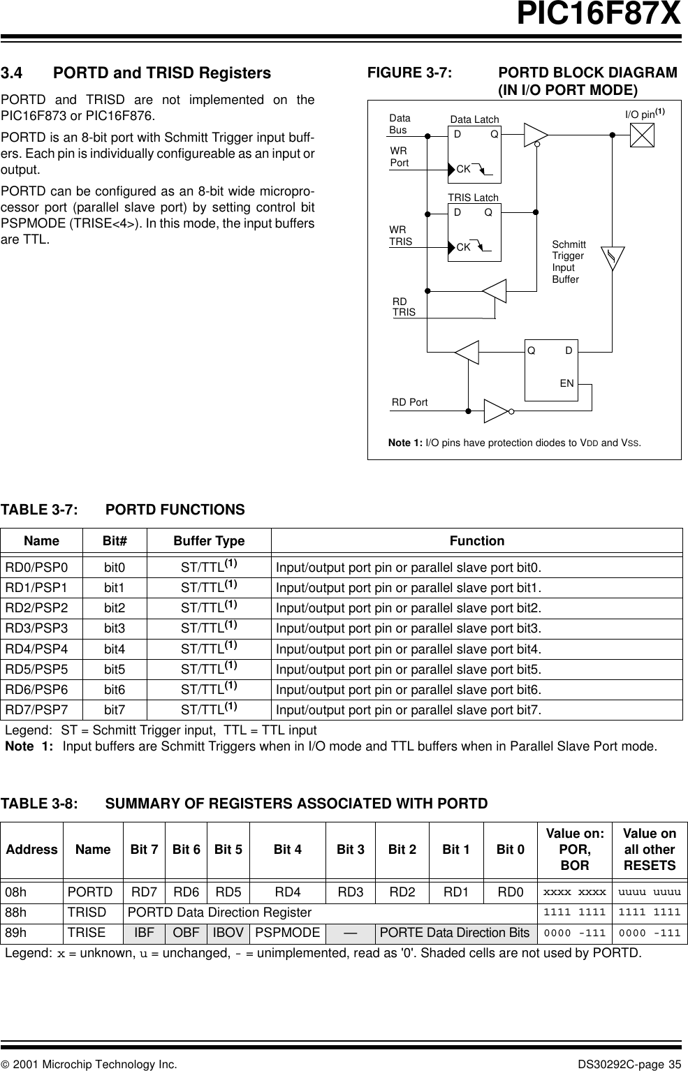
 2001 Microchip Technology Inc. DS30292C-page 35PIC16F87X3.4 PORTD and TRISD RegistersPORTD and TRISD are not implemented on thePIC16F873 or PIC16F876.PORTD is an 8-bit port with Schmitt Trigger input buff-ers. Each pin is individually configureable as an input oroutput.PORTD can be configured as an 8-bit wide micropro-cessor port (parallel slave port) by setting control bitPSPMODE (TRISE<4>). In this mode, the input buffersare TTL.FIGURE 3-7: PORTD BLOCK DIAGRAM (IN I/O PORT MODE)  TABLE 3-7: PORTD FUNCTIONSTABLE 3-8: SUMMARY OF REGISTERS ASSOCIATED WITH PORTDDataBusWRPortWRTRISRD PortData LatchTRIS LatchRD SchmittTriggerInputBufferI/O pin(1)Note 1: I/O pins have protection diodes to VDD and VSS.QDCKQDCKENQDENTRISName Bit# Buffer Type FunctionRD0/PSP0 bit0 ST/TTL(1) Input/output port pin or parallel slave port bit0.RD1/PSP1 bit1 ST/TTL(1) Input/output port pin or parallel slave port bit1.RD2/PSP2 bit2 ST/TTL(1) Input/output port pin or parallel slave port bit2.RD3/PSP3 bit3 ST/TTL(1) Input/output port pin or parallel slave port bit3.RD4/PSP4 bit4 ST/TTL(1) Input/output port pin or parallel slave port bit4.RD5/PSP5 bit5 ST/TTL(1) Input/output port pin or parallel slave port bit5.RD6/PSP6 bit6 ST/TTL(1) Input/output port pin or parallel slave port bit6.RD7/PSP7 bit7 ST/TTL(1) Input/output port pin or parallel slave port bit7.Legend:  ST = Schmitt Trigger input,  TTL = TTL input Note 1: Input buffers are Schmitt Triggers when in I/O mode and TTL buffers when in Parallel Slave Port mode.Address Name Bit 7 Bit 6 Bit 5 Bit 4 Bit 3 Bit 2 Bit 1 Bit 0 Value on:POR,BORValue on all other RESETS08h PORTD RD7 RD6 RD5 RD4 RD3 RD2 RD1 RD0 xxxx xxxx uuuu uuuu88h TRISD PORTD Data Direction Register 1111 1111 1111 111189h TRISE IBF OBF IBOV PSPMODE —PORTE Data Direction Bits 0000 -111 0000 -111Legend: x = unknown, u = unchanged, - = unimplemented, read as '0'. Shaded cells are not used by PORTD.
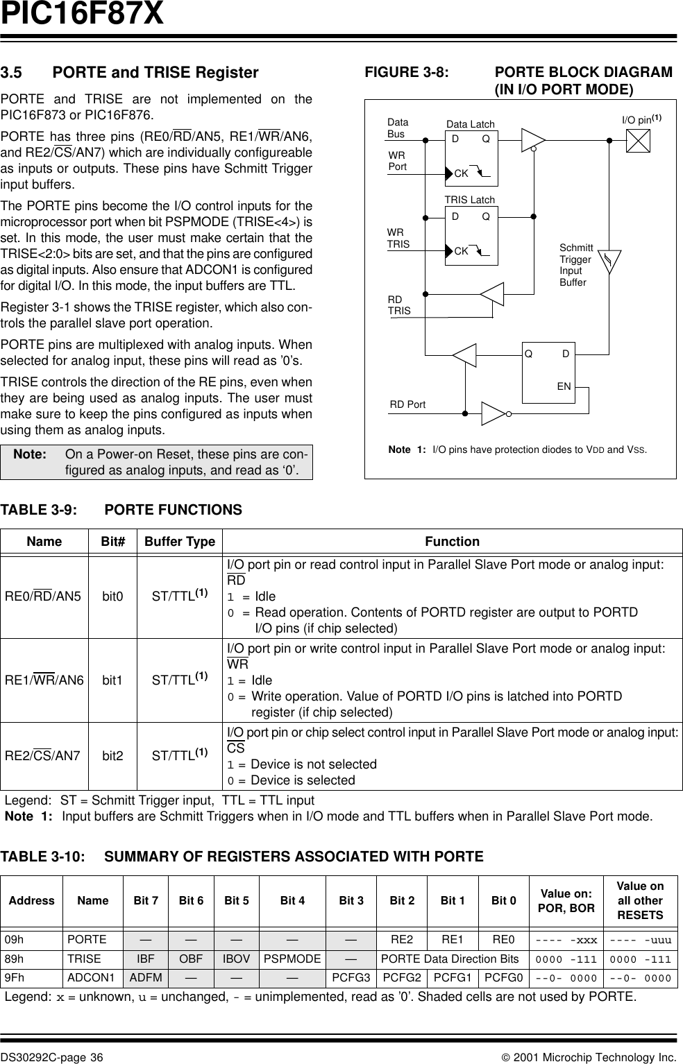
PIC16F87XDS30292C-page 36  2001 Microchip Technology Inc.3.5 PORTE and TRISE RegisterPORTE and TRISE are not implemented on thePIC16F873 or PIC16F876. PORTE has three pins (RE0/RD/AN5, RE1/WR/AN6,and RE2/CS/AN7) which are individually configureableas inputs or outputs. These pins have Schmitt Triggerinput buffers.The PORTE pins become the I/O control inputs for themicroprocessor port when bit PSPMODE (TRISE<4>) isset. In this mode, the user must make certain that theTRISE<2:0> bits are set, and that the pins are configuredas digital inputs. Also ensure that ADCON1 is configuredfor digital I/O. In this mode, the input buffers are TTL.Register 3-1 shows the TRISE register, which also con-trols the parallel slave port operation. PORTE pins are multiplexed with analog inputs. Whenselected for analog input, these pins will read as ’0’s.TRISE controls the direction of the RE pins, even whenthey are being used as analog inputs. The user mustmake sure to keep the pins configured as inputs whenusing them as analog inputs.FIGURE 3-8: PORTE BLOCK DIAGRAM (IN I/O PORT MODE)  TABLE 3-9: PORTE FUNCTIONSTABLE 3-10: SUMMARY OF REGISTERS ASSOCIATED WITH PORTENote: On a Power-on Reset, these pins are con-figured as analog inputs, and read as ‘0’.DataBusWRPortWRTRISRD PortData LatchTRIS LatchRD SchmittTriggerInputBufferQDCKQDCKENQDENI/O pin(1)Note 1: I/O pins have protection diodes to VDD and VSS.TRISName Bit# Buffer Type FunctionRE0/RD/AN5 bit0 ST/TTL(1)I/O port pin or read control input in Parallel Slave Port mode or analog input:RD1 =Idle0 = Read operation. Contents of PORTD register are output to PORTD I/O pins (if chip selected)RE1/WR/AN6 bit1 ST/TTL(1)I/O port pin or write control input in Parallel Slave Port mode or analog input:WR1 =Idle0 = Write operation. Value of PORTD I/O pins is latched into PORTD register (if chip selected)RE2/CS/AN7 bit2 ST/TTL(1)I/O port pin or chip select control input in Parallel Slave Port mode or analog input:CS1 = Device is not selected0 = Device is selectedLegend:  ST = Schmitt Trigger input,  TTL = TTL input Note 1: Input buffers are Schmitt Triggers when in I/O mode and TTL buffers when in Parallel Slave Port mode.Address Name Bit 7 Bit 6 Bit 5 Bit 4 Bit 3 Bit 2 Bit 1 Bit 0 Value on: POR, BORValue on all other RESETS09h PORTE — — — — — RE2 RE1 RE0 ---- -xxx ---- -uuu89h TRISE IBF OBF IBOV PSPMODE —PORTE Data Direction Bits 0000 -111 0000 -1119Fh ADCON1 ADFM — — — PCFG3 PCFG2 PCFG1 PCFG0 --0- 0000 --0- 0000Legend: x = unknown, u = unchanged, - = unimplemented, read as ’0’. Shaded cells are not used by PORTE.
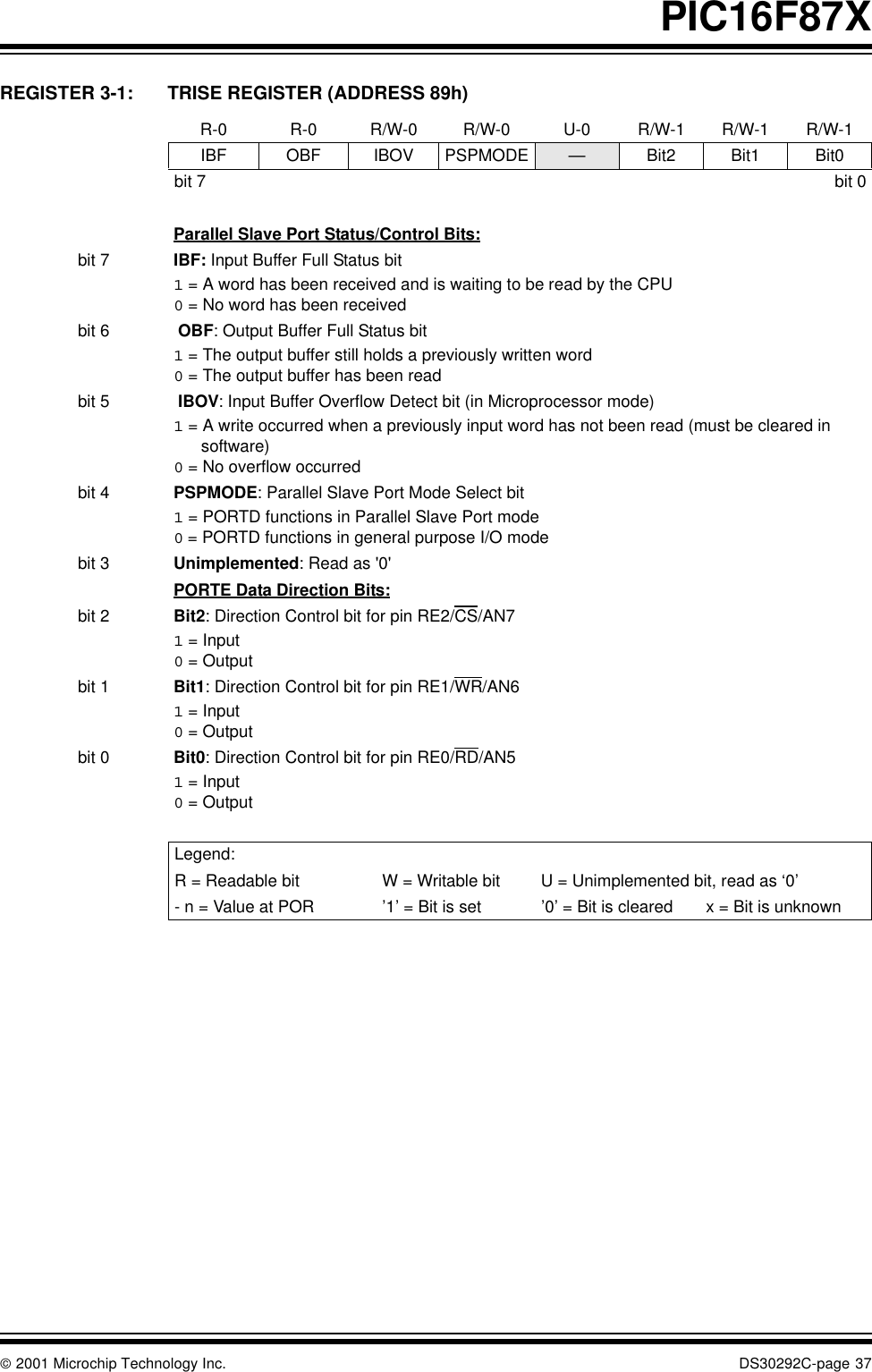
 2001 Microchip Technology Inc. DS30292C-page 37PIC16F87XREGISTER 3-1: TRISE REGISTER (ADDRESS 89h)                 R-0 R-0 R/W-0 R/W-0 U-0 R/W-1 R/W-1 R/W-1IBF OBF IBOV PSPMODE —Bit2 Bit1 Bit0bit 7 bit 0Parallel Slave Port Status/Control Bits:bit 7 IBF: Input Buffer Full Status bit1 = A word has been received and is waiting to be read by the CPU0 = No word has been receivedbit 6  OBF: Output Buffer Full Status bit1 = The output buffer still holds a previously written word0 = The output buffer has been readbit 5  IBOV: Input Buffer Overflow Detect bit (in Microprocessor mode)1 = A write occurred when a previously input word has not been read (must be cleared in software)0 = No overflow occurredbit 4 PSPMODE: Parallel Slave Port Mode Select bit1 = PORTD functions in Parallel Slave Port mode0= PORTD functions in general purpose I/O modebit 3 Unimplemented: Read as '0'PORTE Data Direction Bits:bit 2 Bit2: Direction Control bit for pin RE2/CS/AN71 = Input0 = Outputbit 1 Bit1: Direction Control bit for pin RE1/WR/AN61 = Input0 = Outputbit 0 Bit0: Direction Control bit for pin RE0/RD/AN51 = Input0 = OutputLegend:R = Readable bit W = Writable bit U = Unimplemented bit, read as ‘0’- n = Value at POR ’1’ = Bit is set ’0’ = Bit is cleared x = Bit is unknown
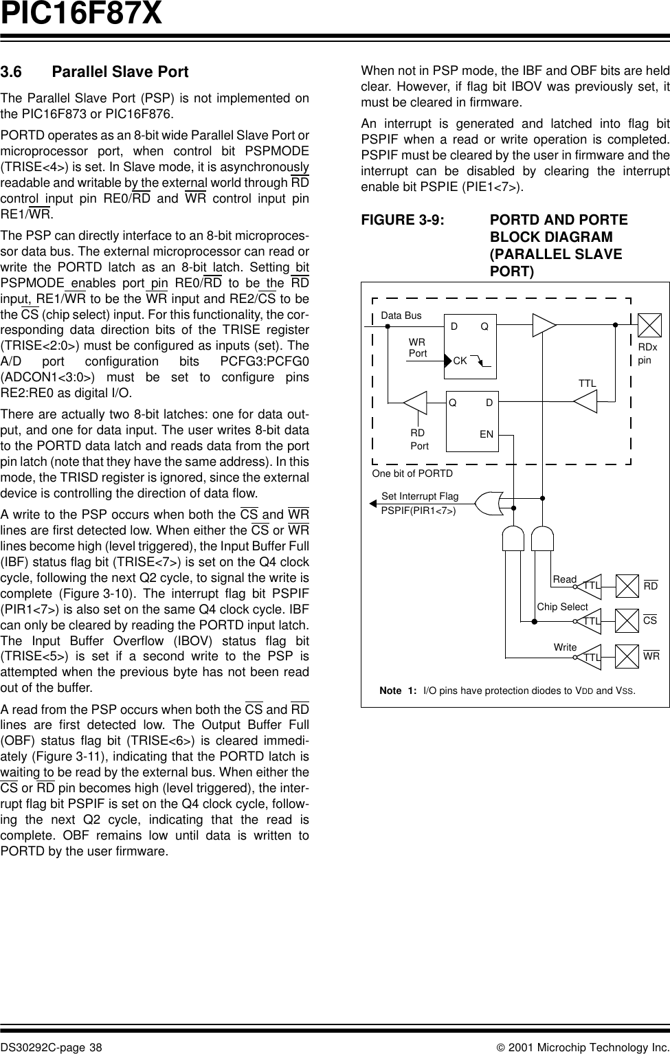
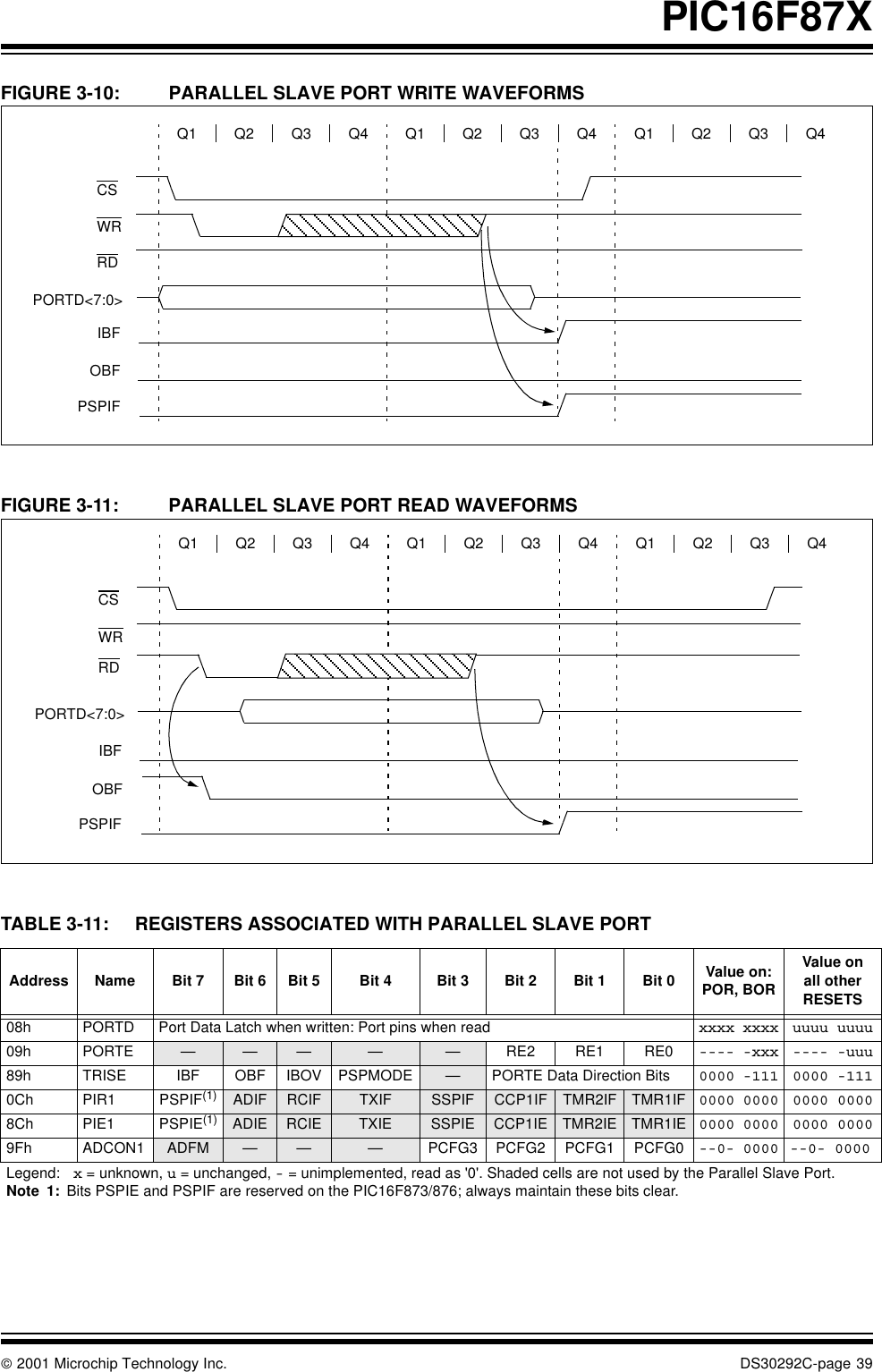
PIC16F87XDS30292C-page 38  2001 Microchip Technology Inc.3.6 Parallel Slave PortThe Parallel Slave Port (PSP) is not implemented onthe PIC16F873 or PIC16F876.PORTD operates as an 8-bit wide Parallel Slave Port ormicroprocessor port, when control bit PSPMODE(TRISE<4>) is set. In Slave mode, it is asynchronouslyreadable and writable by the external world through RDcontrol input pin RE0/RD and WR control input pinRE1/WR.The PSP can directly interface to an 8-bit microproces-sor data bus. The external microprocessor can read orwrite the PORTD latch as an 8-bit latch. Setting bitPSPMODE enables port pin RE0/RD to be the RDinput, RE1/WR to be the WR input and RE2/CS to bethe CS (chip select) input. For this functionality, the cor-responding data direction bits of the TRISE register(TRISE<2:0>) must be configured as inputs (set). TheA/D port configuration bits PCFG3:PCFG0(ADCON1<3:0>) must be set to configure pinsRE2:RE0 as digital I/O. There are actually two 8-bit latches: one for data out-put, and one for data input. The user writes 8-bit datato the PORTD data latch and reads data from the portpin latch (note that they have the same address). In thismode, the TRISD register is ignored, since the externaldevice is controlling the direction of data flow.A write to the PSP occurs when both the CS and WRlines are first detected low. When either the CS or WRlines become high (level triggered), the Input Buffer Full(IBF) status flag bit (TRISE<7>) is set on the Q4 clockcycle, following the next Q2 cycle, to signal the write iscomplete (Figure 3-10). The interrupt flag bit PSPIF(PIR1<7>) is also set on the same Q4 clock cycle. IBFcan only be cleared by reading the PORTD input latch.The Input Buffer Overflow (IBOV) status flag bit(TRISE<5>) is set if a second write to the PSP isattempted when the previous byte has not been readout of the buffer.A read from the PSP occurs when both the CS and RDlines are first detected low. The Output Buffer Full(OBF) status flag bit (TRISE<6>) is cleared immedi-ately (Figure 3-11), indicating that the PORTD latch iswaiting to be read by the external bus. When either theCS or RD pin becomes high (level triggered), the inter-rupt flag bit PSPIF is set on the Q4 clock cycle, follow-ing the next Q2 cycle, indicating that the read iscomplete. OBF remains low until data is written toPORTD by the user firmware.When not in PSP mode, the IBF and OBF bits are heldclear. However, if flag bit IBOV was previously set, itmust be cleared in firmware.An interrupt is generated and latched into flag bitPSPIF when a read or write operation is completed.PSPIF must be cleared by the user in firmware and theinterrupt can be disabled by clearing the interruptenable bit PSPIE (PIE1<7>).FIGURE 3-9: PORTD AND PORTE BLOCK DIAGRAM (PARALLEL SLAVE PORT) Data BusWRPortRDRDxQDCKENQDENPortpinOne bit of PORTDSet Interrupt FlagPSPIF(PIR1<7>)ReadChip SelectWriteRDCSWRTTLTTLTTLTTLNote 1: I/O pins have protection diodes to VDD and VSS.
 2001 Microchip Technology Inc. DS30292C-page 39PIC16F87XFIGURE 3-10: PARALLEL SLAVE PORT WRITE WAVEFORMS  FIGURE 3-11: PARALLEL SLAVE PORT READ WAVEFORMS  TABLE 3-11: REGISTERS ASSOCIATED WITH PARALLEL SLAVE PORTQ1 Q2 Q3 Q4CSQ1 Q2 Q3 Q4 Q1 Q2 Q3 Q4WRRDIBFOBFPSPIFPORTD<7:0>Q1 Q2 Q3 Q4CSQ1 Q2 Q3 Q4 Q1 Q2 Q3 Q4WRIBFPSPIFRDOBFPORTD<7:0>Address Name Bit 7 Bit 6 Bit 5 Bit 4 Bit 3 Bit 2 Bit 1 Bit 0 Value on: POR, BORValue on all other RESETS08h PORTD Port Data Latch when written: Port pins when read xxxx xxxx uuuu uuuu09h PORTE — — — — — RE2 RE1 RE0 ---- -xxx ---- -uuu89h TRISE IBF OBF IBOV PSPMODE —PORTE Data Direction Bits 0000 -111 0000 -1110Ch PIR1 PSPIF(1) ADIF RCIF TXIF SSPIF CCP1IF TMR2IF TMR1IF 0000 0000 0000 00008Ch PIE1 PSPIE(1) ADIE RCIE TXIE SSPIE CCP1IE TMR2IE TMR1IE 0000 0000 0000 00009Fh ADCON1 ADFM — — — PCFG3 PCFG2 PCFG1 PCFG0 --0- 0000 --0- 0000Legend: x = unknown, u = unchanged, - = unimplemented, read as '0'. Shaded cells are not used by the Parallel Slave Port.Note 1: Bits PSPIE and PSPIF are reserved on the PIC16F873/876; always maintain these bits clear.
PIC16F87XDS30292C-page 40  2001 Microchip Technology Inc.NOTES:
 2001 Microchip Technology Inc. DS30292C-page 41PIC16F87X4.0 DATA EEPROM AND FLASH PROGRAM MEMORYThe Data EEPROM and FLASH Program Memory arereadable and writable during normal operation over theentire VDD range. These operations take place on a sin-gle byte for Data EEPROM memory and a single wordfor Program memory. A write operation causes anerase-then-write operation to take place on the speci-fied byte or word. A bulk erase operation may not beissued from user code (which includes removing codeprotection). Access to program memory allows for checksum calcu-lation. The values written to program memory do notneed to be valid instructions. Therefore, up to 14-bitnumbers can be stored in memory for use as calibra-tion parameters, serial numbers, packed 7-bit ASCII,etc. Executing a program memory location containingdata that form an invalid instruction, results in the exe-cution of a NOP instruction. The EEPROM Data memory is rated for high erase/write cycles (specification D120). The FLASH programmemory is rated much lower (specification D130),because EEPROM data memory can be used to storefrequently updated values. An on-chip timer controlsthe write time and it will vary with voltage and tempera-ture, as well as from chip to chip. Please refer to thespecifications for exact limits (specifications D122 andD133).A byte or word write automatically erases the locationand writes the new value (erase before write). Writingto EEPROM data memory does not impact the opera-tion of the device. Writing to program memory willcease the execution of instructions until the write iscomplete. The program memory cannot be accessedduring the write. During the write operation, the oscilla-tor continues to run, the peripherals continue to func-tion and interrupt events will be detected andessentially “queued” until the write is complete. Whenthe write completes, the next instruction in the pipelineis executed and the branch to the interrupt vector willtake place, if the interrupt is enabled and occurred dur-ing the write.Read and write access to both memories take placeindirectly through a set of Special Function Registers(SFR). The six SFRs used are:•EEDATA•EEDATH•EEADR•EEADRH•EECON1•EECON2The EEPROM data memory allows byte read and writeoperations without interfering with the normal operationof the microcontroller. When interfacing to EEPROMdata memory, the EEADR register holds the address tobe accessed. Depending on the operation, the EEDATAregister holds the data to be written, or the data read, atthe address in EEADR. The PIC16F873/874 deviceshave 128 bytes of EEPROM data memory and there-fore, require that the MSb of EEADR remain clear. TheEEPROM data memory on these devices do not wraparound to 0, i.e., 0x80 in the EEADR does not map to0x00. The PIC16F876/877 devices have 256 bytes ofEEPROM data memory and therefore, uses all 8-bits ofthe EEADR.The FLASH program memory allows non-intrusiveread access, but write operations cause the device tostop executing instructions, until the write completes.When interfacing to the program memory, theEEADRH:EEADR registers form a two-byte word,which holds the 13-bit address of the memory locationbeing accessed. The register combination ofEEDATH:EEDATA holds the 14-bit data for writes, orreflects the value of program memory after a read oper-ation. Just as in EEPROM data memory accesses, thevalue of the EEADRH:EEADR registers must be withinthe valid range of program memory, depending on thedevice: 0000h to 1FFFh for the PIC16F873/874, or0000h to 3FFFh for the PIC16F876/877. Addressesoutside of this range do not wrap around to 0000h (i.e.,4000h does not map to 0000h on the PIC16F877).4.1 EECON1 and EECON2 RegistersThe EECON1 register is the control register for config-uring and initiating the access. The EECON2 register isnot a physically implemented register, but is usedexclusively in the memory write sequence to preventinadvertent writes.There are many bits used to control the read and writeoperations to EEPROM data and FLASH programmemory. The EEPGD bit determines if the access willbe a program or data memory access. When clear, anysubsequent operations will work on the EEPROM datamemory. When set, all subsequent operations willoperate in the program memory.Read operations only use one additional bit, RD, whichinitiates the read operation from the desired memorylocation. Once this bit is set, the value of the desiredmemory location will be available in the data registers.This bit cannot be cleared by firmware. It is automati-cally cleared at the end of the read operation. ForEEPROM data memory reads, the data will be avail-able in the EEDATA register in the very next instructioncycle after the RD bit is set. For program memoryreads, the data will be loaded into theEEDATH:EEDATA registers, following the secondinstruction after the RD bit is set.
PIC16F87XDS30292C-page 42  2001 Microchip Technology Inc.Write operations have two control bits, WR and WREN,and two status bits, WRERR and EEIF. The WREN bitis used to enable or disable the write operation. WhenWREN is clear, the write operation will be disabled.Therefore, the WREN bit must be set before executinga write operation. The WR bit is used to initiate the writeoperation. It also is automatically cleared at the end ofthe write operation. The interrupt flag EEIF is used todetermine when the memory write completes. This flagmust be cleared in software before setting the WR bit.For EEPROM data memory, once the WREN bit andthe WR bit have been set, the desired memory addressin EEADR will be erased, followed by a write of the datain EEDATA. This operation takes place in parallel withthe microcontroller continuing to execute normally.When the write is complete, the EEIF flag bit will be set.For program memory, once the WREN bit and the WRbit have been set, the microcontroller will cease to exe-cute instructions. The desired memory location pointedto by EEADRH:EEADR will be erased. Then, the datavalue in EEDATH:EEDATA will be programmed. Whencomplete, the EEIF flag bit will be set and the microcon-troller will continue to execute code.The WRERR bit is used to indicate when thePIC16F87X device has been reset during a write oper-ation. WRERR should be cleared after Power-onReset. Thereafter, it should be checked on any otherRESET. The WRERR bit is set when a write operationis interrupted by a MCLR Reset, or a WDT Time-outReset, during normal operation. In these situations, fol-lowing a RESET, the user should check the WRERR bitand rewrite the memory location, if set. The contents ofthe data registers, address registers and EEPGD bitare not affected by either MCLR Reset, or WDT Time-out Reset, during normal operation.REGISTER 4-1: EECON1 REGISTER (ADDRESS 18Ch)                      R/W-x U-0 U-0 U-0 R/W-x R/W-0 R/S-0 R/S-0EEPGD ———WRERR WREN WR RDbit 7 bit 0bit 7 EEPGD: Program/Data EEPROM Select bit1 = Accesses program memory0 = Accesses data memory(This bit cannot be changed while a read or write operation is in progress)bit 6-4 Unimplemented: Read as '0'bit 3 WRERR: EEPROM Error Flag bit1 = A write operation is prematurely terminated(any MCLR Reset or any WDT Reset during normal operation)0 = The write operation completedbit 2 WREN: EEPROM Write Enable bit1 = Allows write cycles0 = Inhibits write to the EEPROMbit 1 WR: Write Control bit1 = Initiates a write cycle. (The bit is cleared by hardware once write is complete. The WR bit can only be set (not cleared) in software.)0 = Write cycle to the EEPROM is completebit 0 RD: Read Control bit1 = Initiates an EEPROM read. (RD is cleared in hardware. The RD bit can only be set (not cleared) in software.)0 = Does not initiate an EEPROM readLegend:R = Readable bit W = Writable bit U = Unimplemented bit, read as ‘0’- n = Value at POR ’1’ = Bit is set ’0’ = Bit is cleared x = Bit is unknown
 2001 Microchip Technology Inc. DS30292C-page 43PIC16F87X4.2 Reading the EEPROM Data MemoryReading EEPROM data memory only requires that thedesired address to access be written to the EEADRregister and clear the EEPGD bit. After the RD bit is set,data will be available in the EEDATA register on thevery next instruction cycle. EEDATA will hold this valueuntil another read operation is initiated or until it is writ-ten by firmware. The steps to reading the EEPROM data memory are:1. Write the address to EEDATA. Make sure thatthe address is not larger than the memory sizeof the PIC16F87X device.2. Clear the EEPGD bit to point to EEPROM datamemory.3. Set the RD bit to start the read operation.4. Read the data from the EEDATA register.EXAMPLE 4-1:  EEPROM DATA READ4.3 Writing to the EEPROM Data MemoryThere are many steps in writing to the EEPROM datamemory. Both address and data values must be writtento the SFRs. The EEPGD bit must be cleared, and theWREN bit must be set, to enable writes. The WREN bitshould be kept clear at all times, except when writing tothe EEPROM data. The WR bit can only be set if theWREN bit was set in a previous operation, i.e., theyboth cannot be set in the same operation. The WRENbit should then be cleared by firmware after the write.Clearing the WREN bit before the write actually com-pletes will not terminate the write in progress. Writes to EEPROM data memory must also be pref-aced with a special sequence of instructions, that pre-vent inadvertent write operations. This is a sequence offive instructions that must be executed without interrup-tions. The firmware should verify that a write is not inprogress, before starting another cycle.The steps to write to EEPROM data memory are:1. If step 10 is not implemented, check the WR bitto see if a write is in progress.2. Write the address to EEADR. Make sure that theaddress is not larger than the memory size ofthe PIC16F87X device.3. Write the 8-bit data value to be programmed inthe EEDATA register.4. Clear the EEPGD bit to point to EEPROM datamemory.5. Set the WREN bit to enable program operations.6. Disable interrupts (if enabled).7. Execute the special five instruction sequence:•Write 55h to EECON2 in two steps (first to W, then to EECON2)•Write AAh to EECON2 in two steps (first to W, then to EECON2)•Set the WR bit8. Enable interrupts (if using interrupts).9. Clear the WREN bit to disable program opera-tions.10. At the completion of the write cycle, the WR bitis cleared and the EEIF interrupt flag bit is set.(EEIF must be cleared by firmware.) If step 1 isnot implemented, then firmware should checkfor EEIF to be set, or WR to clear, to indicate theend of the program cycle.EXAMPLE 4-2: EEPROM DATA WRITEBSF    STATUS, RP1    ;BCF    STATUS, RP0    ;Bank 2MOVF   ADDR, W        ;Write addressMOVWF  EEADR          ;to read fromBSF    STATUS, RP0    ;Bank 3BCF    EECON1, EEPGD  ;Point to Data memoryBSF    EECON1, RD     ;Start read operationBCF    STATUS, RP0    ;Bank 2MOVF   EEDATA, W      ;W = EEDATABSF    STATUS, RP1   ;BSF    STATUS, RP0   ;Bank 3BTFSC  EECON1, WR    ;Wait forGOTO   $-1           ;write to finishBCF    STATUS, RP0   ;Bank 2MOVF   ADDR, W       ;Address toMOVWF  EEADR         ;write toMOVF   VALUE, W      ;Data toMOVWF  EEDATA        ;writeBSF    STATUS, RP0   ;Bank 3BCF    EECON1, EEPGD ;Point to Data memoryBSF    EECON1, WREN  ;Enable writes                      ;Only disable interruptsBCF    INTCON, GIE   ;if already enabled,                     ;otherwise discardMOVLW  0x55          ;Write 55h toMOVWF  EECON2        ;EECON2MOVLW  0xAA          ;Write AAh toMOVWF  EECON2        ;EECON2BSF    EECON1, WR    ;Start write operation                     ;Only enable interruptsBSF    INTCON, GIE   ;if using interrupts,                     ;otherwise discardBCF    EECON1, WREN  ;Disable writes
PIC16F87XDS30292C-page 44  2001 Microchip Technology Inc.4.4 Reading the FLASH Program MemoryReading FLASH program memory is much like that ofEEPROM data memory, only two NOP instructions mustbe inserted after the RD bit is set. These two instructioncycles that the NOP instructions execute, will be usedby the microcontroller to read the data out of programmemory and insert the value into theEEDATH:EEDATA registers. Data will be available fol-lowing the second NOP instruction. EEDATH andEEDATA will hold their value until another read opera-tion is initiated, or until they are written by firmware. The steps to reading the FLASH program memory are:1. Write the address to EEADRH:EEADR. Makesure that the address is not larger than the mem-ory size of the PIC16F87X device.2. Set the EEPGD bit to point to FLASH programmemory.3. Set the RD bit to start the read operation.4. Execute two NOP instructions to allow the micro-controller to read out of program memory.5. Read the data from the EEDATH:EEDATA registers.EXAMPLE 4-3: FLASH PROGRAM READ4.5 Writing to the FLASH Program MemoryWriting to FLASH program memory is unique, in thatthe microcontroller does not execute instructions whileprogramming is taking place. The oscillator continuesto run and all peripherals continue to operate andqueue interrupts, if enabled. Once the write operationcompletes (specification D133), the processor beginsexecuting code from where it left off. The other impor-tant difference when writing to FLASH program mem-ory, is that the WRT configuration bit, when clear,prevents any writes to program memory (see Table 4-1).Just like EEPROM data memory, there are many stepsin writing to the FLASH program memory. Both addressand data values must be written to the SFRs. TheEEPGD bit must be set, and the WREN bit must be setto enable writes. The WREN bit should be kept clear atall times, except when writing to the FLASH Programmemory. The WR bit can only be set if the WREN bitwas set in a previous operation, i.e., they both cannotbe set in the same operation. The WREN bit shouldthen be cleared by firmware after the write. Clearing theWREN bit before the write actually completes will notterminate the write in progress. Writes to program memory must also be prefaced witha special sequence of instructions that prevent inad-vertent write operations. This is a sequence of fiveinstructions that must be executed without interruptionfor each byte written. These instructions must then befollowed by two NOP instructions to allow the microcon-troller to setup for the write operation. Once the write iscomplete, the execution of instructions starts with theinstruction after the second NOP.The steps to write to program memory are:1. Write the address to EEADRH:EEADR. Makesure that the address is not larger than the mem-ory size of the PIC16F87X device.2. Write the 14-bit data value to be programmed inthe EEDATH:EEDATA registers.3. Set the EEPGD bit to point to FLASH programmemory.4. Set the WREN bit to enable program operations.5. Disable interrupts (if enabled).6. Execute the special five instruction sequence:•Write 55h to EECON2 in two steps (first to W, then to EECON2)•Write AAh to EECON2 in two steps (first to W, then to EECON2)•Set the WR bit7. Execute two NOP instructions to allow the micro-controller to setup for write operation.8. Enable interrupts (if using interrupts).9. Clear the WREN bit to disable program operations.BSF    STATUS, RP1   ;BCF    STATUS, RP0   ;Bank 2MOVF   ADDRL, W      ;Write theMOVWF  EEADR         ;address bytesMOVF   ADDRH,W       ;for the desiredMOVWF  EEADRH        ;address to readBSF    STATUS, RP0   ;Bank 3BSF    EECON1, EEPGD ;Point to Program memoryBSF    EECON1, RD    ;Start read operationNOP                  ;Required two NOPsNOP                  ;BCF    STATUS, RP0   ;Bank 2MOVF   EEDATA, W     ;DATAL = EEDATAMOVWF  DATAL         ;MOVF   EEDATH,W      ;DATAH = EEDATHMOVWF  DATAH         ;
 2001 Microchip Technology Inc. DS30292C-page 45PIC16F87XAt the completion of the write cycle, the WR bit iscleared and the EEIF interrupt flag bit is set. (EEIFmust be cleared by firmware.) Since the microcontrollerdoes not execute instructions during the write cycle, thefirmware does not necessarily have to check eitherEEIF, or WR, to determine if the write had finished.EXAMPLE 4-4: FLASH PROGRAM WRITE4.6 Write VerifyThe PIC16F87X devices do not automatically verify thevalue written during a write operation. Depending onthe application, good programming practice may dic-tate that the value written to memory be verified againstthe original value. This should be used in applicationswhere excessive writes can stress bits near the speci-fied endurance limits.4.7 Protection Against Spurious WritesThere are conditions when the device may not want towrite to the EEPROM data memory or FLASH programmemory. To protect against these spurious write condi-tions, various mechanisms have been built into thePIC16F87X devices. On power-up, the WREN bit iscleared and the Power-up Timer (if enabled) preventswrites.The write initiate sequence, and the WREN bittogether, help prevent any accidental writes duringbrown-out, power glitches, or firmware malfunction.4.8 Operation While Code ProtectedThe PIC16F87X devices have two code protect mecha-nisms, one bit for EEPROM data memory and two bits forFLASH program memory. Data can be read and writtento the EEPROM data memory, regardless of the state ofthe code protection bit, CPD. When code protection isenabled and CPD cleared, external access via ICSP isdisabled, regardless of the state of the program memorycode protect bits. This prevents the contents of EEPROMdata memory from being read out of the device.The state of the program memory code protect bits,CP0 and CP1, do not affect the execution of instruc-tions out of program memory. The PIC16F87X devicescan always read the values in program memory,regardless of the state of the code protect bits. How-ever, the state of the code protect bits and the WRT bitwill have different effects on writing to program mem-ory. Table 4-1 shows the effect of the code protect bitsand the WRT bit on program memory. Once code protection has been enabled for eitherEEPROM data memory or FLASH program memory,only a full erase of the entire device will disable codeprotection.BSF    STATUS, RP1   ;BCF    STATUS, RP0   ;Bank 2MOVF   ADDRL, W      ;Write addressMOVWF  EEADR         ;of desiredMOVF   ADDRH, W      ;program memoryMOVWF  EEADRH        ;locationMOVF   VALUEL, W     ;Write value toMOVWF  EEDATA        ;program atMOVF   VALUEH, W     ;desired memoryMOVWF  EEDATH        ;locationBSF    STATUS, RP0   ;Bank 3BSF    EECON1, EEPGD ;Point to Program memoryBSF    EECON1, WREN  ;Enable writes                     ;Only disable interruptsBCF    INTCON, GIE   ;if already enabled,                     ;otherwise discardMOVLW  0x55          ;Write 55h toMOVWF  EECON2        ;EECON2MOVLW  0xAA          ;Write AAh toMOVWF  EECON2        ;EECON2BSF    EECON1, WR    ;Start write operationNOP                  ;Two NOPs to allow microNOP                  ;to setup for write                     ;Only enable interruptsBSF    INTCON, GIE   ;if using interrupts,                     ;otherwise discardBCF    EECON1, WREN  ;Disable writes
PIC16F87XDS30292C-page 46  2001 Microchip Technology Inc.4.9 FLASH Program Memory Write ProtectionThe configuration word contains a bit that write protectsthe FLASH program memory, called WRT. This bit canonly be accessed when programming the PIC16F87Xdevice via ICSP. Once write protection is enabled, onlyan erase of the entire device will disable it. Whenenabled, write protection prevents any writes to FLASHprogram memory. Write protection does not affect pro-gram memory reads.TABLE 4-1: READ/WRITE STATE OF INTERNAL FLASH PROGRAM MEMORYTABLE 4-2: REGISTERS ASSOCIATED WITH DATA EEPROM/PROGRAM FLASH Configuration Bits Memory Location Internal Read Internal Write ICSP Read ICSP WriteCP1 CP0 WRT00x All program memory Yes No  No No010 Unprotected areas Yes No Yes No010 Protected areas Yes No No No011 Unprotected areas Yes Yes Yes No011 Protected areas Yes No No No100 Unprotected areas Yes No Yes No100 Protected areas Yes No No No101 Unprotected areas Yes Yes Yes No101 Protected areas Yes No No No110 All program memory Yes No Yes Yes111 All program memory Yes Yes Yes YesAddress Name Bit 7 Bit 6 Bit 5 Bit 4 Bit 3 Bit 2 Bit 1 Bit 0 Value on:POR,BORValue on all other RESETS0Bh, 8Bh,10Bh, 18BhINTCON GIE PEIE T0IE INTE RBIE T0IF INTF RBIF 0000 000x 0000 000u10Dh EEADR EEPROM Address Register, Low Byte xxxx xxxx uuuu uuuu10Fh EEADRH — — — EEPROM Address, High Byte xxxx xxxx uuuu uuuu10Ch EEDATA EEPROM Data Register, Low Byte xxxx xxxx uuuu uuuu10Eh EEDATH — — EEPROM Data Register, High Byte xxxx xxxx uuuu uuuu18Ch EECON1 EEPGD — — — WRERR WREN WR RD x--- x000 x--- u00018Dh EECON2 EEPROM Control Register2 (not a physical register) ——8Dh PIE2 —(1) —EEIE BCLIE — — CCP2IE -r-0 0--0 -r-0 0--00Dh PIR2 —(1) —EEIF BCLIF — — CCP2IF -r-0 0--0 -r-0 0--0Legend:  x = unknown, u = unchanged, r = reserved, - = unimplemented, read as '0'. Shaded cells are not used during FLASH/EEPROM access.Note 1: These bits are reserved; always maintain these bits clear.
 2001 Microchip Technology Inc. DS30292C-page 47PIC16F87X5.0 TIMER0 MODULEThe Timer0 module timer/counter has the following fea-tures:•8-bit timer/counter•Readable and writable•8-bit software programmable prescaler•Internal or external clock select•Interrupt on overflow from FFh to 00h•Edge select for external clockFigure 5-1 is a block diagram of the Timer0 module andthe prescaler shared with the WDT.Additional information on the Timer0 module is avail-able in the PICmicro™ Mid-Range MCU Family Refer-ence Manual (DS33023). Timer mode is selected by clearing bit T0CS(OPTION_REG<5>). In Timer mode, the Timer0 mod-ule will increment every instruction cycle (without pres-caler). If the TMR0 register is written, the increment isinhibited for the following two instruction cycles. Theuser can work around this by writing an adjusted valueto the TMR0 register.Counter mode is selected by setting bit T0CS(OPTION_REG<5>). In Counter mode, Timer0 willincrement either on every rising, or falling edge of pinRA4/T0CKI. The incrementing edge is determined bythe Timer0 Source Edge Select bit, T0SE(OPTION_REG<4>). Clearing bit T0SE selects the ris-ing edge. Restrictions on the external clock input arediscussed in detail in Section 5.2.The prescaler is mutually exclusively shared betweenthe Timer0 module and the Watchdog Timer. The pres-caler is not readable or writable. Section 5.3 details theoperation of the prescaler.5.1 Timer0 InterruptThe TMR0 interrupt is generated when the TMR0 reg-ister overflows from FFh to 00h. This overflow sets bitT0IF (INTCON<2>). The interrupt can be masked byclearing bit T0IE (INTCON<5>). Bit T0IF must becleared in software by the Timer0 module Interrupt Ser-vice Routine before re-enabling this interrupt. TheTMR0 interrupt cannot awaken the processor fromSLEEP, since the timer is shut-off during SLEEP.FIGURE 5-1: BLOCK DIAGRAM OF THE TIMER0/WDT PRESCALER     RA4/T0CKIT0SEpinMUXCLKOUT (= FOSC/4)SYNC2Cycles TMR0 Reg8-bit Prescaler8 - to - 1MUXMUXM U XWatchdogTimerPSA0101WDTTime-outPS2:PS08Note: T0CS, T0SE, PSA, PS2:PS0 are (OPTION_REG<5:0>).PSAWDT Enable bitMUX0101Data BusSet Flag Bit T0IFon Overflow8PSAT0CSPRESCALER
PIC16F87XDS30292C-page 48  2001 Microchip Technology Inc.5.2 Using Timer0 with an External ClockWhen no prescaler is used, the external clock input isthe same as the prescaler output. The synchronizationof T0CKI with the internal phase clocks is accom-plished by sampling the prescaler output on the Q2 andQ4 cycles of the internal phase clocks. Therefore, it isnecessary for T0CKI to be high for at least 2Tosc (anda small RC delay of 20 ns) and low for at least 2Tosc(and a small RC delay of 20 ns). Refer to the electricalspecification of the desired device.5.3 PrescalerThere is only one prescaler available, which is mutuallyexclusively shared between the Timer0 module and theWatchdog Timer. A prescaler assignment for theTimer0 module means that there is no prescaler for theWatchdog Timer, and vice-versa. This prescaler is notreadable or writable (see Figure 5-1). The PSA and PS2:PS0 bits (OPTION_REG<3:0>)determine the prescaler assignment and prescale ratio.When assigned to the Timer0 module, all instructionswriting to the TMR0 register (e.g. CLRF 1, MOVWF 1,BSF 1,x....etc.) will clear the prescaler. When assignedto WDT, a CLRWDT instruction will clear the prescaleralong with the Watchdog Timer. The prescaler is notreadable or writable. REGISTER 5-1: OPTION_REG REGISTER                                     Note: Writing to TMR0, when the prescaler isassigned to Timer0, will clear the prescalercount, but will not change the prescalerassignment.R/W-1 R/W-1 R/W-1 R/W-1 R/W-1 R/W-1 R/W-1 R/W-1RBPU INTEDG T0CS T0SE PSA PS2 PS1 PS0bit 7 bit 0bit 7 RBPUbit 6 INTEDGbit 5 T0CS: TMR0 Clock Source Select bit 1 = Transition on T0CKI pin 0 = Internal instruction cycle clock (CLKOUT) bit 4 T0SE: TMR0 Source Edge Select bit 1 = Increment on high-to-low transition on T0CKI pin 0 = Increment on low-to-high transition on T0CKI pin bit 3 PSA: Prescaler Assignment bit 1 = Prescaler is assigned to the WDT 0 = Prescaler is assigned to the Timer0 module bit 2-0 PS2:PS0: Prescaler Rate Select bits    Legend:R = Readable bit W = Writable bit U = Unimplemented bit, read as ‘0’- n = Value at POR ’1’ = Bit is set ’0’ = Bit is cleared x = Bit is unknown0000010100111001011101111 : 21 : 41 : 81 : 161 : 321 : 641 : 1281 : 2561 : 11 : 21 : 41 : 81 : 161 : 321 : 641 : 128Bit Value TMR0 Rate WDT RateNote: To avoid an unintended device RESET, the instruction sequence shown in the PICmicro™ Mid-Range MCUFamily Reference Manual (DS33023) must be executed when changing the prescaler assignment fromTimer0 to the WDT. This sequence must be followed even if the WDT is disabled.
 2001 Microchip Technology Inc. DS30292C-page 49PIC16F87XTABLE 5-1: REGISTERS ASSOCIATED WITH TIMER0    Address Name Bit 7 Bit 6 Bit 5 Bit 4 Bit 3 Bit 2 Bit 1 Bit 0 Value on: POR,BORValue on all other RESETS01h,101h TMR0 Timer0 Module’s Register xxxx xxxx uuuu uuuu0Bh,8Bh,10Bh,18Bh INTCON GIE PEIE T0IE INTE RBIE T0IF INTF RBIF 0000 000x 0000 000u81h,181h OPTION_REG RBPU INTEDG T0CS T0SE PSA PS2 PS1 PS0 1111 1111 1111 1111Legend: x = unknown, u = unchanged, - = unimplemented locations read as '0'. Shaded cells are not used by Timer0.
PIC16F87XDS30292C-page 50  2001 Microchip Technology Inc.NOTES:
 2001 Microchip Technology Inc. DS30292C-page 51PIC16F87X6.0 TIMER1 MODULEThe Timer1 module is a 16-bit timer/counter consistingof two 8-bit registers (TMR1H and TMR1L), which arereadable and writable. The TMR1 Register pair(TMR1H:TMR1L) increments from 0000h to FFFFhand rolls over to 0000h. The TMR1 Interrupt, if enabled,is generated on overflow, which is latched in interruptflag bit TMR1IF (PIR1<0>). This interrupt can beenabled/disabled by setting/clearing TMR1 interruptenable bit TMR1IE (PIE1<0>).Timer1 can operate in one of two modes:•As a timer•As a counterThe operating mode is determined by the clock selectbit, TMR1CS (T1CON<1>).In Timer mode, Timer1 increments every instructioncycle.   In Counter mode, it increments on every risingedge of the external clock input.Timer1 can be enabled/disabled by setting/clearingcontrol bit TMR1ON (T1CON<0>). Timer1 also has an internal “RESET input”. ThisRESET can be generated by either of the two CCPmodules (Section 8.0). Register 6-1 shows the Timer1control register.When the Timer1 oscillator is enabled (T1OSCEN isset), the RC1/T1OSI/CCP2 and RC0/T1OSO/T1CKIpins become inputs. That is, the TRISC<1:0> value isignored, and these pins read as ‘0’.Additional information on timer modules is available inthe PICmicro™ Mid-Range MCU Family ReferenceManual (DS33023).REGISTER 6-1: T1CON: TIMER1 CONTROL REGISTER (ADDRESS 10h)                   U-0 U-0 R/W-0 R/W-0 R/W-0 R/W-0 R/W-0 R/W-0— — T1CKPS1 T1CKPS0 T1OSCEN T1SYNC TMR1CS TMR1ONbit 7 bit 0bit 7-6 Unimplemented: Read as '0'bit 5-4 T1CKPS1:T1CKPS0: Timer1 Input Clock Prescale Select bits11 = 1:8 Prescale value10 = 1:4 Prescale value01 = 1:2 Prescale value00 = 1:1 Prescale valuebit 3 T1OSCEN: Timer1 Oscillator Enable Control bit1 = Oscillator is enabled0 = Oscillator is shut-off (the oscillator inverter is turned off to eliminate power drain)bit 2 T1SYNC: Timer1 External Clock Input Synchronization Control bitWhen TMR1CS = 1:1 = Do not synchronize external clock input0 = Synchronize external clock inputWhen TMR1CS = 0:This bit is ignored. Timer1 uses the internal clock when TMR1CS = 0.bit 1 TMR1CS: Timer1 Clock Source Select bit1 = External clock from pin RC0/T1OSO/T1CKI (on the rising edge)0 = Internal clock (FOSC/4)    bit 0 TMR1ON: Timer1 On bit1 = Enables Timer10 = Stops Timer1Legend:R = Readable bit W = Writable bit U = Unimplemented bit, read as ‘0’- n = Value at POR ’1’ = Bit is set ’0’ = Bit is cleared x = Bit is unknown
PIC16F87XDS30292C-page 52  2001 Microchip Technology Inc.6.1 Timer1 Operation in Timer ModeTimer mode is selected by clearing the TMR1CS(T1CON<1>) bit. In this mode, the input clock to thetimer is FOSC/4. The synchronize control bit T1SYNC(T1CON<2>) has no effect, since the internal clock isalways in sync.6.2 Timer1 Counter OperationTimer1 may operate in either a Synchronous, or anAsynchronous mode, depending on the setting of theTMR1CS bit.When Timer1 is being incremented via an externalsource, increments occur on a rising edge. After Timer1is enabled in Counter mode, the module must first havea falling edge before the counter begins to increment.FIGURE 6-1: TIMER1 INCREMENTING EDGE  6.3 Timer1 Operation in Synchronized Counter ModeCounter mode is selected by setting bit TMR1CS. Inthis mode, the timer increments on every rising edge ofclock input on pin RC1/T1OSI/CCP2, when bitT1OSCEN is set, or on pin RC0/T1OSO/T1CKI, whenbit T1OSCEN is cleared.If T1SYNC is cleared, then the external clock input issynchronized with internal phase clocks. The synchro-nization is done after the prescaler stage. Theprescaler stage is an asynchronous ripple-counter.In this configuration, during SLEEP mode, Timer1 willnot increment even if the external clock is present,since the synchronization circuit is shut-off. Theprescaler, however, will continue to increment.FIGURE 6-2: TIMER1 BLOCK DIAGRAMT1CKI(Default High)T1CKI(Default Low)Note: Arrows indicate counter increments.TMR1H TMR1LT1OSC T1SYNCTMR1CST1CKPS1:T1CKPS0 Q ClockT1OSCENEnableOscillator(1)FOSC/4InternalClockTMR1ONOn/OffPrescaler1, 2, 4, 8Synchronizedet1001SynchronizedClock Input2RC0/T1OSO/T1CKIRC1/T1OSI/CCP2(2)Note 1: When the T1OSCEN bit is cleared, the inverter is turned off. This eliminates power drain.Set Flag bitTMR1IF onOverflow TMR1
 2001 Microchip Technology Inc. DS30292C-page 53PIC16F87X6.4 Timer1 Operation in Asynchronous Counter ModeIf control bit T1SYNC (T1CON<2>) is set, the externalclock input is not synchronized. The timer continues toincrement asynchronous to the internal phase clocks.The timer will continue to run during SLEEP and cangenerate an interrupt-on-overflow, which will wake-upthe processor. However, special precautions in soft-ware are needed to read/write the timer (Section 6.4.1).In Asynchronous Counter mode, Timer1 cannot beused as a time-base for capture or compare opera-tions.6.4.1 READING AND WRITING TIMER1 IN ASYNCHRONOUS COUNTER MODEReading TMR1H or TMR1L while the timer is runningfrom an external asynchronous clock, will guarantee avalid read (taken care of in hardware). However, theuser should keep in mind that reading the 16-bit timerin two 8-bit values itself, poses certain problems, sincethe timer may overflow between the reads. For writes, it is recommended that the user simply stopthe timer and write the desired values. A write conten-tion may occur by writing to the timer registers, whilethe register is incrementing. This may produce anunpredictable value in the timer register.Reading the 16-bit value requires some care. Exam-ples 12-2 and 12-3 in the PICmicro™ Mid-Range MCUFamily Reference Manual (DS33023) show how toread and write Timer1 when it is running in Asynchro-nous mode.6.5 Timer1 OscillatorA crystal oscillator circuit is built-in between pins T1OSI(input) and T1OSO (amplifier output). It is enabled bysetting control bit T1OSCEN (T1CON<3>). The oscilla-tor is a low power oscillator, rated up to 200 kHz. It willcontinue to run during SLEEP. It is primarily intendedfor use with a 32 kHz crystal. Table 6-1 shows thecapacitor selection for the Timer1 oscillator. The Timer1 oscillator is identical to the LP oscillator.The user must provide a software time delay to ensureproper oscillator start-up.TABLE 6-1: CAPACITOR SELECTION FOR THE TIMER1 OSCILLATOR 6.6 Resetting Timer1 using a CCP Trigger OutputIf the CCP1 or CCP2 module is configured in Comparemode to generate a “special event trigger”(CCP1M3:CCP1M0 = 1011), this signal will resetTimer1.Timer1 must be configured for either Timer or Synchro-nized Counter mode to take advantage of this feature.If Timer1 is running in Asynchronous Counter mode,this RESET operation may not work.In the event that a write to Timer1 coincides with a spe-cial event trigger from CCP1 or CCP2, the write willtake precedence.In this mode of operation, the CCPRxH:CCPRxL regis-ter pair effectively becomes the period register forTimer1. Osc Type Freq. C1 C2LP 32 kHz 33 pF 33 pF100 kHz 15 pF 15 pF200 kHz 15 pF 15 pFThese values are for design guidance only.Crystals Tested:32.768 kHz Epson C-001R32.768K-A ± 20 PPM100 kHz Epson C-2 100.00 KC-P ± 20 PPM200 kHz STD XTL 200.000 kHz ± 20 PPMNote 1: Higher capacitance increases the stability of oscillator, but also increases the start-up time. 2: Since each resonator/crystal has its own characteristics, the user should consult the resonator/crystal manufacturer for appro-priate values of external components. Note: The special event triggers from the CCP1and CCP2 modules will not set interruptflag bit TMR1IF (PIR1<0>).
PIC16F87XDS30292C-page 54  2001 Microchip Technology Inc.6.7 Resetting of Timer1 Register Pair (TMR1H, TMR1L)TMR1H and TMR1L registers are not reset to 00h on aPOR, or any other RESET, except by the CCP1 andCCP2 special event triggers.T1CON register is reset to 00h on a Power-on Reset,or a Brown-out Reset, which shuts off the timer andleaves a 1:1 prescale. In all other RESETS, the registeris unaffected.6.8 Timer1 PrescalerThe prescaler counter is cleared on writes to theTMR1H or TMR1L registers.TABLE 6-2: REGISTERS ASSOCIATED WITH TIMER1 AS A TIMER/COUNTER     Address Name Bit 7 Bit 6 Bit 5 Bit 4 Bit 3 Bit 2 Bit 1 Bit 0 Value on:POR,BORValue on all other RESETS0Bh,8Bh,10Bh, 18Bh INTCON GIE PEIE T0IE INTE RBIE T0IF INTF RBIF 0000 000x 0000 000u0Ch PIR1 PSPIF(1) ADIF RCIF TXIF SSPIF CCP1IF TMR2IF TMR1IF 0000 0000 0000 00008Ch PIE1 PSPIE(1) ADIE RCIE TXIE SSPIE CCP1IE TMR2IE TMR1IE 0000 0000 0000 00000Eh TMR1L Holding Register for the Least Significant Byte of the 16-bit TMR1 Register xxxx xxxx uuuu uuuu0Fh TMR1H Holding Register for the Most Significant Byte of the 16-bit TMR1 Register xxxx xxxx uuuu uuuu10h T1CON — — T1CKPS1 T1CKPS0 T1OSCEN T1SYNC TMR1CS TMR1ON --00 0000 --uu uuuuLegend:  x = unknown, u = unchanged, - = unimplemented, read as '0'. Shaded cells are not used by the Timer1 module.Note 1: Bits PSPIE and PSPIF are reserved on the PIC16F873/876; always maintain these bits clear.
 2001 Microchip Technology Inc. DS30292C-page 55PIC16F87X7.0 TIMER2 MODULETimer2 is an 8-bit timer with a prescaler and apostscaler. It can be used as the PWM time-base forthe PWM mode of the CCP module(s). The TMR2 reg-ister is readable and writable, and is cleared on anydevice RESET.The input clock (FOSC/4) has a prescale option of 1:1,1:4, or 1:16, selected by control bitsT2CKPS1:T2CKPS0 (T2CON<1:0>).The Timer2 module has an 8-bit period register, PR2.Timer2 increments from 00h until it matches PR2 andthen resets to 00h on the next increment cycle. PR2 isa readable and writable register. The PR2 register isinitialized to FFh upon RESET.The match output of TMR2 goes through a 4-bitpostscaler (which gives a 1:1 to 1:16 scaling inclusive)to generate a TMR2 interrupt (latched in flag bitTMR2IF, (PIR1<1>)).Timer2 can be shut-off by clearing control bit TMR2ON(T2CON<2>), to minimize power consumption.Register 7-1 shows the Timer2 control register.Additional information on timer modules is available inthe PICmicro™ Mid-Range MCU Family ReferenceManual (DS33023).FIGURE 7-1: TIMER2 BLOCK DIAGRAMREGISTER 7-1: T2CON: TIMER2 CONTROL REGISTER (ADDRESS 12h)                   ComparatorTMR2Sets FlagTMR2 RegOutput(1)RESETPostscalerPrescalerPR2 Reg2FOSC/41:1 1:161:1, 1:4, 1:16EQ4bit TMR2IFNote 1:TMR2 register output can be software selected by theSSP module as a baud clock.toT2OUTPS3:T2OUTPS0T2CKPS1:T2CKPS0U-0 R/W-0 R/W-0 R/W-0 R/W-0 R/W-0 R/W-0 R/W-0—TOUTPS3 TOUTPS2 TOUTPS1 TOUTPS0 TMR2ON T2CKPS1 T2CKPS0bit 7 bit 0bit 7 Unimplemented: Read as '0'bit 6-3 TOUTPS3:TOUTPS0: Timer2 Output Postscale Select bits0000 = 1:1 Postscale0001 = 1:2 Postscale0010 = 1:3 Postscale•••1111 = 1:16 Postscalebit 2 TMR2ON: Timer2 On bit1 = Timer2 is on0 = Timer2 is offbit 1-0 T2CKPS1:T2CKPS0: Timer2 Clock Prescale Select bits00 = Prescaler is 101 = Prescaler is 41x = Prescaler is 16Legend:R = Readable bit W = Writable bit U = Unimplemented bit, read as ‘0’- n = Value at POR ’1’ = Bit is set ’0’ = Bit is cleared x = Bit is unknown
PIC16F87XDS30292C-page 56  2001 Microchip Technology Inc.7.1 Timer2 Prescaler and PostscalerThe prescaler and postscaler counters are clearedwhen any of the following occurs: •a write to the TMR2 register•a write to the T2CON register•any device RESET (POR, MCLR Reset, WDT Reset, or BOR)TMR2 is not cleared when T2CON is written.7.2 Output of TMR2The output of TMR2 (before the postscaler) is fed to theSSP module, which optionally uses it to generate shiftclock.TABLE 7-1: REGISTERS ASSOCIATED WITH TIMER2 AS A TIMER/COUNTERAddress Name Bit 7 Bit 6 Bit 5 Bit 4 Bit 3 Bit 2 Bit 1 Bit 0 Value on:POR,BORValue on all other RESETS0Bh,8Bh,10Bh,18Bh INTCON GIE PEIE T0IE INTE RBIE T0IF INTF RBIF 0000 000x 0000 000u0Ch PIR1 PSPIF(1) ADIF RCIF TXIF SSPIF CCP1IF TMR2IF TMR1IF 0000 0000 0000 00008Ch PIE1 PSPIE(1) ADIE RCIE TXIE SSPIE CCP1IE TMR2IE TMR1IE 0000 0000 0000 000011h TMR2 Timer2 Module’s Register 0000 0000 0000 000012h T2CON —TOUTPS3 TOUTPS2 TOUTPS1 TOUTPS0 TMR2ON T2CKPS1 T2CKPS0 -000 0000 -000 000092h PR2 Timer2 Period Register 1111 1111 1111 1111Legend:  x = unknown, u = unchanged, - = unimplemented, read as '0'. Shaded cells are not used by the Timer2 module.Note 1: Bits PSPIE and PSPIF are reserved on the PIC16F873/876; always maintain these bits clear.
 2001 Microchip Technology Inc. DS30292C-page 57PIC16F87X8.0 CAPTURE/COMPARE/PWM MODULESEach Capture/Compare/PWM (CCP) module containsa 16-bit register which can operate as a: •16-bit Capture register•16-bit Compare register•PWM Master/Slave Duty Cycle register Both the CCP1 and CCP2 modules are identical inoperation, with the exception being the operation of thespecial event trigger. Table 8-1 and Table 8-2 show theresources and interactions of the CCP module(s). Inthe following sections, the operation of a CCP moduleis described with respect to CCP1. CCP2 operates thesame as CCP1, except where noted.CCP1 Module:Capture/Compare/PWM Register1 (CCPR1) is com-prised of two 8-bit registers: CCPR1L (low byte) andCCPR1H (high byte). The CCP1CON register controlsthe operation of CCP1. The special event trigger isgenerated by a compare match and will reset Timer1.CCP2 Module:Capture/Compare/PWM Register2 (CCPR2) is com-prised of two 8-bit registers: CCPR2L (low byte) andCCPR2H (high byte). The CCP2CON register controlsthe operation of CCP2. The special event trigger isgenerated by a compare match and will reset Timer1and start an A/D conversion (if the A/D module isenabled).Additional information on CCP modules is available inthe PICmicro™ Mid-Range MCU Family ReferenceManual (DS33023) and in application note AN594,“Using the CCP Modules” (DS00594).TABLE 8-1: CCP MODE - TIMER RESOURCES REQUIREDTABLE 8-2: INTERACTION OF TWO CCP MODULESCCP Mode Timer ResourceCaptureComparePWMTimer1Timer1Timer2CCPx Mode CCPy Mode InteractionCapture Capture Same TMR1 time-baseCapture Compare The compare should be configured for the special event trigger, which clears TMR1Compare Compare The compare(s) should be configured for the special event trigger, which clears TMR1PWM PWM The PWMs will have the same frequency and update rate (TMR2 interrupt)PWM Capture NonePWM Compare None
PIC16F87XDS30292C-page 58  2001 Microchip Technology Inc.REGISTER 8-1: CCP1CON REGISTER/CCP2CON REGISTER (ADDRESS: 17h/1Dh)                     U-0 U-0 R/W-0 R/W-0 R/W-0 R/W-0 R/W-0 R/W-0— — CCPxX CCPxY CCPxM3 CCPxM2 CCPxM1 CCPxM0bit 7 bit 0bit 7-6 Unimplemented: Read as '0'bit 5-4 CCPxX:CCPxY: PWM Least Significant bitsCapture mode: UnusedCompare mode: UnusedPWM mode: These bits are the two LSbs of the PWM duty cycle. The eight MSbs are found in CCPRxL.bit 3-0 CCPxM3:CCPxM0: CCPx Mode Select bits0000 = Capture/Compare/PWM disabled (resets CCPx module)0100 = Capture mode, every falling edge0101 = Capture mode, every rising edge0110 = Capture mode, every 4th rising edge0111 = Capture mode, every 16th rising edge1000 = Compare mode, set output on match (CCPxIF bit is set)1001 = Compare mode, clear output on match (CCPxIF bit is set)1010 = Compare mode, generate software interrupt on match (CCPxIF bit is set, CCPx pin is unaffected)1011 = Compare mode, trigger special event (CCPxIF bit is set, CCPx pin is unaffected); CCP1 resets TMR1; CCP2 resets TMR1 and starts an A/D conversion (if A/D module is enabled)11xx =PWM modeLegend:R = Readable bit W = Writable bit U = Unimplemented bit, read as ‘0’- n = Value at POR ’1’ = Bit is set ’0’ = Bit is cleared x = Bit is unknown
 2001 Microchip Technology Inc. DS30292C-page 59PIC16F87X8.1 Capture ModeIn Capture mode, CCPR1H:CCPR1L captures the16-bit value of the TMR1 register when an event occurson pin RC2/CCP1. An event is defined as one of the fol-lowing:•Every falling edge•Every rising edge•Every 4th rising edge•Every 16th rising edgeThe type of event is configured by control bitsCCP1M3:CCP1M0 (CCPxCON<3:0>). When a cap-ture is made, the interrupt request flag bit CCP1IF(PIR1<2>) is set. The interrupt flag must be cleared insoftware. If another capture occurs before the value inregister CCPR1 is read, the old captured value is over-written by the new value.8.1.1 CCP PIN CONFIGURATIONIn Capture mode, the RC2/CCP1 pin should be config-ured as an input by setting the TRISC<2> bit.FIGURE 8-1: CAPTURE MODE OPERATION BLOCK DIAGRAM8.1.2 TIMER1 MODE SELECTIONTimer1 must be running in Timer mode, or Synchro-nized Counter mode, for the CCP module to use thecapture feature. In Asynchronous Counter mode, thecapture operation may not work. 8.1.3 SOFTWARE INTERRUPTWhen the Capture mode is changed, a false captureinterrupt may be generated. The user should keep bitCCP1IE (PIE1<2>) clear to avoid false interrupts andshould clear the flag bit CCP1IF, following any suchchange in operating mode.8.1.4 CCP PRESCALERThere are four prescaler settings, specified by bitsCCP1M3:CCP1M0. Whenever the CCP module isturned off, or the CCP module is not in Capture mode,the prescaler counter is cleared. Any RESET will clearthe prescaler counter.Switching from one capture prescaler to another maygenerate an interrupt. Also, the prescaler counter willnot be cleared, therefore, the first capture may be froma non-zero prescaler. Example 8-1 shows the recom-mended method for switching between capture pres-calers. This example also clears the prescaler counterand will not generate the “false” interrupt.EXAMPLE 8-1: CHANGING BETWEEN CAPTURE PRESCALERSNote: If the RC2/CCP1 pin is configured as anoutput, a write to the port can cause a cap-ture condition. CCPR1H CCPR1LTMR1H TMR1LSet Flag bit CCP1IF(PIR1<2>)CaptureEnableQs CCP1CON<3:0>RC2/CCP1Prescaler÷ 1, 4, 16andedge detectpin CLRF CCP1CON ; Turn CCP module offMOVLW NEW_CAPT_PS ; Load the W reg with; the new prescaler; move value and CCP ONMOVWF CCP1CON ; Load CCP1CON with this; value
PIC16F87XDS30292C-page 60  2001 Microchip Technology Inc.8.2 Compare ModeIn Compare mode, the 16-bit CCPR1 register value isconstantly compared against the TMR1 register pairvalue. When a match occurs, the RC2/CCP1 pin is:•Driven high•Driven low•Remains unchangedThe action on the pin is based on the value of controlbits CCP1M3:CCP1M0 (CCP1CON<3:0>). At thesame time, interrupt flag bit CCP1IF is set.FIGURE 8-2: COMPARE MODE OPERATION BLOCK DIAGRAM8.2.1 CCP PIN CONFIGURATIONThe user must configure the RC2/CCP1 pin as an out-put by clearing the TRISC<2> bit.8.2.2 TIMER1 MODE SELECTIONTimer1 must be running in Timer mode, or Synchro-nized Counter mode, if the CCP module is using thecompare feature. In Asynchronous Counter mode, thecompare operation may not work.8.2.3 SOFTWARE INTERRUPT MODE When Generate Software Interrupt mode is chosen, theCCP1 pin is not affected. The CCPIF bit is set, causinga CCP interrupt (if enabled).8.2.4 SPECIAL EVENT TRIGGERIn this mode, an internal hardware trigger is generated,which may be used to initiate an action. The special event trigger output of CCP1 resets theTMR1 register pair. This allows the CCPR1 register toeffectively be a 16-bit programmable period register forTimer1.The special event trigger output of CCP2 resets theTMR1 register pair and starts an A/D conversion (if theA/D module is enabled).Note: Clearing the CCP1CON register will forcethe RC2/CCP1 compare output latch to thedefault low level. This is not the PORTC I/Odata latch.CCPR1H CCPR1LTMR1H TMR1LComparatorQSROutputLogicSpecial Event TriggerSet Flag bit CCP1IF(PIR1<2>)MatchRC2/CCP1TRISC<2>CCP1CON<3:0>Mode SelectOutput EnablepinSpecial event trigger will:reset Timer1, but not set interrupt flag bit TMR1IF (PIR1<0>),and set bit GO/DONE (ADCON0<2>).Note: The special event trigger from theCCP1and CCP2 modules will not set inter-rupt flag bit TMR1IF (PIR1<0>).
 2001 Microchip Technology Inc. DS30292C-page 61PIC16F87X8.3 PWM Mode (PWM)In Pulse Width Modulation mode, the CCPx pin pro-duces up to a 10-bit resolution PWM output. Since theCCP1 pin is multiplexed with the PORTC data latch,the TRISC<2> bit must be cleared to make the CCP1pin an output.Figure 8-3 shows a simplified block diagram of theCCP module in PWM mode.For a step-by-step procedure on how to set up the CCPmodule for PWM operation, see Section 8.3.3.FIGURE 8-3: SIMPLIFIED PWM BLOCK DIAGRAMA PWM output (Figure 8-4) has a time-base (period)and a time that the output stays high (duty cycle). Thefrequency of the PWM is the inverse of the period(1/period).FIGURE 8-4: PWM OUTPUT8.3.1 PWM PERIODThe PWM period is specified by writing to the PR2 reg-ister. The PWM period can be calculated using the fol-lowing formula:      PWM period = [(PR2) + 1] • 4 • TOSC •(TMR2 prescale value)PWM frequency is defined as 1 / [PWM period].When TMR2 is equal to PR2, the following three eventsoccur on the next increment cycle:•TMR2 is cleared•The CCP1 pin is set (exception: if PWM duty cycle = 0%, the CCP1 pin will not be set)•The PWM duty cycle is latched from CCPR1L into CCPR1H8.3.2 PWM DUTY CYCLEThe PWM duty cycle is specified by writing to theCCPR1L register and to the CCP1CON<5:4> bits. Upto 10-bit resolution is available. The CCPR1L containsthe eight MSbs and the CCP1CON<5:4> contains thetwo LSbs. This 10-bit value is represented byCCPR1L:CCP1CON<5:4>. The following equation isused to calculate the PWM duty cycle in time:      PWM duty cycle =(CCPR1L:CCP1CON<5:4>) •                 TOSC • (TMR2 prescale value)CCPR1L and CCP1CON<5:4> can be written to at anytime, but the duty cycle value is not latched intoCCPR1H until after a match between PR2 and TMR2occurs (i.e., the period is complete). In PWM mode,CCPR1H is a read-only register.The CCPR1H register and a 2-bit internal latch areused to double buffer the PWM duty cycle. This doublebuffering is essential for glitch-free PWM operation.When the CCPR1H and 2-bit latch match TMR2, con-catenated with an internal 2-bit Q clock, or 2 bits of theTMR2 prescaler, the CCP1 pin is cleared.The maximum PWM resolution (bits) for a given PWMfrequency is given by the formula:Note: Clearing the CCP1CON register will forcethe CCP1 PWM output latch to the defaultlow level. This is not the PORTC I/O datalatch.CCPR1LCCPR1H (Slave)ComparatorTMR2ComparatorPR2(Note 1)RQSDuty Cycle Registers CCP1CON<5:4>Clear Timer,CCP1 pin and latch D.C.TRISC<2>RC2/CCP1Note 1: The 8-bit timer is concatenated with 2-bit internal Qclock, or 2 bits of the prescaler, to create 10-bit time-base.PeriodDuty CycleTMR2 = PR2TMR2 = Duty CycleTMR2 = PR2Note: The Timer2 postscaler (see Section 7.1) isnot used in the determination of the PWMfrequency. The postscaler could be usedto have a servo update rate at a differentfrequency than the PWM output.Note: If the PWM duty cycle value is longer thanthe PWM period, the CCP1 pin will not becleared.log(FPWMlog(2)FOSC )bits=Resolution
PIC16F87XDS30292C-page 62  2001 Microchip Technology Inc.8.3.3 SETUP FOR PWM OPERATIONThe following steps should be taken when configuringthe CCP module for PWM operation:1. Set the PWM period by writing to the PR2 register.2. Set the PWM duty cycle by writing to theCCPR1L register and CCP1CON<5:4> bits.3. Make the CCP1 pin an output by clearing theTRISC<2> bit.4. Set the TMR2 prescale value and enable Timer2by writing to T2CON.5. Configure the CCP1 module for PWM operation.TABLE 8-3: EXAMPLE PWM FREQUENCIES AND RESOLUTIONS AT 20 MHz          TABLE 8-4: REGISTERS ASSOCIATED WITH CAPTURE, COMPARE, AND TIMER1PWM Frequency 1.22 kHz 4.88 kHz 19.53 kHz 78.12kHz 156.3 kHz 208.3 kHzTimer Prescaler (1, 4, 16) 16 4 1 1 1 1PR2 Value 0xFFh 0xFFh 0xFFh 0x3Fh 0x1Fh 0x17hMaximum Resolution (bits) 10 10 10 8 7 5.5Address Name Bit 7 Bit 6 Bit 5 Bit 4 Bit 3 Bit 2 Bit 1 Bit 0 Value on:POR,BORValue onall otherRESETS0Bh,8Bh,10Bh, 18BhINTCON GIE PEIE T0IE INTE RBIE T0IF INTF RBIF 0000 000x 0000 000u0Ch PIR1 PSPIF(1) ADIF RCIF TXIF SSPIF CCP1IF TMR2IF TMR1IF 0000 0000 0000 00000Dh PIR2 — — — — — — — CCP2IF ---- ---0 ---- ---08Ch PIE1 PSPIE(1) ADIE RCIE TXIE SSPIE CCP1IE TMR2IE TMR1IE 0000 0000 0000 00008Dh PIE2 — — — — — — — CCP2IE ---- ---0 ---- ---087h TRISC PORTC Data Direction Register 1111 1111 1111 11110Eh TMR1L Holding Register for the Least Significant Byte of the 16-bit TMR1 Register xxxx xxxx uuuu uuuu0Fh TMR1H Holding Register for the Most Significant Byte of the 16-bit TMR1 Register xxxx xxxx uuuu uuuu10h T1CON — — T1CKPS1 T1CKPS0 T1OSCEN T1SYNC TMR1CS TMR1ON --00 0000 --uu uuuu15h CCPR1L Capture/Compare/PWM Register1 (LSB) xxxx xxxx uuuu uuuu16h CCPR1H Capture/Compare/PWM Register1 (MSB) xxxx xxxx uuuu uuuu17h CCP1CON — — CCP1X CCP1Y CCP1M3 CCP1M2 CCP1M1 CCP1M0 --00 0000 --00 00001Bh CCPR2L Capture/Compare/PWM Register2 (LSB) xxxx xxxx uuuu uuuu1Ch CCPR2H Capture/Compare/PWM Register2 (MSB) xxxx xxxx uuuu uuuu1Dh CCP2CON — — CCP2X CCP2Y CCP2M3 CCP2M2 CCP2M1 CCP2M0 --00 0000 --00 0000Legend:  x = unknown, u = unchanged, - = unimplemented, read as '0'. Shaded cells are not used by Capture and Timer1.Note 1: The PSP is not implemented on the PIC16F873/876; always maintain these bits clear.
 2001 Microchip Technology Inc. DS30292C-page 63PIC16F87XTABLE 8-5: REGISTERS ASSOCIATED WITH PWM AND TIMER2Address Name Bit 7 Bit 6 Bit 5 Bit 4 Bit 3 Bit 2 Bit 1 Bit 0 Value on:POR,BORValue on all otherRESETS0Bh,8Bh,10Bh, 18BhINTCON GIE PEIE T0IE INTE RBIE T0IF INTF RBIF 0000 000x 0000 000u0Ch PIR1 PSPIF(1) ADIF RCIF TXIF SSPIF CCP1IF TMR2IF TMR1IF 0000 0000 0000 00000Dh PIR2 ———————CCP2IF ---- ---0 ---- ---08Ch PIE1 PSPIE(1) ADIE RCIE TXIE SSPIE CCP1IE TMR2IE TMR1IE 0000 0000 0000 00008Dh PIE2 ———————CCP2IE ---- ---0 ---- ---087h TRISC PORTC Data Direction Register 1111 1111 1111 111111h TMR2 Timer2 Module’s Register 0000 0000 0000 000092h PR2 Timer2 Module’s Period Register 1111 1111 1111 111112h T2CON —TOUTPS3 TOUTPS2 TOUTPS1 TOUTPS0 TMR2ON T2CKPS1 T2CKPS0 -000 0000 -000 000015h CCPR1L Capture/Compare/PWM Register1 (LSB) xxxx xxxx uuuu uuuu16h CCPR1H Capture/Compare/PWM Register1 (MSB) xxxx xxxx uuuu uuuu17h CCP1CON — — CCP1X CCP1Y CCP1M3 CCP1M2 CCP1M1 CCP1M0 --00 0000 --00 00001Bh CCPR2L Capture/Compare/PWM Register2 (LSB) xxxx xxxx uuuu uuuu1Ch CCPR2H Capture/Compare/PWM Register2 (MSB) xxxx xxxx uuuu uuuu1Dh CCP2CON — — CCP2X CCP2Y CCP2M3 CCP2M2 CCP2M1 CCP2M0 --00 0000 --00 0000Legend:  x = unknown, u = unchanged, - = unimplemented, read as '0'. Shaded cells are not used by PWM and Timer2.Note 1: Bits PSPIE and PSPIF are reserved on the PIC16F873/876; always maintain these bits clear.
PIC16F87XDS30292C-page 64  2001 Microchip Technology Inc.NOTES:
 2001 Microchip Technology Inc. DS30292C-page 65PIC16F87X9.0 MASTER SYNCHRONOUS SERIAL PORT (MSSP) MODULE The Master Synchronous Serial Port (MSSP) module isa serial interface, useful for communicating with otherperipheral or microcontroller devices. These peripheraldevices may be serial EEPROMs, shift registers, dis-play drivers, A/D converters, etc. The MSSP modulecan operate in one of two modes:•Serial Peripheral Interface (SPI)•Inter-Integrated Circuit (I2C)Figure 9-1 shows a block diagram for the SPI mode,while Figure 9-5 and Figure 9-9 show the block dia-grams for the two different I2C modes of operation.The Application Note AN734, “Using the PICmicro®SSP for Slave I2CTM Communication” describes theslave operation of the MSSP module on thePIC16F87X devices. AN735, “Using the PICmicro®MSSP Module for I2CTM Communications” describesthe master operation of the MSSP module on thePIC16F87X devices.
PIC16F87XDS30292C-page 66  2001 Microchip Technology Inc.REGISTER 9-1: SSPSTAT: SYNC SERIAL PORT STATUS REGISTER (ADDRESS: 94h)R/W-0 R/W-0 R-0 R-0 R-0 R-0 R-0 R-0SMP CKE D/A PSR/WUA BFbit 7 bit 0bit 7 SMP: Sample bitSPI Master mode:1 = Input data sampled at end of data output time0 = Input data sampled at middle of data output timeSPI Slave mode:SMP must be cleared when SPI is used in slave modeIn I2     C Master or Slave mode:1 = Slew rate control disabled for standard speed mode (100 kHz and 1 MHz)0 = Slew rate control enabled for high speed mode (400 kHz)bit 6 CKE: SPI Clock Edge Select (Figure 9-2, Figure 9-3 and Figure 9-4)SPI  mode:For CKP = 01 = Data transmitted on rising edge of SCK0 = Data transmitted on falling edge of SCKFor CKP = 11 = Data transmitted on falling edge of SCK0 = Data transmitted on rising edge of SCKIn I2     C Master or Slave mode:1 = Input levels conform to SMBus spec0 = Input levels conform to I2C specsbit 5 D/A: Data/Address bit (I2C mode only)1 = Indicates that the last byte received or transmitted was data0 = Indicates that the last byte received or transmitted was addressbit 4 P: STOP bit (I2C mode only. This bit is cleared when the MSSP module is disabled, SSPEN is cleared.)1 = Indicates that a STOP bit has been detected last (this bit is ’0’ on RESET)0 = STOP bit was not detected lastbit 3 S: START bit (I2C mode only. This bit is cleared when the MSSP module is disabled, SSPEN is cleared.)1 = Indicates that a START bit has been detected last (this bit is ’0’ on RESET)0 = START bit was not detected lastbit 2 R/W: Read/Write bit Information (I2C mode only)This bit holds the R/W bit information following the last address match. This bit is only valid from theaddress match to the next START bit, STOP bit or not ACK bit.In I2     C Slave mode:1 = Read0 = WriteIn I2     C Master mode:1 = Transmit is in progress0 = Transmit is not in progressLogical OR of this bit with SEN, RSEN, PEN, RCEN, or ACKEN will indicate if the MSSP is in IDLE mode.bit 1 UA: Update Address (10-bit I2C mode only)1 = Indicates that the user needs to update the address in the SSPADD register0 = Address does not need to be updatedbit  BF: Buffer Full Status bitReceive (SPI and I2     C modes):1 = Receive complete, SSPBUF is full0 = Receive not complete, SSPBUF is emptyTransmit (I2     C mode only):1 = Data transmit in progress (does not include the ACK and STOP bits), SSPBUF is full0 = Data transmit complete (does not include the ACK and STOP bits), SSPBUF is emptyLegend:R = Readable bit W = Writable bit U = Unimplemented bit, read as ‘0’- n = Value at POR ’1’ = Bit is set ’0’ = Bit is cleared x = Bit is unknown
 2001 Microchip Technology Inc. DS30292C-page 67PIC16F87XREGISTER 9-2: SSPCON: SYNC SERIAL PORT CONTROL REGISTER (ADDRESS 14h)R/W-0 R/W-0 R/W-0 R/W-0 R/W-0 R/W-0 R/W-0 R/W-0WCOL SSPOV SSPEN CKP SSPM3 SSPM2 SSPM1 SSPM0bit 7 bit 0bit 7 WCOL: Write Collision Detect bit Master mode:1 = A write to SSPBUF was attempted while the I2C conditions were not valid 0 = No collisionSlave mode: 1 = SSPBUF register is written while still transmitting the previous word (must be cleared in software)0 = No collisionbit 6  SSPOV: Receive Overflow Indicator bitIn SPI mode:1 = A new byte is received while SSPBUF holds previous data. Data in SSPSR is lost on overflow. In Slave mode, the user must read the SSPBUF, even if only transmitting data, to avoid overflows. In Master mode, the overflow bit is not set, since each operation is initiated by writing to the SSPBUF register. (Must be cleared in software.)0 = No overflowIn I2     C mode:1 = A byte is received while the SSPBUF is holding the previous byte. SSPOV is a  "don’t care" in Transmit mode. (Must be cleared in software.)0 = No overflowbit 5 SSPEN: Synchronous Serial Port Enable bitIn SPI mode, When enabled, these pins must be properly configured as input or output1 = Enables serial port and configures SCK, SDO, SDI, and SS as the source of the serial port pins0 = Disables serial port and configures these pins as I/O port pinsIn I2     C mode, When enabled, these pins must be properly configured as input or output1 = Enables the serial port and configures the SDA and SCL pins as the source of the serial port pins0 = Disables serial port and configures these pins as I/O port pinsbit 4 CKP: Clock Polarity Select bitIn SPI mode:1 = Idle state for clock is a high level 0 = Idle state for clock is a low levelIn I2     C Slave mode:SCK release control 1 = Enable clock 0 = Holds clock low (clock stretch). (Used to ensure data setup time.)In I2     C Master mode:Unused in this modebit 3-0 SSPM3:SSPM0: Synchronous Serial Port Mode Select bits0000 = SPI Master mode, clock = FOSC/4 0001 = SPI Master mode, clock = FOSC/16 0010 = SPI Master mode, clock = FOSC/64 0011 = SPI Master mode, clock = TMR2 output/2 0100 = SPI Slave mode, clock = SCK pin. SS pin control enabled. 0101 = SPI Slave mode, clock = SCK pin. SS pin control disabled. SS can be used as I/O pin. 0110 = I2C Slave mode, 7-bit address 0111 = I2C Slave mode, 10-bit address 1000 = I2C Master mode, clock = FOSC / (4 * (SSPADD+1)) 1011 = I2C Firmware Controlled Master mode (slave idle) 1110 = I2C Firmware Controlled Master mode, 7-bit address with START and STOP bit interrupts enabled1111 = I2C Firmware Controlled Master mode, 10-bit address with START and STOP bit interrupts enabled1001, 1010, 1100, 1101 = ReservedLegend:R = Readable bit W = Writable bit U = Unimplemented bit, read as ‘0’- n = Value at POR ’1’ = Bit is set ’0’ = Bit is cleared x = Bit is unknown
PIC16F87XDS30292C-page 68  2001 Microchip Technology Inc.REGISTER 9-3: SSPCON2: SYNC SERIAL PORT CONTROL REGISTER2 (ADDRESS 91h)                     R/W-0 R/W-0 R/W-0 R/W-0 R/W-0 R/W-0 R/W-0 R/W-0GCEN ACKSTAT ACKDT ACKEN RCEN PEN RSEN SENbit 7 bit 0bit 7 GCEN: General Call Enable bit (In I2C Slave mode only)1 = Enable interrupt when a general call address (0000h) is received in the SSPSR0 = General call address disabledbit 6 ACKSTAT: Acknowledge Status bit (In I2C Master mode only)In Master Transmit mode:1 = Acknowledge was not received from slave0 = Acknowledge was received from slavebit 5 ACKDT: Acknowledge Data bit (In I2C Master mode only)In Master Receive mode:Value that will be transmitted when the user initiates an Acknowledge sequence at the end of a receive.1 = Not Acknowledge0 = Acknowledgebit 4 ACKEN: Acknowledge Sequence Enable bit (In I2C Master mode only)In Master Receive mode:1 = Initiate Acknowledge sequence on SDA and SCL pins and transmit ACKDT data bit. Automatically cleared by hardware.0 = Acknowledge sequence idlebit 3 RCEN: Receive Enable bit (In I2C Master mode only)1 = Enables Receive mode for I2C0 = Receive idlebit 2  PEN: STOP Condition Enable bit (In I2C Master mode only)SCK Release Control:1 = Initiate STOP condition on SDA and SCL pins. Automatically cleared by hardware.0 = STOP condition idlebit 1  RSEN: Repeated START Condition Enable bit (In I2C Master mode only)1 = Initiate Repeated START condition on SDA and SCL pins. Automatically cleared by hardware.0 = Repeated START condition idlebit 0  SEN: START Condition Enable bit (In I2C Master mode only)1 = Initiate START condition on SDA and SCL pins. Automatically cleared by hardware.0 = START condition idleNote: For bits ACKEN, RCEN, PEN, RSEN, SEN: If the I2C module is not in the IDLEmode, this bit may not be set (no spooling), and the SSPBUF may not be written (orwrites to the SSPBUF are disabled).Legend:R = Readable bit W = Writable bit U = Unimplemented bit, read as ‘0’- n = Value at POR ’1’ = Bit is set ’0’ = Bit is cleared x = Bit is unknown
 2001 Microchip Technology Inc. DS30292C-page 69PIC16F87X9.1 SPI ModeThe SPI mode allows 8 bits of data to be synchronouslytransmitted and received simultaneously. All fourmodes of SPI are supported. To accomplish communi-cation, typically three pins are used:•Serial Data Out (SDO) •Serial Data In (SDI) •Serial Clock (SCK)Additionally, a fourth pin may be used when in a Slavemode of operation:•Slave Select (SS) When initializing the SPI, several options need to bespecified. This is done by programming the appropriatecontrol bits (SSPCON<5:0> and SSPSTAT<7:6>).These control bits allow the following to be specified:•Master mode (SCK is the clock output)•Slave mode (SCK is the clock input)•Clock Polarity (Idle state of SCK)•Data input sample phase (middle or end of data output time)•Clock edge (output data on rising/falling edge of SCK)•Clock Rate (Master mode only)•Slave Select mode (Slave mode only)Figure 9-4 shows the block diagram of the MSSP mod-ule when in SPI mode.To enable the serial port, MSSP Enable bit, SSPEN(SSPCON<5>) must be set. To reset or reconfigure SPImode, clear bit SSPEN, re-initialize the SSPCON reg-isters, and then set bit SSPEN. This configures theSDI, SDO, SCK and SS pins as serial port pins. For thepins to behave as the serial port function, some musthave their data direction bits (in the TRIS register)appropriately programmed. That is:•SDI is automatically controlled by the SPI module •SDO must have TRISC<5> cleared•SCK (Master mode) must have TRISC<3> cleared•SCK (Slave mode) must have TRISC<3> set •SS must have TRISA<5> set and register ADCON1 (see Section 11.0: A/D Module) must be set in a way that pin RA5 is configured as a digital I/OAny serial port function that is not desired may beoverridden by programming the corresponding datadirection (TRIS) register to the opposite value. FIGURE 9-1: MSSP BLOCK DIAGRAM (SPI MODE)    Read WriteInternalData BusSSPSR RegSSPM3:SSPM0bit0 ShiftClockSS ControlEnableEdgeSelectClock SelectTMR2 OutputTOSCPrescaler4, 16, 642EdgeSelect24Data to TX/RX in SSPSRData Direction bit2SMP:CKESDISDOSSSCKSSPBUF Reg
PIC16F87XDS30292C-page 70  2001 Microchip Technology Inc.9.1.1 MASTER MODEThe master can initiate the data transfer at any timebecause it controls the SCK. The master determineswhen the slave (Processor 2, Figure 9-5) is to broad-cast data by the software protocol.In Master mode, the data is transmitted/received assoon as the SSPBUF register is written to. If the SPImodule is only going to receive, the SDO output couldbe disabled (programmed as an input). The SSPSRregister will continue to shift in the signal present on theSDI pin at the programmed clock rate. As each byte isreceived, it will be loaded into the SSPBUF register asif a normal received byte (interrupts and status bitsappropriately set). This could be useful in receiverapplications as a “line activity monitor”.The clock polarity is selected by appropriately program-ming bit CKP (SSPCON<4>). This then, would givewaveforms for SPI communication as shown inFigure 9-6, Figure 9-8 and Figure 9-9, where the MSb istransmitted first. In Master mode, the SPI clock rate (bitrate) is user programmable to be one of the following:•FOSC/4 (or TCY)•FOSC/16 (or 4 • TCY)•FOSC/64 (or 16 • TCY)•Timer2 output/2This allows a maximum bit clock frequency (at 20 MHz)of 5.0 MHz.Figure 9-6 shows the waveforms for Master mode.When CKE = 1, the SDO data is valid before there is aclock edge on SCK. The change of the input sample isshown based on the state of the SMP bit. The timewhen the SSPBUF is loaded with the received data isshown.FIGURE 9-2: SPI MODE TIMING, MASTER MODE SCK (CKP = 0, SDI (SMP = 0)SSPIFbit7 bit6 bit5 bit4 bit3 bit2 bit1 bit0SDI (SMP = 1)SCK (CKP = 0, SCK (CKP = 1, SCK (CKP = 1, SDObit7bit7 bit0bit0CKE = 0)CKE = 1)CKE = 0)CKE = 1)
 2001 Microchip Technology Inc. DS30292C-page 71PIC16F87X9.1.2 SLAVE MODEIn Slave mode, the data is transmitted and received asthe external clock pulses appear on SCK. When the lastbit is latched, the interrupt flag bit SSPIF (PIR1<3>) is set.While in Slave mode, the external clock is supplied bythe external clock source on the SCK pin. This externalclock must meet the minimum high and low times asspecified in the electrical specifications.While in SLEEP mode, the slave can transmit/receivedata. When a byte is received, the device will wake-upfrom SLEEP.    FIGURE 9-3: SPI MODE TIMING (SLAVE MODE WITH CKE = 0) FIGURE 9-4: SPI MODE TIMING (SLAVE MODE WITH CKE = 1)    Note 1: When the SPI module is in Slavemode with SS pin control enabled(SSPCON<3:0> = 0100), the SPI modulewill reset if the SS pin is set to VDD.2: If the SPI is used in Slave mode withCKE = ’1’, then SS pin control must beenabled.SCK (CKP = 0)SDI (SMP = 0)SSPIFbit7 bit6 bit5 bit4 bit3 bit2 bit1 bit0SCK (CKP = 1)SDObit7 bit0SS (optional)SCK (CKP = 0)SDI (SMP = 0)SSPIFbit7 bit6 bit5 bit4 bit3 bit2 bit1 bit0SCK (CKP = 1)SDObit7 bit0SS
PIC16F87XDS30292C-page 72  2001 Microchip Technology Inc.TABLE 9-1: REGISTERS ASSOCIATED WITH SPI OPERATION      Address Name Bit 7 Bit 6 Bit 5 Bit 4 Bit 3 Bit 2 Bit 1 Bit 0 Value on:POR, BOR Value on:MCLR, WDT0Bh, 8Bh, 10Bh,18BhINTCON GIE PEIE T0IE INTE RBIE T0IF INTF RBIF 0000 000x 0000 000u0Ch PIR1 PSPIF(1) ADIF RCIF TXIF SSPIF CCP1IF TMR2IF TMR1IF 0000 0000 0000 00008Ch PIE1 PSPIE(1) ADIE RCIE TXIE SSPIE CCP1IE TMR2IE TMR1IE 0000 0000 0000 000013h SSPBUF Synchronous Serial Port Receive Buffer/Transmit Register xxxx xxxx uuuu uuuu14h SSPCON WCOL SSPOV SSPEN CKP SSPM3 SSPM2 SSPM1 SSPM0 0000 0000 0000 000094h SSPSTAT SMP CKE D/A P S R/W UA BF 0000 0000 0000 0000Legend: x = unknown, u = unchanged, - = unimplemented, read as ’0’. Shaded cells are not used by the SSP in SPI mode.Note 1: These bits are reserved on PCI16F873/876 devices; always maintain these bits clear.
 2001 Microchip Technology Inc. DS30292C-page 73PIC16F87X9.2 MSSP I2C OperationThe MSSP module in I2C mode, fully implements allmaster and slave functions (including general call sup-port) and provides interrupts on START and STOP bits inhardware, to determine a free bus (multi-master func-tion). The MSSP module implements the standard modespecifications, as well as 7-bit and 10-bit addressing.Refer to Application Note AN578, "Use of the SSPModule in the I 2C Multi-Master Environment."A "glitch" filter is on the SCL and SDA pins when the pinis an input. This filter operates in both the 100 kHz and400 kHz modes. In the 100 kHz mode, when these pinsare an output, there is a slew rate control of the pin thatis independent of device frequency.FIGURE 9-5: I2C SLAVE MODE BLOCK DIAGRAM   Two pins are used for data transfer. These are the SCLpin, which is the clock, and the SDA pin, which is thedata. The SDA and SCL pins are automatically config-ured when the I2C mode is enabled. The SSP modulefunctions are enabled by setting SSP Enable bitSSPEN (SSPCON<5>).The MSSP module has six registers for I2C operation.They are the: •SSP Control Register (SSPCON)•SSP Control Register2 (SSPCON2)•SSP Status Register (SSPSTAT)•Serial Receive/Transmit Buffer (SSPBUF)•SSP Shift Register (SSPSR) - Not directly accessible•SSP Address Register (SSPADD)The SSPCON register allows control of the I2C opera-tion. Four mode selection bits (SSPCON<3:0>) allowone of the following I2C modes to be selected:•I2C Slave mode (7-bit address)•I2C Slave mode (10-bit address)•I2C Master mode, clock = OSC/4 (SSPADD +1)•I2C firmware modes (provided for compatibility to other mid-range products)Before selecting any I2C mode, the SCL and SDA pinsmust be programmed to inputs by setting the appropri-ate TRIS bits. Selecting an I2C mode by setting theSSPEN bit, enables the SCL and SDA pins to be usedas the clock and data lines in I2C mode. Pull-up resis-tors must be provided externally to the SCL and SDApins for the proper operation of the I2C module.The CKE bit (SSPSTAT<6:7>) sets the levels of theSDA and SCL pins in either Master or Slave mode.When CKE = 1, the levels will conform to the SMBusspecification. When CKE = 0, the levels will conform tothe I2C specification.The SSPSTAT register gives the status of the datatransfer. This information includes detection of aSTART (S) or STOP (P) bit, specifies if the receivedbyte was data or address, if the next byte is the com-pletion of 10-bit address, and if this will be a read orwrite data transfer. SSPBUF is the register to which the transfer data iswritten to, or read from. The SSPSR register shifts thedata in or out of the device. In receive operations, theSSPBUF and SSPSR create a doubled bufferedreceiver. This allows reception of the next byte to beginbefore reading the last byte of received data. When thecomplete byte is received, it is transferred to theSSPBUF register and flag bit SSPIF is set. If anothercomplete byte is received before the SSPBUF registeris read, a receiver overflow has occurred and bitSSPOV (SSPCON<6>) is set and the byte in theSSPSR is lost.The SSPADD register holds the slave address. In10-bit mode, the user needs to write the high byte of theaddress (1111 0 A9 A8 0). Following the high byteaddress match, the low byte of the address needs to beloaded (A7:A0).Read WriteSSPSR RegMatch DetectSSPADD RegSTART and STOP bit DetectSSPBUF RegInternalData BusAddr MatchSet, ResetS, P bits(SSPSTAT Reg)SCLShiftClockMSb LSbSDA
PIC16F87XDS30292C-page 74  2001 Microchip Technology Inc.9.2.1 SLAVE MODEIn Slave mode, the SCL and SDA pins must be config-ured as inputs. The MSSP module will override theinput state with the output data, when required (slave-transmitter).When an address is matched, or the data transfer afteran address match is received, the hardware automati-cally will generate the Acknowledge (ACK) pulse, andthen load the SSPBUF register with the received valuecurrently in the SSPSR register.There are certain conditions that will cause the MSSPmodule not to give this ACK pulse. These are if either(or both):a) The buffer full bit BF (SSPSTAT<0>) was setbefore the transfer was received.b) The overflow bit SSPOV (SSPCON<6>) was setbefore the transfer was received.If the BF bit is set, the SSPSR register value is notloaded into the SSPBUF, but bit SSPIF and SSPOV areset. Table 9-2 shows what happens when a data trans-fer byte is received, given the status of bits BF andSSPOV. The shaded cells show the condition whereuser software did not properly clear the overflow condi-tion. Flag bit BF is cleared by reading the SSPBUF reg-ister, while bit SSPOV is cleared through software.The SCL clock input must have a minimum high andlow time for proper operation. The high and low timesof the I2C specification, as well as the requirement ofthe MSSP module, is shown in timing parameter #100and parameter #101 of the electrical specifications.9.2.1.1 AddressingOnce the MSSP module has been enabled, it waits fora START condition to occur. Following the START con-dition, the 8-bits are shifted into the SSPSR register. Allincoming bits are sampled with the rising edge of theclock (SCL) line. The value of register SSPSR<7:1> iscompared to the value of the SSPADD register. Theaddress is compared on the falling edge of the eighthclock (SCL) pulse. If the addresses match, and the BFand SSPOV bits are clear, the following events occur:a) The SSPSR register value is loaded into theSSPBUF register on the falling edge of the 8thSCL pulse.b) The buffer full bit, BF, is set on the falling edgeof the 8th SCL pulse.c) An ACK pulse is generated.d) SSP interrupt flag bit, SSPIF (PIR1<3>), is set(interrupt is generated if enabled) on the fallingedge of the 9th SCL pulse.In 10-bit address mode, two address bytes need to bereceived by the slave. The five Most Significant bits(MSbs) of the first address byte specify if this is a 10-bitaddress. Bit R/W (SSPSTAT<2>) must specify a write sothe slave device will receive the second address byte.For a 10-bit address, the first byte would equal‘1111 0 A9 A8 0’, where A9 and A8 are the two MSbsof the address. The sequence of events for a 10-bitaddress is as follows, with steps 7-9 for slave-transmitter:1. Receive first (high) byte of Address (bits SSPIF,BF and UA (SSPSTAT<1>) are set).2. Update the SSPADD register with the second(low) byte of Address (clears bit UA andreleases the SCL line).3. Read the SSPBUF register (clears bit BF) andclear flag bit SSPIF.4. Receive second (low) byte of Address (bitsSSPIF, BF and UA are set).5. Update the SSPADD register with the first (high)byte of Address. This will clear bit UA andrelease the SCL line.6. Read the SSPBUF register (clears bit BF) andclear flag bit SSPIF.7. Receive Repeated Start condition.8. Receive first (high) byte of Address (bits SSPIFand BF are set).9. Read the SSPBUF register (clears bit BF) andclear flag bit SSPIF.    9.2.1.2 Slave ReceptionWhen the R/W bit of the address byte is clear and anaddress match occurs, the R/W bit of the SSPSTATregister is cleared. The received address is loaded intothe SSPBUF register. When the address byte overflow condition exists, thenno Acknowledge (ACK) pulse is given. An overflowcondition is defined as either bit BF (SSPSTAT<0>) isset, or bit SSPOV (SSPCON<6>) is set. This is an errorcondition due to user firmware. An SSP interrupt is generated for each data transferbyte. Flag bit SSPIF (PIR1<3>) must be cleared in soft-ware. The SSPSTAT register is used to determine thestatus of the received byte.      Note: Following the Repeated START condition(step 7) in 10-bit mode, the user onlyneeds to match the first 7-bit address.  Theuser does not update the SSPADD for thesecond half of the address.Note: The SSPBUF will be loaded if the SSPOVbit is set and the BF flag is cleared. If aread of the SSPBUF was performed, butthe user did not clear the state of theSSPOV bit before the next receiveoccurred, the ACK is not sent and theSSPBUF is updated.
 2001 Microchip Technology Inc. DS30292C-page 75PIC16F87XTABLE 9-2: DATA TRANSFER RECEIVED BYTE ACTIONS   9.2.1.3  Slave TransmissionWhen the R/W bit of the incoming address byte is setand an address match occurs, the R/W bit of theSSPSTAT register is set. The received address isloaded into the SSPBUF register. The ACK pulse willbe sent on the ninth bit, and the SCL pin is held low.The transmit data must be loaded into the SSPBUFregister, which also loads the SSPSR register. Then,the SCL pin should be enabled by setting bit CKP(SSPCON<4>). The master must monitor the SCL pinprior to asserting another clock pulse. The slavedevices may be holding off the master by stretching theclock. The eight data bits are shifted out on the fallingedge of the SCL input. This ensures that the SDA sig-nal is valid during the SCL high time (Figure 9-7).An SSP interrupt is generated for each data transferbyte. The SSPIF flag bit must be cleared in softwareand the SSPSTAT register is used to determine the sta-tus of the byte transfer. The SSPIF flag bit is set on thefalling edge of the ninth clock pulse.As a slave-transmitter, the ACK pulse from the masterreceiver is latched on the rising edge of the ninth SCLinput pulse. If the SDA line is high (not ACK), then thedata transfer is complete. When the not ACK is latchedby the slave, the slave logic is reset and the slave thenmonitors for another occurrence of the START bit. If theSDA line was low (ACK), the transmit data must beloaded into the SSPBUF register, which also loads theSSPSR register. Then the SCL pin should be enabledby setting the CKP bit.FIGURE 9-6: I2C WAVEFORMS FOR RECEPTION (7-BIT ADDRESS)      Status Bits as DataTransfer is Received SSPSR →  SSPBUF Generate ACKPulseSet bit SSPIF(SSP Interrupt occursif enabled)BF SSPOV0 0 Yes Yes Yes1 0 No No Yes1 1 No No Yes0 1 Yes No YesNote: Shaded cells show the conditions where the user software did not properly clear the overflow condition.P98765D0D1D2D3D4D5D6D7SA7 A6 A5 A4 A3 A2 A1SDASCL 1234567891234567891234Bus MasterTerminatesTransferBit SSPOV is set because the SSPBUF register is still full.Cleared in softwareSSPBUF register is readACK Receiving DataReceiving DataD0D1D2D3D4D5D6D7ACKR/W=0Receiving AddressSSPIFBF (SSPSTAT<0>)SSPOV (SSPCON<6>)ACKACK is not sent.Not
PIC16F87XDS30292C-page 76  2001 Microchip Technology Inc.FIGURE 9-7: I2C WAVEFORMS FOR TRANSMISSION (7-BIT ADDRESS)     9.2.2 GENERAL CALL ADDRESS SUPPORTThe addressing procedure for the I2C bus is such thatthe first byte after the START condition usually deter-mines which device will be the slave addressed by themaster. The exception is the general call address, whichcan address all devices. When this address is used, alldevices should, in theory, respond with an acknowledge.The general call address is one of eight addressesreserved for specific purposes by the I2C protocol. Itconsists of all 0’s with R/W = 0.The general call address is recognized when the Gen-eral Call Enable bit (GCEN) is enabled (SSPCON2<7>is set). Following a START bit detect, 8 bits are shiftedinto SSPSR and the address is compared againstSSPADD. It is also compared to the general calladdress and fixed in hardware. If the general call address matches, the SSPSR istransferred to the SSPBUF, the BF flag is set (eighthbit), and on the falling edge of the ninth bit (ACK bit),the SSPIF flag is set.When the interrupt is serviced, the source for the inter-rupt can be checked by reading the contents of theSSPBUF to determine if the address was device spe-cific, or a general call address.In 10-bit mode, the SSPADD is required to be updatedfor the second half of the address to match, and the UAbit is set (SSPSTAT<1>). If the general call address issampled when GCEN is set, while the slave is config-ured in 10-bit address mode, then the second half ofthe address is not necessary, the UA bit will not be set,and the slave will begin receiving data after theAcknowledge (Figure 9-8). FIGURE 9-8: SLAVE MODE GENERAL CALL ADDRESS SEQUENCE (7 OR 10-BIT MODE)          SDASCLSSPIFBF (SSPSTAT<0>)CKP (SSPCON<4>)A7 A6 A5 A4 A3 A2 A1ACKD7 D6 D5 D4 D3 D2 D1 D0Not ACKTransmitting DataR/W = 1Receiving Address123456789 123456789 PCleared in softwareSSPBUF is written in software From SSP InterruptService RoutineSet bit after writing to SSPBUFSData in sampled SCL held lowwhile CPUresponds to SSPIF(the SSPBUF must be written to,before the CKP bit can be set)R/W = 0SDASCLSSSPIFBFSSPOV Cleared in softwareSSPBUF is readR/W = 0ACKGeneral Call AddressAddress is compared to General Call AddressGCEN Receiving data ACK123456789123456789D7 D6 D5 D4 D3 D2 D1 D0after ACK, set interrupt flag’0’’1’(SSPSTAT<0>)(SSPCON<6>)(SSPCON2<7>)
 2001 Microchip Technology Inc. DS30292C-page 77PIC16F87X9.2.3 SLEEP OPERATIONWhile in SLEEP mode, the I2C module can receiveaddresses or data. When an address match or com-plete byte transfer occurs, wake the processor fromSLEEP (if the SSP interrupt is enabled).9.2.4 EFFECTS OF A RESETA RESET disables the SSP module and terminates thecurrent transfer.TABLE 9-3: REGISTERS ASSOCIATED WITH I2C OPERATION         Address Name Bit 7 Bit 6 Bit 5 Bit 4 Bit 3 Bit 2 Bit 1 Bit 0 Value on:POR, BORValue on:MCLR, WDT0Bh, 8Bh, 10Bh,18BhINTCON GIE PEIE T0IE INTE RBIE T0IF INTF RBIF 0000 000x 0000 000u0Ch PIR1 PSPIF(1) ADIF RCIF TXIF SSPIF CCP1IF TMR2IF TMR1IF 0000 0000 0000 00008Ch PIE1 PSPIE(1) ADIE RCIE TXIE SSPIE CCP1IE TMR2IE TMR1IE 0000 0000 0000 00000Dh PIR2 —(2) —EEIF BCLIF — — CCP2IF -r-0 0--0 -r-0 0--08Dh PIE2 —(2) —EEIE BCLIE — — CCP2IE -r-0 0--0 -r-0 0--013h SSPBUF Synchronous Serial Port Receive Buffer/Transmit Register xxxx xxxx uuuu uuuu14h SSPCON WCOL SSPOV SSPEN CKP SSPM3 SSPM2 SSPM1 SSPM0 0000 0000 0000 000091h SSPCON2 GCEN ACKSTAT ACKDT ACKEN RCEN PEN RSEN SEN 0000 0000 0000 000093h SSPADD I2C Slave Address/Master Baud Rate Register 0000 0000 0000 000094h SSPSTAT SMP CKE D/A PSR/WUA BF 0000 0000 0000 0000Legend: x = unknown, u = unchanged, - = unimplemented, read as '0'. Shaded cells are not used by the SSP in I2C mode.Note 1: These bits are reserved on PIC16F873/876 devices; always maintain these bits clear.2: These bits are reserved on these devices; always maintain these bits clear.
PIC16F87XDS30292C-page 78  2001 Microchip Technology Inc.9.2.5 MASTER MODEMaster mode of operation is supported by interruptgeneration on the detection of the START and STOPconditions. The STOP (P) and START (S) bits arecleared from a RESET, or when the MSSP module isdisabled. Control of the I2C bus may be taken when theP bit is set, or the bus is idle, with both the S and P bitsclear.In Master mode, the SCL and SDA lines are manipu-lated by the MSSP hardware. The following events will cause the SSP Interrupt Flagbit, SSPIF, to be set (an SSP interrupt will occur ifenabled):•START condition•STOP condition•Data transfer byte transmitted/received•Acknowledge transmit•Repeated STARTFIGURE 9-9: SSP BLOCK DIAGRAM (I2C MASTER MODE)         9.2.6 MULTI-MASTER MODEIn Multi-Master mode, the interrupt generation on thedetection of the START and STOP conditions allowsthe determination of when the bus is free. The STOP(P) and START (S) bits are cleared from a RESET orwhen the MSSP module is disabled. Control of the I2Cbus may be taken when bit P (SSPSTAT<4>) is set, orthe bus is idle with both the S and P bits clear. Whenthe bus is busy, enabling the SSP Interrupt will gener-ate the interrupt when the STOP condition occurs.In Multi-Master operation, the SDA line must be moni-tored for arbitration to see if the signal level is theexpected output level. This check is performed in hard-ware, with the result placed in the BCLIF bit.The states where arbitration can be lost are:•Address Transfer •Data Transfer•A START Condition •A Repeated START Condition•An Acknowledge ConditionRead WriteSSPSRSTART bit, STOP bit,SSPBUFInternalData BusSet/Reset, S, P, WCOL (SSPSTAT)ShiftClockMSb LSbSDAAcknowledgeGenerateSCLSCL inBus CollisionSDA inReceive EnableClock CntlClock Arbitrate/WCOL Detect(hold off clock source)SSPADD<6:0>BaudSet SSPIF, BCLIFReset ACKSTAT, PEN (SSPCON2)RateGeneratorSSPM3:SSPM0,START bit Detect,STOP bit DetectWrite Collision DetectClock ArbitrationState Counter forend of XMIT/RCV
 2001 Microchip Technology Inc. DS30292C-page 79PIC16F87X9.2.7 I2C MASTER MODE SUPPORTMaster mode is enabled by setting and clearing theappropriate SSPM bits in SSPCON and by setting theSSPEN bit. Once Master mode is enabled, the userhas six options:•Assert a START condition on SDA and SCL.•Assert a Repeated START condition on SDA and SCL.•Write to the SSPBUF register initiating transmis-sion of data/address.•Generate a STOP condition on SDA and SCL.•Configure the I2C port to receive data.•Generate an Acknowledge condition at the end of a received byte of data.      9.2.7.1 I2C Master Mode OperationThe master device generates all of the serial clockpulses and the START and STOP conditions.   A trans-fer is ended with a STOP condition or with a RepeatedSTART condition. Since the Repeated START condi-tion is also the beginning of the next serial transfer, theI2C bus will not be released.In Master Transmitter mode, serial data is output throughSDA, while SCL outputs the serial clock. The first bytetransmitted contains the slave address of the receivingdevice (7 bits) and the Read/Write (R/W) bit. In this case,the R/W bit will be logic '0'. Serial data is transmitted 8 bitsat a time. After each byte is transmitted, an Acknowledgebit is received. START and STOP conditions are outputto indicate the beginning and the end of a serial transfer.In Master Receive mode, the first byte transmitted con-tains the slave address of the transmitting device(7 bits) and the R/W bit. In this case, the R/W bit will belogic '1'. Thus, the first byte transmitted is a 7-bit slaveaddress followed by a '1' to indicate receive bit. Serialdata is received via SDA, while SCL outputs the serialclock. Serial data is received 8 bits at a time. After eachbyte is received, an Acknowledge bit is transmitted.START and STOP conditions indicate the beginningand end of transmission.The baud rate generator used for SPI mode operationis now used to set the SCL clock frequency for either100 kHz, 400 kHz, or 1 MHz I2C operation. The baudrate generator reload value is contained in the lower 7bits of the SSPADD register. The baud rate generatorwill automatically begin counting on a write to theSSPBUF. Once the given operation is complete (i.e.,transmission of the last data bit is followed by ACK), theinternal clock will automatically stop counting and theSCL pin will remain in its last state.A typical transmit sequence would go as follows:a) User generates a START condition by settingthe START enable bit (SEN) in SSPCON2.b) SSPIF is set. The module will wait the requiredstart time before any other operation takes place.c) User loads SSPBUF with address to transmit.d) Address is shifted out the SDA pin until all 8 bitsare transmitted.e) MSSP module shifts in the ACK bit from theslave device and writes its value into theSSPCON2 register (SSPCON2<6>).f) MSSP module generates an interrupt at the endof the ninth clock cycle by setting SSPIF.g) User loads SSPBUF with eight bits of data. h) DATA is shifted out the SDA pin until all 8 bits aretransmitted.i) MSSP module shifts in the ACK bit from theslave device, and writes its value into theSSPCON2 register (SSPCON2<6>).j) MSSP module generates an interrupt at the endof the ninth clock cycle by setting the SSPIF bit.k) User generates a STOP condition by setting theSTOP enable bit, PEN, in SSPCON2.l) Interrupt is generated once the STOP conditionis complete.9.2.8 BAUD RATE GENERATOR In I2C Master mode, the reload value for the BRG islocated in the lower 7 bits of the SSPADD register(Figure 9-10). When the BRG is loaded with this value,the BRG counts down to 0 and stops until another reloadhas taken place. The BRG count is decremented twiceper instruction cycle (TCY), on the Q2 and Q4 clock.In I2C Master mode, the BRG is reloaded automatically. Ifclock arbitration is taking place, the BRG will be reloadedwhen the SCL pin is sampled high (Figure 9-11).FIGURE 9-10: BAUD RATE GENERATOR BLOCK DIAGRAM       Note: The MSSP Module, when configured in I2CMaster mode, does not allow queueing ofevents. For instance, the user is notallowed to initiate a START condition andimmediately write the SSPBUF register toinitiate transmission before the STARTcondition is complete. In this case, theSSPBUF will not be written to and theWCOL bit will be set, indicating that a writeto the SSPBUF did not occur.Note: Baud Rate = FOSC / (4 * (SSPADD + 1) )SSPM3:SSPM0BRG Down CounterCLKOUT FOSC/4SSPADD<6:0>SSPM3:SSPM0SCLReloadControlReload
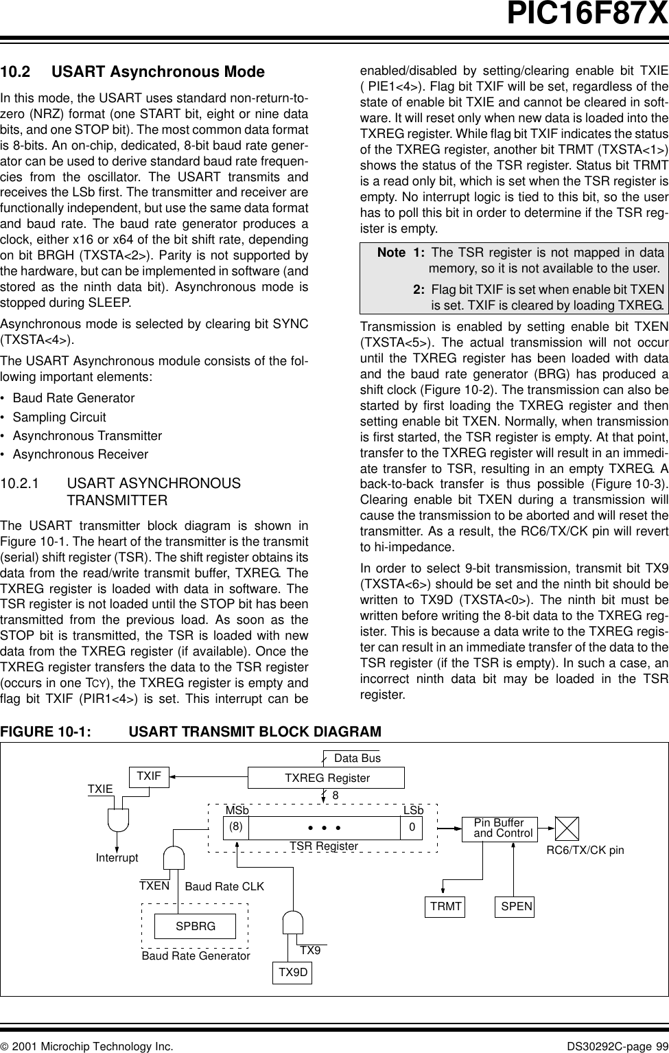
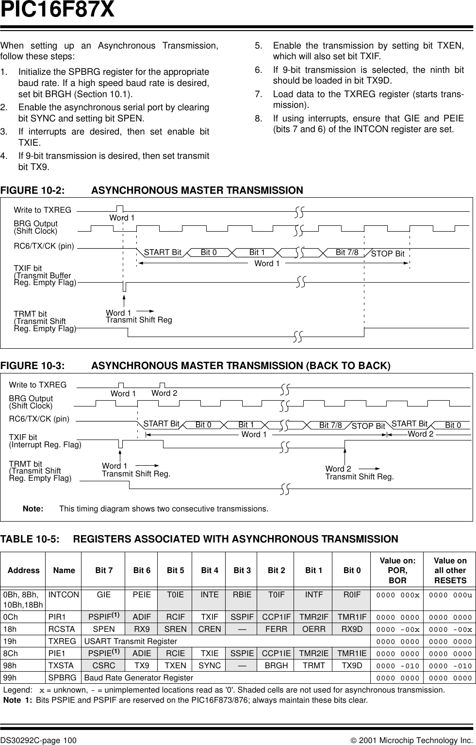
PIC16F87XDS30292C-page 80  2001 Microchip Technology Inc.FIGURE 9-11: BAUD RATE GENERATOR TIMING WITH CLOCK ARBITRATION        9.2.9 I2C MASTER MODE START CONDITION TIMINGTo initiate a START condition, the user sets the STARTcondition enable bit, SEN (SSPCON2<0>). If the SDAand SCL pins are sampled high, the baud rate genera-tor is reloaded with the contents of SSPADD<6:0> andstarts its count. If SCL and SDA are both sampled highwhen the baud rate generator times out (TBRG), theSDA pin is driven low. The action of the SDA beingdriven low while SCL is high is the START condition,and causes the S bit (SSPSTAT<3>) to be set. Follow-ing this, the baud rate generator is reloaded with thecontents of SSPADD<6:0> and resumes its count.When the baud rate generator times out (TBRG), theSEN bit (SSPCON2<0>) will be automatically clearedby hardware. The baud rate generator is suspended,leaving the SDA line held low, and the START conditionis complete.     9.2.9.1 WCOL Status FlagIf the user writes the SSPBUF when a STARTsequence is in progress, then WCOL is set and thecontents of the buffer are unchanged (the write doesn’toccur).    FIGURE 9-12: FIRST START BIT TIMING        SDASCLSCL de-asserted but slave holdsDX-1DXBRGSCL is sampled high, reload takesplace, and BRG starts its count03h 02h 01h 00h (hold off) 03h 02hReloadBRGValueSCL low (clock arbitration)SCL allowed to transition highBRG decrements(on Q2 and Q4 cycles)Note: If, at the beginning of START condition, theSDA and SCL pins are already sampledlow, or if during the START condition theSCL line is sampled low before the SDAline is driven low, a bus collision occurs,the Bus Collision Interrupt Flag (BCLIF) isset, the START condition is aborted, andthe I2C module is reset into its IDLE state.Note: Because queueing of events is notallowed, writing to the lower 5 bits ofSSPCON2 is disabled until the STARTcondition is complete.SDASCLSTBRG1st Bit 2nd BitTBRGSDA = 1,  At completion of START bit,SCL = 1Write to SSPBUF occurs hereTBRGHardware clears SEN bitTBRGWrite to SEN bit occurs here Set S bit (SSPSTAT<3>)    and sets SSPIF bit
 2001 Microchip Technology Inc. DS30292C-page 81PIC16F87X9.2.10 I2C MASTER MODE REPEATED START CONDITION TIMINGA Repeated START condition occurs when the RSENbit (SSPCON2<1>) is programmed high and the I2Cmodule is in the IDLE state. When the RSEN bit is set,the SCL pin is asserted low. When the SCL pin is sam-pled low, the baud rate generator is loaded with thecontents of SSPADD<6:0> and begins counting. TheSDA pin is released (brought high) for one baud rategenerator count (TBRG). When the baud rate generatortimes out, if SDA is sampled high, the SCL pin will bede-asserted (brought high). When SCL is sampled highthe baud rate generator is reloaded with the contents ofSSPADD<6:0> and begins counting. SDA and SCLmust be sampled high for one TBRG. This action is thenfollowed by assertion of the SDA pin (SDA is low) forone TBRG, while SCL is high. Following this, the RSENbit in the SSPCON2 register will be automaticallycleared and the baud rate generator will not bereloaded, leaving the SDA pin held low. As soon as aSTART condition is detected on the SDA and SCL pins,the S bit (SSPSTAT<3>) will be set. The SSPIF bit willnot be set until the baud rate generator has timed out.         Immediately following the SSPIF bit getting set, theuser may write the SSPBUF with the 7-bit address in7-bit mode, or the default first address in 10-bit mode.After the first eight bits are transmitted and an ACK isreceived, the user may then transmit an additional eightbits of address (10-bit mode), or eight bits of data (7-bitmode).9.2.10.1 WCOL Status FlagIf the user writes the SSPBUF when a RepeatedSTART sequence is in progress, then WCOL is set andthe contents of the buffer are unchanged (the writedoesn’t occur).      FIGURE 9-13: REPEAT START CONDITION WAVEFORM       Note 1: If RSEN is programmed while any otherevent is in progress, it will not take effect.2: A bus collision during the RepeatedSTART condition occurs if: •SDA is sampled low when SCL goes from low to high.•SCL goes low before SDA is asserted low. This may indicate that another master is attempting to transmit a data "1".Note: Because queueing of events is notallowed, writing of the lower 5 bits ofSSPCON2 is disabled until the RepeatedSTART condition is complete.SDASCLSr = Repeated STARTWrite to SSPCON2 Write to SSPBUF occurs hereFalling edge of ninth clockEnd of XmitAt completion of START bit, hardware clears RSEN bit1st bitSet S (SSPSTAT<3>)TBRGTBRGSDA = 1,SDA = 1, SCL (no change)SCL = 1occurs hereTBRG TBRG TBRG     and sets SSPIF
PIC16F87XDS30292C-page 82  2001 Microchip Technology Inc.9.2.11 I2C MASTER MODE TRANSMISSIONTransmission of a data byte, a 7-bit address, or eitherhalf of a 10-bit address, is accomplished by simply writ-ing a value to SSPBUF register. This action will set theBuffer Full flag (BF) and allow the baud rate generatorto begin counting and start the next transmission. Eachbit of address/data will be shifted out onto the SDA pinafter the falling edge of SCL is asserted (see data holdtime spec).  SCL is held low for one baud rate generatorrollover count (TBRG). Data should be valid before SCLis released high (see data setup time spec). When theSCL pin is released high, it is held that way for TBRG.The data on the SDA pin must remain stable for thatduration and some hold time after the next falling edgeof SCL. After the eighth bit is shifted out (the fallingedge of the eighth clock), the BF flag is cleared and themaster releases SDA allowing the slave device beingaddressed to respond with an ACK bit during the ninthbit time, if an address match occurs or if data wasreceived properly. The status of ACK is read into theACKDT on the falling edge of the ninth clock. If themaster receives an Acknowledge, the AcknowledgeStatus bit (ACKSTAT) is cleared. If not, the bit is set.After the ninth clock, the SSPIF is set and the masterclock (baud rate generator) is suspended until the nextdata byte is loaded into the SSPBUF, leaving SCL lowand SDA unchanged (Figure 9-14).After the write to the SSPBUF, each bit of address willbe shifted out on the falling edge of SCL, until all sevenaddress bits and the R/W bit are completed. On the fall-ing edge of the eighth clock, the master will de-assertthe SDA pin, allowing the slave to respond with anAcknowledge. On the falling edge of the ninth clock, themaster will sample the SDA pin to see if the addresswas recognized by a slave. The status of the ACK bit isloaded into the ACKSTAT status bit (SSPCON2<6>).Following the falling edge of the ninth clock transmis-sion of the address, the SSPIF is set, the BF flag iscleared, and the baud rate generator is turned off untilanother write to the SSPBUF takes place, holding SCLlow and allowing SDA to float.9.2.11.1 BF Status FlagIn Transmit mode, the BF bit (SSPSTAT<0>) is setwhen the CPU writes to SSPBUF and is cleared whenall 8 bits are shifted out.9.2.11.2 WCOL Status FlagIf the user writes the SSPBUF when a transmit isalready in progress (i.e., SSPSR is still shifting out adata byte), then WCOL is set and the contents of thebuffer are unchanged (the write doesn’t occur). WCOL must be cleared in software.9.2.11.3 ACKSTAT Status FlagIn Transmit mode, the ACKSTAT bit (SSPCON2<6>) iscleared when the slave has sent an Acknowledge(ACK = 0), and is set when the slave does not Acknowl-edge (ACK = 1). A slave sends an Acknowledge whenit has recognized its address (including a general call),or when the slave has properly received its data.
 2001 Microchip Technology Inc. DS30292C-page 83PIC16F87XFIGURE 9-14: I2C MASTER MODE TIMING (TRANSMISSION, 7 OR 10-BIT ADDRESS)       SDASCLSSPIF BF (SSPSTAT<0>)SENA7 A6 A5 A4 A3 A2 A1 ACK = 0 D7D6D5D4D3D2D1D0ACKTransmitting Data or Second HalfR/W = 0Transmit Address to Slave123456789 123456789 PCleared in software service routineSSPBUF is written in softwareFrom SSP interruptAfter START condition SEN, cleared by hardware.SSSPBUF written with 7-bit address and R/Wstart transmitSCL held lowwhile CPUresponds to SSPIFSEN = 0of 10-bit addressWrite SSPCON2<0> SEN = 1START condition begins From slave clear ACKSTAT bit SSPCON2<6>ACKSTAT in SSPCON2 = 1Cleared in softwareSSPBUF writtenPENCleared in softwareR/W
PIC16F87XDS30292C-page 84  2001 Microchip Technology Inc.9.2.12 I2C MASTER MODE RECEPTIONMaster mode reception is enabled by programming theReceive Enable bit, RCEN (SSPCON2<3>).       The baud rate generator begins counting, and on eachrollover, the state of the SCL pin changes (high to low/low to high), and data is shifted into the SSPSR. Afterthe falling edge of the eighth clock, the receive enableflag is automatically cleared, the contents of theSSPSR are loaded into the SSPBUF, the BF flag is set,the SSPIF is set, and the baud rate generator is sus-pended from counting, holding SCL low. The SSP isnow in IDLE state, awaiting the next command. Whenthe buffer is read by the CPU, the BF flag is automati-cally cleared. The user can then send an Acknowledgebit at the end of reception, by setting the AcknowledgeSequence Enable bit, ACKEN (SSPCON2<4>).9.2.12.1 BF Status FlagIn receive operation, BF is set when an address or databyte is loaded into SSPBUF from SSPSR. It is clearedwhen SSPBUF is read.9.2.12.2 SSPOV Status FlagIn receive operation, SSPOV is set when 8 bits arereceived into the SSPSR, and the BF flag is already setfrom a previous reception.9.2.12.3 WCOL Status FlagIf the user writes the SSPBUF when a receive isalready in progress (i.e., SSPSR is still shifting in a databyte), then WCOL is set and the contents of the bufferare unchanged (the write doesn’t occur).Note: The SSP module must be in an IDLE statebefore the RCEN bit is set, or the RCEN bitwill be disregarded.
 2001 Microchip Technology Inc. DS30292C-page 85PIC16F87XFIGURE 9-15: I2C MASTER MODE TIMING (RECEPTION, 7-BIT ADDRESS)          P98765D0D1D2D3D4D5D6D7SA7 A6 A5 A4 A3 A2 A1SDASCL 12345678912345678 9 1234Bus MasterterminatestransferACKReceiving Data from SlaveReceiving Data from SlaveD0D1D2D3D4D5D6D7ACKR/W = 1Transmit Address to SlaveSSPIFBF ACK is not sentWrite to SSPCON2<0> (SEN = 1)Write to SSPBUF occurs here ACK from SlaveMaster configured as a receiverby programming SSPCON2<3>, (RCEN = 1) PEN bit = 1written hereData shifted in on falling edge of CLKCleared in softwareStart XMITSEN = 0SSPOVSDA = 0, SCL = 1while CPU (SSPSTAT<0>)ACKLast bit is shifted into SSPSR andcontents are unloaded into SSPBUFCleared in softwareCleared in softwareSet SSPIF interruptat end of receiveSet P bit (SSPSTAT<4>)and SSPIFCleared insoftwareACK from MasterSet SSPIF at endSet SSPIF interruptat end of acknowledgesequenceSet SSPIF interruptat end of Acknow-ledge sequenceof receiveSet ACKEN to start Acknowledge sequenceSSPOV is set becauseSSPBUF is still fullSDA = ACKDT = 1 RCEN clearedautomaticallyRCEN = 1 startnext receiveWrite to SSPCON2<4>to start Acknowledge sequenceSDA = ACKDT (SSPCON2<5>) = 0RCEN clearedautomaticallyresponds to SSPIFACKENBegin START ConditionCleared in softwareSDA = ACKDT = 0
PIC16F87XDS30292C-page 86  2001 Microchip Technology Inc.9.2.13 ACKNOWLEDGE SEQUENCE TIMINGAn Acknowledge sequence is enabled by setting theAcknowledge Sequence Enable bit, ACKEN(SSPCON2<4>). When this bit is set, the SCL pin ispulled low and the contents of the Acknowledge data bitis presented on the SDA pin. If the user wishes to gen-erate an Acknowledge, the ACKDT bit should becleared. If not, the user should set the ACKDT bitbefore starting an Acknowledge sequence. The baudrate generator then counts for one rollover period(TBRG), and the SCL pin is de-asserted high. When theSCL pin is sampled high (clock arbitration), the baudrate generator counts for TBRG. The SCL pin is thenpulled low. Following this, the ACKEN bit is automati-cally cleared, the baud rate generator is turned off,and the SSP module then goes into IDLE mode(Figure 9-16).9.2.13.1 WCOL Status FlagIf the user writes the SSPBUF when an Acknowledgesequence is in progress, the WCOL is set and the con-tents of the buffer are unchanged (the write doesn’toccur).FIGURE 9-16: ACKNOWLEDGE SEQUENCE WAVEFORM         Note:  TBRG = one baud rate generator period.SDASCLSet SSPIF at the endAcknowledge sequence starts here,Write to SSPCON2 ACKEN automatically clearedCleared inTBRG TBRGof receiveACK8ACKEN = 1, ACKDT = 0D09SSPIFsoftwareSet SSPIF at the endof Acknowledge sequenceCleared insoftware
 2001 Microchip Technology Inc. DS30292C-page 87PIC16F87X9.2.14 STOP CONDITION TIMINGA STOP bit is asserted on the SDA pin at the end of areceive/transmit by setting the Stop Sequence Enablebit, PEN (SSPCON2<2>). At the end of a receive/transmit, the SCL line is held low after the falling edgeof the ninth clock. When the PEN bit is set, the masterwill assert the SDA line low. When the SDA line is sam-pled low, the baud rate generator is reloaded andcounts down to 0. When the baud rate generator timesout, the SCL pin will be brought high, and one TBRG(baud rate generator rollover count) later, the SDA pinwill be de-asserted. When the SDA pin is sampled highwhile SCL is high, the P bit (SSPSTAT<4>) is set. ATBRG later, the PEN bit is cleared and the SSPIF bit isset (Figure 9-17).Whenever the firmware decides to take control of thebus, it will first determine if the bus is busy by checkingthe S and P bits in the SSPSTAT register. If the bus isbusy, then the CPU can be interrupted (notified) whena STOP bit is detected (i.e., bus is free).9.2.14.1 WCOL Status FlagIf the user writes the SSPBUF when a STOP sequenceis in progress, then WCOL is set and the contents of thebuffer are unchanged (the write doesn’t occur).FIGURE 9-17: STOP CONDITION RECEIVE OR TRANSMIT MODE       SCLSDASDA asserted low before rising edge of clockWrite to SSPCON2Set PENFalling edge ofSCL = 1 for TBRG, followed by SDA = 1 for TBRG9th clockSCL brought high after TBRGNote:  TBRG = one baud rate generator period.TBRG TBRGafter SDA sampled high. P bit (SSPSTAT<4>) is set. TBRGto setup STOP conditionACKPTBRGPEN bit (SSPCON2<2>) is cleared by   hardware and the SSPIF bit is set
PIC16F87XDS30292C-page 88  2001 Microchip Technology Inc.9.2.15 CLOCK ARBITRATIONClock arbitration occurs when the master, during anyreceive, transmit, or Repeated START/STOP condi-tion, de-asserts the SCL pin (SCL allowed to float high).When the SCL pin is allowed to float high, the baud rategenerator (BRG) is suspended from counting until theSCL pin is actually sampled high. When the SCL pin issampled high, the baud rate generator is reloaded withthe contents of SSPADD<6:0> and begins counting.This ensures that the SCL high time will always be atleast one BRG rollover count in the event that the clockis held low by an external device (Figure 9-18).9.2.16 SLEEP OPERATIONWhile in SLEEP mode, the I2C module can receiveaddresses or data, and when an address match orcomplete byte transfer occurs, wake the processorfrom SLEEP (if the SSP interrupt is enabled).9.2.17 EFFECTS OF A RESETA RESET disables the SSP module and terminates thecurrent transfer.FIGURE 9-18: CLOCK ARBITRATION TIMING IN MASTER TRANSMIT MODE      SCLSDABRG overflow,Release SCL,If SCL = 1, Load BRG withSSPADD<6:0>, and start count BRG overflow occurs,Release SCL, Slave device holds SCL low SCL = 1, BRG starts countingclock high intervalSCL line sampled once every machine cycle (TOSC • 4).Hold off BRG until SCL is sampled high.TBRG TBRG TBRGto measure high time interval
 2001 Microchip Technology Inc. DS30292C-page 89PIC16F87X9.2.18 MULTI -MASTER COMMUNICATION, BUS COLLISION, AND BUS ARBITRATIONMulti-Master mode support is achieved by bus arbitra-tion. When the master outputs address/data bits ontothe SDA pin, arbitration takes place when the masteroutputs a ’1’ on SDA, by letting SDA float high andanother master asserts a ’0’.   When the SCL pin floatshigh, data should be stable. If the expected data onSDA is a ’1’ and the data sampled on the SDA pin = ’0’,a bus collision has taken place. The master will set theBus Collision Interrupt Flag, BCLIF and reset the I2Cport to its IDLE state (Figure 9-19).If a transmit was in progress when the bus collisionoccurred, the transmission is halted, the BF flag iscleared, the SDA and SCL lines are de-asserted, andthe SSPBUF can be written to. When the user servicesthe bus collision Interrupt Service Routine, and if theI2C bus is free, the user can resume communication byasserting a START condition. If a START, Repeated START, STOP, or Acknowledgecondition was in progress when the bus collisionoccurred, the condition is aborted, the SDA and SCLlines are de-asserted, and the respective control bits inthe SSPCON2 register are cleared. When the user ser-vices the bus collision Interrupt Service Routine, and ifthe I2C bus is free, the user can resume communicationby asserting a START condition.The master will continue to monitor the SDA and SCLpins and if a STOP condition occurs, the SSPIF bit willbe set.A write to the SSPBUF will start the transmission ofdata at the first data bit, regardless of where the trans-mitter left off when the bus collision occurred.In Multi-Master mode, the interrupt generation on thedetection of START and STOP conditions allows thedetermination of when the bus is free. Control of the I2Cbus can be taken when the P bit is set in the SSPSTATregister, or the bus is idle and the S and P bits arecleared.FIGURE 9-19: BUS COLLISION TIMING FOR TRANSMIT AND ACKNOWLEDGE       SDASCLBCLIFSDA released SDA line pulled lowby another sourceSample SDA. While SCL is high,data doesn’t match what is driven Bus collision has occurred.Set bus collisioninterruptby the master.by masterData changeswhile SCL = 0
PIC16F87XDS30292C-page 90  2001 Microchip Technology Inc.9.2.18.1 Bus Collision During a START ConditionDuring a START condition, a bus collision occurs if:a) SDA or SCL are sampled low at the beginning ofthe START condition (Figure 9-20).b) SCL is sampled low before SDA is asserted low(Figure 9-21).During a START condition, both the SDA and the SCLpins are monitored. If either the SDA pin or the SCL pinis already low, then these events all occur:•the START condition is aborted, •and the BCLIF flag is set,•and the SSP module is reset to its IDLE state (Figure 9-20).The START condition begins with the SDA and SCLpins de-asserted. When the SDA pin is sampled high,the baud rate generator is loaded from SSPADD<6:0>and counts down to 0. If the SCL pin is sampled lowwhile SDA is high, a bus collision occurs, because it isassumed that another master is attempting to drive adata '1' during the START condition. If the SDA pin is sampled low during this count, theBRG is reset and the SDA line is asserted early(Figure 9-22). If, however, a '1' is sampled on the SDApin, the SDA pin is asserted low at the end of the BRGcount. The baud rate generator is then reloaded andcounts down to 0. During this time, if the SCL pins aresampled as '0', a bus collision does not occur. At theend of the BRG count, the SCL pin is asserted low.      FIGURE 9-20: BUS COLLISION DURING START CONDITION (SDA ONLY)      Note: The reason that bus collision is not a factorduring a START condition is that no twobus masters can assert a START conditionat the exact same time. Therefore, onemaster will always assert SDA before theother. This condition does not cause a buscollision, because the two masters must beallowed to arbitrate the first address follow-ing the START condition. If the address isthe same, arbitration must be allowed tocontinue into the data portion, RepeatedSTART, or STOP conditions.SDASCLSENSDA sampled low before SDA goes low before the SEN bit is set.S bit and SSPIF set becauseSSP module reset into IDLE state.SEN cleared automatically because of bus collision. S bit and SSPIF set becauseSet SEN, enable STARTcondition if SDA = 1, SCL = 1SDA = 0, SCL = 1.BCLIFSSSPIFSDA = 0, SCL = 1.SSPIF and BCLIF arecleared in softwareSSPIF and BCLIF arecleared in softwareSet BCLIF, Set BCLIF.START condition.
 2001 Microchip Technology Inc. DS30292C-page 91PIC16F87XFIGURE 9-21: BUS COLLISION DURING START CONDITION (SCL = 0)      FIGURE 9-22: BRG RESET DUE TO SDA COLLISION DURING START CONDITION        SDASCLSEN Bus collision occurs, Set BCLIFSCL = 0 before SDA = 0,Set SEN, enable STARTsequence if SDA = 1, SCL = 1TBRG TBRGSDA = 0, SCL = 1BCLIFSSSPIFInterrupts clearedin softwareBus collision occurs, Set BCLIFSCL = 0 before BRG time-out,’0’’0’’0’’0’SDASCLSENSet SSet SEN, enable STARTsequence if SDA = 1, SCL = 1Less than TBRG TBRGSDA = 0, SCL = 1BCLIFSSSPIFsInterrupts clearedin softwareSet SSPIFSDA = 0, SCL = 1SDA pulled low by other master.Reset BRG and assert SDA.SCL pulled low after BRGTime-outSet SSPIF’0’
PIC16F87XDS30292C-page 92  2001 Microchip Technology Inc.9.2.18.2 Bus Collision During a Repeated START ConditionDuring a Repeated START condition, a bus collisionoccurs if: a) A low level is sampled on SDA when SCL goesfrom low level to high level.b) SCL goes low before SDA is asserted low, indi-cating that another master is attempting to trans-mit a data ’1’.When the user de-asserts SDA and the pin is allowedto float high, the BRG is loaded with SSPADD<6:0>and counts down to 0. The SCL pin is then de-asserted,and when sampled high, the SDA pin is sampled. IfSDA is low, a bus collision has occurred (i.e., anothermaster is attempting to transmit a data’0’). If, however,SDA is sampled high, the BRG is reloaded and beginscounting. If SDA goes from high to low before the BRGtimes out, no bus collision occurs, because no twomasters can assert SDA at exactly the same time. If, however, SCL goes from high to low before the BRGtimes out and SDA has not already been asserted, abus collision occurs. In this case, another master isattempting to transmit a data’1’ during the RepeatedSTART condition.If at the end of the BRG time-out, both SCL and SDAare still high, the SDA pin is driven low, the BRG isreloaded and begins counting. At the end of the count,regardless of the status of the SCL pin, the SCL pin isdriven low and the Repeated START condition iscomplete (Figure 9-23).FIGURE 9-23: BUS COLLISION DURING A REPEATED START CONDITION (CASE 1)        FIGURE 9-24: BUS COLLISION DURING REPEATED START CONDITION (CASE 2)      SDASCLRSENBCLIFSSSPIFSample SDA when SCL goes high.If SDA = 0, set BCLIF and release SDA and SCL.Cleared in software’0’’0’’0’’0’SDASCLBCLIFRSENSSSPIFInterrupt clearedin softwareSCL goes low before SDA,Set BCLIF. Release SDA and SCL.TBRG TBRG’0’’0’’0’’0’
 2001 Microchip Technology Inc. DS30292C-page 93PIC16F87X9.2.18.3 Bus Collision During a STOP ConditionBus collision occurs during a STOP condition if:a) After the SDA pin has been de-asserted andallowed to float high, SDA is sampled low afterthe BRG has timed out.b) After the SCL pin is de-asserted, SCL is sam-pled low before SDA goes high.The STOP condition begins with SDA asserted low.When SDA is sampled low, the SCL pin is allowed tofloat. When the pin is sampled high (clock arbitration),the baud rate generator is loaded with SSPADD<6:0>and counts down to 0. After the BRG times out, SDA issampled. If SDA is sampled low, a bus collision hasoccurred. This is due to another master attempting todrive a data ’0’. If the SCL pin is sampled low beforeSDA is allowed to float high, a bus collision occurs. Thisis a case of another master attempting to drive a data’0’ (Figure 9-25).FIGURE 9-25: BUS COLLISION DURING A STOP CONDITION (CASE 1)      FIGURE 9-26:  BUS COLLISION DURING A STOP CONDITION (CASE 2)      SDASCLBCLIFPENPSSPIFTBRG TBRG TBRGSDA asserted lowSDA sampledlow after TBRG,Set BCLIF’0’’0’’0’’0’SDASCLBCLIFPENPSSPIFTBRG TBRG TBRGAssert SDA SCL goes low before SDA goes high,Set BCLIF’0’’0’
PIC16F87XDS30292C-page 94  2001 Microchip Technology Inc.9.3 Connection Considerations for I2C BusFor standard-mode I2C bus devices, the values ofresistors Rp and Rs in Figure 9-27 depend on the fol-lowing parameters:•Supply voltage•Bus capacitance•Number of connected devices (input current + leakage current)The supply voltage limits the minimum value of resistorRp, due to the specified minimum sink current of 3 mA atVOL max = 0.4V, for the specified output stages. Forexample, with a supply voltage of VDD = 5V±10% andVOL max = 0.4V at 3 mA, Rp min = (5.5-0.4)/0.003 = 1.7 kΩ.VDD as a function of Rp is shown in Figure 9-27. Thedesired noise margin of 0.1VDD for the low level limitsthe maximum value of Rs. Series resistors are optionaland used to improve ESD susceptibility.The bus capacitance is the total capacitance of wire,connections, and pins. This capacitance limits the max-imum value of Rp due to the specified rise time(Figure 9-27).The SMP bit is the slew rate control enabled bit. This bitis in the SSPSTAT register, and controls the slew rateof the I/O pins when in I2C mode (master or slave).FIGURE 9-27: SAMPLE DEVICE CONFIGURATION FOR I2C BUS       RpRpVDD  + 10%SDASCLDEVICECb=10 - 400 pFRsRsNote: I2C devices with input levels related to VDD must have one common supply line to which the pull-up resistor is alsoconnected.
 2001 Microchip Technology Inc. DS30292C-page 95PIC16F87X10.0 ADDRESSABLE UNIVERSAL SYNCHRONOUS ASYNCHRONOUS RECEIVER TRANSMITTER (USART) The Universal Synchronous Asynchronous ReceiverTransmitter (USART) module is one of the two serialI/O modules. (USART is also known as a Serial Com-munications Interface or SCI.) The USART can be con-figured as a full duplex asynchronous system that cancommunicate with peripheral devices such as CRT ter-minals and personal computers, or it can be configuredas a half duplex synchronous system that can commu-nicate with peripheral devices such as A/D or D/A inte-grated circuits, serial EEPROMs etc.The USART can be configured in the following modes:•Asynchronous (full duplex)•Synchronous - Master (half duplex)•Synchronous - Slave (half duplex)Bit SPEN (RCSTA<7>) and bits TRISC<7:6> have tobe set in order to configure pins RC6/TX/CK andRC7/RX/DT as the Universal Synchronous Asynchro-nous Receiver Transmitter.The USART module also has a multi-processor com-munication capability using 9-bit address detection.REGISTER 10-1: TXSTA: TRANSMIT STATUS AND CONTROL REGISTER (ADDRESS 98h)                      R/W-0 R/W-0 R/W-0 R/W-0 U-0 R/W-0 R-1 R/W-0CSRC TX9 TXEN SYNC —BRGH TRMT TX9Dbit 7 bit 0bit 7 CSRC: Clock Source Select bitAsynchronous mode:Don’t careSynchronous mode:1 = Master mode (clock generated internally from BRG)0 = Slave mode (clock from external source)bit 6 TX9: 9-bit Transmit Enable bit1 = Selects 9-bit transmission0 = Selects 8-bit transmissionbit 5  TXEN: Transmit Enable bit1 = Transmit enabled0 = Transmit disabledNote: SREN/CREN overrides TXEN in SYNC mode.bit 4  SYNC: USART Mode Select bit1 = Synchronous mode0 = Asynchronous modebit 3 Unimplemented: Read as '0'bit 2 BRGH: High Baud Rate Select bitAsynchronous mode:1 = High speed0 = Low speedSynchronous mode:Unused in this modebit 1 TRMT: Transmit Shift Register Status bit1 = TSR empty0 = TSR fullbit 0 TX9D: 9th bit of Transmit Data, can be parity bitLegend:R = Readable bit W = Writable bit U = Unimplemented bit, read as ‘0’- n = Value at POR ’1’ = Bit is set ’0’ = Bit is cleared x = Bit is unknown
PIC16F87XDS30292C-page 96  2001 Microchip Technology Inc.REGISTER 10-2: RCSTA: RECEIVE STATUS AND CONTROL REGISTER (ADDRESS 18h)                      R/W-0 R/W-0 R/W-0 R/W-0 R/W-0 R-0 R-0 R-xSPEN RX9 SREN CREN ADDEN FERR OERR RX9Dbit 7 bit 0bit 7 SPEN: Serial Port Enable bit1 = Serial port enabled (configures RC7/RX/DT and RC6/TX/CK pins as serial port pins)0 = Serial port disabledbit 6 RX9: 9-bit Receive Enable bit1 = Selects 9-bit reception0 = Selects 8-bit receptionbit 5 SREN: Single Receive Enable bitAsynchronous mode:Don’t careSynchronous mode - master:1 = Enables single receive0 = Disables single receiveThis bit is cleared after reception is complete.Synchronous mode - slave:Don’t carebit 4 CREN: Continuous Receive Enable bitAsynchronous mode:1 = Enables continuous receive0 = Disables continuous receiveSynchronous mode:1 = Enables continuous receive until enable bit CREN is cleared (CREN overrides SREN)0 = Disables continuous receivebit 3 ADDEN: Address Detect Enable bitAsynchronous mode 9-bit (RX9 = 1):1 = Enables address detection, enables interrupt and load of the receive buffer when RSR<8> is set0 = Disables address detection, all bytes are received, and ninth bit can be used as parity bitbit 2 FERR: Framing Error bit1 = Framing error (can be updated by reading RCREG register and receive next valid byte)0 = No framing errorbit 1  OERR: Overrun Error bit1 = Overrun error (can be cleared by clearing bit CREN)0 = No overrun errorbit 0  RX9D: 9th bit of Received Data (can be parity bit, but must be calculated by user firmware)Legend:R = Readable bit W = Writable bit U = Unimplemented bit, read as ‘0’- n = Value at POR ’1’ = Bit is set ’0’ = Bit is cleared x = Bit is unknown
 2001 Microchip Technology Inc. DS30292C-page 97PIC16F87X10.1 USART Baud Rate Generator (BRG)The BRG supports both the Asynchronous and Syn-chronous modes of the USART. It is a dedicated 8-bitbaud rate generator. The SPBRG register controls theperiod of a free running 8-bit timer. In Asynchronousmode, bit BRGH (TXSTA<2>) also controls the baudrate. In Synchronous mode, bit BRGH is ignored.Table 10-1 shows the formula for computation of thebaud rate for different USART modes which only applyin Master mode (internal clock).Given the desired baud rate and FOSC, the nearestinteger value for the SPBRG register can be calculatedusing the formula in Table 10-1. From this, the error inbaud rate can be determined. It may be advantageous to use the high baud rate(BRGH = 1), even for slower baud clocks. This isbecause the FOSC/(16(X + 1)) equation can reduce thebaud rate error in some cases.Writing a new value to the SPBRG register causes theBRG timer to be reset (or cleared). This ensures theBRG does not wait for a timer overflow before output-ting the new baud rate. 10.1.1 SAMPLINGThe data on the RC7/RX/DT pin is sampled three timesby a majority detect circuit to determine if a high or alow level is present at the RX pin. TABLE 10-1: BAUD RATE FORMULATABLE 10-2: REGISTERS ASSOCIATED WITH BAUD RATE GENERATORSYNC BRGH = 0 (Low Speed) BRGH = 1 (High Speed)01(Asynchronous) Baud Rate = FOSC/(64(X+1))(Synchronous) Baud Rate = FOSC/(4(X+1)) Baud Rate = FOSC/(16(X+1))N/AX = value in SPBRG (0 to 255)Address Name Bit 7 Bit 6 Bit 5 Bit 4 Bit 3 Bit 2 Bit 1 Bit 0 Value on: POR,BORValue on all other RESETS98h TXSTA CSRC TX9 TXEN SYNC —BRGH TRMT TX9D 0000 -010 0000 -01018h RCSTA SPEN RX9 SREN CREN ADDEN FERR OERR RX9D 0000 000x 0000 000x99h SPBRG Baud Rate Generator Register 0000 0000 0000 0000Legend: x = unknown, - = unimplemented, read as '0'. Shaded cells are not used by the BRG.
PIC16F87XDS30292C-page 98  2001 Microchip Technology Inc.TABLE 10-3: BAUD RATES FOR ASYNCHRONOUS MODE (BRGH = 0)BAUDRATE(K) FOSC = 20 MHz FOSC = 16 MHz FOSC = 10 MHzKBAUD %ERRORSPBRGvalue (decimal) KBAUD %ERRORSPBRGvalue (decimal) KBAUD %ERRORSPBRGvalue (decimal)0.3------- --1.2 1.221 1.75 255 1.202 0.17 207 1.202 0.17 1292.4 2.404 0.17 129 2.404 0.17 103 2.404 0.17 649.6 9.766 1.73 31 9.615 0.16 25 9.766 1.73 1519.2 19.531  1.72 15 19.231 0.16 12 19.531 1.72 728.8 31.250 8.51 9 27.778 3.55 8 31.250 8.51 433.6 34.722 3.34 8 35.714 6.29 6 31.250 6.99 457.6 62.500 8.51 4 62.500 8.51 3 52.083 9.58 2HIGH 1.221 - 255 0.977 - 255 0.610 - 255LOW 312.500 - 0 250.000 - 0 156.250 - 0BAUDRATE(K) FOSC = 4 MHz FOSC = 3.6864 MHzKBAUD%ERRORSPBRGvalue (decimal) KBAUD%ERRORSPBRGvalue (decimal)0.3 0.300 0 207 0.3 0 1911.2 1.202 0.17 51 1.2 0 472.4 2.404 0.17 25 2.4 0 239.6 8.929 6.99 6 9.6 0 519.2 20.833 8.51 2 19.2 0 228.8 31.250 8.51 1 28.8 0 133.6 - - - - - -57.6 62.500 8.51 0 57.6 0 0HIGH 0.244 - 255 0.225 - 255LOW 62.500 - 0 57.6 - 0TABLE 10-4: BAUD RATES FOR ASYNCHRONOUS MODE (BRGH = 1)BAUDRATE(K) FOSC = 20 MHz FOSC = 16 MHz FOSC = 10 MHzKBAUD %ERRORSPBRGvalue (decimal) KBAUD %ERRORSPBRGvalue (decimal) KBAUD %ERRORSPBRGvalue (decimal)0.3---------1.2---------2.4 - - - - - - 2.441 1.71 2559.6 9.615 0.16 129 9.615 0.16 103 9.615 0.16 6419.2 19.231 0.16 64 19.231 0.16 51 19.531 1.72 3128.8 29.070 0.94 42 29.412 2.13 33 28.409 1.36 2133.6 33.784 0.55 36 33.333 0.79 29 32.895 2.10 1857.6 59.524 3.34 20 58.824 2.13 16 56.818 1.36 10HIGH 4.883 - 255 3.906 - 255 2.441 - 255LOW 1250.000 - 0 1000.000 0 625.000 - 0BAUDRATE(K) FOSC = 4 MHz FOSC = 3.6864 MHzKBAUD%ERRORSPBRGvalue (decimal) KBAUD%ERRORSPBRGvalue (decimal)0.3------1.2 1.202 0.17 207 1.2 0 1912.4 2.404 0.17 103 2.4 0 959.6 9.615 0.16 25 9.6 0 2319.2 19.231 0.16 12 19.2 0 1128.8 27.798 3.55 8 28.8 0 733.6 35.714 6.29 6 32.9 2.04 657.6 62.500 8.51 3 57.6 0 3HIGH 0.977 - 255 0.9 - 255LOW 250.000 - 0 230.4 - 0
 2001 Microchip Technology Inc. DS30292C-page 99PIC16F87X10.2 USART Asynchronous ModeIn this mode, the USART uses standard non-return-to-zero (NRZ) format (one START bit, eight or nine databits, and one STOP bit). The most common data formatis 8-bits. An on-chip, dedicated, 8-bit baud rate gener-ator can be used to derive standard baud rate frequen-cies from the oscillator. The USART transmits andreceives the LSb first. The transmitter and receiver arefunctionally independent, but use the same data formatand baud rate. The baud rate generator produces aclock, either x16 or x64 of the bit shift rate, dependingon bit BRGH (TXSTA<2>). Parity is not supported bythe hardware, but can be implemented in software (andstored as the ninth data bit). Asynchronous mode isstopped during SLEEP.Asynchronous mode is selected by clearing bit SYNC(TXSTA<4>). The USART Asynchronous module consists of the fol-lowing important elements:•Baud Rate Generator•Sampling Circuit•Asynchronous Transmitter•Asynchronous Receiver10.2.1 USART ASYNCHRONOUS TRANSMITTERThe USART transmitter block diagram is shown inFigure 10-1. The heart of the transmitter is the transmit(serial) shift register (TSR). The shift register obtains itsdata from the read/write transmit buffer, TXREG. TheTXREG register is loaded with data in software. TheTSR register is not loaded until the STOP bit has beentransmitted from the previous load. As soon as theSTOP bit is transmitted, the TSR is loaded with newdata from the TXREG register (if available). Once theTXREG register transfers the data to the TSR register(occurs in one TCY), the TXREG register is empty andflag bit TXIF (PIR1<4>) is set. This interrupt can beenabled/disabled by setting/clearing enable bit TXIE( PIE1<4>). Flag bit TXIF will be set, regardless of thestate of enable bit TXIE and cannot be cleared in soft-ware. It will reset only when new data is loaded into theTXREG register. While flag bit TXIF indicates the statusof the TXREG register, another bit TRMT (TXSTA<1>)shows the status of the TSR register. Status bit TRMTis a read only bit, which is set when the TSR register isempty. No interrupt logic is tied to this bit, so the userhas to poll this bit in order to determine if the TSR reg-ister is empty.Transmission is enabled by setting enable bit TXEN(TXSTA<5>). The actual transmission will not occuruntil the TXREG register has been loaded with dataand the baud rate generator (BRG) has produced ashift clock (Figure 10-2). The transmission can also bestarted by first loading the TXREG register and thensetting enable bit TXEN. Normally, when transmissionis first started, the TSR register is empty. At that point,transfer to the TXREG register will result in an immedi-ate transfer to TSR, resulting in an empty TXREG. Aback-to-back transfer is thus possible (Figure 10-3).Clearing enable bit TXEN during a transmission willcause the transmission to be aborted and will reset thetransmitter. As a result, the RC6/TX/CK pin will revertto hi-impedance.In order to select 9-bit transmission, transmit bit TX9(TXSTA<6>) should be set and the ninth bit should bewritten to TX9D (TXSTA<0>). The ninth bit must bewritten before writing the 8-bit data to the TXREG reg-ister. This is because a data write to the TXREG regis-ter can result in an immediate transfer of the data to theTSR register (if the TSR is empty). In such a case, anincorrect ninth data bit may be loaded in the TSRregister.FIGURE 10-1: USART TRANSMIT BLOCK DIAGRAMNote 1: The TSR register is not mapped in datamemory, so it is not available to the user.2: Flag bit TXIF is set when enable bit TXENis set. TXIF is cleared by loading TXREG.TXIFTXIEInterruptTXEN Baud Rate CLKSPBRGBaud Rate GeneratorTX9DMSb LSbData BusTXREG RegisterTSR Register(8) 0TX9TRMT SPENRC6/TX/CK pinPin Bufferand Control8•   •   •
PIC16F87XDS30292C-page 100  2001 Microchip Technology Inc.When setting up an Asynchronous Transmission,follow these steps:1. Initialize the SPBRG register for the appropriatebaud rate. If a high speed baud rate is desired,set bit BRGH (Section 10.1).2. Enable the asynchronous serial port by clearingbit SYNC and setting bit SPEN.3. If interrupts are desired, then set enable bitTXIE.4. If 9-bit transmission is desired, then set transmitbit TX9.5. Enable the transmission by setting bit TXEN,which will also set bit TXIF.6. If 9-bit transmission is selected, the ninth bitshould be loaded in bit TX9D.7. Load data to the TXREG register (starts trans-mission).8. If using interrupts, ensure that GIE and PEIE(bits 7 and 6) of the INTCON register are set.FIGURE 10-2: ASYNCHRONOUS MASTER TRANSMISSIONFIGURE 10-3: ASYNCHRONOUS MASTER TRANSMISSION (BACK TO BACK)TABLE 10-5: REGISTERS ASSOCIATED WITH ASYNCHRONOUS TRANSMISSIONAddress Name Bit 7 Bit 6 Bit 5 Bit 4 Bit 3 Bit 2 Bit 1 Bit 0 Value on:POR,BORValue onall otherRESETS0Bh, 8Bh, 10Bh,18BhINTCON GIE PEIE T0IE INTE RBIE T0IF INTF R0IF 0000 000x 0000 000u0Ch PIR1 PSPIF(1) ADIF RCIF TXIF SSPIF CCP1IF TMR2IF TMR1IF 0000 0000 0000 000018h RCSTA SPEN RX9 SREN CREN —FERR OERR RX9D 0000 -00x 0000 -00x19h TXREG USART Transmit Register 0000 0000 0000 00008Ch PIE1 PSPIE(1) ADIE RCIE TXIE SSPIE CCP1IE TMR2IE TMR1IE 0000 0000 0000 000098h TXSTA CSRC TX9 TXEN SYNC —BRGH TRMT TX9D 0000 -010 0000 -01099h SPBRG Baud Rate Generator Register 0000 0000 0000 0000Legend: x = unknown, - = unimplemented locations read as '0'. Shaded cells are not used for asynchronous transmission.Note 1: Bits PSPIE and PSPIF are reserved on the PIC16F873/876; always maintain these bits clear.Word 1 STOP BitWord 1Transmit Shift RegSTART Bit Bit 0 Bit 1 Bit 7/8Write to TXREG Word 1BRG Output(Shift Clock)RC6/TX/CK (pin)TXIF bit(Transmit BufferReg. Empty Flag)TRMT bit(Transmit ShiftReg. Empty Flag)Transmit Shift Reg.Write to TXREGBRG Output(Shift Clock)RC6/TX/CK (pin)TXIF bit(Interrupt Reg. Flag)TRMT bit(Transmit ShiftReg. Empty Flag)Word 1 Word 2Word 1 Word 2START Bit STOP Bit START BitTransmit Shift Reg.Word 1 Word 2Bit 0 Bit 1 Bit 7/8 Bit 0Note: This timing diagram shows two consecutive transmissions.
 2001 Microchip Technology Inc. DS30292C-page 101PIC16F87X10.2.2 USART ASYNCHRONOUS RECEIVERThe receiver block diagram is shown in Figure 10-4.The data is received on the RC7/RX/DT pin and drivesthe data recovery block. The data recovery block isactually a high speed shifter, operating at x16 times thebaud rate; whereas, the main receive serial shifteroperates at the bit rate or at FOSC. Once Asynchronous mode is selected, reception isenabled by setting bit CREN (RCSTA<4>).The heart of the receiver is the receive (serial) shift reg-ister (RSR). After sampling the STOP bit, the receiveddata in the RSR is transferred to the RCREG register (ifit is empty). If the transfer is complete, flag bit RCIF(PIR1<5>) is set. The actual interrupt can be enabled/disabled by setting/clearing enable bit RCIE(PIE1<5>). Flag bit RCIF is a read only bit, which iscleared by the hardware. It is cleared when the RCREGregister has been read and is empty. The RCREG is adouble buffered register (i.e., it is a two deep FIFO). Itis possible for two bytes of data to be received andtransferred to the RCREG FIFO and a third byte tobegin shifting to the RSR register. On the detection ofthe STOP bit of the third byte, if the RCREG register isstill full, the overrun error bit OERR (RCSTA<1>) will beset. The word in the RSR will be lost. The RCREG reg-ister can be read twice to retrieve the two bytes in theFIFO. Overrun bit OERR has to be cleared in software.This is done by resetting the receive logic (CREN iscleared and then set). If bit OERR is set, transfers fromthe RSR register to the RCREG register are inhibited,and no further data will be received. It is therefore,essential to clear error bit OERR if it is set. Framingerror bit FERR (RCSTA<2>) is set if a STOP bit isdetected as clear. Bit FERR and the 9th receive bit arebuffered the same way as the receive data. Readingthe RCREG will load bits RX9D and FERR with newvalues, therefore, it is essential for the user to read theRCSTA register before reading the RCREG register inorder not to lose the old FERR and RX9D information. FIGURE 10-4: USART RECEIVE BLOCK DIAGRAMx64 Baud Rate CLKSPBRGBaud Rate GeneratorRC7/RX/DTPin Bufferand ControlSPENDataRecoveryCREN OERR FERRRSR RegisterMSb LSbRX9D RCREG Register FIFOInterrupt RCIFRCIEData Bus8÷64÷16or STOP START(8) 710RX9•  •  •FOSC
PIC16F87XDS30292C-page 102  2001 Microchip Technology Inc.FIGURE 10-5: ASYNCHRONOUS RECEPTIONWhen setting up an Asynchronous Reception, followthese steps:1. Initialize the SPBRG register for the appropriatebaud rate. If a high speed baud rate is desired,set bit BRGH (Section 10.1).2. Enable the asynchronous serial port by clearingbit SYNC and setting bit SPEN.3. If interrupts are desired, then set enable bitRCIE.4. If 9-bit reception is desired, then set bit RX9.5. Enable the reception by setting bit CREN.6. Flag bit RCIF will be set when reception is com-plete and an interrupt will be generated if enablebit RCIE is set.7. Read the RCSTA register to get the ninth bit (ifenabled) and determine if any error occurredduring reception.8. Read the 8-bit received data by reading theRCREG register.9. If any error occurred, clear the error by clearingenable bit CREN.10. If using interrupts, ensure that GIE and PEIE(bits 7 and 6) of the INTCON register are set.TABLE 10-6: REGISTERS ASSOCIATED WITH ASYNCHRONOUS RECEPTIONSTARTbit bit7/8bit1bit0 bit7/8 bit0STOPbitSTARTbit STARTbitbit7/8 STOPbitRX (pin)RegRcv Buffer RegRcv ShiftRead RcvBuffer RegRCREGRCIF(Interrupt Flag)OERR bitCRENWord 1RCREG Word 2RCREGSTOPbitNote: This timing diagram shows three words appearing on the RX input. The RCREG (receive buffer) is read after the third word, causing the OERR (overrun) bit to be set.Address Name Bit 7 Bit 6 Bit 5 Bit 4 Bit 3 Bit 2 Bit 1 Bit 0 Value on:POR,BORValue onall otherRESETS0Bh, 8Bh, 10Bh,18BhINTCON GIE PEIE T0IE INTE RBIE T0IF INTF R0IF 0000 000x 0000 000u0Ch PIR1 PSPIF(1) ADIF RCIF TXIF SSPIF CCP1IF TMR2IF TMR1IF 0000 0000 0000 000018h RCSTA SPEN RX9 SREN CREN —FERR OERR RX9D 0000 -00x 0000 -00x1Ah RCREG USART Receive Register 0000 0000 0000 00008Ch PIE1 PSPIE(1) ADIE RCIE TXIE SSPIE CCP1IE TMR2IE TMR1IE 0000 0000 0000 000098h TXSTA CSRC TX9 TXEN SYNC —BRGH TRMT TX9D 0000 -010 0000 -01099h SPBRG Baud Rate Generator Register 0000 0000 0000 0000Legend: x = unknown, - = unimplemented locations read as '0'. Shaded cells are not used for asynchronous reception.Note 1: Bits PSPIE and PSPIF are reserved on PIC16F873/876 devices; always maintain these bits clear.
 2001 Microchip Technology Inc. DS30292C-page 103PIC16F87X10.2.3 SETTING UP 9-BIT MODE WITH ADDRESS DETECTWhen setting up an Asynchronous Reception withAddress Detect Enabled:•Initialize the SPBRG register for the appropriate baud rate. If a high speed baud rate is desired, set bit BRGH.•Enable the asynchronous serial port by clearing bit SYNC and setting bit SPEN.•If interrupts are desired, then set enable bit RCIE.•Set bit RX9 to enable 9-bit reception.•Set ADDEN to enable address detect.•Enable the reception by setting enable bit CREN.•Flag bit RCIF will be set when reception is com-plete, and an interrupt will be generated if enable bit RCIE was set.•Read the RCSTA register to get the ninth bit and determine if any error occurred during reception.•Read the 8-bit received data by reading the RCREG register, to determine if the device is being addressed.•If any error occurred, clear the error by clearing enable bit CREN.•If the device has been addressed, clear the ADDEN bit to allow data bytes and address bytes to be read into the receive buffer, and interrupt the CPU.FIGURE 10-6: USART RECEIVE BLOCK DIAGRAMx64 Baud Rate CLKSPBRGBaud Rate GeneratorRC7/RX/DTPin Bufferand ControlSPENDataRecoveryCREN OERR FERRRSR RegisterMSb LSbRX9D RCREG Register FIFOInterrupt RCIFRCIEData Bus8÷ 64÷ 16orSTOP START(8) 710RX9•  •  •RX9ADDENRX9ADDENRSR<8>EnableLoad ofReceiveBuffer88FOSC
PIC16F87XDS30292C-page 104  2001 Microchip Technology Inc.FIGURE 10-7: ASYNCHRONOUS RECEPTION WITH ADDRESS DETECTFIGURE 10-8: ASYNCHRONOUS RECEPTION WITH ADDRESS BYTE FIRST  TABLE 10-7: REGISTERS ASSOCIATED WITH ASYNCHRONOUS RECEPTIONSTARTbit bit1bit0 bit8 bit0STOPbitSTARTbit bit8 STOPbitRC7/RX/DT (pin)Load RSRRead RCIFWord 1RCREGBit8 = 0, Data Byte Bit8 = 1, Address ByteNote: This timing diagram shows a data byte followed by an address byte. The data byte is not read into the RCREG (receive buffer)because ADDEN = 1.STARTbit bit1bit0 bit8 bit0STOPbitSTARTbit bit8 STOPbitRC7/RX/DT (pin)Load RSRRead RCIFWord 1RCREGBit8 = 1, Address Byte Bit8 = 0, Data ByteNote: This timing diagram shows a data byte followed by an address byte. The data byte is not read into the RCREG (receive buffer)because ADDEN was not updated and still = 0.Address Name Bit 7 Bit 6 Bit 5 Bit 4 Bit 3 Bit 2 Bit 1 Bit 0 Value on:POR,BORValue onall otherRESETS0Bh, 8Bh, 10Bh,18BhINTCON GIE PEIE T0IE INTE RBIE T0IF INTF R0IF 0000 000x 0000 000u0Ch PIR1 PSPIF(1) ADIF RCIF TXIF SSPIF CCP1IF TMR2IF TMR1IF 0000 0000 0000 000018h RCSTA SPEN RX9 SREN CREN ADDEN FERR OERR RX9D 0000 000x 0000 000x1Ah RCREG USART Receive Register 0000 0000 0000 00008Ch PIE1 PSPIE(1) ADIE RCIE TXIE SSPIE CCP1IE TMR2IE TMR1IE 0000 0000 0000 000098h TXSTA CSRC TX9 TXEN SYNC —BRGH TRMT TX9D 0000 -010 0000 -01099h SPBRG Baud Rate Generator Register 0000 0000 0000 0000Legend: x = unknown, - = unimplemented locations read as '0'. Shaded cells are not used for asynchronous reception.Note 1: Bits PSPIE and PSPIF are reserved on PIC16F873/876 devices; always maintain these bits clear.
 2001 Microchip Technology Inc. DS30292C-page 105PIC16F87X10.3 USART Synchronous Master ModeIn Synchronous Master mode, the data is transmitted ina half-duplex manner (i.e., transmission and receptiondo not occur at the same time). When transmitting data,the reception is inhibited and vice versa. Synchronousmode is entered by setting bit SYNC (TXSTA<4>). Inaddition, enable bit SPEN (RCSTA<7>) is set in orderto configure the RC6/TX/CK and RC7/RX/DT I/O pinsto CK (clock) and DT (data) lines, respectively. TheMaster mode indicates that the processor transmits themaster clock on the CK line. The Master mode isentered by setting bit CSRC (TXSTA<7>).10.3.1 USART SYNCHRONOUS MASTER TRANSMISSIONThe USART transmitter block diagram is shown inFigure 10-6. The heart of the transmitter is the transmit(serial) shift register (TSR). The shift register obtains itsdata from the read/write transmit buffer registerTXREG. The TXREG register is loaded with data insoftware. The TSR register is not loaded until the lastbit has been transmitted from the previous load. Assoon as the last bit is transmitted, the TSR is loadedwith new data from the TXREG (if available). Once theTXREG register transfers the data to the TSR register(occurs in one Tcycle), the TXREG is empty and inter-rupt bit TXIF (PIR1<4>) is set. The interrupt can beenabled/disabled by setting/clearing enable bit TXIE(PIE1<4>). Flag bit TXIF will be set, regardless of thestate of enable bit TXIE and cannot be cleared in soft-ware. It will reset only when new data is loaded into theTXREG register. While flag bit TXIF indicates the statusof the TXREG register, another bit TRMT (TXSTA<1>)shows the status of the TSR register. TRMT is a readonly bit which is set when the TSR is empty. No inter-rupt logic is tied to this bit, so the user has to poll thisbit in order to determine if the TSR register is empty.The TSR is not mapped in data memory, so it is notavailable to the user.Transmission is enabled by setting enable bit TXEN(TXSTA<5>). The actual transmission will not occuruntil the TXREG register has been loaded with data.The first data bit will be shifted out on the next availablerising edge of the clock on the CK line. Data out is sta-ble around the falling edge of the synchronous clock(Figure 10-9). The transmission can also be started byfirst loading the TXREG register and then setting bitTXEN (Figure 10-10). This is advantageous when slowbaud rates are selected, since the BRG is kept inRESET when bits TXEN, CREN and SREN are clear.Setting enable bit TXEN will start the BRG, creating ashift clock immediately. Normally, when transmission isfirst started, the TSR register is empty, so a transfer tothe TXREG register will result in an immediate transferto TSR, resulting in an empty TXREG. Back-to-backtransfers are possible.Clearing enable bit TXEN during a transmission willcause the transmission to be aborted and will reset thetransmitter. The DT and CK pins will revert to hi-impedance. If either bit CREN or bit SREN is set duringa transmission, the transmission is aborted and the DTpin reverts to a hi-impedance state (for a reception).The CK pin will remain an output if bit CSRC is set(internal clock). The transmitter logic, however, is notreset, although it is disconnected from the pins. In orderto reset the transmitter, the user has to clear bit TXEN.If bit SREN is set (to interrupt an on-going transmissionand receive a single word), then after the single word isreceived, bit SREN will be cleared and the serial portwill revert back to transmitting, since bit TXEN is stillset. The DT line will immediately switch from hi-impedance Receive mode to transmit and start driving.To avoid this, bit TXEN should be cleared. In order to select 9-bit transmission, the TX9(TXSTA<6>) bit should be set and the ninth bit shouldbe written to bit TX9D (TXSTA<0>). The ninth bit mustbe written before writing the 8-bit data to the TXREGregister. This is because a data write to the TXREG canresult in an immediate transfer of the data to the TSRregister (if the TSR is empty). If the TSR was empty andthe TXREG was written before writing the “new” TX9D,the “present” value of bit TX9D is loaded.Steps to follow when setting up a Synchronous MasterTransmission:1. Initialize the SPBRG register for the appropriatebaud rate (Section 10.1).2. Enable the synchronous master serial port bysetting bits SYNC, SPEN and CSRC.3. If interrupts are desired, set enable bit TXIE.4. If 9-bit transmission is desired, set bit TX9.5. Enable the transmission by setting bit TXEN.6. If 9-bit transmission is selected, the ninth bitshould be loaded in bit TX9D.7. Start transmission by loading data to the TXREGregister.8. If using interrupts, ensure that GIE and PEIE(bits 7 and 6) of the INTCON register are set.
PIC16F87XDS30292C-page 106  2001 Microchip Technology Inc.TABLE 10-8: REGISTERS ASSOCIATED WITH SYNCHRONOUS MASTER TRANSMISSIONFIGURE 10-9: SYNCHRONOUS TRANSMISSIONFIGURE 10-10: SYNCHRONOUS TRANSMISSION (THROUGH TXEN)Address Name Bit 7 Bit 6 Bit 5 Bit 4 Bit 3 Bit 2 Bit 1 Bit 0 Value on: POR,BORValue on all other RESETS0Bh, 8Bh, 10Bh,18BhINTCON GIE PEIE T0IE INTE RBIE T0IF INTF R0IF 0000 000x 0000 000u0Ch PIR1 PSPIF(1) ADIF RCIF TXIF SSPIF CCP1IF TMR2IF TMR1IF 0000 0000 0000 000018h RCSTA SPEN RX9 SREN CREN —FERR OERR RX9D 0000 -00x 0000 -00x19h TXREG USART Transmit Register 0000 0000 0000 00008Ch PIE1 PSPIE(1) ADIE RCIE TXIE SSPIE CCP1IE TMR2IE TMR1IE 0000 0000 0000 000098h TXSTA CSRC TX9 TXEN SYNC —BRGH TRMT TX9D 0000 -010 0000 -01099h SPBRG Baud Rate Generator Register 0000 0000 0000 0000Legend: x = unknown, - = unimplemented, read as '0'. Shaded cells are not used for synchronous master transmission.Note 1: Bits PSPIE and PSPIF are reserved on PIC16F873/876 devices; always maintain these bits clear. bit 0 bit 1  bit 7Word 1Q1Q2 Q3Q4 Q1 Q2Q3 Q4Q1 Q2Q3 Q4Q1 Q2Q3 Q4Q1 Q2 Q3Q4 Q3Q4 Q1Q2 Q3Q4 Q1Q2 Q3Q4 Q1Q2 Q3 Q4Q1 Q2Q3 Q4Q1 Q2Q3 Q4Q1 Q2Q3 Q4 bit 2  bit 0  bit 1  bit 7RC7/RX/DT pinRC6/TX/CK pinWrite toTXREG regTXIF bit(Interrupt Flag)TXEN bit ’1’ ’1’ Word 2TRMT bitWrite Word1 Write Word2Note:  Sync Master mode; SPBRG = ’0’. Continuous transmission of two 8-bit words.RC7/RX/DT pinRC6/TX/CK pinWrite toTXREG RegTXIF bitTRMT bitbit0 bit1 bit2 bit6 bit7TXEN bit
 2001 Microchip Technology Inc. DS30292C-page 107PIC16F87X10.3.2 USART SYNCHRONOUS MASTER RECEPTIONOnce synchronous mode is selected, reception isenabled by setting either enable bit SREN(RCSTA<5>), or enable bit CREN (RCSTA<4>). Data issampled on the RC7/RX/DT pin on the falling edge ofthe clock. If enable bit SREN is set, then only a singleword is received. If enable bit CREN is set, the recep-tion is continuous until CREN is cleared. If both bits areset, CREN takes precedence. After clocking the last bit,the received data in the Receive Shift Register (RSR)is transferred to the RCREG register (if it is empty).When the transfer is complete, interrupt flag bit RCIF(PIR1<5>) is set. The actual interrupt can be enabled/disabled by setting/clearing enable bit RCIE(PIE1<5>). Flag bit RCIF is a read only bit, which isreset by the hardware. In this case, it is reset when theRCREG register has been read and is empty. TheRCREG is a double buffered register (i.e., it is a twodeep FIFO). It is possible for two bytes of data to bereceived and transferred to the RCREG FIFO and athird byte to begin shifting into the RSR register. On theclocking of the last bit of the third byte, if the RCREGregister is still full, then overrun error bit OERR(RCSTA<1>) is set. The word in the RSR will be lost.The RCREG register can be read twice to retrieve thetwo bytes in the FIFO. Bit OERR has to be cleared insoftware (by clearing bit CREN). If bit OERR is set,transfers from the RSR to the RCREG are inhibited, soit is essential to clear bit OERR if it is set. The ninthreceive bit is buffered the same way as the receivedata. Reading the RCREG register will load bit RX9Dwith a new value, therefore, it is essential for the userto read the RCSTA register before reading RCREG inorder not to lose the old RX9D information. When setting up a Synchronous Master Reception:1. Initialize the SPBRG register for the appropriatebaud rate (Section 10.1).2. Enable the synchronous master serial port bysetting bits SYNC, SPEN and CSRC.3. Ensure bits CREN and SREN are clear.4. If interrupts are desired, then set enable bitRCIE.5. If 9-bit reception is desired, then set bit RX9.6. If a single reception is required, set bit SREN.For continuous reception, set bit CREN.7. Interrupt flag bit RCIF will be set when receptionis complete and an interrupt will be generated ifenable bit RCIE was set.8. Read the RCSTA register to get the ninth bit (ifenabled) and determine if any error occurredduring reception.9. Read the 8-bit received data by reading theRCREG register.10. If any error occurred, clear the error by clearingbit CREN.11. If using interrupts, ensure that GIE and PEIE(bits 7 and 6) of the INTCON register are set.TABLE 10-9: REGISTERS ASSOCIATED WITH SYNCHRONOUS MASTER RECEPTIONAddress Name Bit 7 Bit 6 Bit 5 Bit 4 Bit 3 Bit 2 Bit 1 Bit 0 Value on: POR,BORValue on all other RESETS0Bh, 8Bh, 10Bh,18BhINTCON GIE PEIE T0IE INTE RBIE T0IF INTF R0IF 0000 000x 0000 000u0Ch PIR1 PSPIF(1) ADIF RCIF TXIF SSPIF CCP1IF TMR2IF TMR1IF 0000 0000 0000 000018h RCSTA SPEN RX9 SREN CREN —FERR OERR RX9D 0000 -00x 0000 -00x1Ah RCREG USART Receive Register 0000 0000 0000 00008Ch PIE1 PSPIE(1) ADIE RCIE TXIE SSPIE CCP1IE TMR2IE TMR1IE 0000 0000 0000 000098h TXSTA CSRC TX9 TXEN SYNC —BRGH TRMT TX9D 0000 -010 0000 -01099h SPBRG Baud Rate Generator Register 0000 0000 0000 0000Legend: x = unknown, - = unimplemented, read as '0'. Shaded cells are not used for synchronous master reception.Note 1: Bits PSPIE and PSPIF are reserved on PIC16F873/876 devices; always maintain these bits clear.
PIC16F87XDS30292C-page 108  2001 Microchip Technology Inc.FIGURE 10-11: SYNCHRONOUS RECEPTION (MASTER MODE, SREN)10.4 USART Synchronous Slave ModeSynchronous Slave mode differs from the Master modein the fact that the shift clock is supplied externally atthe RC6/TX/CK pin (instead of being supplied internallyin Master mode). This allows the device to transfer orreceive data while in SLEEP mode. Slave mode isentered by clearing bit CSRC (TXSTA<7>).10.4.1 USART SYNCHRONOUS SLAVE TRANSMITThe operation of the Synchronous Master and Slavemodes is identical, except in the case of the SLEEP mode.If two words are written to the TXREG and then theSLEEP instruction is executed, the following will occur:a) The first word will immediately transfer to theTSR register and transmit. b) The second word will remain in TXREG register. c) Flag bit TXIF will not be set. d) When the first word has been shifted out of TSR,the TXREG register will transfer the second wordto the TSR and flag bit TXIF will now be set. e) If enable bit TXIE is set, the interrupt will wakethe chip from SLEEP and if the global interruptis enabled, the program will branch to the inter-rupt vector (0004h).When setting up a Synchronous Slave Transmission,follow these steps:1. Enable the synchronous slave serial port by set-ting bits SYNC and SPEN and clearing bitCSRC.2. Clear bits CREN and SREN.3. If interrupts are desired, then set enable bitTXIE.4. If 9-bit transmission is desired, then set bit TX9.5. Enable the transmission by setting enable bitTXEN.6. If 9-bit transmission is selected, the ninth bitshould be loaded in bit TX9D.7. Start transmission by loading data to the TXREGregister.8. If using interrupts, ensure that GIE and PEIE(bits 7 and 6) of the INTCON register are set.TABLE 10-10: REGISTERS ASSOCIATED WITH SYNCHRONOUS SLAVE TRANSMISSIONCREN bitRC7/RX/DT pinRC6/TX/CK pinWrite tobit SRENSREN bitRCIF bit(Interrupt)Read RXREGNote: Timing diagram demonstrates SYNC Master mode with bit SREN = ’1’ and bit BRG = ’0’.Q3 Q4 Q1 Q2 Q3 Q4 Q1 Q2 Q3 Q4Q2 Q1 Q2 Q3 Q4Q1 Q2 Q3 Q4 Q1 Q2 Q3 Q4Q1 Q2 Q3 Q4 Q1 Q2 Q3 Q4Q1 Q2 Q3 Q4 Q1 Q2 Q3 Q4’0’bit0 bit1 bit2 bit3 bit4 bit5 bit6 bit7’0’Q1 Q2 Q3 Q4Address Name Bit 7 Bit 6 Bit 5 Bit 4 Bit 3 Bit 2 Bit 1 Bit 0 Value on: POR, BORValue on all other RESETS0Bh, 8Bh, 10Bh,18BhINTCON GIE PEIE T0IE INTE RBIE T0IF INTF R0IF 0000 000x 0000 000u0Ch PIR1 PSPIF(1) ADIF RCIF TXIF SSPIF CCP1IF TMR2IF TMR1IF 0000 0000 0000 000018h RCSTA SPEN RX9 SREN CREN ADDEN FERR OERR RX9D 0000 000x 0000 000x19h TXREG USART Transmit Register 0000 0000 0000 00008Ch PIE1 PSPIE(1) ADIE RCIE TXIE SSPIE CCP1IE TMR2IE TMR1IE 0000 0000 0000 000098h TXSTA CSRC TX9 TXEN SYNC —BRGH TRMT TX9D 0000 -010 0000 -01099h SPBRG Baud Rate Generator Register 0000 0000 0000 0000Legend: x = unknown, - = unimplemented, read as '0'. Shaded cells are not used for synchronous slave transmission.Note 1: Bits PSPIE and PSPIF are reserved on PIC16F873/876 devices; always maintain these bits clear.
 2001 Microchip Technology Inc. DS30292C-page 109PIC16F87X10.4.2 USART SYNCHRONOUS SLAVE RECEPTIONThe operation of the Synchronous Master and Slavemodes is identical, except in the case of the SLEEPmode. Bit SREN is a “don't care” in Slave mode.If receive is enabled by setting bit CREN prior to theSLEEP instruction, then a word may be received duringSLEEP. On completely receiving the word, the RSRregister will transfer the data to the RCREG registerand if enable bit RCIE bit is set, the interrupt generatedwill wake the chip from SLEEP. If the global interrupt isenabled, the program will branch to the interrupt vector(0004h).When setting up a Synchronous Slave Reception, fol-low these steps:1. Enable the synchronous master serial port bysetting bits SYNC and SPEN and clearing bitCSRC.2. If interrupts are desired, set enable bit RCIE.3. If 9-bit reception is desired, set bit RX9.4. To enable reception, set enable bit CREN.5. Flag bit RCIF will be set when reception is com-plete and an interrupt will be generated, ifenable bit RCIE was set.6. Read the RCSTA register to get the ninth bit (ifenabled) and determine if any error occurredduring reception.7. Read the 8-bit received data by reading theRCREG register.8. If any error occurred, clear the error by clearingbit CREN.9. If using interrupts, ensure that GIE and PEIE(bits 7 and 6) of the INTCON register are set.TABLE 10-11: REGISTERS ASSOCIATED WITH SYNCHRONOUS SLAVE RECEPTIONAddress Name Bit 7 Bit 6 Bit 5 Bit 4 Bit 3 Bit 2 Bit 1 Bit 0 Value on: POR,BORValue on all other RESETS0Bh, 8Bh, 10Bh,18BhINTCON GIE PEIE T0IE INTE RBIE T0IF INTF R0IF 0000 000x 0000 000u0Ch PIR1 PSPIF(1) ADIF RCIF TXIF SSPIF CCP1IF TMR2IF TMR1IF 0000 0000 0000 000018h RCSTA SPEN RX9 SREN CREN ADDEN FERR OERR RX9D 0000 000x 0000 000x1Ah RCREG USART Receive Register 0000 0000 0000 00008Ch PIE1 PSPIE(1) ADIE RCIE TXIE SSPIE CCP1IE TMR2IE TMR1IE 0000 0000 0000 000098h TXSTA CSRC TX9 TXEN SYNC —BRGH TRMT TX9D 0000 -010 0000 -01099h SPBRG Baud Rate Generator Register 0000 0000 0000 0000Legend: x = unknown, - = unimplemented, read as '0'. Shaded cells are not used for synchronous slave reception.Note 1: Bits PSPIE and PSPIF are reserved on PIC16F873/876 devices, always maintain these bits clear.
PIC16F87XDS30292C-page 110  2001 Microchip Technology Inc.NOTES:
 2001 Microchip Technology Inc. DS30292C-page 111PIC16F87X11.0 ANALOG-TO-DIGITAL CONVERTER (A/D) MODULEThe Analog-to-Digital (A/D) Converter module has fiveinputs for the 28-pin devices and eight for the otherdevices.The analog input charges a sample and hold capacitor.The output of the sample and hold capacitor is the inputinto the converter. The converter then generates a dig-ital result of this analog level via successive approxima-tion. The A/D conversion of the analog input signalresults in a corresponding 10-bit digital number. TheA/D module has high and low voltage reference inputthat is software selectable to some combination of VDD,VSS, RA2, or RA3.The A/D converter has a unique feature of being ableto operate while the device is in SLEEP mode. To oper-ate in SLEEP, the A/D clock must be derived from theA/D’s internal RC oscillator.The A/D module has four registers. These registersare:•A/D Result High Register (ADRESH)•A/D Result Low Register (ADRESL)•A/D Control Register0 (ADCON0)•A/D Control Register1 (ADCON1)The ADCON0 register, shown in Register 11-1, con-trols the operation of the A/D module. The ADCON1register, shown in Register 11-2, configures the func-tions of the port pins. The port pins can be configuredas analog inputs (RA3 can also be the voltage refer-ence), or as digital I/O.Additional information on using the A/D module can befound in the PICmicro™ Mid-Range MCU Family Ref-erence Manual (DS33023).REGISTER 11-1: ADCON0 REGISTER (ADDRESS: 1Fh)                     R/W-0 R/W-0 R/W-0 R/W-0 R/W-0 R/W-0 U-0 R/W-0ADCS1 ADCS0 CHS2 CHS1 CHS0 GO/DONE —ADONbit 7 bit 0bit 7-6 ADCS1:ADCS0: A/D Conversion Clock Select bits00 = FOSC/201 = FOSC/810 = FOSC/3211 = FRC (clock derived from the internal A/D module RC oscillator)bit 5-3 CHS2:CHS0: Analog Channel Select bits000 = channel 0, (RA0/AN0)001 = channel 1, (RA1/AN1)010 = channel 2, (RA2/AN2)011 = channel 3, (RA3/AN3)100 = channel 4, (RA5/AN4)101 = channel 5, (RE0/AN5)(1)110 = channel 6, (RE1/AN6)(1)111 = channel 7, (RE2/AN7)(1)bit 2 GO/DONE: A/D Conversion Status bitIf ADON = 1:1 = A/D conversion in progress (setting this bit starts the A/D conversion)0 = A/D conversion not in progress (this bit is automatically cleared by hardware when the A/D conversion is complete)bit 1 Unimplemented: Read as '0'bit 0 ADON: A/D On bit1 = A/D converter module is operating0 = A/D converter module is shut-off and consumes no operating currentNote 1: These channels are not available on PIC16F873/876 devices.Legend:R = Readable bit W = Writable bit U = Unimplemented bit, read as ‘0’- n = Value at POR ’1’ = Bit is set ’0’ = Bit is cleared x = Bit is unknown
PIC16F87XDS30292C-page 112  2001 Microchip Technology Inc.REGISTER 11-2: ADCON1 REGISTER (ADDRESS 9Fh)                       The ADRESH:ADRESL registers contain the 10-bitresult of the A/D conversion. When the A/D conversionis complete, the result is loaded into this A/D result reg-ister pair, the GO/DONE bit (ADCON0<2>) is clearedand the A/D interrupt flag bit ADIF is set. The block dia-gram of the A/D module is shown in Figure 11-1.After the A/D module has been configured as desired,the selected channel must be acquired before the con-version is started. The analog input channels musthave their corresponding TRIS bits selected as inputs. To determine sample time, see Section 11.1. After thisacquisition time has elapsed, the A/D conversion canbe started. U-0 U-0 R/W-0 U-0 R/W-0 R/W-0 R/W-0 R/W-0ADFM ———PCFG3 PCFG2 PCFG1 PCFG0bit 7 bit 0bit 7 ADFM: A/D Result Format Select bit1 = Right justified. 6 Most Significant bits of ADRESH are read as ‘0’.0 = Left justified. 6 Least Significant bits of ADRESL are read as ‘0’.bit 6-4 Unimplemented: Read as '0'bit 3-0 PCFG3:PCFG0: A/D Port Configuration Control bits:Note 1: These channels are not available on PIC16F873/876 devices.2: This column indicates the number of analog channels available as A/D inputs and the number of analog channels used as voltage reference inputs.Legend:R = Readable bit W = Writable bit U = Unimplemented bit, read as ‘0’- n = Value at POR ’1’ = Bit is set ’0’ = Bit is cleared x = Bit is unknownA = Analog input       D = Digital I/O PCFG3:PCFG0 AN7(1)RE2 AN6(1)RE1 AN5(1)RE0 AN4RA5 AN3RA3 AN2RA2 AN1RA1 AN0RA0 VREF+VREF-CHAN/Refs(2)0000 AAAAAAAAVDD VSS 8/00001 AAAAVREF+A A A RA3VSS 7/10010 DDDA A AAAVDD VSS 5/00011 DDDAVREF+A A A RA3VSS 4/10100 DDDD A DAAVDD VSS 3/00101 DDDDVREF+D A A RA3VSS 2/1011x DDDD DDDDVDD VSS 0/01000 AAAAVREF+VREF-A A RA3RA2 6/21001 DDAA A AAAVDD VSS 6/01010 DDAAVREF+A A A RA3VSS 5/11011 DDAAVREF+VREF-A A RA3RA2 4/21100 DDDAVREF+VREF-A A RA3RA2 3/21101 DDDDVREF+VREF-A A RA3RA2 2/21110 DDDD DDDAVDD VSS 1/01111 DDDDVREF+VREF-D A RA3RA2 1/2
 2001 Microchip Technology Inc. DS30292C-page 113PIC16F87XThese steps should be followed for doing an A/DConversion:1. Configure the A/D module:•Configure analog pins/voltage reference and digital I/O (ADCON1)•Select A/D input channel (ADCON0)•Select A/D conversion clock (ADCON0)•Turn on A/D module (ADCON0)2. Configure A/D interrupt (if desired):•Clear ADIF bit •Set ADIE bit•Set PEIE bit •Set GIE bit 3. Wait the required acquisition time.4. Start conversion:•Set GO/DONE bit (ADCON0)5. Wait for A/D conversion to complete, by either:•Polling for the GO/DONE bit to be cleared (with interrupts enabled); OR•Waiting for the A/D interrupt6. Read A/D result register pair(ADRESH:ADRESL), clear bit ADIF if required.7. For the next conversion, go to step 1 or step 2,as required. The A/D conversion time per bit isdefined as TAD. A minimum wait of 2TAD isrequired before the next acquisition starts.FIGURE 11-1: A/D BLOCK DIAGRAM        (Input Voltage)VAINVREF+(ReferenceVoltage)VDDPCFG3:PCFG0CHS2:CHS0RE2/AN7(1)RE1/AN6(1)RE0/AN5(1)RA5/AN4RA3/AN3/VREF+RA2/AN2/VREF-RA1/AN1RA0/AN0111110101100011010001000A/DConverterNote 1: Not available on PIC16F873/876 devices.VREF-(ReferenceVoltage) VSSPCFG3:PCFG0
PIC16F87XDS30292C-page 114  2001 Microchip Technology Inc.11.1 A/D Acquisition Requirements    For the A/D converter to meet its specified accuracy,the charge holding capacitor (CHOLD) must be allowedto fully charge to the input channel voltage level. Theanalog input model is shown in Figure 11-2. The sourceimpedance (RS) and the internal sampling switch (RSS)impedance directly affect the time required to chargethe capacitor CHOLD. The sampling switch (RSS)impedance varies over the device voltage (VDD), seeFigure 11-2.  The maximum recommended imped-ance for analog sources is 10 kΩ. As the impedanceis decreased, the acquisition time may be decreased.After the analog input channel is selected (changed),this acquisition must be done before the conversioncan be started.To calculate the minimum acquisition time,Equation 11-1 may be used. This equation assumesthat 1/2 LSb error is used (1024 steps for the A/D). The1/2 LSb error is the maximum error allowed for the A/Dto meet its specified resolution.To calculate the minimum acquisition time, TACQ, seethe PICmicro™ Mid-Range Reference Manual(DS33023).EQUATION 11-1: ACQUISITION TIME           FIGURE 11-2: ANALOG INPUT MODEL         TACQTCTACQ========Amplifier Settling Time +Hold Capacitor Charging Time +Temperature CoefficientTAMP + TC + TCOFF2µs + TC + [(Temperature -25°C)(0.05µs/°C)] CHOLD (RIC + RSS + RS) In(1/2047)- 120pF (1kΩ + 7kΩ + 10kΩ) In(0.0004885)16.47µs2µs + 16.47µs + [(50°C -25°C)(0.05µs/°C)19.72µsNote 1: The reference voltage (VREF) has no effect on the equation, since it cancels itself out.2: The charge holding capacitor (CHOLD) is not discharged after each conversion.3: The maximum recommended impedance for analog sources is 10 kΩ. This is required to meet the pin leak-age specification.4: After a conversion has completed, a 2.0TAD delay must complete before acquisition can begin again. During this time, the holding capacitor is not connected to the selected A/D input channel.CPINVARSANx5 pFVDDVT = 0.6VVT = 0.6V I LEAKAGERIC ≤ 1kSamplingSwitchSS RSSCHOLD= DAC capacitanceVSS6VSampling Switch5V4V3V2V567891011(kΩ)VDD= 120 pF± 500 nALegend CPINVTI LEAKAGERICSSCHOLD= input capacitance= threshold voltage= leakage current at the pin due to= interconnect resistance= sampling switch= sample/hold capacitance (from DAC)various junctions
 2001 Microchip Technology Inc. DS30292C-page 115PIC16F87X11.2 Selecting the A/D Conversion Clock   The A/D conversion time per bit is defined as TAD. TheA/D conversion requires a minimum 12TAD per 10-bitconversion. The source of the A/D conversion clock issoftware selected. The four possible options for TADare: •2TOSC•8TOSC•32TOSC•Internal A/D module RC oscillator (2-6 µs)For correct A/D conversions, the A/D conversion clock(TAD) must be selected to ensure a minimum TAD timeof 1.6 µs.Table 11-1 shows the resultant TAD times derived fromthe device operating frequencies and the A/D clocksource selected.TABLE 11-1: TAD vs. MAXIMUM DEVICE OPERATING FREQUENCIES (STANDARD DEVICES (C))     11.3 Configuring Analog Port Pins    The ADCON1 and TRIS registers control the operationof the A/D port pins. The port pins that are desired asanalog inputs must have their corresponding TRIS bitsset (input). If the TRIS bit is cleared (output), the digitaloutput level (VOH or VOL) will be converted.The A/D operation is independent of the state of theCHS2:CHS0 bits and the TRIS bits.  AD Clock Source (TAD) Maximum Device FrequencyOperation ADCS1:ADCS0 Max.2TOSC 00 1.25 MHz8TOSC 01 5 MHz32TOSC 10 20 MHzRC(1, 2, 3) 11 (Note 1)Note 1: The RC source has a typical TAD time of 4 µs, but can vary between 2-6 µs.2: When the device frequencies are greater than 1 MHz, the RC A/D conversion clock source is only recom-mended for SLEEP operation. 3: For extended voltage devices (LC), please refer to the Electrical Characteristics (Sections 15.1 and 15.2).Note 1: When reading the port register, any pinconfigured as an analog input channel willread as cleared (a low level). Pins config-ured as digital inputs will convert an ana-log input. Analog levels on a digitallyconfigured input will not affect the conver-sion accuracy.2: Analog levels on any pin that is defined asa digital input (including the AN7:AN0pins), may cause the input buffer to con-sume current that is out of the devicespecifications.
PIC16F87XDS30292C-page 116  2001 Microchip Technology Inc.11.4 A/D Conversions   Clearing the GO/DONE bit during a conversion willabort the current conversion. The A/D result registerpair will NOT be updated with the partially completedA/D conversion sample. That is, the ADRESH:ADRESLregisters will continue to contain the value of the lastcompleted conversion (or the last value written to theADRESH:ADRESL registers). After the A/D conversionis aborted, a 2TAD wait is required before the nextacquisition is started. After this 2TAD wait, acquisitionon the selected channel is automatically started. TheGO/DONE bit can then be set to start the conversion.In Figure 11-3, after the GO bit is set, the first time seg-ment has a minimum of TCY and a maximum of TAD.        FIGURE 11-3: A/D CONVERSION TAD CYCLES  11.4.1 A/D RESULT REGISTERSThe ADRESH:ADRESL register pair is the locationwhere the 10-bit A/D result is loaded at the completionof the A/D conversion. This register pair is 16-bits wide.The A/D module gives the flexibility to left or right justifythe 10-bit result in the 16-bit result register. The A/DFormat Select bit (ADFM) controls this justification.Figure 11-4 shows the operation of the A/D result justi-fication. The extra bits are loaded with ’0’s’. When anA/D result will not overwrite these locations (A/D dis-able), these registers may be used as two generalpurpose 8-bit registers.FIGURE 11-4: A/D RESULT JUSTIFICATION      Note: The GO/DONE bit should NOT be set inthe same instruction that turns on the A/D.TAD1TAD2 TAD3TAD4TAD5TAD6TAD7 TAD8TAD9Set GO bit Holding capacitor is disconnected from analog input (typically 100 ns) b9 b8 b7 b6 b5 b4 b3 b2TAD10 TAD11b1 b0TCY to TADConversion starts ADRES is loadedGO bit is clearedADIF bit is setHolding capacitor is connected to analog input10-bit ResultADRESH ADRESL0000 00ADFM = 002 1 0 7710-bit ResultADRESH ADRESL10-bit Result0000 0070 7 6 5 0ADFM = 1Right Justified Left Justified
 2001 Microchip Technology Inc. DS30292C-page 117PIC16F87X11.5 A/D Operation During SLEEP   The A/D module can operate during SLEEP mode. Thisrequires that the A/D clock source be set to RC(ADCS1:ADCS0 = 11). When the RC clock source isselected, the A/D module waits one instruction cyclebefore starting the conversion. This allows the SLEEPinstruction to be executed, which eliminates all digitalswitching noise from the conversion. When the conver-sion is completed, the GO/DONE bit will be cleared andthe result loaded into the ADRES register. If the A/Dinterrupt is enabled, the device will wake-up fromSLEEP. If the A/D interrupt is not enabled, the A/Dmodule will then be turned off, although the ADON bitwill remain set.When the A/D clock source is another clock option (notRC), a SLEEP instruction will cause the present conver-sion to be aborted and the A/D module to be turned off,though the ADON bit will remain set.Turning off the A/D places the A/D module in its lowestcurrent consumption state.  11.6 Effects of a RESET   A device RESET forces all registers to their RESETstate. This forces the A/D module to be turned off, andany conversion is aborted. All A/D input pins are con-figured as analog inputs.The value that is in the ADRESH:ADRESL registers isnot modified for a Power-on Reset. TheADRESH:ADRESL registers will contain unknown dataafter a Power-on Reset.TABLE 11-2: REGISTERS/BITS ASSOCIATED WITH A/D         Note: For the A/D module to operate in SLEEP,the A/D clock source must be set to RC(ADCS1:ADCS0 = 11). To allow the con-version to occur during SLEEP, ensure theSLEEP instruction immediately follows theinstruction that sets the GO/DONE bit.Address Name Bit 7 Bit 6 Bit 5 Bit 4 Bit 3 Bit 2 Bit 1 Bit 0 Value on POR,BORValue on MCLR, WDT0Bh,8Bh,10Bh,18BhINTCON GIE PEIE T0IE INTE RBIE T0IF INTF RBIF 0000 000x 0000 000u0Ch PIR1 PSPIF(1) ADIF RCIF TXIF SSPIF CCP1IF TMR2IF TMR1IF 0000 0000 0000 00008Ch PIE1 PSPIE(1) ADIE RCIE TXIE SSPIE CCP1IE TMR2IE TMR1IE 0000 0000 0000 00001Eh ADRESH A/D Result Register High Byte xxxx xxxx uuuu uuuu9Eh ADRESL A/D Result Register Low Byte xxxx xxxx uuuu uuuu1Fh ADCON0 ADCS1 ADCS0 CHS2 CHS1 CHS0 GO/DONE —ADON 0000 00-0 0000 00-09Fh ADCON1 ADFM — — — PCFG3 PCFG2 PCFG1 PCFG0 --0- 0000 --0- 000085h TRISA — — PORTA Data Direction Register --11 1111 --11 111105h PORTA — — PORTA Data Latch when written: PORTA pins when read --0x 0000 --0u 000089h(1) TRISE IBF OBF IBOV PSPMODE —PORTE Data Direction bits 0000 -111 0000 -11109h(1) PORTE — — — — — RE2 RE1 RE0 ---- -xxx ---- -uuuLegend: x = unknown, u = unchanged, - = unimplemented, read as '0'. Shaded cells are not used for A/D conversion.Note 1: These registers/bits are not available on the 28-pin devices.
PIC16F87XDS30292C-page 118  2001 Microchip Technology Inc.NOTES:
 2001 Microchip Technology Inc. DS30292C-page 119PIC16F87X12.0 SPECIAL FEATURES OF THE CPUAll PIC16F87X devices have a host of featuresintended to maximize system reliability, minimize costthrough elimination of external components, providepower saving operating modes and offer code protec-tion. These are:•Oscillator Selection•RESET- Power-on Reset (POR)- Power-up Timer (PWRT)- Oscillator Start-up Timer (OST)- Brown-out Reset (BOR)•Interrupts•Watchdog Timer (WDT)•SLEEP•Code Protection•ID Locations•In-Circuit Serial Programming•Low Voltage In-Circuit Serial Programming•In-Circuit DebuggerPIC16F87X devices have a Watchdog Timer, whichcan be shut-off only through configuration bits. It runsoff its own RC oscillator for added reliability. There are two timers that offer necessary delays onpower-up. One is the Oscillator Start-up Timer (OST),intended to keep the chip in RESET until the crystaloscillator is stable. The other is the Power-up Timer(PWRT), which provides a fixed delay of 72 ms (nomi-nal) on power-up only. It is designed to keep the part inRESET while the power supply stabilizes. With thesetwo timers on-chip, most applications need no externalRESET circuitry. SLEEP mode is designed to offer a very low currentPower-down mode. The user can wake-up fromSLEEP through external RESET, Watchdog TimerWake-up, or through an interrupt. Several oscillator options are also made available toallow the part to fit the application. The RC oscillatoroption saves system cost while the LP crystal optionsaves power. A set of configuration bits is used toselect various options.Additional information on special features is availablein the PICmicro™ Mid-Range Reference Manual,(DS33023).12.1 Configuration BitsThe configuration bits can be programmed (read as '0'),or left unprogrammed (read as '1'), to select variousdevice configurations. The erased, or unprogrammedvalue of the configuration word is 3FFFh. These bitsare mapped in program memory location 2007h.It is important to note that address 2007h is beyond theuser program memory space, which can be accessedonly during programming.
PIC16F87XDS30292C-page 120  2001 Microchip Technology Inc.REGISTER 12-1: CONFIGURATION WORD (ADDRESS 2007h)(1) CP1 CP0 DEBUG —WRT CPD LVP BODEN CP1 CP0 PWRTE WDTE F0SC1 F0SC0bit13 bit0bit 13-12,bit 5-4CP1:CP0: FLASH Program Memory Code Protection bits(2)11 = Code protection off10 = 1F00h to 1FFFh code protected (PIC16F877, 876)10 = 0F00h to 0FFFh code protected (PIC16F874, 873)01 = 1000h to 1FFFh code protected (PIC16F877, 876)01 = 0800h to 0FFFh code protected (PIC16F874, 873)00 = 0000h to 1FFFh code protected (PIC16F877, 876)00 = 0000h to 0FFFh code protected (PIC16F874, 873)bit 11 DEBUG: In-Circuit Debugger Mode1 = In-Circuit Debugger disabled, RB6 and RB7 are general purpose I/O pins0 = In-Circuit Debugger enabled, RB6 and RB7 are dedicated to the debugger.bit 10 Unimplemented: Read as ‘1’bit 9 WRT: FLASH Program Memory Write Enable1 = Unprotected program memory may be written to by EECON control0 = Unprotected program memory may not be written to by EECON controlbit 8 CPD: Data EE Memory Code Protection1 = Code protection off 0 = Data EEPROM memory code protectedbit 7 LVP: Low Voltage In-Circuit Serial Programming Enable bit1 = RB3/PGM pin has PGM function, low voltage programming enabled0 = RB3 is digital I/O, HV on MCLR must be used for programmingbit 6 BODEN: Brown-out Reset Enable bit(3)1 = BOR enabled0 = BOR disabledbit 3 PWRTE: Power-up Timer Enable bit(3)1 = PWRT disabled0 = PWRT enabledbit 2 WDTE: Watchdog Timer Enable bit1 = WDT enabled0 = WDT disabledbit 1-0 FOSC1:FOSC0: Oscillator Selection bits11 = RC oscillator10 = HS oscillator01 = XT oscillator00 = LP oscillatorNote 1: The erased (unprogrammed) value of the configuration word is 3FFFh.2: All of the CP1:CP0 pairs have to be given the same value to enable the code protection scheme listed.3: Enabling Brown-out Reset automatically enables Power-up Timer (PWRT), regardless of the value of bit PWRTE. Ensure the Power-up Timer is enabled any time Brown-out Reset is enabled.
 2001 Microchip Technology Inc. DS30292C-page 121PIC16F87X12.2 Oscillator Configurations12.2.1  OSCILLATOR TYPESThe PIC16F87X can be operated in four different oscil-lator modes. The user can program two configurationbits (FOSC1 and FOSC0) to select one of these fourmodes:•LP Low Power Crystal•XT Crystal/Resonator•HS High Speed Crystal/Resonator•RC Resistor/Capacitor12.2.2 CRYSTAL OSCILLATOR/CERAMIC RESONATORSIn XT, LP or HS modes, a crystal or ceramic resonatoris connected to the OSC1/CLKIN and OSC2/CLKOUTpins to establish oscillation (Figure 12-1). ThePIC16F87X oscillator design requires the use of a par-allel cut crystal. Use of a series cut crystal may give afrequency out of the crystal manufacturers specifica-tions. When in XT, LP or HS modes, the device canhave an external clock source to drive the OSC1/CLKIN pin (Figure 12-2).FIGURE 12-1: CRYSTAL/CERAMIC RESONATOR OPERATION (HS, XT OR LP OSC CONFIGURATION)FIGURE 12-2: EXTERNAL CLOCK INPUT OPERATION (HS, XT OR LP OSC CONFIGURATION)TABLE 12-1: CERAMIC RESONATORS Note 1: See Table 12-1 and Table 12-2 for recom-mended values of C1 and C2.2: A series resistor (Rs) may be required for ATstrip cut crystals.3: RF varies with the crystal chosen.C1(1)C2(1)XTALOSC2OSC1RF(3)SLEEPToLogicPIC16F87XRs(2)InternalRanges Tested:Mode Freq. OSC1 OSC2XT 455 kHz2.0 MHz4.0 MHz68 - 100 pF15 - 68 pF15 - 68 pF68 - 100 pF15 - 68 pF15 - 68 pFHS 8.0 MHz16.0 MHz 10 - 68 pF10 - 22 pF 10 - 68 pF10 - 22 pFThese values are for design guidance only. See notes following Table 12-2.Resonators Used:455 kHz Panasonic EFO-A455K04B ± 0.3%2.0 MHz Murata Erie CSA2.00MG ± 0.5%4.0 MHz Murata Erie CSA4.00MG ± 0.5%8.0 MHz Murata Erie CSA8.00MT ± 0.5%16.0 MHz Murata Erie CSA16.00MX ± 0.5%All resonators used did not have built-in capacitors.OSC1OSC2OpenClock fromExt. System PIC16F87X
PIC16F87XDS30292C-page 122  2001 Microchip Technology Inc.TABLE 12-2: CAPACITOR SELECTION FOR CRYSTAL OSCILLATOR  12.2.3 RC OSCILLATORFor timing insensitive applications, the “RC” deviceoption offers additional cost savings. The RC oscillatorfrequency is a function of the supply voltage, the resis-tor (REXT) and capacitor (CEXT) values, and the operat-ing temperature. In addition to this, the oscillatorfrequency will vary from unit to unit due to normal pro-cess parameter variation. Furthermore, the differencein lead frame capacitance between package types willalso affect the oscillation frequency, especially for lowCEXT values. The user also needs to take into accountvariation due to tolerance of external R and C compo-nents used. Figure 12-3 shows how the R/C combina-tion is connected to the PIC16F87X. FIGURE 12-3: RC OSCILLATOR MODEOsc Type Crystal Freq. Cap. Range C1 Cap. Range C2LP 32 kHz 33 pF 33 pF200 kHz 15 pF 15 pFXT 200 kHz 47-68 pF 47-68 pF1 MHz 15 pF 15 pF4 MHz 15 pF 15 pFHS 4 MHz 15 pF 15 pF8 MHz 15-33 pF 15-33 pF20 MHz 15-33 pF 15-33 pFThese values are for design guidance only. See notes following this table.Crystals Used32 kHz Epson C-001R32.768K-A ± 20 PPM200 kHz STD XTL 200.000KHz ± 20 PPM1 MHz ECS ECS-10-13-1 ± 50 PPM4 MHz ECS ECS-40-20-1 ± 50 PPM8 MHz EPSON CA-301 8.000M-C ± 30 PPM20 MHz EPSON CA-301 20.000M-C± 30 PPMNote 1: Higher capacitance increases the stabilityof oscillator, but also increases the start-up time. 2: Since each resonator/crystal has its owncharacteristics, the user should consult theresonator/crystal manufacturer for appro-priate values of external components.3: Rs may be required in HS mode, as wellas XT mode, to avoid overdriving crystalswith low drive level specification.4: When migrating from other PICmicrodevices, oscillator performance should beverified.OSC2/CLKOUTCEXTREXTPIC16F87XOSC1FOSC/4InternalClockVDDVSSRecommended values: 3 kΩ ≤ REXT ≤ 100 kΩCEXT > 20pF
 2001 Microchip Technology Inc. DS30292C-page 123PIC16F87X12.3 RESETThe PIC16F87X differentiates between various kinds ofRESET: •Power-on Reset (POR)•MCLR Reset during normal operation•MCLR Reset during SLEEP•WDT Reset (during normal operation)•WDT Wake-up (during SLEEP)•Brown-out Reset (BOR)Some registers are not affected in any RESET condi-tion. Their status is unknown on POR and unchangedin any other RESET. Most other registers are reset to a“RESET state” on Power-on Reset (POR), on theMCLR and WDT Reset, on MCLR Reset duringSLEEP, and Brown-out Reset (BOR). They are notaffected by a WDT Wake-up, which is viewed as theresumption of normal operation. The TO and PD bitsare set or cleared differently in different RESET situa-tions as indicated in Table 12-4. These bits are used insoftware to determine the nature of the RESET. SeeTable 12-6 for a full description of RESET states of allregisters.A simplified block diagram of the On-Chip Reset Circuitis shown in Figure 12-4.These devices have a MCLR noise filter in the MCLRReset path. The filter will detect and ignore smallpulses.It should be noted that a WDT Reset does not driveMCLR pin low.FIGURE 12-4: SIMPLIFIED BLOCK DIAGRAM OF ON-CHIP RESET CIRCUITSRQExternalResetMCLRVDDOSC1WDTModuleVDD RiseDetectOST/PWRTOn-chip RC OSC WDTTime-outPower-on ResetOST10-bit Ripple CounterPWRTChip_Reset10-bit Ripple CounterResetEnable OSTEnable PWRTSLEEPNote 1: This is a separate oscillator from the RC oscillator of the CLKIN pin.Brown-outReset BODEN(1)
PIC16F87XDS30292C-page 124  2001 Microchip Technology Inc.12.4 Power-On Reset (POR)A Power-on Reset pulse is generated on-chip whenVDD rise is detected (in the range of 1.2V - 1.7V). Totake advantage of the POR, tie the MCLR pin directly(or through a resistor) to VDD. This will eliminateexternal RC components usually needed to create aPower-on Reset. A maximum rise time for VDD is spec-ified. See Electrical Specifications for details. When the device starts normal operation (exits theRESET condition), device operating parameters (volt-age, frequency, temperature,...) must be met to ensureoperation. If these conditions are not met, the devicemust be held in RESET until the operating conditionsare met. Brown-out Reset may be used to meet thestart-up conditions. For additional information, refer toApplication Note, AN007, “Power-up Trouble Shoot-ing”, (DS00007).12.5 Power-up Timer (PWRT)The Power-up Timer provides a fixed 72 ms nominaltime-out on power-up only from the POR. The Power-up Timer operates on an internal RC oscillator. Thechip is kept in RESET as long as the PWRT is active.The PWRT’s time delay allows VDD to rise to an accept-able level. A configuration bit is provided to enable/dis-able the PWRT.The power-up time delay will vary from chip to chip dueto VDD, temperature and process variation. See DCparameters for details (TPWRT, parameter #33).12.6 Oscillator Start-up Timer (OST)The Oscillator Start-up Timer (OST) provides a delay of1024 oscillator cycles (from OSC1 input) after thePWRT delay is over (if PWRT is enabled). This helps toensure that the crystal oscillator or resonator hasstarted and stabilized.The OST time-out is invoked only for XT, LP and HSmodes and only on Power-on Reset or Wake-up fromSLEEP.12.7 Brown-out Reset (BOR)The configuration bit, BODEN, can enable or disablethe Brown-out Reset circuit. If VDD falls below VBOR(parameter D005, about 4V) for longer than TBOR(parameter #35, about 100µS), the brown-out situationwill reset the device. If VDD falls below VBOR for lessthan TBOR, a RESET may not occur.Once the brown-out occurs, the device will remain inBrown-out Reset until VDD rises above VBOR. ThePower-up Timer then keeps the device in RESET forTPWRT (parameter #33, about 72mS). If VDD should fallbelow VBOR during TPWRT, the Brown-out Reset pro-cess will restart when VDD rises above VBOR with thePower-up Timer Reset. The Power-up Timer is alwaysenabled when the Brown-out Reset circuit is enabled,regardless of the state of the PWRT configuration bit.12.8 Time-out SequenceOn power-up, the time-out sequence is as follows: ThePWRT delay starts (if enabled) when a POR Resetoccurs. Then OST starts counting 1024 oscillatorcycles when PWRT ends (LP, XT, HS). When the OSTends, the device comes out of RESET.If MCLR is kept low long enough, the time-outs willexpire. Bringing MCLR high will begin execution imme-diately. This is useful for testing purposes or to synchro-nize more than one PIC16F87X device operating inparallel.Table 12-5 shows the RESET conditions for the STA-TUS, PCON and PC registers, while Table 12-6 showsthe RESET conditions for all the registers. 12.9 Power Control/Status Register (PCON)The Power Control/Status Register, PCON, has up totwo bits depending upon the device.Bit0 is Brown-out Reset Status bit, BOR. Bit BOR isunknown on a Power-on Reset. It must then be set bythe user and checked on subsequent RESETS to see ifbit BOR cleared, indicating a BOR occurred. When theBrown-out Reset is disabled, the state of the BOR bit isunpredictable and is, therefore, not valid at any time.Bit1 is POR (Power-on Reset Status bit). It is cleared ona Power-on Reset and unaffected otherwise. The usermust set this bit following a Power-on Reset.TABLE 12-3: TIME-OUT IN VARIOUS SITUATIONS Oscillator Configuration Power-up Brown-out Wake-up from SLEEPPWRTE = 0 PWRTE = 1XT, HS, LP 72 ms + 1024TOSC 1024TOSC 72 ms + 1024TOSC 1024TOSCRC 72 ms —72 ms —
 2001 Microchip Technology Inc. DS30292C-page 125PIC16F87XTABLE 12-4: STATUS BITS AND THEIR SIGNIFICANCE TABLE 12-5: RESET CONDITION FOR SPECIAL REGISTERS POR BOR TO PD0x11Power-on Reset0x0xIllegal, TO is set on POR0xx0Illegal, PD is set on POR1011Brown-out Reset1101WDT Reset 1100WDT Wake-up11uuMCLR Reset during normal operation1110MCLR Reset during SLEEP or interrupt wake-up from SLEEPLegend: x = don’t care, u = unchangedCondition ProgramCounter STATUSRegister PCONRegisterPower-on Reset 000h 0001 1xxx ---- --0xMCLR Reset during normal operation 000h 000u uuuu ---- --uuMCLR Reset during SLEEP 000h 0001 0uuu ---- --uuWDT Reset 000h 0000 1uuu ---- --uuWDT Wake-up PC + 1 uuu0 0uuu ---- --uuBrown-out Reset 000h 0001 1uuu ---- --u0Interrupt wake-up from SLEEP PC + 1(1) uuu1 0uuu ---- --uuLegend: u = unchanged, x = unknown, - = unimplemented bit, read as '0'Note 1: When the wake-up is due to an interrupt and the GIE bit is set, the PC is loaded with the interrupt vector (0004h).
PIC16F87XDS30292C-page 126  2001 Microchip Technology Inc.TABLE 12-6: INITIALIZATION CONDITIONS FOR ALL REGISTERSRegister Devices Power-on Reset,Brown-out Reset MCLR Resets,WDT Reset Wake-up via WDT or InterruptW 873 874 876 877 xxxx xxxx uuuu uuuu uuuu uuuuINDF 873 874 876 877 N/A N/A N/ATMR0 873 874 876 877 xxxx xxxx uuuu uuuu uuuu uuuuPCL 873 874 876 877 0000h 0000h PC + 1(2)STATUS 873 874 876 877 0001 1xxx 000q quuu(3) uuuq quuu(3)FSR 873 874 876 877 xxxx xxxx uuuu uuuu uuuu uuuuPORTA 873 874 876 877 --0x 0000 --0u 0000 --uu uuuuPORTB 873 874 876 877 xxxx xxxx uuuu uuuu uuuu uuuuPORTC 873 874 876 877 xxxx xxxx uuuu uuuu uuuu uuuuPORTD 873 874 876 877 xxxx xxxx uuuu uuuu uuuu uuuuPORTE 873 874 876 877 ---- -xxx ---- -uuu ---- -uuuPCLATH 873 874 876 877 ---0 0000 ---0 0000 ---u uuuuINTCON 873 874 876 877 0000 000x 0000 000u uuuu uuuu(1)PIR1 873 874 876 877 r000 0000 r000 0000 ruuu uuuu(1)873 874 876 877 0000 0000 0000 0000 uuuu uuuu(1)PIR2 873 874 876 877 -r-0 0--0 -r-0 0--0 -r-u u--u(1)TMR1L 873 874 876 877 xxxx xxxx uuuu uuuu uuuu uuuuTMR1H 873 874 876 877 xxxx xxxx uuuu uuuu uuuu uuuuT1CON 873 874 876 877 --00 0000 --uu uuuu --uu uuuuTMR2 873 874 876 877 0000 0000 0000 0000 uuuu uuuuT2CON 873 874 876 877 -000 0000 -000 0000 -uuu uuuuSSPBUF 873 874 876 877 xxxx xxxx uuuu uuuu uuuu uuuuSSPCON 873 874 876 877 0000 0000 0000 0000 uuuu uuuuCCPR1L 873 874 876 877 xxxx xxxx uuuu uuuu uuuu uuuuCCPR1H 873 874 876 877 xxxx xxxx uuuu uuuu uuuu uuuuCCP1CON 873 874 876 877 --00 0000 --00 0000 --uu uuuuRCSTA 873 874 876 877 0000 000x 0000 000x uuuu uuuuTXREG 873 874 876 877 0000 0000 0000 0000 uuuu uuuuRCREG 873 874 876 877 0000 0000 0000 0000 uuuu uuuuCCPR2L 873 874 876 877 xxxx xxxx uuuu uuuu uuuu uuuuCCPR2H 873 874 876 877 xxxx xxxx uuuu uuuu uuuu uuuuCCP2CON 873 874 876 877 0000 0000 0000 0000 uuuu uuuuADRESH 873 874 876 877 xxxx xxxx uuuu uuuu uuuu uuuuADCON0 873 874 876 877 0000 00-0 0000 00-0 uuuu uu-uOPTION_REG 873 874 876 877 1111 1111 1111 1111 uuuu uuuuTRISA 873 874 876 877 --11 1111 --11 1111 --uu uuuuTRISB 873 874 876 877 1111 1111 1111 1111 uuuu uuuuTRISC 873 874 876 877 1111 1111 1111 1111 uuuu uuuuTRISD 873 874 876 877 1111 1111 1111 1111 uuuu uuuuTRISE 873 874 876 877 0000 -111 0000 -111 uuuu -uuuPIE1 873 874 876 877 r000 0000 r000 0000 ruuu uuuu873 874 876 877 0000 0000 0000 0000 uuuu uuuuLegend: u   = unchanged, x   =   unknown, - =   unimplemented bit, read as ’0’, q = value depends on condition, r = reserved, maintain clearNote 1: One or more bits in INTCON, PIR1 and/or PIR2 will be affected (to cause wake-up).2: When the wake-up is due to an interrupt and the GIE bit is set, the PC is loaded with the interrupt vector (0004h).3: See Table 12-5 for RESET value for specific condition.
 2001 Microchip Technology Inc. DS30292C-page 127PIC16F87XFIGURE 12-5: TIME-OUT SEQUENCE ON POWER-UP (MCLR TIED TO VDD)    PIE2 873 874 876 877 -r-0 0--0 -r-0 0--0 -r-u u--uPCON 873 874 876 877 ---- --qq ---- --uu ---- --uuPR2 873 874 876 877 1111 1111 1111 1111 1111 1111SSPADD 873 874 876 877 0000 0000 0000 0000 uuuu uuuuSSPSTAT 873 874 876 877 --00 0000 --00 0000 --uu uuuuTXSTA 873 874 876 877 0000 -010 0000 -010 uuuu -uuuSPBRG 873 874 876 877 0000 0000 0000 0000 uuuu uuuuADRESL 873 874 876 877 xxxx xxxx uuuu uuuu uuuu uuuuADCON1 873 874 876 877 0--- 0000 0--- 0000 u--- uuuuEEDATA 873 874 876 877 0--- 0000 0--- 0000 u--- uuuuEEADR 873 874 876 877 xxxx xxxx uuuu uuuu uuuu uuuuEEDATH 873 874 876 877 xxxx xxxx uuuu uuuu uuuu uuuuEEADRH 873 874 876 877 xxxx xxxx uuuu uuuu uuuu uuuuEECON1 873 874 876 877 x--- x000 u--- u000 u--- uuuuEECON2 873 874 876 877 ---- ---- ---- ---- ---- ----TABLE 12-6: INITIALIZATION CONDITIONS FOR ALL REGISTERS (CONTINUED)Register Devices Power-on Reset,Brown-out Reset MCLR Resets,WDT Reset Wake-up via WDT or InterruptLegend: u   = unchanged, x   =   unknown, - =   unimplemented bit, read as ’0’, q = value depends on condition, r = reserved, maintain clearNote 1: One or more bits in INTCON, PIR1 and/or PIR2 will be affected (to cause wake-up).2: When the wake-up is due to an interrupt and the GIE bit is set, the PC is loaded with the interrupt vector (0004h).3: See Table 12-5 for RESET value for specific condition.TPWRTTOSTVDDMCLRINTERNAL PORPWRT TIME-OUTOST TIME-OUTINTERNAL RESET
PIC16F87XDS30292C-page 128  2001 Microchip Technology Inc.FIGURE 12-6: TIME-OUT SEQUENCE ON POWER-UP (MCLR NOT TIED TO VDD): CASE 1       FIGURE 12-7: TIME-OUT SEQUENCE ON POWER-UP (MCLR NOT TIED TO VDD): CASE 2    FIGURE 12-8: SLOW RISE TIME (MCLR TIED TO VDD)      TPWRTTOSTVDDMCLRINTERNAL PORPWRT TIME-OUTOST TIME-OUTINTERNAL RESETVDDMCLRINTERNAL PORPWRT TIME-OUTOST TIME-OUTINTERNAL RESETTPWRTTOSTVDDMCLRINTERNAL PORPWRT TIME-OUTOST TIME-OUTINTERNAL RESET0V 1V5VTPWRTTOST
 2001 Microchip Technology Inc. DS30292C-page 129PIC16F87X12.10 InterruptsThe PIC16F87X family has up to 14 sources of inter-rupt. The interrupt control register (INTCON) recordsindividual interrupt requests in flag bits. It also has indi-vidual and global interrupt enable bits. A global interrupt enable bit, GIE (INTCON<7>)enables (if set) all unmasked interrupts, or disables (ifcleared) all interrupts. When bit GIE is enabled, and aninterrupt’s flag bit and mask bit are set, the interrupt willvector immediately. Individual interrupts can be dis-abled through their corresponding enable bits in vari-ous registers. Individual interrupt bits are set,regardless of the status of the GIE bit. The GIE bit iscleared on RESET.The “return from interrupt” instruction, RETFIE, exitsthe interrupt routine, as well as sets the GIE bit, whichre-enables interrupts.The RB0/INT pin interrupt, the RB port change inter-rupt, and the TMR0 overflow interrupt flags are con-tained in the INTCON register.The peripheral interrupt flags are contained in the spe-cial function registers, PIR1 and PIR2. The correspond-ing interrupt enable bits are contained in specialfunction registers, PIE1 and PIE2, and the peripheralinterrupt enable bit is contained in special function reg-ister INTCON.When an interrupt is responded to, the GIE bit iscleared to disable any further interrupt, the returnaddress is pushed onto the stack and the PC is loadedwith 0004h. Once in the Interrupt Service Routine, thesource(s) of the interrupt can be determined by pollingthe interrupt flag bits. The interrupt flag bit(s) must becleared in software before re-enabling interrupts toavoid recursive interrupts. For external interrupt events, such as the INT pin orPORTB change interrupt, the interrupt latency will bethree or four instruction cycles. The exact latencydepends when the interrupt event occurs. The latencyis the same for one or two-cycle instructions. Individualinterrupt flag bits are set, regardless of the status oftheir corresponding mask bit, PEIE bit, or GIE bit. FIGURE 12-9: INTERRUPT LOGICNote: Individual interrupt flag bits are set, regard-less of the status of their corresponding mask bit, or the GIE bit. PSPIFPSPIEADIFADIERCIFRCIETXIFTXIESSPIFSSPIECCP1IFCCP1IETMR2IFTMR2IETMR1IFTMR1IET0IFT0IEINTFINTERBIFRBIEGIEPEIEWake-up (If in SLEEP mode)Interrupt to CPUCCP2IECCP2IFThe following table shows which devices have which interrupts.Device T0IF INTF RBIF PSPIF ADIF RCIF TXIF SSPIF CCP1IF TMR2IF TMR1IF EEIF BCLIF CCP2IFPIC16F876/873 Yes Yes Yes —Yes Yes Yes Yes Yes Yes Yes Yes Yes YesPIC16F877/874 Yes Yes Yes Yes Yes Yes Yes Yes Yes Yes Yes Yes Yes YesBCLIEBCLIFEEIFEEIE
PIC16F87XDS30292C-page 130  2001 Microchip Technology Inc.12.10.1 INT INTERRUPTExternal interrupt on the RB0/INT pin is edge triggered,either rising, if bit INTEDG (OPTION_REG<6>) is set,or falling, if the INTEDG bit is clear. When a valid edgeappears on the RB0/INT pin, flag bit INTF(INTCON<1>) is set. This interrupt can be disabled byclearing enable bit INTE (INTCON<4>). Flag bit INTFmust be cleared in software in the Interrupt ServiceRoutine before re-enabling this interrupt. The INT inter-rupt can wake-up the processor from SLEEP, if bit INTEwas set prior to going into SLEEP. The status of globalinterrupt enable bit, GIE, decides whether or not theprocessor branches to the interrupt vector followingwake-up. See Section 12.13 for details on SLEEPmode.12.10.2 TMR0 INTERRUPTAn overflow (FFh → 00h) in the TMR0 register will setflag bit T0IF (INTCON<2>). The interrupt can beenabled/disabled by setting/clearing enable bit T0IE(INTCON<5>) (Section 5.0).12.10.3 PORTB INTCON CHANGEAn input change on PORTB<7:4> sets flag bit RBIF(INTCON<0>). The interrupt can be enabled/disabledby setting/clearing enable bit RBIE (INTCON<4>)(Section 3.2).12.11 Context Saving During InterruptsDuring an interrupt, only the return PC value is savedon the stack. Typically, users may wish to save key reg-isters during an interrupt, (i.e., W register and STATUSregister). This will have to be implemented in software.For the PIC16F873/874 devices, the register W_TEMPmust be defined in both banks 0 and 1 and must bedefined at the same offset from the bank base address(i.e., If W_TEMP is defined at 0x20 in bank 0, it mustalso be defined at 0xA0 in bank 1). The registers,PCLATH_TEMP and STATUS_TEMP, are only definedin bank 0.Since the upper 16 bytes of each bank are common inthe PIC16F876/877 devices, temporary holding regis-ters W_TEMP, STATUS_TEMP, and PCLATH_TEMPshould be placed in here. These 16 locations don’trequire banking and therefore, make it easier for con-text save and restore. The same code shown inExample 12-1 can be used.EXAMPLE 12-1: SAVING STATUS, W, AND PCLATH REGISTERS IN RAM    MOVWF    W_TEMP           ;Copy W to TEMP registerSWAPF    STATUS,W         ;Swap status to be saved into W CLRF     STATUS           ;bank 0, regardless of current bank, Clears IRP,RP1,RP0MOVWF    STATUS_TEMP      ;Save status to bank zero STATUS_TEMP registerMOVF     PCLATH, W      ;Only required if using pages 1, 2 and/or 3MOVWF    PCLATH_TEMP      ;Save PCLATH into WCLRF     PCLATH           ;Page zero, regardless of current page::(ISR) ;(Insert user code here):MOVF     PCLATH_TEMP, W  ;Restore PCLATHMOVWF    PCLATH          ;Move W into PCLATHSWAPF    STATUS_TEMP,W   ;Swap STATUS_TEMP register into W                              ;(sets bank to original state)MOVWF    STATUS         ;Move W into STATUS registerSWAPF    W_TEMP,F ;Swap W_TEMPSWAPF    W_TEMP,W        ;Swap W_TEMP into W
 2001 Microchip Technology Inc. DS30292C-page 131PIC16F87X12.12 Watchdog Timer (WDT)The Watchdog Timer is a free running on-chip RC oscil-lator which does not require any external components.This RC oscillator is separate from the RC oscillator ofthe OSC1/CLKIN pin. That means that the WDT willrun, even if the clock on the OSC1/CLKIN and OSC2/CLKOUT pins of the device has been stopped, forexample, by execution of a SLEEP instruction.During normal operation, a WDT time-out generates adevice RESET (Watchdog Timer Reset). If the device isin SLEEP mode, a WDT time-out causes the device towake-up and continue with normal operation (Watch-dog Timer Wake-up). The TO bit in the STATUS regis-ter will be cleared upon a Watchdog Timer time-out.The WDT can be permanently disabled by clearingconfiguration bit WDTE (Section 12.1).WDT time-out period values may be found in the Elec-trical Specifications section under parameter #31. Val-ues for the WDT prescaler (actually a postscaler, butshared with the Timer0 prescaler) may be assignedusing the OPTION_REG register. FIGURE 12-10: WATCHDOG TIMER BLOCK DIAGRAMTABLE 12-7: SUMMARY OF WATCHDOG TIMER REGISTERSNote 1: The  CLRWDT and SLEEP instructionsclear the WDT and the postscaler, ifassigned to the WDT, and prevent it fromtiming out and generating a deviceRESET condition.2: When a CLRWDT instruction is executedand the prescaler is assigned to the WDT,the prescaler count will be cleared, butthe prescaler assignment is not changed.From TMR0 Clock Source(Figure 5-1)To TMR0 (Figure 5-1)PostscalerWDT TimerWDT Enable Bit01MUXPSA8 - to - 1 MUX PS2:PS001MUX PSAWDTTime-out8Note: PSA and PS2:PS0 are bits in the OPTION_REG register.Address Name Bit 7 Bit 6 Bit 5 Bit 4 Bit 3 Bit 2 Bit 1 Bit 02007h Config. bits (1) BODEN(1) CP1 CP0 PWRTE(1) WDTE FOSC1 FOSC081h,181h OPTION_REG RBPU INTEDG T0CS T0SE PSA PS2 PS1 PS0Legend: Shaded cells are not used by the Watchdog Timer.Note 1: See Register 12-1 for operation of these bits.
PIC16F87XDS30292C-page 132  2001 Microchip Technology Inc.12.13 Power-down Mode (SLEEP)Power-down mode is entered by executing a SLEEPinstruction. If enabled, the Watchdog Timer will be cleared butkeeps running, the PD bit (STATUS<3>) is cleared, theTO (STATUS<4>) bit is set, and the oscillator driver isturned off. The I/O ports maintain the status they hadbefore the SLEEP instruction was executed (drivinghigh, low, or hi-impedance).For lowest current consumption in this mode, place allI/O pins at either VDD or VSS, ensure no external cir-cuitry is drawing current from the I/O pin, power-downthe A/D and disable external clocks. Pull all I/O pinsthat are hi-impedance inputs, high or low externally, toavoid switching currents caused by floating inputs. TheT0CKI input should also be at VDD or VSS for lowestcurrent consumption. The contribution from on-chippull-ups on PORTB should also be considered.The MCLR pin must be at a logic high level (VIHMC).12.13.1 WAKE-UP FROM SLEEPThe device can wake-up from SLEEP through one ofthe following events:1. External RESET input on MCLR pin.2. Watchdog Timer Wake-up (if WDT wasenabled).3. Interrupt from INT pin, RB port change orperipheral interrupt.External MCLR Reset will cause a device RESET. Allother events are considered a continuation of programexecution and cause a “wake-up”. The TO and PD bitsin the STATUS register can be used to determine thecause of device RESET. The PD bit, which is set onpower-up, is cleared when SLEEP is invoked. The TObit is cleared if a WDT time-out occurred and causedwake-up.The following peripheral interrupts can wake the devicefrom SLEEP:1. PSP read or write (PIC16F874/877 only).2. TMR1 interrupt. Timer1 must be operating as anasynchronous counter.3. CCP Capture mode interrupt.4. Special event trigger (Timer1 in Asynchronousmode using an external clock).5. SSP (START/STOP) bit detect interrupt.6. SSP transmit or receive in Slave mode (SPI/I2C).7. USART RX or TX (Synchronous Slave mode).8. A/D conversion (when A/D clock source is RC).9. EEPROM write operation completionOther peripherals cannot generate interrupts since dur-ing SLEEP, no on-chip clocks are present. When the SLEEP instruction is being executed, the nextinstruction (PC + 1) is pre-fetched. For the device towake-up through an interrupt event, the correspondinginterrupt enable bit must be set (enabled). Wake-up isregardless of the state of the GIE bit. If the GIE bit isclear (disabled), the device continues execution at theinstruction after the SLEEP instruction. If the GIE bit isset (enabled), the device executes the instruction afterthe SLEEP instruction and then branches to the inter-rupt address (0004h). In cases where the execution ofthe instruction following SLEEP  is not desirable, theuser should have a NOP after the SLEEP instruction.12.13.2 WAKE-UP USING INTERRUPTSWhen global interrupts are disabled (GIE cleared) andany interrupt source has both its interrupt enable bitand interrupt flag bit set, one of the following will occur:•If the interrupt occurs before the execution of a SLEEP instruction, the SLEEP instruction will com-plete as a NOP. Therefore, the WDT and WDT postscaler will not be cleared, the TO bit will not be set and PD bits will not be cleared.•If the interrupt occurs during or after the execu-tion of a SLEEP instruction, the device will imme-diately wake-up from SLEEP. The SLEEP instruction will be completely executed before the wake-up. Therefore, the WDT and WDT postscaler will be cleared, the TO bit will be set and the PD bit will be cleared.Even if the flag bits were checked before executing aSLEEP instruction, it may be possible for flag bits tobecome set before the SLEEP instruction completes. Todetermine whether a SLEEP instruction executed, testthe PD bit. If the PD bit is set, the SLEEP instructionwas executed as a NOP.To ensure that the WDT is cleared, a CLRWDT instruc-tion should be executed before a SLEEP instruction.
 2001 Microchip Technology Inc. DS30292C-page 133PIC16F87XFIGURE 12-11: WAKE-UP FROM SLEEP THROUGH INTERRUPT12.14 In-Circuit DebuggerWhen the DEBUG bit in the configuration word is pro-grammed to a ’0’, the In-Circuit Debugger functionalityis enabled. This function allows simple debugging func-tions when used with MPLAB® ICD. When the micro-controller has this feature enabled, some of theresources are not available for general use. Table 12-8shows which features are consumed by the back-ground debugger.TABLE 12-8: DEBUGGER RESOURCES  To use the In-Circuit Debugger function of the micro-controller, the design must implement In-Circuit SerialProgramming connections to MCLR/VPP, VDD, GND,RB7 and RB6. This will interface to the In-CircuitDebugger module available from Microchip, or one ofthe third party development tool companies.12.15 Program Verification/Code ProtectionIf the code protection bit(s) have not been pro-grammed, the on-chip program memory can be readout for verification purposes.12.16 ID LocationsFour memory locations (2000h - 2003h) are designatedas ID locations, where the user can store checksum orother code identification numbers. These locations arenot accessible during normal execution, but are read-able and writable during program/verify. It is recom-mended that only the 4 Least Significant bits of the IDlocation are used.Q1 Q2 Q3 Q4 Q1 Q2 Q3 Q4 Q1 Q1 Q2 Q3 Q4 Q1 Q2 Q3 Q4 Q1 Q2 Q3 Q4 Q1 Q2 Q3 Q4OSC1CLKOUT(4)INT pinINTF Flag(INTCON<1>)GIE bit(INTCON<7>)INSTRUCTION FLOWPCInstructionFetchedInstructionExecutedPC PC+1 PC+2Inst(PC) = SLEEPInst(PC - 1)Inst(PC + 1)SLEEPProcessor inSLEEPInterrupt Latency(2)Inst(PC + 2)Inst(PC + 1)Inst(0004h) Inst(0005h)Inst(0004h)Dummy cyclePC + 2 0004h 0005hDummy cycleTOST(2)PC+2Note 1: XT, HS or LP oscillator mode assumed.2: TOST = 1024TOSC (drawing not to scale) This delay will not be there for RC osc mode.3: GIE = ’1’ assumed. In this case, after wake- up, the processor jumps to the interrupt routine. If GIE = ’0’, execution will continue in-line.4: CLKOUT is not available in these osc modes, but shown here for timing reference.I/O pins RB6, RB7Stack 1 levelProgram Memory Address 0000h must be NOPLast 100h wordsData Memory 0x070 (0x0F0, 0x170, 0x1F0)0x1EB - 0x1EF
PIC16F87XDS30292C-page 134  2001 Microchip Technology Inc.12.17  In-Circuit Serial ProgrammingPIC16F87X microcontrollers can be serially pro-grammed while in the end application circuit. This issimply done with two lines for clock and data and threeother lines for power, ground, and the programmingvoltage. This allows customers to manufacture boardswith unprogrammed devices, and then program themicrocontroller just before shipping the product. Thisalso allows the most recent firmware, or a custom firm-ware to be programmed.When using ICSP, the part must be supplied at 4.5V to5.5V, if a bulk erase will be executed. This includesreprogramming of the code protect, both from an on-state to off-state. For all other cases of ICSP, the partmay be programmed at the normal operating voltages.This means calibration values, unique user IDs, or usercode can be reprogrammed or added.For complete details of serial programming, pleaserefer to the EEPROM Memory Programming Specifica-tion for the PIC16F87X (DS39025).12.18 Low Voltage ICSP ProgrammingThe LVP bit of the configuration word enables low volt-age ICSP programming. This mode allows the micro-controller to be programmed via ICSP using a VDDsource in the operating voltage range. This only meansthat VPP does not have to be brought to VIHH, but caninstead be left at the normal operating voltage. In thismode, the RB3/PGM pin is dedicated to the program-ming function and ceases to be a general purpose I/Opin. During programming, VDD is applied to the MCLRpin. To enter Programming mode, VDD must be appliedto the RB3/PGM, provided the LVP bit is set. The LVPbit defaults to on (‘1’) from the factory.   If Low Voltage Programming mode is not used, the LVPbit can be programmed to a '0' and RB3/PGM becomesa digital I/O pin. However, the LVP bit may only be pro-grammed when programming is entered with VIHH onMCLR. The LVP bit can only be charged when usinghigh voltage on MCLR.It should be noted, that once the LVP bit is programmedto 0, only the High Voltage Programming mode is avail-able and only High Voltage Programming mode can beused to program the device.When using low voltage ICSP, the part must be suppliedat 4.5V to 5.5V, if a bulk erase will be executed. Thisincludes reprogramming of the code protect bits from anon-state to off-state. For all other cases of low voltageICSP, the part may be programmed at the normal oper-ating voltage. This means calibration values, uniqueuser IDs, or user code can be reprogrammed or added.Note 1: The High Voltage Programming mode isalways available, regardless of the stateof the LVP bit, by applying VIHH to theMCLR pin.2: While in Low Voltage ICSP mode, theRB3 pin can no longer be used as a gen-eral purpose I/O pin.3: When using low voltage ICSP program-ming (LVP) and the pull-ups on PORTBare enabled, bit 3 in the TRISB registermust be cleared to disable the pull-up onRB3 and ensure the proper operation ofthe device.4: RB3 should not be allowed to float if LVPis enabled. An external pull-down deviceshould be used to default the device tonormal operating mode. If RB3 floatshigh, the PIC16F87X device will enterProgramming mode.5: LVP mode is enabled by default on alldevices shipped from Microchip. It can bedisabled by clearing the LVP bit in theCONFIG register.6: Disabling LVP will provide maximum com-patibility to other PIC16CXXX devices.
 2001 Microchip Technology Inc. DS30292C-page 135PIC16F87X13.0 INSTRUCTION SET SUMMARYEach PIC16F87X instruction is a 14-bit word, dividedinto an OPCODE which specifies the instruction typeand one or more operands which further specify theoperation of the instruction. The PIC16F87X instructionset summary in Table 13-2 lists byte-oriented, bit-ori-ented, and literal and control operations. Table 13-1shows the opcode field descriptions.For byte-oriented instructions, ’f’ represents a file reg-ister designator and ’d’ represents a destination desig-nator. The file register designator specifies which fileregister is to be used by the instruction. The destination designator specifies where the result ofthe operation is to be placed. If ’d’ is zero, the result isplaced in the W register. If ’d’ is one, the result is placedin the file register specified in the instruction.For bit-oriented instructions, ’b’ represents a bit fielddesignator which selects the number of the bit affectedby the operation, while ’f’ represents the address of thefile in which the bit is located.For literal and control operations, ’k’ represents aneight or eleven bit constant or literal value.TABLE 13-1: OPCODE FIELD DESCRIPTIONS  The instruction set is highly orthogonal and is groupedinto three basic categories:•Byte-oriented operations•Bit-oriented operations•Literal and control operationsAll instructions are executed within one single instruc-tion cycle, unless a conditional test is true or the pro-gram counter is changed as a result of an instruction.In this case, the execution takes two instruction cycleswith the second cycle executed as a NOP. One instruc-tion cycle consists of four oscillator periods. Thus, foran oscillator frequency of 4 MHz, the normal instructionexecution time is 1 µs. If a conditional test is true, or theprogram counter is changed as a result of an instruc-tion, the instruction execution time is 2 µs.Table 13-2 lists the instructions recognized by theMPASMTM assembler. Figure 13-1 shows the general formats that the instruc-tions can have.     All examples use the following format to represent ahexadecimal number:0xhhwhere h signifies a hexadecimal digit. FIGURE 13-1: GENERAL FORMAT FOR INSTRUCTIONS    A description of each instruction is available in thePICmicro™ Mid-Range Reference Manual, (DS33023).Field DescriptionfRegister file address (0x00 to 0x7F)WWorking register (accumulator)bBit address within an 8-bit file registerkLiteral field, constant data or labelxDon't care location (= 0 or 1). The assembler will generate code with x = 0. It is the recommended form of use for compatibility with all Microchip software tools.dDestination select; d = 0: store result in W,d = 1: store result in file register f. Default is d = 1.PC Program CounterTO Time-out bitPD Power-down bitNote: To maintain upward compatibility withfuture PIC16F87X products, do not use theOPTION and TRIS instructions.Byte-oriented file register operations13                          8     7    6                              0d = 0 for destination WOPCODE                 d              f (FILE #)d = 1 for destination ff  = 7-bit file register addressBit-oriented file register operations13                         10  9        7   6                       0OPCODE          b (BIT #)        f (FILE #)b = 3-bit bit addressf  = 7-bit file register addressLiteral and control operations13                                  8    7                             0OPCODE                              k (literal)k  = 8-bit immediate value13                 11    10                                          0OPCODE                        k (literal)k  = 11-bit immediate valueGeneralCALL and GOTO instructions only
PIC16F87XDS30292C-page 136  2001 Microchip Technology Inc.TABLE 13-2: PIC16F87X INSTRUCTION SET   Mnemonic,Operands Description Cycles 14-Bit Opcode StatusAffected NotesMSb LSbBYTE-ORIENTED FILE REGISTER OPERATIONSADDWFANDWFCLRFCLRWCOMFDECFDECFSZINCFINCFSZIORWFMOVFMOVWFNOPRLFRRFSUBWFSWAPFXORWFf, df, df-f, df, df, df, df, df, df, df-f, df, df, df, df, dAdd W and fAND W with fClear fClear WComplement fDecrement fDecrement f, Skip if 0Increment fIncrement f, Skip if 0Inclusive OR W with fMove fMove W to fNo OperationRotate Left f through CarryRotate Right f through CarrySubtract W from fSwap nibbles in fExclusive OR W with f1111111(2)11(2)111111111000000000000000000000000000000000000011101010001000110010011101110101111010010000000000011011100001011100110dfffdffflfff0xxxdfffdfffdfffdfffdfffdfffdffflfff0xx0dfffdfffdfffdfffdfffffffffffffffxxxxffffffffffffffffffffffffffffffff0000ffffffffffffffffffffC,DC,ZZZZZZZZZCCC,DC,ZZ1,21,221,21,21,2,31,21,2,31,21,21,21,21,21,21,2BIT-ORIENTED FILE REGISTER OPERATIONSBCFBSFBTFSCBTFSSf, bf, bf, bf, bBit Clear fBit Set fBit Test f, Skip if ClearBit Test f, Skip if Set111 (2)1 (2)0101010100bb01bb10bb11bbbfffbfffbfffbfffffffffffffffffff1,21,233LITERAL AND CONTROL OPERATIONSADDLWANDLWCALLCLRWDTGOTOIORLWMOVLWRETFIERETLWRETURNSLEEPSUBLWXORLWkkk-kkk-k--kkAdd literal and WAND literal with WCall subroutineClear Watchdog TimerGo to addressInclusive OR literal with WMove literal to WReturn from interruptReturn with literal in W Return from SubroutineGo into standby modeSubtract W from literalExclusive OR literal with W112121122211111111000101111001100001111111x10010kkk00001kkk100000xx000001xx00000000110x1010kkkkkkkkkkkk0110kkkkkkkkkkkk0000kkkk00000110kkkkkkkkkkkkkkkkkkkk0100kkkkkkkkkkkk1001kkkk10000011kkkkkkkkC,DC,ZZTO,PDZTO,PDC,DC,ZZNote 1: When an I/O register is modified as a function of itself ( e.g., MOVF PORTB, 1), the value used will be that value present on the pins themselves. For example, if the data latch is ’1’ for a pin configured as input and is driven low by an external device, the data will be written back with a ’0’.2: If this instruction is executed on the TMR0 register (and, where applicable, d = 1), the prescaler will be cleared if assigned to the Timer0 module.3: If Program Counter (PC) is modified, or a conditional test is true, the instruction requires two cycles. The second cycle is executed as a NOP.Note: Additional information on the mid-range instruction set is available in the PICmicro™ Mid-Range MCUFamily Reference Manual (DS33023).
 2001 Microchip Technology Inc. DS30292C-page 137PIC16F87X13.1 Instruction Descriptions ADDLW Add Literal and WSyntax: [label]  ADDLW     kOperands: 0 ≤ k ≤ 255Operation: (W) + k → (W)Status Affected: C, DC, ZDescription: The contents of the W register are added to the eight bit literal ’k’ and the result is placed in the W register.ADDWF Add W and fSyntax: [label]  ADDWF     f,dOperands: 0 ≤ f ≤ 127d ∈ [0,1]Operation: (W) + (f) → (destination)Status Affected: C, DC, ZDescription: Add the contents of the W register with register ’f’. If ’d’ is 0, the result is stored in the W register. If ’d’ is 1, the result is stored back in register ’f’.ANDLW AND Literal with WSyntax: [label]  ANDLW     kOperands: 0 ≤ k ≤ 255Operation: (W) .AND. (k) → (W)Status Affected: ZDescription: The contents of W register are AND’ed with the eight bit literal 'k'. The result is placed in the W register.ANDWF AND W with fSyntax: [label]  ANDWF     f,dOperands: 0 ≤ f ≤ 127d ∈ [0,1]Operation: (W) .AND. (f) → (destination)Status Affected: ZDescription: AND the W register with register 'f'. If 'd' is 0, the result is stored in the W register. If 'd' is 1, the result is stored back in register 'f'.BCF Bit Clear fSyntax: [label] BCF     f,bOperands: 0 ≤ f ≤ 1270 ≤ b ≤ 7Operation: 0 → (f<b>)Status Affected: NoneDescription: Bit 'b' in register 'f' is cleared.BSF Bit Set fSyntax: [label] BSF    f,bOperands: 0 ≤ f ≤ 1270 ≤ b ≤ 7Operation: 1 → (f<b>)Status Affected: NoneDescription: Bit 'b' in register 'f' is set.BTFSS Bit Test f, Skip if SetSyntax: [label] BTFSS   f,bOperands: 0 ≤ f ≤ 1270 ≤ b < 7Operation: skip if (f<b>) = 1Status Affected: NoneDescription: If bit 'b' in register 'f' is '0', the next instruction is executed.If bit 'b' is '1', then the next instruc-tion is discarded and a NOP is executed instead, making this a 2TCY instruction.BTFSC Bit Test, Skip if ClearSyntax: [label] BTFSC   f,bOperands: 0 ≤ f ≤ 1270 ≤ b ≤ 7Operation: skip if (f<b>) = 0Status Affected: NoneDescription: If bit 'b' in register 'f' is '1', the next instruction is executed.If bit 'b', in register 'f', is '0', the next instruction is discarded, and a NOP is executed instead, making this a 2TCY instruction.
PIC16F87XDS30292C-page 138  2001 Microchip Technology Inc.CALL Call SubroutineSyntax: [ label ]   CALL   kOperands: 0 ≤ k ≤ 2047Operation: (PC)+ 1→ TOS,k → PC<10:0>,(PCLATH<4:3>) → PC<12:11>Status Affected: NoneDescription: Call Subroutine. First, return address (PC+1) is pushed onto the stack. The eleven-bit immedi-ate address is loaded into PC bits <10:0>. The upper bits of the PC are loaded from PCLATH. CALL is a two-cycle instruction.CLRF Clear fSyntax: [label]  CLRF    fOperands: 0 ≤ f ≤ 127Operation: 00h → (f)1 → ZStatus Affected: ZDescription: The contents of register ’f’ are cleared and the Z bit is set.CLRW Clear WSyntax: [ label ]   CLRWOperands: NoneOperation: 00h → (W)1 → ZStatus Affected: ZDescription: W register is cleared. Zero bit (Z) is set.CLRWDT Clear Watchdog TimerSyntax: [ label ]   CLRWDTOperands: NoneOperation: 00h → WDT0 → WDT prescaler,1 → TO1 → PDStatus Affected: TO, PDDescription: CLRWDT instruction resets the Watchdog Timer. It also resets the prescaler of the WDT. Status bits TO and PD are set.COMF Complement fSyntax: [ label ]   COMF    f,dOperands: 0 ≤ f ≤ 127d ∈ [0,1]Operation: (f) → (destination)Status Affected: ZDescription: The contents of register ’f’ are complemented. If ’d’ is 0, the result is stored in W. If ’d’ is 1, the result is stored back in register ’f’.DECF Decrement fSyntax: [label]   DECF f,dOperands: 0 ≤ f ≤ 127d ∈ [0,1]Operation: (f) - 1 → (destination)Status Affected: ZDescription: Decrement register ’f’. If ’d’ is 0, the result is stored in the W register. If ’d’ is 1, the result is stored back in register ’f’.
 2001 Microchip Technology Inc. DS30292C-page 139PIC16F87XDECFSZ Decrement f, Skip if 0Syntax: [ label ]   DECFSZ   f,dOperands: 0 ≤ f ≤ 127d ∈ [0,1]Operation: (f) - 1 → (destination);     skip if result = 0Status Affected: NoneDescription: The contents of register ’f’ are decremented. If ’d’ is 0, the result is placed in the W register. If ’d’ is 1, the result is placed back in register ’f’. If the result is 1, the next instruc-tion is executed. If the result is 0, then a NOP is executed instead making it a 2TCY instruction.GOTO Unconditional BranchSyntax: [ label ]    GOTO   kOperands: 0 ≤ k ≤ 2047Operation: k → PC<10:0>PCLATH<4:3> → PC<12:11>Status Affected: NoneDescription: GOTO is an unconditional branch. The eleven-bit immediate value is loaded into PC bits <10:0>. The upper bits of PC are loaded from PCLATH<4:3>. GOTO is a two-cycle instruction.INCF Increment fSyntax: [ label ]    INCF   f,dOperands: 0 ≤ f ≤ 127d ∈ [0,1]Operation: (f) + 1 → (destination)Status Affected: ZDescription: The contents of register ’f’ are incremented. If ’d’ is 0, the result is placed in the W register. If ’d’ is 1, the result is placed back in register ’f’.INCFSZ Increment f, Skip if 0Syntax: [ label ]    INCFSZ   f,dOperands: 0 ≤ f ≤ 127d ∈ [0,1]Operation: (f) + 1 → (destination), skip if result = 0Status Affected: NoneDescription: The contents of register ’f’ are incremented. If ’d’ is 0, the result is placed in the W register. If ’d’ is 1, the result is placed back in register ’f’.If the result is 1, the next instruc-tion is executed. If the result is 0, a NOP is executed instead, making it a 2TCY instruction.IORLW Inclusive OR Literal with WSyntax: [ label ]    IORLW   kOperands: 0 ≤ k ≤ 255Operation: (W) .OR. k → (W)Status Affected: ZDescription: The contents of the W register are OR’ed with the eight bit literal 'k'. The result is placed in the W register.IORWF Inclusive OR W with fSyntax: [ label ]    IORWF    f,dOperands: 0 ≤ f ≤ 127d ∈ [0,1]Operation: (W) .OR. (f) → (destination)Status Affected: ZDescription: Inclusive OR the W register with register 'f'. If 'd' is 0 the result is placed in the W register. If 'd' is 1 the result is placed back in register 'f'.
PIC16F87XDS30292C-page 140  2001 Microchip Technology Inc.MOVF Move fSyntax: [ label ]    MOVF   f,dOperands: 0 ≤ f ≤ 127d ∈ [0,1]Operation: (f) → (destination)Status Affected: ZDescription: The contents of register f are moved to a destination dependant upon the status of d. If d = 0, destination is W register. If d = 1, the destination is file register f itself. d = 1 is useful to test a file register, since status flag Z is affected.MOVLW Move Literal to WSyntax: [ label ]    MOVLW   kOperands: 0 ≤ k ≤ 255Operation: k → (W)Status Affected: NoneDescription: The eight bit literal ’k’ is loaded into W register. The don’t cares will assemble as 0’s.MOVWF Move W to fSyntax: [ label ]    MOVWF     fOperands: 0 ≤ f ≤ 127Operation: (W) → (f)Status Affected: NoneDescription: Move data from W register to register 'f'.NOP No OperationSyntax: [ label ]    NOPOperands: NoneOperation: No operationStatus Affected: NoneDescription: No operation.RETFIE Return from InterruptSyntax: [ label ]    RETFIEOperands: NoneOperation: TOS → PC,1 → GIEStatus Affected: NoneRETLW Return with Literal in WSyntax: [ label ]    RETLW   kOperands: 0 ≤ k ≤ 255Operation: k → (W); TOS → PCStatus Affected: NoneDescription: The W register is loaded with the eight bit literal 'k'. The program counter is loaded from the top of the stack (the return address). This is a two-cycle instruction.
 2001 Microchip Technology Inc. DS30292C-page 141PIC16F87XRLF Rotate Left f through CarrySyntax: [ label ] RLF    f,dOperands: 0 ≤ f ≤ 127d ∈ [0,1]Operation: See description belowStatus Affected: CDescription: The contents of register ’f’ are rotated one bit to the left through the Carry Flag. If ’d’ is 0, the result is placed in the W register. If ’d’ is 1, the result is stored back in register ’f’.RETURN Return from SubroutineSyntax: [ label ]    RETURNOperands: NoneOperation: TOS → PCStatus Affected: NoneDescription: Return from subroutine. The stack is POPed and the top of the stack (TOS) is loaded into the program counter. This is a two-cycle instruction.RRF Rotate Right f through CarrySyntax: [ label ]    RRF   f,dOperands: 0 ≤ f ≤ 127d ∈ [0,1]Operation: See description belowStatus Affected: CDescription: The contents of register ’f’ are rotated one bit to the right through the Carry Flag. If ’d’ is 0, the result is placed in the W register. If ’d’ is 1, the result is placed back in register ’f’.Register fCRegister fCSLEEPSyntax: [ label ] SLEEPOperands: NoneOperation: 00h → WDT,0 → WDT prescaler,1 → TO,0 → PDStatus Affected: TO, PDDescription: The power-down status bit, PD is cleared. Time-out status bit, TO is set. Watchdog Timer and its prescaler are cleared.The processor is put into SLEEP mode with the oscillator stopped. SUBLW Subtract W from LiteralSyntax: [ label ] SUBLW   kOperands: 0 ≤ k ≤ 255Operation: k - (W) → (W)Status Affected: C, DC, ZDescription: The W register is subtracted (2’s complement method) from the eight-bit literal 'k'. The result is placed in the W register.SUBWF Subtract W from fSyntax: [ label ] SUBWF   f,dOperands: 0 ≤ f ≤ 127d ∈ [0,1]Operation: (f) - (W) → (destination)Status Affected: C, DC, ZDescription: Subtract (2’s complement method) W register from register 'f'. If 'd' is 0, the result is stored in the W register. If 'd' is 1, the result is stored back in register 'f'.
PIC16F87XDS30292C-page 142  2001 Microchip Technology Inc.SWAPF Swap Nibbles in fSyntax: [ label ] SWAPF f,dOperands: 0 ≤ f ≤ 127d ∈ [0,1]Operation: (f<3:0>) → (destination<7:4>),(f<7:4>) → (destination<3:0>)Status Affected: NoneDescription: The upper and lower nibbles of register ’f’ are exchanged. If ’d’ is 0, the result is placed in the W register. If ’d’ is 1, the result is placed in register ’f’.XORLW Exclusive OR Literal with WSyntax: [label] XORLW   kOperands: 0 ≤ k ≤ 255Operation: (W) .XOR. k → (W)Status Affected: ZDescription: The contents of the W register are XOR’ed with the eight-bit lit-eral 'k'. The result is placed in the W register.XORWF Exclusive OR W with fSyntax: [label] XORWF    f,dOperands: 0 ≤ f ≤ 127d ∈ [0,1]Operation: (W) .XOR. (f) → (destination)Status Affected: ZDescription: Exclusive OR the contents of the W register with register 'f'. If 'd' is 0, the result is stored in the W register. If 'd' is 1, the result is stored back in register 'f'.
 2001 Microchip Technology Inc. DS30292C-page 143PIC16F87X14.0 DEVELOPMENT SUPPORTThe PICmicro® microcontrollers are supported with afull range of hardware and software development tools:•Integrated Development Environment- MPLAB® IDE Software•Assemblers/Compilers/Linkers- MPASMTM Assembler- MPLAB C17 and MPLAB C18 C Compilers-MPLINKTM Object Linker/MPLIBTM Object Librarian•Simulators- MPLAB SIM Software Simulator•Emulators- MPLAB ICE 2000 In-Circuit Emulator- ICEPIC™ In-Circuit Emulator•In-Circuit Debugger- MPLAB ICD for PIC16F87X•Device Programmers-PRO MATE® II Universal Device Programmer- PICSTART® Plus Entry-Level DevelopmentProgrammer•Low Cost Demonstration Boards- PICDEMTM 1 Demonstration Board- PICDEM 2 Demonstration Board- PICDEM 3 Demonstration Board- PICDEM 17 Demonstration Board-KEELOQ® Demonstration Board14.1 MPLAB Integrated Development Environment SoftwareThe MPLAB IDE software brings an ease of softwaredevelopment previously unseen in the 8-bit microcon-troller market. The MPLAB IDE is a Windows®-basedapplication that contains:•An interface to debugging tools- simulator- programmer (sold separately)- emulator (sold separately)- in-circuit debugger (sold separately)•A full-featured editor•A project manager•Customizable toolbar and key mapping•A status bar•On-line helpThe MPLAB IDE allows you to:•Edit your source files (either assembly or ‘C’)•One touch assemble (or compile) and download to PICmicro emulator and simulator tools (auto-matically updates all project information)•Debug using:- source files- absolute listing file- machine codeThe ability to use MPLAB IDE with multiple debuggingtools allows users to easily switch from the cost-effective simulator to a full-featured emulator withminimal retraining.14.2 MPASM AssemblerThe MPASM assembler is a full-featured universalmacro assembler for all PICmicro MCU’s.The MPASM assembler has a command line interfaceand a Windows shell. It can be used as a stand-aloneapplication on a Windows 3.x or greater system, or itcan be used through MPLAB IDE. The MPASM assem-bler generates relocatable object files for the MPLINKobject linker, Intel® standard HEX files, MAP files todetail memory usage and symbol reference, an abso-lute LST file that contains source lines and generatedmachine code, and a COD file for debugging.The MPASM assembler features include:•Integration into MPLAB IDE projects.•User-defined macros to streamline assembly code.•Conditional assembly for multi-purpose source files.•Directives that allow complete control over the assembly process.14.3 MPLAB C17 and MPLAB C18 C CompilersThe MPLAB C17 and MPLAB C18 Code DevelopmentSystems are complete ANSI ‘C’ compilers forMicrochip’s PIC17CXXX and PIC18CXXX family ofmicrocontrollers, respectively. These compilers providepowerful integration capabilities and ease of use notfound with other compilers.For easier source level debugging, the compilers pro-vide symbol information that is compatible with theMPLAB IDE memory display.
PIC16F87XDS30292C-page 144  2001 Microchip Technology Inc.14.4 MPLINK Object Linker/MPLIB Object LibrarianThe MPLINK object linker combines relocatableobjects created by the MPASM assembler and theMPLAB C17 and MPLAB C18 C compilers. It can alsolink relocatable objects from pre-compiled libraries,using directives from a linker script.The MPLIB object librarian is a librarian for pre-compiled code to be used with the MPLINK objectlinker. When a routine from a library is called fromanother source file, only the modules that contain thatroutine will be linked in with the application. This allowslarge libraries to be used efficiently in many differentapplications. The MPLIB object librarian manages thecreation and modification of library files.The MPLINK object linker features include:•Integration with MPASM assembler and MPLAB C17 and MPLAB C18 C compilers.•Allows all memory areas to be defined as sections to provide link-time flexibility.The MPLIB object librarian features include:•Easier linking because single libraries can be included instead of many smaller files.•Helps keep code maintainable by grouping related modules together.•Allows libraries to be created and modules to be added, listed, replaced, deleted or extracted.14.5 MPLAB SIM Software SimulatorThe MPLAB SIM software simulator allows code devel-opment in a PC-hosted environment by simulating thePICmicro series microcontrollers on an instructionlevel. On any given instruction, the data areas can beexamined or modified and stimuli can be applied froma file, or user-defined key press, to any of the pins. Theexecution can be performed in single step, executeuntil break, or trace mode.The MPLAB SIM simulator fully supports symbolic debug-ging using the MPLAB C17 and the MPLAB C18 C com-pilers and the MPASM assembler. The software simulatoroffers the flexibility to develop and debug code outside ofthe laboratory environment, making it an excellent multi-project software development tool.14.6 MPLAB ICE High Performance Universal In-Circuit Emulator with MPLAB IDEThe MPLAB ICE universal in-circuit emulator is intendedto provide the product development engineer with acomplete microcontroller design tool set for PICmicromicrocontrollers (MCUs). Software control of theMPLAB ICE in-circuit emulator is provided by theMPLAB Integrated Development Environment (IDE),which allows editing, building, downloading and sourcedebugging from a single environment.The MPLAB ICE 2000 is a full-featured emulator sys-tem with enhanced trace, trigger and data monitoringfeatures. Interchangeable processor modules allow thesystem to be easily reconfigured for emulation of differ-ent processors. The universal architecture of theMPLAB ICE in-circuit emulator allows expansion tosupport new PICmicro microcontrollers.The MPLAB ICE in-circuit emulator system has beendesigned as a real-time emulation system, withadvanced features that are generally found on moreexpensive development tools. The PC platform andMicrosoft® Windows environment were chosen to bestmake these features available to you, the end user.14.7 ICEPIC In-Circuit EmulatorThe ICEPIC low cost, in-circuit emulator is a solutionfor the Microchip Technology PIC16C5X, PIC16C6X,PIC16C7X and PIC16CXXX families of 8-bit One-Time-Programmable (OTP) microcontrollers. The mod-ular system can support different subsets of PIC16C5Xor PIC16CXXX products through the use of inter-changeable personality modules, or daughter boards.The emulator is capable of emulating without targetapplication circuitry being present.
 2001 Microchip Technology Inc. DS30292C-page 145PIC16F87X14.8 MPLAB ICD In-Circuit DebuggerMicrochip’s In-Circuit Debugger, MPLAB ICD, is a pow-erful, low cost, run-time development tool. This tool isbased on the FLASH PIC16F87X and can be used todevelop for this and other PICmicro microcontrollersfrom the PIC16CXXX family. The MPLAB ICD utilizesthe in-circuit debugging capability built into thePIC16F87X. This feature, along with Microchip’sIn-Circuit Serial ProgrammingTM protocol, offers cost-effective in-circuit FLASH debugging from the graphicaluser interface of the MPLAB Integrated DevelopmentEnvironment. This enables a designer to develop anddebug source code by watching variables, single-stepping and setting break points. Running at fullspeed enables testing hardware in real-time.14.9 PRO MATE II Universal Device ProgrammerThe PRO MATE II universal device programmer is afull-featured programmer, capable of operating instand-alone mode, as well as PC-hosted mode. ThePRO MATE II device programmer is CE compliant.The PRO MATE II device programmer has program-mable VDD and VPP supplies, which allow it to verifyprogrammed memory at VDD min and VDD max for max-imum reliability. It has an LCD display for instructionsand error messages, keys to enter commands and amodular detachable socket assembly to support variouspackage types. In stand-alone mode, the PRO MATE IIdevice programmer can read, verify, or programPICmicro devices. It can also set code protection in thismode.14.10 PICSTART Plus Entry Level Development ProgrammerThe PICSTART Plus development programmer is aneasy-to-use, low cost, prototype programmer. It con-nects to the PC via a COM (RS-232) port. MPLABIntegrated Development Environment software makesusing the programmer simple and efficient.The PICSTART Plus development programmer sup-ports all PICmicro devices with up to 40 pins. Larger pincount devices, such as the PIC16C92X andPIC17C76X, may be supported with an adapter socket.The PICSTART Plus development programmer is CEcompliant.14.11 PICDEM 1 Low Cost PICmicroDemonstration BoardThe PICDEM 1 demonstration board is a simple boardwhich demonstrates the capabilities of several ofMicrochip’s microcontrollers. The microcontrollers sup-ported are: PIC16C5X (PIC16C54 to PIC16C58A),PIC16C61, PIC16C62X, PIC16C71, PIC16C8X,PIC17C42, PIC17C43 and PIC17C44. All necessaryhardware and software is included to run basic demoprograms. The user can program the sample microcon-trollers provided with the PICDEM 1 demonstrationboard on a PRO MATE II device programmer, or aPICSTART Plus development programmer, and easilytest firmware. The user can also connect thePICDEM 1 demonstration board to the MPLAB ICE in-circuit emulator and download the firmware to the emu-lator for testing. A prototype area is available for theuser to build some additional hardware and connect itto the microcontroller socket(s). Some of the featuresinclude an RS-232 interface, a potentiometer for simu-lated analog input, push button switches and eightLEDs connected to PORTB.14.12 PICDEM 2 Low Cost PIC16CXX Demonstration BoardThe PICDEM 2 demonstration board is a simple dem-onstration board that supports the PIC16C62,PIC16C64, PIC16C65, PIC16C73 and PIC16C74microcontrollers. All the necessary hardware and soft-ware is included to run the basic demonstration pro-grams. The user can program the samplemicrocontrollers provided with the PICDEM 2 demon-stration board on a PRO MATE II device programmer,or a PICSTART Plus development programmer, andeasily test firmware. The MPLAB ICE in-circuit emula-tor may also be used with the PICDEM 2 demonstrationboard to test firmware. A prototype area has been pro-vided to the user for adding additional hardware andconnecting it to the microcontroller socket(s). Some ofthe features include a RS-232 interface, push buttonswitches, a potentiometer for simulated analog input, aserial EEPROM to demonstrate usage of the I2CTM busand separate headers for connection to an LCDmodule and a keypad.
PIC16F87XDS30292C-page 146  2001 Microchip Technology Inc.14.13 PICDEM 3 Low Cost PIC16CXXX Demonstration BoardThe PICDEM 3 demonstration board is a simple dem-onstration board that supports the PIC16C923 andPIC16C924 in the PLCC package. It will also supportfuture 44-pin PLCC microcontrollers with an LCD Mod-ule. All the necessary hardware and software isincluded to run the basic demonstration programs. Theuser can program the sample microcontrollers pro-vided with the PICDEM 3 demonstration board on aPRO MATE II device programmer, or a PICSTART Plusdevelopment programmer with an adapter socket, andeasily test firmware. The MPLAB ICE in-circuit emula-tor may also be used with the PICDEM 3 demonstrationboard to test firmware. A prototype area has been pro-vided to the user for adding hardware and connecting itto the microcontroller socket(s). Some of the featuresinclude a RS-232 interface, push button switches, apotentiometer for simulated analog input, a thermistorand separate headers for connection to an externalLCD module and a keypad. Also provided on thePICDEM 3 demonstration board is a LCD panel, with 4commons and 12 segments, that is capable of display-ing time, temperature and day of the week. ThePICDEM 3 demonstration board provides an additionalRS-232 interface and Windows software for showingthe demultiplexed LCD signals on a PC. A simple serialinterface allows the user to construct a hardwaredemultiplexer for the LCD signals. 14.14 PICDEM 17 Demonstration BoardThe PICDEM 17 demonstration board is an evaluationboard that demonstrates the capabilities of severalMicrochip microcontrollers, including PIC17C752,PIC17C756A, PIC17C762 and PIC17C766. All neces-sary hardware is included to run basic demo programs,which are supplied on a 3.5-inch disk. A programmedsample is included and the user may erase it andprogram it with the other sample programs using thePRO MATE II device programmer, or the PICSTARTPlus development programmer, and easily debug andtest the sample code. In addition, the PICDEM 17 dem-onstration board supports downloading of programs toand executing out of external FLASH memory on board.The PICDEM 17 demonstration board is also usablewith the MPLAB ICE in-circuit emulator, or thePICMASTER emulator and all of the sample programscan be run and modified using either emulator. Addition-ally, a generous prototype area is available for userhardware.14.15 KEELOQ Evaluation and Programming ToolsKEELOQ evaluation and programming tools supportMicrochip’s HCS Secure Data Products. The HCS eval-uation kit includes a LCD display to show changingcodes, a decoder to decode transmissions and a pro-gramming interface to program test transmitters.
 2001 Microchip Technology Inc. DS30292C-page 147PIC16F87XTABLE 14-1: DEVELOPMENT TOOLS FROM MICROCHIPPIC12CXXXPIC14000PIC16C5XPIC16C6XPIC16CXXXPIC16F62XPIC16C7XPIC16C7XXPIC16C8XPIC16F8XXPIC16C9XXPIC17C4XPIC17C7XXPIC18CXX224CXX/25CXX/93CXXHCSXXXMCRFXXXMCP2510Software ToolsMPLAB® IntegratedDevelopment EnvironmentMPLAB® C17 C Compiler MPLAB® C18 C CompilerMPASMTM Assembler/MPLINKTM Object LinkerEmulatorsMPLAB® ICE In-Circuit Emulator **ICEPICTM In-Circuit Emulator DebuggerMPLAB® ICD In-Circuit Debugger **ProgrammersPICSTART® Plus Entry LevelDevelopment Programmer **PRO MATE® II Universal Device Programmer **Demo Boards and Eval KitsPICDEMTM 1 Demonstration Board †PICDEMTM 2 Demonstration Board † †PICDEMTM 3 Demonstration BoardPICDEMTM 14A Demonstration BoardPICDEMTM 17 Demonstration BoardKEELOQ® Evaluation KitKEELOQ® Transponder KitmicroIDTM Programmer’s Kit125 kHz microIDTM Developer’s Kit125 kHz Anticollision microIDTM Developer’s Kit13.56 MHz Anticollision microIDTM Developer’s KitMCP2510 CAN Developer’s Kit* Contact the Microchip Technology Inc. web site at www.microchip.com for information on how to use the MPLAB® ICD In-Circuit Debugger (DV164001) with PIC16C62, 63, 64, 65, 72, 73, 74, 76, 77.** Contact Microchip Technology Inc. for availability date.†Development tool is available on select devices.
PIC16F87XDS30292C-page 148  2001 Microchip Technology Inc.NOTES:
 2001 Microchip Technology Inc. DS30292C-page 149PIC16F87X15.0 ELECTRICAL CHARACTERISTICS Absolute Maximum Ratings † Ambient temperature under bias.................................................................................................................-55 to +125°CStorage temperature .............................................................................................................................. -65°C to +150°CVoltage on any pin with respect to VSS (except VDD, MCLR. and RA4) ....................................... -0.3 V to (VDD + 0.3 V)Voltage on VDD with respect to VSS  ........................................................................................................... -0.3 to +7.5 VVoltage on MCLR with respect to VSS (Note 2) ................................................................................................0 to +14 VVoltage on RA4 with respect to Vss.................................................................................................................0 to +8.5 VTotal power dissipation (Note 1) ..............................................................................................................................1.0 WMaximum current out of VSS pin ...........................................................................................................................300 mAMaximum current into VDD pin ..............................................................................................................................250 mAInput clamp current, IIK (VI < 0 or VI > VDD).....................................................................................................................± 20 mAOutput clamp current, IOK (VO < 0 or VO > VDD).............................................................................................................± 20 mAMaximum output current sunk by any I/O pin..........................................................................................................25 mAMaximum output current sourced by any I/O pin ....................................................................................................25 mAMaximum current sunk by PORTA, PORTB, and PORTE (combined) (Note 3)...................................................200 mAMaximum current sourced by PORTA, PORTB, and PORTE (combined) (Note 3)..............................................200 mAMaximum current sunk by PORTC and PORTD (combined) (Note 3) .................................................................200 mAMaximum current sourced by PORTC and PORTD (combined) (Note 3) ............................................................200 mANote 1: Power dissipation is calculated as follows: Pdis = VDD x {IDD - ∑ IOH} + ∑ {(VDD - VOH) x IOH} + ∑(VOl x IOL)2: Voltage spikes below VSS at the MCLR pin, inducing currents greater than 80 mA, may cause latch-up.Thus, a series resistor of 50-100Ω should be used when applying a “low” level to the MCLR pin, rather thanpulling this pin directly to VSS.3: PORTD and PORTE are not implemented on PIC16F873/876 devices.† NOTICE: Stresses above those listed under “Absolute Maximum Ratings” may cause permanent damage to the device. This is a stress rating only and functional operation of the device at those or any other conditions above those indicated in the operation listings of this specification is not implied. Exposure to maximum rating conditions for extended periods may affect device reliability.
PIC16F87XDS30292C-page 150  2001 Microchip Technology Inc.FIGURE 15-1: PIC16F87X-20 VOLTAGE-FREQUENCY GRAPH (COMMERCIAL AND INDUSTRIAL TEMPERATURE RANGES ONLY)         FIGURE 15-2: PIC16LF87X-04 VOLTAGE-FREQUENCY GRAPH (COMMERCIAL AND INDUSTRIAL TEMPERATURE RANGES ONLY)        FrequencyVoltage6.0 V5.5 V4.5 V4.0 V2.0 V20 MHz5.0 V3.5 V3.0 V2.5 V16 MHzFrequencyVoltage6.0 V5.5 V4.5 V4.0 V2.0 V5.0 V3.5 V3.0 V2.5 VFMAX = (6.0 MHz/V) (VDDAPPMIN - 2.0 V) + 4 MHzNote 1:  VDDAPPMIN is the minimum voltage of the PICmicro® device in the application.4 MHz 10 MHzNote 2: FMAX has a maximum frequency of 10MHz.
 2001 Microchip Technology Inc. DS30292C-page 151PIC16F87XFIGURE  15-3: PIC16F87X-04 VOLTAGE-FREQUENCY GRAPH (ALL TEMPERATURE RANGES)          FIGURE 15-4: PIC16F87X-10 VOLTAGE-FREQUENCY GRAPH (EXTENDED TEMPERATURE RANGE ONLY) FrequencyVoltage6.0 V5.5 V4.5 V4.0 V2.0 V5.0 V3.5 V3.0 V2.5 VPIC16F87X-044 MHzFrequencyVoltage6.0 V5.5 V4.5 V4.0 V2.0 V5.0 V3.5 V3.0 V2.5 V10 MHzPIC16F87X-10
PIC16F87XDS30292C-page 152  2001 Microchip Technology Inc.15.1 DC Characteristics:  PIC16F873/874/876/877-04   (Commercial, Industrial)PIC16F873/874/876/877-20   (Commercial, Industrial)PIC16LF873/874/876/877-04 (Commercial, Industrial) PIC16LF873/874/876/877-04   (Commercial, Industrial)Standard Operating Conditions (unless otherwise stated)Operating temperature -40°C≤ TA ≤ +85°C for industrial     0°C  ≤ TA ≤  +70°C for commercialPIC16F873/874/876/877-04PIC16F873/874/876/877-20   (Commercial, Industrial)Standard Operating Conditions (unless otherwise stated)Operating temperature -40°C≤ TA ≤ +85°C for industrial     0°C  ≤ TA ≤  +70°C for commercialParam No. Symbol Characteristic/Device Min Typ†Max Units ConditionsVDD Supply VoltageD001 16LF87X 2.0 —5.5 V LP, XT, RC osc configuration (DC to 4 MHz)D001 16F87X 4.0 —5.5 VLP, XT, RC osc configurationD001A 4.5 5.5 VHS osc configurationVBOR 5.5 VBOR enabled, FMAX = 14 MHz(7)D002 VDR RAM Data Retention Voltage(1) —1.5 —VD003 VPOR VDD Start Voltage to ensure internal Power-on Reset signal—VSS —V See section on Power-on Reset for detailsD004 SVDD VDD Rise Rate to ensure internal Power-on Reset signal0.05 ——V/ms See section on Power-on Reset for detailsD005 VBOR Brown-out ResetVoltage 3.7 4.0 4.35 V BODEN bit in configuration word enabledLegend: Rows with standard voltage device data only are shaded for improved readability.† Data in “Typ” column is at 5V, 25°C, unless otherwise stated. These parameters are for design guidance only, and are not tested.Note 1: This is the limit to which VDD can be lowered without losing RAM data.2: The supply current is mainly a function of the operating voltage and frequency. Other factors such as I/O pin loading, switching rate, oscillator type, internal code execution pattern and temperature also have an impact on the current consumption.The test conditions for all IDD measurements in active operation mode are: OSC1 = external square wave, from rail to rail; all I/O pins tri-stated, pulled to VDD; MCLR = VDD; WDT enabled/disabled as specified. 3: The power-down current in SLEEP mode does not depend on the oscillator type. Power-down current is measured with the part in SLEEP mode, with all I/O pins in hi-impedance state and tied to VDD and VSS. 4: For RC osc configuration, current through REXT is not included. The current through the resistor can be esti-mated by the formula Ir = VDD/2REXT (mA) with REXT in kOhm.5: Timer1 oscillator (when enabled) adds approximately 20 µA to the specification. This value is from charac-terization and is for design guidance only. This is not tested.6: The ∆ current is the additional current consumed when this peripheral is enabled. This current should be added to the base IDD or IPD measurement.7: When BOR is enabled, the device will operate correctly until the VBOR voltage trip point is reached.
 2001 Microchip Technology Inc. DS30292C-page 153PIC16F87XIDD Supply Current(2,5)D010 16LF87X —0.6 2.0 mA XT, RC osc configurationFOSC = 4 MHz, VDD = 3.0VD010 16F87X —1.6 4mA RC osc configurationsFOSC = 4 MHz, VDD = 5.5VD010A 16LF87X —20 35 µA LP osc configurationFOSC = 32 kHz, VDD = 3.0V, WDT disabledD013 16F87X —715 mA HS osc configuration,FOSC = 20 MHz, VDD = 5.5VD015 ∆IBOR Brown-out Reset Current(6) —85 200 µA BOR enabled, VDD = 5.0V15.1 DC Characteristics:  PIC16F873/874/876/877-04   (Commercial, Industrial)PIC16F873/874/876/877-20   (Commercial, Industrial)PIC16LF873/874/876/877-04 (Commercial, Industrial) (Continued)PIC16LF873/874/876/877-04   (Commercial, Industrial)Standard Operating Conditions (unless otherwise stated)Operating temperature -40°C≤ TA ≤ +85°C for industrial     0°C  ≤ TA ≤  +70°C for commercialPIC16F873/874/876/877-04PIC16F873/874/876/877-20   (Commercial, Industrial)Standard Operating Conditions (unless otherwise stated)Operating temperature -40°C≤ TA ≤ +85°C for industrial     0°C  ≤ TA ≤  +70°C for commercialParam No. Symbol Characteristic/Device Min Typ†Max Units ConditionsLegend: Rows with standard voltage device data only are shaded for improved readability.† Data in “Typ” column is at 5V, 25°C, unless otherwise stated. These parameters are for design guidance only, and are not tested.Note 1: This is the limit to which VDD can be lowered without losing RAM data.2: The supply current is mainly a function of the operating voltage and frequency. Other factors such as I/O pin loading, switching rate, oscillator type, internal code execution pattern and temperature also have an impact on the current consumption.The test conditions for all IDD measurements in active operation mode are: OSC1 = external square wave, from rail to rail; all I/O pins tri-stated, pulled to VDD; MCLR = VDD; WDT enabled/disabled as specified. 3: The power-down current in SLEEP mode does not depend on the oscillator type. Power-down current is measured with the part in SLEEP mode, with all I/O pins in hi-impedance state and tied to VDD and VSS. 4: For RC osc configuration, current through REXT is not included. The current through the resistor can be esti-mated by the formula Ir = VDD/2REXT (mA) with REXT in kOhm.5: Timer1 oscillator (when enabled) adds approximately 20 µA to the specification. This value is from charac-terization and is for design guidance only. This is not tested.6: The ∆ current is the additional current consumed when this peripheral is enabled. This current should be added to the base IDD or IPD measurement.7: When BOR is enabled, the device will operate correctly until the VBOR voltage trip point is reached.
PIC16F87XDS30292C-page 154  2001 Microchip Technology Inc.IPD Power-down Current(3,5)D020 16LF87X —7.5 30 µAVDD = 3.0V, WDT enabled, -40°C to +85°CD020 16F87X —10.5 42 µA VDD = 4.0V, WDT enabled, -40°C to +85°CD021 16LF87X —0.9 5 µAVDD = 3.0V, WDT enabled, 0°C to +70°CD021 16F87X —1.5 16 µA VDD = 4.0V, WDT enabled, -40°C to +85°CD021A 16LF87X 0.9 5 µAVDD = 3.0V, WDT enabled, -40°C to +85°CD021A 16F87X 1.5 19 µA VDD = 4.0V, WDT enabled, -40°C to +85°CD023 ∆IBOR Brown-out Reset Current(6) —85 200 µA BOR enabled, VDD = 5.0V15.1 DC Characteristics:  PIC16F873/874/876/877-04   (Commercial, Industrial)PIC16F873/874/876/877-20   (Commercial, Industrial)PIC16LF873/874/876/877-04 (Commercial, Industrial) (Continued)PIC16LF873/874/876/877-04   (Commercial, Industrial)Standard Operating Conditions (unless otherwise stated)Operating temperature -40°C≤ TA ≤ +85°C for industrial     0°C  ≤ TA ≤  +70°C for commercialPIC16F873/874/876/877-04PIC16F873/874/876/877-20   (Commercial, Industrial)Standard Operating Conditions (unless otherwise stated)Operating temperature -40°C≤ TA ≤ +85°C for industrial     0°C  ≤ TA ≤  +70°C for commercialParam No. Symbol Characteristic/Device Min Typ†Max Units ConditionsLegend: Rows with standard voltage device data only are shaded for improved readability.† Data in “Typ” column is at 5V, 25°C, unless otherwise stated. These parameters are for design guidance only, and are not tested.Note 1: This is the limit to which VDD can be lowered without losing RAM data.2: The supply current is mainly a function of the operating voltage and frequency. Other factors such as I/O pin loading, switching rate, oscillator type, internal code execution pattern and temperature also have an impact on the current consumption.The test conditions for all IDD measurements in active operation mode are: OSC1 = external square wave, from rail to rail; all I/O pins tri-stated, pulled to VDD; MCLR = VDD; WDT enabled/disabled as specified. 3: The power-down current in SLEEP mode does not depend on the oscillator type. Power-down current is measured with the part in SLEEP mode, with all I/O pins in hi-impedance state and tied to VDD and VSS. 4: For RC osc configuration, current through REXT is not included. The current through the resistor can be esti-mated by the formula Ir = VDD/2REXT (mA) with REXT in kOhm.5: Timer1 oscillator (when enabled) adds approximately 20 µA to the specification. This value is from charac-terization and is for design guidance only. This is not tested.6: The ∆ current is the additional current consumed when this peripheral is enabled. This current should be added to the base IDD or IPD measurement.7: When BOR is enabled, the device will operate correctly until the VBOR voltage trip point is reached.
 2001 Microchip Technology Inc. DS30292C-page 155PIC16F87X15.2 DC Characteristics:  PIC16F873/874/876/877-04   (Commercial, Industrial)PIC16F873/874/876/877-20   (Commercial, Industrial)PIC16LF873/874/876/877-04 (Commercial, Industrial)DC CHARACTERISTICSStandard Operating Conditions (unless otherwise stated)Operating temperature -40°C≤ TA ≤ +85°C for industrial    0°C  ≤ TA ≤ +70°C for commercialOperating voltage VDD range as described in DC specification (Section 15.1) ParamNo. Sym Characteristic Min Typ†Max Units ConditionsVIL Input Low VoltageI/O portsD030 with TTL buffer Vss —0.15VDD V For entire VDD rangeD030A Vss —0.8V V 4.5V ≤ VDD ≤ 5.5VD031 with Schmitt Trigger buffer Vss —0.2VDD VD032 MCLR, OSC1 (in RC mode) VSS —0.2VDD VD033 OSC1 (in XT, HS and LP) VSS —0.3VDD V(Note 1)Ports RC3 and RC4 —D034 with Schmitt Trigger buffer Vss —0.3VDD V For entire VDD rangeD034A with SMBus  -0.5 —0.6 V for VDD = 4.5 to 5.5VVIH Input High VoltageI/O ports —D040 with TTL buffer 2.0 —VDD V4.5V ≤ VDD ≤ 5.5VD040A 0.25VDD + 0.8V —VDD V For entire VDD rangeD041 with Schmitt Trigger buffer 0.8VDD —VDD V For entire VDD rangeD042 MCLR 0.8VDD —VDD VD042A OSC1 (XT, HS and LP) 0.7VDD —VDD V(Note 1)D043 OSC1 (in RC mode) 0.9VDD —VDD VPorts RC3 and RC4D044 with Schmitt Trigger buffer 0.7VDD —VDD V For entire VDD rangeD044A with SMBus 1.4 —5.5 V for VDD = 4.5 to 5.5VD070 IPURB PORTB Weak Pull-up Current 50 250 400 µAVDD = 5V, VPIN = VSS, -40°C TO +85°CIIL Input Leakage Current(2, 3)D060 I/O ports ——±1µAVss ≤ VPIN ≤ VDD, Pin at hi-impedanceD061 MCLR, RA4/T0CKI ——±5µAVss ≤ VPIN ≤ VDDD063 OSC1 ——±5µAVss ≤ VPIN ≤ VDD, XT, HS and LP osc configuration* These parameters are characterized but not tested.†Data in "Typ" column is at 5V, 25°C unless otherwise stated. These parameters are for design guidanceonly and are not tested.Note 1: In RC oscillator configuration, the OSC1/CLKIN pin is a Schmitt Trigger input. It is not recommended that the PIC16F87X be driven with external clock in RC mode.2: The leakage current on the MCLR pin is strongly dependent on the applied voltage level. The specified levels represent normal operating conditions. Higher leakage current may be measured at different input voltages.3: Negative current is defined as current sourced by the pin.
PIC16F87XDS30292C-page 156  2001 Microchip Technology Inc.VOL Output Low VoltageD080 I/O ports ——0.6 V IOL = 8.5 mA, VDD = 4.5V, -40°C to +85°CD083 OSC2/CLKOUT (RC osc config) ——0.6 V IOL = 1.6 mA, VDD = 4.5V, -40°C to +85°CVOH Output High VoltageD090 I/O ports(3) VDD - 0.7 —— VIOH = -3.0 mA, VDD = 4.5V, -40°C to +85°CD092 OSC2/CLKOUT (RC osc config) VDD - 0.7 —— VIOH = -1.3 mA, VDD = 4.5V, -40°C to +85°CD150* VOD Open-Drain High Voltage ——8.5 V RA4 pinCapacitive Loading Specs on Output PinsD100 COSC2OSC2 pin ——15 pF In XT, HS and LP modes when external clock is used to drive OSC1D101D102 CIOCBAll I/O pins and OSC2 (RC mode) SCL, SDA (I2C mode) ————50400 pFpFData EEPROM MemoryD120 EDEndurance 100K ——E/W 25°C at 5VD121 VDRW VDD for read/write VMIN —5.5 V Using EECON to read/writeVMIN = min. operating voltageD122 TDEW Erase/write cycle time —48msProgram FLASH MemoryD130 EPEndurance 1000 ——E/W 25°C at 5VD131 VPR VDD for read VMIN —5.5 V VMIN = min operating voltageD132A VDD for erase/write VMIN —5.5 V Using EECON to read/write, VMIN = min. operating voltageD133 TPEW Erase/Write cycle time —48ms15.2 DC Characteristics:  PIC16F873/874/876/877-04   (Commercial, Industrial)PIC16F873/874/876/877-20   (Commercial, Industrial)PIC16LF873/874/876/877-04 (Commercial, Industrial)(Continued)DC CHARACTERISTICSStandard Operating Conditions (unless otherwise stated)Operating temperature -40°C≤ TA ≤ +85°C for industrial    0°C  ≤ TA ≤ +70°C for commercialOperating voltage VDD range as described in DC specification (Section 15.1) ParamNo. Sym Characteristic Min Typ†Max Units Conditions* These parameters are characterized but not tested.†Data in "Typ" column is at 5V, 25°C unless otherwise stated. These parameters are for design guidanceonly and are not tested.Note 1: In RC oscillator configuration, the OSC1/CLKIN pin is a Schmitt Trigger input. It is not recommended that the PIC16F87X be driven with external clock in RC mode.2: The leakage current on the MCLR pin is strongly dependent on the applied voltage level. The specified levels represent normal operating conditions. Higher leakage current may be measured at different input voltages.3: Negative current is defined as current sourced by the pin.
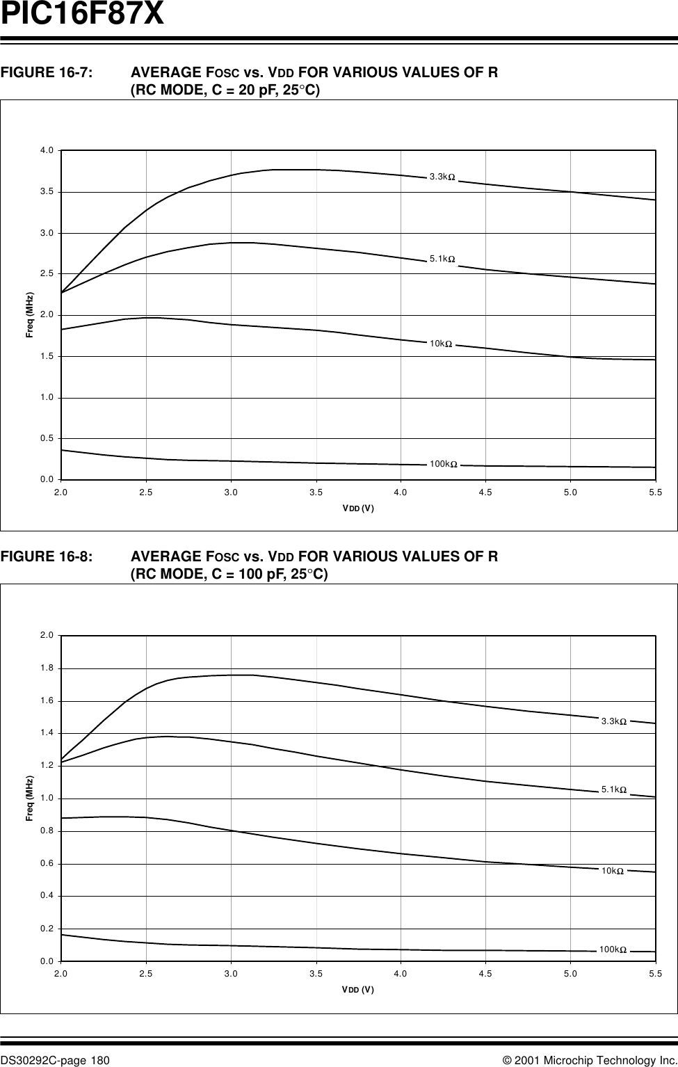
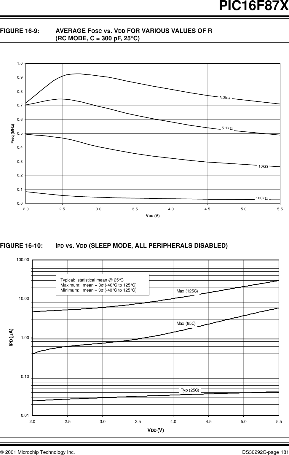
 2001 Microchip Technology Inc. DS30292C-page 157PIC16F87X15.3 DC Characteristics:  PIC16F873/874/876/877-04 (Extended)PIC16F873/874/876/877-10 (Extended) PIC16F873/874/876/877-04PIC16F873/874/876/877-20   (Extended)Standard Operating Conditions (unless otherwise stated)Operating temperature -40°C≤ TA ≤ +125°C Param No. Symbol Characteristic/Device Min Typ†Max Units ConditionsVDD Supply VoltageD001 4.0 —5.5 V LP, XT, RC osc configurationD001A 4.5 5.5 V HS osc configurationD001A VBOR 5.5 V BOR enabled, FMAX = 10 MHz(7)D002 VDR RAM Data Retention Voltage(1) —1.5 —VD003 VPOR VDD Start Voltage to ensure internal Power-on Reset signal—VSS —V See section on Power-on Reset for detailsD004 SVDD VDD Rise Rate to ensure internal Power-on Reset signal0.05 ——V/ms See section on Power-on Reset for detailsD005 VBOR Brown-out ResetVoltage 3.7 4.0 4.35 V BODEN bit in configuration word enabled† Data is “Typ” column is at 5V, 25°C, unless otherwise stated. These parameters are for design guidance only, and are not tested.Note 1: This is the limit to which VDD can be lowered without losing RAM data.2: The supply current is mainly a function of the operating voltage and frequency. Other factors such as I/O pin loading, switching rate, oscillator type, internal code execution pattern and temperature also have an impact on the current consumption.The test conditions for all IDD measurements in active operation mode are: OSC1 = external square wave, from rail to rail; all I/O pins tri-stated, pulled to VDD; MCLR = VDD; WDT enabled/disabled as specified. 3: The power-down current in SLEEP mode does not depend on the oscillator type. Power-down current is measured with the part in SLEEP mode, with all I/O pins in hi-impedance state and tied to VDD and VSS. 4: For RC osc configuration, current through REXT is not included. The current through the resistor can be estimated by the formula Ir = VDD/2REXT (mA) with REXT in kOhm.5: Timer1 oscillator (when enabled) adds approximately 20 µA to the specification. This value is from characterization and is for design guidance only. This is not tested.6: The ∆ current is the additional current consumed when this peripheral is enabled. This current should be added to the base IDD or IPD measurement.7: When BOR is enabled, the device will operate correctly until the VBOR voltage trip point is reached.
PIC16F87XDS30292C-page 158  2001 Microchip Technology Inc.IDD Supply Current(2,5)D010 —1.6 4 mA RC osc configurationsFOSC = 4 MHz, VDD = 5.5VD013 —7 15 mA HS osc configuration,FOSC = 10 MHz, VDD = 5.5VD015 ∆IBOR Brown-out Reset Current(6) —85 200 µA BOR enabled, VDD = 5.0VIPD Power-down Current(3,5)D020A 10.5 60 µAVDD = 4.0V, WDT enabledD021B 1.5 30 µAVDD = 4.0V, WDT disabledD023 ∆IBOR Brown-out Reset Current(6) —85 200 µA BOR enabled, VDD = 5.0V15.3 DC Characteristics:  PIC16F873/874/876/877-04 (Extended)PIC16F873/874/876/877-10 (Extended) (Continued)PIC16F873/874/876/877-04PIC16F873/874/876/877-20   (Extended)Standard Operating Conditions (unless otherwise stated)Operating temperature -40°C≤ TA ≤ +125°C Param No. Symbol Characteristic/Device Min Typ†Max Units Conditions† Data is “Typ” column is at 5V, 25°C, unless otherwise stated. These parameters are for design guidance only, and are not tested.Note 1: This is the limit to which VDD can be lowered without losing RAM data.2: The supply current is mainly a function of the operating voltage and frequency. Other factors such as I/O pin loading, switching rate, oscillator type, internal code execution pattern and temperature also have an impact on the current consumption.The test conditions for all IDD measurements in active operation mode are: OSC1 = external square wave, from rail to rail; all I/O pins tri-stated, pulled to VDD; MCLR = VDD; WDT enabled/disabled as specified. 3: The power-down current in SLEEP mode does not depend on the oscillator type. Power-down current is measured with the part in SLEEP mode, with all I/O pins in hi-impedance state and tied to VDD and VSS. 4: For RC osc configuration, current through REXT is not included. The current through the resistor can be estimated by the formula Ir = VDD/2REXT (mA) with REXT in kOhm.5: Timer1 oscillator (when enabled) adds approximately 20 µA to the specification. This value is from characterization and is for design guidance only. This is not tested.6: The ∆ current is the additional current consumed when this peripheral is enabled. This current should be added to the base IDD or IPD measurement.7: When BOR is enabled, the device will operate correctly until the VBOR voltage trip point is reached.
 2001 Microchip Technology Inc. DS30292C-page 159PIC16F87X15.4 DC Characteristics:  PIC16F873/874/876/877-04  (Extended)PIC16F873/874/876/877-10  (Extended) DC CHARACTERISTICSStandard Operating Conditions (unless otherwise stated)Operating temperature -40°C≤ TA ≤ +125°COperating voltage VDD range as described in DC specification (Section 15.1)ParamNo. Sym Characteristic Min Typ†Max Units ConditionsVIL Input Low VoltageI/O portsD030 with TTL buffer Vss —0.15VDD V For entire VDD rangeD030A Vss —0.8V V 4.5V ≤ VDD ≤ 5.5VD031 with Schmitt Trigger buffer Vss —0.2VDD VD032 MCLR, OSC1 (in RC mode) VSS —0.2VDD VD033 OSC1 (in XT, HS and LP) VSS —0.3VDD V(Note 1)Ports RC3 and RC4D034 with Schmitt Trigger buffer Vss —0.3VDD V For entire VDD rangeD034A with SMBus  -0.5 —0.6 V for VDD = 4.5 to 5.5VVIH Input High VoltageI/O ports —D040 with TTL buffer 2.0 —VDD V4.5V ≤ VDD ≤ 5.5VD040A 0.25VDD + 0.8V —VDD V For entire VDD rangeD041 with Schmitt Trigger buffer 0.8VDD —VDD V For entire VDD rangeD042 MCLR 0.8VDD —VDD VD042A OSC1 (XT, HS and LP) 0.7VDD —VDD V(Note 1)D043 OSC1 (in RC mode) 0.9VDD —VDD VPorts RC3 and RC4D044 with Schmitt Trigger buffer 0.7VDD —VDD V For entire VDD rangeD044A with SMBus 1.4 —5.5 V for VDD = 4.5 to 5.5VD070A IPURB PORTB Weak Pull-up Current 50 250 400 µAVDD = 5V, VPIN = VSS, IIL Input Leakage Current(2, 3)D060 I/O ports - - ±1µAVss ≤ VPIN ≤ VDD, Pin at hi-impedanceD061 MCLR, RA4/T0CKI - - ±5µAVss ≤ VPIN ≤ VDDD063 OSC1 - - ±5µAVss ≤ VPIN ≤ VDD, XT, HS and LP osc configuration* These parameters are characterized but not tested.†Data in "Typ" column is at 5V, 25°C unless otherwise stated. These parameters are for design guidanceonly and are not tested.Note 1: In RC oscillator configuration, the OSC1/CLKIN pin is a Schmitt Trigger input. It is not recommended that the PIC16F87X be driven with external clock in RC mode.2: The leakage current on the MCLR pin is strongly dependent on the applied voltage level. The specified levels represent normal operating conditions. Higher leakage current may be measured at different input voltages.3: Negative current is defined as current sourced by the pin.
PIC16F87XDS30292C-page 160  2001 Microchip Technology Inc.VOL Output Low VoltageD080A I/O ports ——0.6 V IOL = 7.0 mA, VDD = 4.5VD083A OSC2/CLKOUT (RC osc config) ——0.6 V IOL = 1.2 mA, VDD = 4.5VVOH Output High VoltageD090A I/O ports(3) VDD - 0.7 —— VIOH = -2.5 mA, VDD = 4.5VD092A OSC2/CLKOUT (RC osc config) VDD - 0.7 —— VIOH = -1.0 mA, VDD = 4.5VD150* VOD Open Drain High Voltage ——8.5 V RA4 pinCapacitive Loading Specs on Output PinsD100 COSC2 OSC2 pin ——15 pF In XT, HS and LP modes when external clock is used to drive OSC1D101D102 CIOCBAll I/O pins and OSC2 (RC mode) SCL, SDA (I2C mode) ————50400 pFpFData EEPROM MemoryD120 EDEndurance 100K ——E/W 25°C at 5VD121 VDRW VDD for read/write VMIN —5.5 V Using EECON to read/writeVMIN = min. operating voltageD122 TDEW Erase/write cycle time —48msProgram FLASH MemoryD130 EPEndurance 1000 ——E/W 25°C at 5VD131 VPR VDD for read VMIN —5.5 V VMIN = min operating voltageD132A VDD for erase/write VMIN —5.5 V Using EECON to read/write, VMIN = min. operating voltageD133 TPEW Erase/Write cycle time —48ms15.4 DC Characteristics:  PIC16F873/874/876/877-04  (Extended)PIC16F873/874/876/877-10  (Extended) (Continued)DC CHARACTERISTICSStandard Operating Conditions (unless otherwise stated)Operating temperature -40°C≤ TA ≤ +125°COperating voltage VDD range as described in DC specification (Section 15.1)ParamNo. Sym Characteristic Min Typ†Max Units Conditions* These parameters are characterized but not tested.†Data in "Typ" column is at 5V, 25°C unless otherwise stated. These parameters are for design guidanceonly and are not tested.Note 1: In RC oscillator configuration, the OSC1/CLKIN pin is a Schmitt Trigger input. It is not recommended that the PIC16F87X be driven with external clock in RC mode.2: The leakage current on the MCLR pin is strongly dependent on the applied voltage level. The specified levels represent normal operating conditions. Higher leakage current may be measured at different input voltages.3: Negative current is defined as current sourced by the pin.
 2001 Microchip Technology Inc. DS30292C-page 161PIC16F87X15.5 Timing Parameter SymbologyThe timing parameter symbols have been created fol-lowing one of the following formats:FIGURE 15-5: LOAD CONDITIONS1. TppS2ppS 3. TCC:ST (I2C specifications only)2. TppS 4. Ts  (I2C specifications only)TF Frequency T TimeLowercase letters (pp) and their meanings:ppcc CCP1 osc OSC1ck CLKOUT rd RDcs CS rw RD or WRdi SDI sc SCKdo SDO ss SSdt Data in t0 T0CKIio I/O port t1 T1CKImc MCLR wr WRUppercase letters and their meanings:SFFall PPeriodHHigh RRiseI Invalid (Hi-impedance) V ValidL Low Z Hi-impedanceI2C onlyAA output access High HighBUF Bus free Low LowTCC:ST (I2C specifications only)CCHD Hold SU SetupSTDAT DATA input hold STO STOP conditionSTA START conditionVDD/2CLRLPin PinVSS VSSCLRL= 464 ΩCL= 50 pF for all pins except OSC2, but including PORTD and PORTE outputs as ports,15 pF for OSC2 outputNote: PORTD and PORTE are not implemented on PIC16F873/876 devices.Load Condition 1 Load Condition 2
PIC16F87XDS30292C-page 162  2001 Microchip Technology Inc.FIGURE 15-6: EXTERNAL CLOCK TIMINGOSC1CLKOUTQ4 Q1 Q2 Q3 Q4 Q1123344TABLE 15-1: EXTERNAL CLOCK TIMING REQUIREMENTS Parameter No. Sym Characteristic Min Typ†Max Units ConditionsFOSC External CLKIN Frequency (Note 1) DC —4 MHz XT and RC osc modeDC —4 MHz HS osc mode (-04)DC —10 MHz HS osc mode (-10)DC —20 MHz HS osc mode (-20)DC —200 kHz LP osc mode Oscillator Frequency (Note 1) DC —4 MHz RC osc mode 0.1 —4MHzXT osc mode 4—10 MHz HS osc mode (-10)45——20200 MHzkHz HS osc mode (-20) LP osc mode1TOSC External CLKIN Period(Note 1) 250 ——ns XT and RC osc mode250 ——ns HS osc mode (-04)100 ——ns HS osc mode (-10)50 ——ns HS osc mode (-20)5——µs LP osc mode Oscillator Period(Note 1) 250 ——ns RC osc mode 250 —10,000 ns XT osc mode 250 ——ns HS osc mode (-04)100 —250 ns HS osc mode (-10)50 —250 ns HS osc mode (-20)5——µs LP osc mode2TCY Instruction Cycle Time (Note 1) 200 TCY DC ns TCY = 4/FOSC                             3 TosL,TosH External Clock in (OSC1) High or Low Time 100  ——ns XT oscillator2.5 ——µs LP oscillator15 ——ns HS oscillator4TosR,TosF External Clock in (OSC1) Rise or Fall Time — —25 ns XT oscillator— —50 ns LP oscillator—— 15 ns HS oscillator†Data in "Typ" column is at 5V, 25°C unless otherwise stated. These parameters are for design guidanceonly and are not tested.Note 1: Instruction cycle period (TCY) equals four times the input oscillator time-base period. All specified values are based on characterization data for that particular oscillator type under standard operating conditions, with the device executing code. Exceeding these specified limits may result in an unstable oscillator operation and/or higher than expected current consumption. All devices are tested to operate at "min." values with an external clock applied to the OSC1/CLKIN pin. When an external clock input is used, the "max." cycle time limit is "DC" (no clock) for all devices.
 2001 Microchip Technology Inc. DS30292C-page 163PIC16F87XFIGURE 15-7: CLKOUT AND I/O TIMINGTABLE 15-2: CLKOUT AND I/O TIMING REQUIREMENTSNote: Refer to Figure 15-5 for load conditions.OSC1CLKOUTI/O Pin(Input)I/O Pin(Output)Q4 Q1 Q2 Q31013 141720, 2119 18151112 16Old Value New ValueParamNo. Symbol Characteristic Min Typ†Max Units Conditions10* TosH2ckL OSC1↑ to CLKOUT↓ —75 200 ns (Note 1)11* TosH2ckHOSC1↑ to CLKOUT↑ —75 200 ns (Note 1)12* TckR CLKOUT rise time  —35 100 ns (Note 1)13* TckF CLKOUT fall time  —35 100 ns (Note 1)14* TckL2ioV CLKOUT ↓ to Port out valid  ——0.5TCY + 20 ns (Note 1)15* TioV2ckH Port in valid before CLKOUT ↑ TOSC + 200 ——ns  (Note 1)16* TckH2ioI Port in hold after CLKOUT ↑ 0——ns (Note 1)17* TosH2ioV OSC1↑ (Q1 cycle) to Port out valid—100 255 ns18* TosH2ioI OSC1↑ (Q2 cycle) to Port input invalid (I/O in hold time)Standard (F) 100 ——nsExtended (LF) 200 ——ns19* TioV2osH Port input valid to OSC1↑ (I/O in setup time) 0 ——ns20* TioR Port output rise time  Standard (F)—10 40 nsExtended (LF)——145 ns21* TioF Port output fall time Standard (F)—10 40 nsExtended (LF)——145 ns22††* Tinp INT pin high or low time TCY ——ns23††* Trbp RB7:RB4 change INT high or low time TCY ——ns*  These parameters are characterized but not tested.†Data in "Typ" column is at 5V, 25°C unless otherwise stated. These parameters are for design guidance only and are not tested.††  These parameters are asynchronous events not related to any internal clock edges.Note 1:  Measurements are taken in RC mode where CLKOUT output is 4 x TOSC.
PIC16F87XDS30292C-page 164  2001 Microchip Technology Inc.FIGURE 15-8: RESET, WATCHDOG TIMER, OSCILLATOR START-UP TIMER AND POWER-UP TIMER TIMINGFIGURE 15-9: BROWN-OUT RESET TIMINGTABLE 15-3: RESET, WATCHDOG TIMER, OSCILLATOR START-UP TIMER, POWER-UP TIMER, AND BROWN-OUT RESET REQUIREMENTSVDDMCLRInternalPORPWRTTime-outOSCTime-outInternalResetWatchdogTimerReset3332303134I/O Pins34Note: Refer to Figure 15-5 for load conditions.VDD VBOR35Parameter No. Symbol Characteristic Min Typ†Max Units Conditions30 TmcL MCLR Pulse Width (low)                2  ——µsVDD = 5V, -40°C to +85°C31* Twdt Watchdog Timer Time-out Period (No Prescaler)71833msVDD = 5V, -40°C to +85°C32 Tost Oscillation Start-up Timer Period —1024 TOSC ——TOSC = OSC1 period33* Tpwrt Power-up Timer Period 28 72 132 ms  VDD = 5V, -40°C to +85°C34 TIOZ  I/O Hi-impedance from MCLR Low or Watchdog Timer Reset——2.1 µs35 TBOR Brown-out Reset pulse width 100 ——µsVDD ≤ VBOR (D005)* These parameters are characterized but not tested.†Data in "Typ" column is at 5V, 25°C unless otherwise stated. These parameters are for design guidance only and are not tested.
 2001 Microchip Technology Inc. DS30292C-page 165PIC16F87XFIGURE 15-10: TIMER0 AND TIMER1 EXTERNAL CLOCK TIMINGSTABLE 15-4: TIMER0 AND TIMER1 EXTERNAL CLOCK REQUIREMENTS Param No. Symbol Characteristic Min Typ†Max Units Conditions40* Tt0H T0CKI High Pulse Width No Prescaler 0.5TCY + 20 ——ns Must also meet parameter 42 With Prescaler 10 ——ns41* Tt0L T0CKI Low Pulse Width No Prescaler 0.5TCY + 20 ——ns Must also meet parameter 42 With Prescaler 10 ——ns42* Tt0P T0CKI Period No Prescaler TCY + 40 ——nsWith Prescaler Greater of:20 or TCY + 40         N——ns N = prescale value (2, 4,..., 256)45* Tt1H T1CKI High Time Synchronous, Prescaler = 1 0.5TCY + 20 ——ns Must also meet parameter 47 Synchronous, Prescaler = 2,4,8Standard(F)15——nsExtended(LF)25——nsAsynchronous Standard(F)30——nsExtended(LF)50——ns46* Tt1L T1CKI Low Time Synchronous, Prescaler = 1 0.5TCY + 20 ——ns Must also meet parameter 47 Synchronous, Prescaler = 2,4,8Standard(F)15——nsExtended(LF)25——nsAsynchronous Standard(F)30——nsExtended(LF)50——ns47* Tt1P T1CKI input period Synchronous Standard(F) Greater of:30 OR TCY + 40           N——ns N = prescale value (1, 2, 4, 8)Extended(LF) Greater of:50 OR TCY + 40        NN = prescale value (1, 2, 4, 8)Asynchronous Standard(F)60——nsExtended(LF) 100 ——nsFt1 Timer1 oscillator input frequency range (oscillator enabled by setting bit T1OSCEN)DC — 200 kHz48 TCKEZtmr1 Delay from external clock edge to timer increment 2TOSC —7TOSC —*  These parameters are characterized but not tested.†Data in "Typ" column is at 5V, 25°C unless otherwise stated. These parameters are for design guidance only and are not tested.Note: Refer to Figure 15-5 for load conditions.46474548414240RA4/T0CKIRC0/T1OSO/T1CKITMR0 orTMR1
PIC16F87XDS30292C-page 166  2001 Microchip Technology Inc.FIGURE 15-11: CAPTURE/COMPARE/PWM TIMINGS (CCP1 AND CCP2)TABLE 15-5: CAPTURE/COMPARE/PWM REQUIREMENTS (CCP1 AND CCP2)Note: Refer to Figure 15-5 for load conditions. and RC2/CCP1(Capture Mode)50 515253 54RC1/T1OSI/CCP2 and RC2/CCP1(Compare or PWM Mode)RC1/T1OSI/CCP2Param No. Sym Characteristic Min Typ†Max Units Conditions50* TccL CCP1 and CCP2input low timeNo Prescaler 0.5TCY + 20 ——nsWith PrescalerStandard(F)10——nsExtended(LF)20——ns51* TccH CCP1 and CCP2input high timeNo Prescaler 0.5TCY + 20 ——nsWith PrescalerStandard(F)10——nsExtended(LF)20——ns52* TccP CCP1 and CCP2 input period 3TCY + 40N——ns N = prescale value (1, 4 or 16)53* TccR CCP1 and CCP2 output rise time Standard(F)—10 25 nsExtended(LF)—25 50 ns54* TccF CCP1 and CCP2 output fall time Standard(F)—10 25 nsExtended(LF)—25 45 ns*  These parameters are characterized but not tested.†Data in "Typ" column is at 5V, 25°C unless otherwise stated. These parameters are for design guidance only and are not tested.
 2001 Microchip Technology Inc. DS30292C-page 167PIC16F87XFIGURE 15-12: PARALLEL SLAVE PORT TIMING (PIC16F874/877 ONLY)TABLE 15-6: PARALLEL SLAVE PORT REQUIREMENTS (PIC16F874/877 ONLY)Note: Refer to Figure 15-5 for load conditions.RE2/CSRE0/RDRE1/WRRD7:RD062636465Parameter No. Symbol Characteristic Min Typ†Max Units Conditions62 TdtV2wrH Data in valid before WR↑ or CS↑ (setup time) 2025————nsns Extended Range Only63* TwrH2dtI WR↑ or CS↑ to data–in invalid (hold time)  Standard(F)20——ns  Extended(LF)35——ns64 TrdL2dtV RD↓ and CS↓ to data–out valid ————8090nsns Extended Range Only65 TrdH2dtI RD↑ or CS↓ to data–out invalid 10 —30 ns* These parameters are characterized but not tested.†Data in "Typ" column is at 5V, 25°C unless otherwise stated. These parameters are for design guidance only and are not tested.
PIC16F87XDS30292C-page 168  2001 Microchip Technology Inc.FIGURE 15-13: SPI MASTER MODE TIMING (CKE = 0, SMP = 0)FIGURE 15-14: SPI MASTER MODE TIMING (CKE = 1, SMP = 1)SSSCK(CKP = 0)SCK(CKP = 1)SDOSDI7071 72737475, 767879807978MSb LSbBIT6 - - - - - -1MSb IN LSb INBIT6 - - - -1Note: Refer to Figure 15-5 for load conditions.SSSCK(CKP = 0)SCK(CKP = 1)SDOSDI8171 727475, 767880MSb7973MSb INBIT6 - - - - - -1LSb INBIT6 - - - -1LSbNote: Refer to Figure 15-5 for load conditions.
 2001 Microchip Technology Inc. DS30292C-page 169PIC16F87XFIGURE 15-15: SPI SLAVE MODE TIMING (CKE = 0)FIGURE 15-16: SPI SLAVE MODE TIMING (CKE = 1)SSSCK(CKP = 0)SCK(CKP = 1)SDOSDI7071 72737475, 76 777879807978SDIMSb LSbBIT6 - - - - - -1MSb IN BIT6 - - - -1 LSb IN83Note: Refer to Figure 15-5 for load conditions.SSSCK(CKP = 0)SCK(CKP = 1)SDOSDI7071 7282SDI7475, 76MSb BIT6 - - - - - -1 LSb77MSb IN BIT6 - - - -1 LSb IN8083Note: Refer to Figure 15-5 for load conditions.
PIC16F87XDS30292C-page 170  2001 Microchip Technology Inc.TABLE 15-7: SPI MODE REQUIREMENTS   FIGURE 15-17: I2C BUS START/STOP BITS TIMINGParam No. Symbol Characteristic Min Typ†Max Units Conditions70* TssL2scH, TssL2scLSS↓ to SCK↓ or SCK↑ input Tcy ——ns71* TscH SCK input high time (Slave mode) TCY + 20 ——ns72* TscL SCK input low time (Slave mode) TCY + 20 ——ns73* TdiV2scH, TdiV2scLSetup time of SDI data input to SCK edge 100 ——ns74* TscH2diL, TscL2diLHold time of SDI data input to SCK edge 100 ——ns75* TdoR SDO data output rise time Standard(F)Extended(LF)——10252550nsns76* TdoF SDO data output fall time —10 25 ns77* TssH2doZ SS↑ to SDO output hi-impedance  10 —50 ns78* TscR SCK output rise time (Master mode) Standard(F)Extended(LF)——10252550nsns79* TscF SCK output fall time (Master mode) —10 25 ns80* TscH2doV,TscL2doVSDO data output valid after SCK edgeStandard(F)Extended(LF)————50145ns81* TdoV2scH,TdoV2scLSDO data output setup to SCK edge Tcy ——ns82* TssL2doV SDO data output valid after SS↓ edge ——50 ns83* TscH2ssH,TscL2ssHSS ↑ after SCK edge 1.5TCY + 40 ——ns* These parameters are characterized but not tested.†Data in "Typ" column is at 5V, 25°C unless otherwise stated. These parameters are for design guidance only and are not tested.Note: Refer to Figure 15-5 for load conditions.91 93SCLSDASTARTCondition STOPCondition90 92
 2001 Microchip Technology Inc. DS30292C-page 171PIC16F87XTABLE 15-8: I2C BUS START/STOP BITS REQUIREMENTSFIGURE 15-18: I2C BUS DATA TIMINGParameterNo. Symbol Characteristic Min Typ Max Units Conditions90 Tsu:sta START condition  100 kHz mode 4700 —— ns Only relevant for Repeated START conditionSetup time 400 kHz mode 600 ——91 Thd:sta START condition  100 kHz mode 4000 —— ns After this period, the first clock pulse is generatedHold time 400 kHz mode 600 ——92 Tsu:sto STOP condition 100 kHz mode 4700 —— nsSetup time 400 kHz mode 600 ——93 Thd:sto STOP condition 100 kHz mode  4000 —— nsHold time 400 kHz mode 600 ——Note: Refer to Figure 15-5 for load conditions.9091 92100101103106 107109 109 110102SCLSDAInSDAOut
PIC16F87XDS30292C-page 172  2001 Microchip Technology Inc.TABLE 15-9: I2C BUS DATA REQUIREMENTSParamNo. Sym Characteristic Min Max Units Conditions100 Thigh Clock high time    100 kHz mode 4.0 —µs Device must operate at a minimum of 1.5 MHz400 kHz mode 0.6 —µs Device must operate at a minimum of 10 MHzSSP Module 0.5TCY —101 Tlow Clock low time 100 kHz mode 4.7 —µs Device must operate at a minimum of 1.5 MHz400 kHz mode 1.3 —µs Device must operate at a minimum of 10 MHzSSP Module 0.5TCY —102 Tr SDA and SCL rise time100 kHz mode  —1000 ns400 kHz mode 20 + 0.1Cb 300 ns Cb is specified to be from 10 to 400 pF 103 Tf SDA and SCL fall time 100 kHz mode  —300 ns400 kHz mode 20 + 0.1Cb 300 ns Cb is specified to be from 10 to 400 pF 90 Tsu:sta START condition setup time100 kHz mode 4.7 —µs Only relevant for Repeated START condition400 kHz mode 0.6 —µs91 Thd:sta START condition hold time 100 kHz mode 4.0 —µs After this period, the first clock pulse is generated400 kHz mode 0.6 —µs106 Thd:dat Data input hold time 100 kHz mode  0 —ns400 kHz mode 0 0.9 µs107 Tsu:dat Data input setup time 100 kHz mode 250 —ns (Note 2)400 kHz mode 100 —ns92 Tsu:sto STOP condition setup time100 kHz mode 4.7 —µs400 kHz mode 0.6 —µs109 Taa Output valid from clock100 kHz mode —3500 ns (Note 1)400 kHz mode ——ns110 Tbuf Bus free time 100 kHz mode 4.7 —µs Time the bus must be free before a new transmission can start400 kHz mode 1.3 —µsCb Bus capacitive loading — 400 pF Note 1: As a transmitter, the device must provide this internal minimum delay time to bridge the undefined region (min. 300 ns) of the falling edge of SCL to avoid unintended generation of START or STOP conditions.2: A fast mode (400 kHz) I2C bus device can be used in a standard mode (100 kHz) I2C bus system, but the requirement that Tsu:dat ≥250 ns must then be met. This will automatically be the case if the device does not stretch the LOW period of the SCL signal. If such a device does stretch the LOW period of the SCL signal, it must output the next data bit to the SDA line TR max.+ Tsu:dat = 1000 + 250 = 1250 ns (according to the standard mode I2C bus specification) before the SCL line is released.
 2001 Microchip Technology Inc. DS30292C-page 173PIC16F87XFIGURE 15-19: USART SYNCHRONOUS TRANSMISSION (MASTER/SLAVE) TIMINGTABLE 15-10: USART SYNCHRONOUS TRANSMISSION REQUIREMENTSFIGURE 15-20: USART SYNCHRONOUS RECEIVE (MASTER/SLAVE) TIMINGTABLE 15-11: USART SYNCHRONOUS RECEIVE REQUIREMENTSNote: Refer to Figure 15-5 for load conditions.121121122RC6/TX/CKRC7/RX/DTPinPin120ParamNo. Sym Characteristic Min Typ†Max Units Conditions120 TckH2dtV SYNC XMIT (MASTER & SLAVE)Clock high to data out validStandard(F)——80 nsExtended(LF)——100 ns121 Tckrf Clock out rise time and fall time (Master mode)Standard(F)——45 nsExtended(LF)——50 ns122 Tdtrf Data out rise time and fall time Standard(F)——45 nsExtended(LF)——50 ns†Data in “Typ” column is at 5V, 25°C unless otherwise stated. These parameters are for design guidance only and are not tested.Note: Refer to Figure 15-5 for load conditions.125126RC6/TX/CKRC7/RX/DTpinpinParameter No. Sym Characteristic Min Typ†Max Units Conditions125 TdtV2ckL SYNC RCV (MASTER & SLAVE)Data setup before CK ↓ (DT setup time) 15 —— ns126 TckL2dtl Data hold after CK ↓ (DT hold time) 15 —— ns†Data in “Typ” column is at 5V, 25°C unless otherwise stated. These parameters are for design guidance only and are not tested.
PIC16F87XDS30292C-page 174  2001 Microchip Technology Inc.TABLE 15-12: PIC16F87X-04 (COMMERCIAL, INDUSTRIAL, EXTENDED)PIC16F87X-10 (EXTENDED)PIC16F87X-20 (COMMERCIAL, INDUSTRIAL)PIC16LF87X-04 (COMMERCIAL, INDUSTRIAL)     ParamNo. Sym Characteristic Min Typ†Max Units ConditionsA01 NRResolution ——10-bits bit VREF = VDD = 5.12V, VSS ≤ VAIN ≤ VREFA03 EIL Integral linearity error ——< ± 1 LSb VREF = VDD = 5.12V, VSS ≤ VAIN ≤ VREFA04 EDL Differential linearity error ——< ± 1 LSb VREF = VDD = 5.12V, VSS ≤ VAIN ≤ VREFA06 EOFF Offset error ——< ± 2 LSb VREF = VDD = 5.12V, VSS ≤ VAIN ≤ VREFA07 EGN Gain error ——< ± 1 LSb VREF = VDD = 5.12V, VSS ≤ VAIN ≤ VREFA10 —Monotonicity(3) —guaranteed ——VSS ≤ VAIN ≤ VREFA20 VREF Reference voltage (VREF+ - VREF-)  2.0 —VDD + 0.3 V Absolute minimum electrical spec. To ensure 10-bit accuracy.A21 VREF+ Reference voltage High AVDD - 2.5V AVDD + 0.3V VA22 VREF- Reference voltage low AVSS - 0.3V VREF+ - 2.0V VA25 VAIN Analog input voltage VSS - 0.3 V —VREF + 0.3 V  VA30 ZAIN Recommended impedance of analog voltage source——10.0 kΩA40 IAD A/D conversion current (VDD)Standard —220 —µA Average current consumption when A/D is on (Note 1)Extended —90 —µAA50 IREF VREF input current (Note 2) 10———100010µAµADuring VAIN acquisition.Based on differential of VHOLD to VAIN to charge CHOLD, see Section 11.1.During A/D Conversion cycle* These parameters are characterized but not tested.†Data in "Typ" column is at 5V, 25°C unless otherwise stated. These parameters are for design guidance only and are not tested.Note 1: When A/D is off, it will not consume any current other than minor leakage current. The power-down current spec includes any such leakage from the A/D module.2: VREF current is from RA3 pin or VDD pin, whichever is selected as reference input.3: The A/D conversion result never decreases with an increase in the input voltage, and has no missing codes.
 2001 Microchip Technology Inc. DS30292C-page 175PIC16F87XFIGURE 15-21: A/D CONVERSION TIMINGTABLE 15-13: A/D CONVERSION REQUIREMENTS131130132BSF ADCON0, GOQ4A/D CLKA/D DATAADRESADIFGOSAMPLEOLD_DATASAMPLING STOPPEDDONENEW_DATA(TOSC/2)(1)987 210Note: If the A/D clock source is selected as RC, a time of TCY is added before the A/D clock starts. This allows the SLEEPinstruction to be executed. 1 TCY. . . . . .Param No. Sym Characteristic Min Typ†Max Units Conditions130 TAD A/D clock period Standard(F)1.6——µsTOSC based, VREF ≥ 3.0VExtended(LF)3.0——µsTOSC based, VREF ≥ 2.0VStandard(F) 2.0 4.0 6.0 µs A/D RC modeExtended(LF) 3.0 6.0 9.0 µs A/D RC mode131 TCNV Conversion time (not including S/H time) (Note 1) —12 TAD132 TACQ Acquisition time   (Note 2)10*40———µsµs The minimum time is the amplifier settling time. This may be used if the "new" input volt-age has not changed by more than 1 LSb (i.e., 20.0 mV @ 5.12V) from the last sampled voltage (as stated on CHOLD).134 TGO Q4 to A/D clock start —TOSC/2 §— —If the A/D clock source is selected as RC, a time of TCY is added before the A/D clock starts. This allows the SLEEP instruction to be executed.* These parameters are characterized but not tested.†Data in "Typ" column is at 5V, 25°C unless otherwise stated. These parameters are for design guidance only and are not tested.§This specification ensured by design.Note 1: ADRES register may be read on the following TCY cycle.2: See Section 11.1 for minimum conditions.
PIC16F87XDS30292C-page 176  2001 Microchip Technology Inc.NOTES:
 2001 Microchip Technology Inc. DS30292C-page 177PIC16F87X16.0 DC AND AC CHARACTERISTICS GRAPHS AND TABLESThe graphs and tables provided in this section are for design guidance and are not tested. In some graphs or tables, the data presented is outside specified operating range (i.e., outside specified VDD range).This is for information only and devices are ensured to operate properly only within the specified range.The data presented in this section is a statistical summary of data collected on units from different lots over a periodof time and matrix samples. ’Typical’ represents the mean of the distribution at 25°C.  ’max’ or ’min’ represents(mean + 3σ) or (mean - 3σ) respectively, where σ is standard deviation, over the whole temperature range.FIGURE 16-1: TYPICAL IDD vs. FOSC OVER VDD (HS MODE) FIGURE 16-2: MAXIMUM IDD vs. FOSC OVER VDD (HS MODE) 012345674 6 8 101214161820FOSC (M Hz )IDD (mA)2.5V2.0V5.5V5.0V4.5V4.0V3.5V3.0VTypical:  statistical mean @ 25°CMaximum:  mean + 3s (-40°C to 125°C) Minimum:   mean – 3s (-40°C to 125°C)0123456784 6 8 101214161820FOSC (M Hz)IDD (mA)5.5V5.0V4.5V4.0V3.5V3.0V2.5V2.0VTypical:  statistical mean @ 25°CMaximum:  mean + 3s (-40°C to 125°C) Minimum:   mean – 3s (-40°C to 125°C)
PIC16F87XDS30292C-page 178 © 2001 Microchip Technology Inc.FIGURE 16-3: TYPICAL IDD vs. FOSC OVER VDD (XT MODE) FIGURE 16-4: MAXIMUM IDD vs. FOSC OVER VDD (LP MODE) 0.00.20.40.60.81.01.21.41.60.00.51.01.52.02.53.03.54.0FOSC (MHz)IDD (mA)5.5V5.0V4.5V4.0V3.5V2.5V2.0V3.0VTypical:  statistical mean @ 25°CMaximum:  mean + 3s (-40°C to 125°C) Minimum:   mean – 3s (-40°C to 125°C)0.00.20.40.60.81.01.21.41.61.82.00.0 0.5 1.0 1.5 2.0 2.5 3.0 3.5 4.0FOSC (MHz)IDD (mA)5.5V5.0V4.5V4.0V3.5V2.5V2.0V3.0VTypical:  statistical mean @ 25°CMaximum:  mean + 3s (-40°C to 125°C) Minimum:   mean – 3s (-40°C to 125°C)
 2001 Microchip Technology Inc. DS30292C-page 179PIC16F87XFIGURE 16-5: TYPICAL IDD vs. FOSC OVER VDD (LP MODE)FIGURE 16-6: MAXIMUM IDD vs. FOSC OVER VDD (XT MODE)010203040506070809020 30 40 50 60 70 80 90 100FOSC (kHz)IDD (uA)5.5V5.0V4.5V4.0V3.5V3.0V2.5V2.0VTypical:  statistical mean @ 25°CMaximum:  mean + 3s (-40°C to 125°C) Minimum:   mean – 3s (-40°C to 125°C)010203040506070809010011012020 30 40 50 60 70 80 90 100FOSC (kHz)IDD (uA)5.5V5.0V4.5V4.0V3.5V3.0V2.5V2.0VTypical:  statistical mean @ 25°CMaximum:  mean + 3s (-40°C to 125°C) Minimum:   mean – 3s (-40°C to 125°C)
PIC16F87XDS30292C-page 180 © 2001 Microchip Technology Inc.FIGURE 16-7: AVERAGE FOSC vs. VDD FOR VARIOUS VALUES OF R (RC MODE, C = 20 pF, 25°C)FIGURE 16-8: AVERAGE FOSC vs. VDD FOR VARIOUS VALUES OF R(RC MODE, C = 100 pF, 25°C)0.00.51.01.52.02.53.03.54.02.02.53.03.54.04.55.05.5VDD (V)Freq (MHz)3.3kΩ5.1kΩ10kΩ100kΩ0.00.20.40.60.81.01.21.41.61.82.02.02.53.03.54.04.55.05.5VDD (V)Freq (MHz)3.3kΩ5.1kΩ10kΩ100kΩ
 2001 Microchip Technology Inc. DS30292C-page 181PIC16F87XFIGURE 16-9: AVERAGE FOSC vs. VDD FOR VARIOUS VALUES OF R (RC MODE, C = 300 pF, 25°C)FIGURE 16-10: IPD vs. VDD (SLEEP MODE, ALL PERIPHERALS DISABLED)0.00.10.20.30.40.50.60.70.80.91.02.02.53.03.54.04.55.05.5VDD (V)Freq (MHz)3.3kΩ5.1kΩ10kΩ100kΩ0.010.101.0010.00100.002.0 2.5 3.0 3.5 4.0 4.5 5.0 5.5VDD (V)IPD (µA)Max (125C)Max (85C)Typ (25C)Typical:  statistical mean @ 25°CMaximum:  mean + 3σ (-40°C to 125°C) Minimum:   mean – 3σ (-40°C to 125°C)
PIC16F87XDS30292C-page 182 © 2001 Microchip Technology Inc.FIGURE 16-11: ∆IBOR vs. VDD OVER TEMPERATUREFIGURE 16-12: TYPICAL AND MAXIMUM ∆ITMR1 vs. VDD OVER TEMPERATURE (-10°C TO 70°C, TIMER1 WITH OSCILLATOR, XTAL=32 kHZ, C1 AND C2=50 pF)0.00.20.40.60.81.01.22.5 3.0 3.5 4.0 4.5 5.0 5.5VDD (V)∆IBOR (mA)Device in SleepDevice in ResetMax ResetTyp Reset (25C)Max SleepTyp Sleep (25C)IndeterminateStateTypical:  statistical mean @ 25°CMaximum:  mean + 3s (-40°C to 125°C) Minimum:   mean – 3s (-40°C to 125°C)Note: Device current in RESET depends on oscillator mode, frequency and circuit.01020304050607080902.0 2.5 3.0 3.5 4.0 4.5 5.0 5.5VDD (V)∆ITMR1 (uA)Typ (25C)Max  Typical:  statistical mean @ 25°CMaximum:  mean + 3s (-40°C to 125°C) Minimum:   mean – 3s (-40°C to 125°C)
 2001 Microchip Technology Inc. DS30292C-page 183PIC16F87XFIGURE 16-13: TYPICAL AND MAXIMUM ∆IWDT vs. VDD OVER TEMPERATUREFIGURE 16-14: TYPICAL, MINIMUM AND MAXIMUM WDT PERIOD vs. VDD (-40°C TO 125°C)024681012142.02.53.03.54.04.55.05.5VDD (V)∆IWDT (uA)Typ (25C)Max (85C)Typical:  statistical mean @ 25°CMaximum:  mean + 3s (-40°C to 125°C) Minimum:   mean – 3s (-40°C to 125°C)01020304050602.0 2.5 3.0 3.5 4.0 4.5 5.0 5.5VDD (V)WDT Period (ms)Min (-40C)Typ (25C)Max (125C)Typical:  statistical mean @ 25°CMaximum:  mean + 3s (-40°C to 125°C) Minimum:   mean – 3s (-40°C to 125°C)
PIC16F87XDS30292C-page 184 © 2001 Microchip Technology Inc.FIGURE 16-15: AVERAGE WDT PERIOD vs. VDD OVER TEMPERATURE (-40°C TO 125°C) FIGURE 16-16: TYPICAL, MINIMUM AND MAXIMUM VOH vs. IOH (VDD=5V, -40°C TO 125°C)051015202530354045502.0 2.5 3.0 3.5 4.0 4.5 5.0 5.5VDD (V)WDT Period (ms)85C125C25C-40CTypical:  statistical mean @ 25°CMaximum:  mean + 3s (-40°C to 125°C) Minimum:   mean – 3s (-40°C to 125°C)2.02.53.03.54.04.55.00 5 10 15 20 25IOH (-mA)VOH (V)Max (-40C)Typ (25C)Min (125C)Typical:  statistical mean @ 25°CMaximum:  mean + 3s (-40°C to 125°C) Minimum:   mean – 3s (-40°C to 125°C)
 2001 Microchip Technology Inc. DS30292C-page 185PIC16F87XFIGURE 16-17: TYPICAL, MINIMUM AND MAXIMUM VOH vs. IOH (VDD=3V, -40°C TO 125°C)FIGURE 16-18: TYPICAL, MINIMUM AND MAXIMUM VOL vs. IOL (VDD=5V, -40°C TO 125°C)0.00.51.01.52.02.53.00 5 10 15 20 25IOH (-mA)VOH (V)Max (-40C)Typ (25C)Min (125C)Typical:  statistical mean @ 25°CMaximum:  mean + 3s (-40°C to 125°C) Minimum:   mean – 3s (-40°C to 125°C)0.00.20.40.60.81.01.21.41.61.82.00 5 10 15 20 25IOL (-mA)VOL (V)Max (125C)Typ (25C)Min (-40C)Typical:  statistical mean @ 25°CMaximum:  mean + 3s (-40°C to 125°C) Minimum:   mean – 3s (-40°C to 125°C)
PIC16F87XDS30292C-page 186 © 2001 Microchip Technology Inc.FIGURE 16-19: TYPICAL, MINIMUM AND MAXIMUM VOL vs. IOL (VDD=3V, -40°C TO 125°C)FIGURE 16-20: MINIMUM AND MAXIMUM VIN vs. VDD, (TTL INPUT, -40°C TO 125°C) 0.00.51.01.52.02.53.00 5 10 15 20 25IOL (-mA)VOL (V)Max (125C)Typ (25C)Min (-40C)Typical:  statistical mean @ 25°CMaximum:  mean + 3s (-40°C to 125°C) Minimum:   mean – 3s (-40°C to 125°C)0.00.20.40.60.81.01.21.41.61.82.0 2.5 3.0 3.5 4.0 4.5 5.0 5.5VDD (V)VIN (V)Max (-40C)Min (125C)Typical:  statistical mean @ 25°CMaximum:  mean + 3s (-40°C to 125°C) Minimum:   mean – 3s (-40°C to 125°C)
 2001 Microchip Technology Inc. DS30292C-page 187PIC16F87XFIGURE 16-21: MINIMUM AND MAXIMUM VIN vs. VDD (ST INPUT, -40°C TO 125°C) FIGURE 16-22: MINIMUM AND MAXIMUM VIN vs. VDD (I2C INPUT, -40°C TO 125°C)0.00.51.01.52.02.53.03.54.04.52.02.53.03.54.04.55.05.5VDD (V)VIN (V)Max High (125C)Max Low (125C)Min High (-40C)Min Low (-40C)Typical:  statistical mean @ 25°CMaximum:  mean + 3s (-40°C to 125°C) Minimum:   mean – 3s (-40°C to 125°C)0.00.51.01.52.02.53.03.52.02.53.03.54.04.55.05.5VDD (V)VIN (V)Max High (125C)Max Low (125C)Min High (-40C)Min Low (25C)Typical:  statistical mean @ 25°CMaximum:  mean + 3s (-40°C to 125°C) Minimum:   mean – 3s (-40°C to 125°C)
PIC16F87XDS30292C-page 188 © 2001 Microchip Technology Inc.NOTES:
 2001 Microchip Technology Inc. DS30292C-page 189PIC16F87X17.0 PACKAGING INFORMATION17.1 Package Marking Information28-Lead SOICYYWWNNNExampleXXXXXXXXXXXXXXXXXYYWWNNN28-Lead PDIP (Skinny DIP) ExampleXXXXXXXXXXXXXXXXXXXXXXXXXXXXXXXXXXXXXXXXXXXXXXXXXXXXXXXXX0117HATPIC16F876-20/SPXXXXXXXXXXXXXXXXXXXX0110SAAPIC16F876-04/SOLegend:    XX...X Customer specific information*YY Year code (last 2 digits of calendar year)WW Week code (week of January 1 is week ‘01’)NNN Alphanumeric traceability codeNote: In the event the full Microchip part number cannot be marked on one line, it willbe carried over to the next line thus limiting the number of available charactersfor customer specific information.*Standard OTP marking consists of Microchip part number, year code, week code, facility code, maskrev#, and assembly code.  For  OTP marking beyond this, certain price adders apply.  Please check withyour Microchip Sales Office.  For QTP devices, any special marking adders are included in QTP price.
PIC16F87XDS30292C-page 190  2001 Microchip Technology Inc.Package Marking Information (Cont’d)XXXXXXXXXXXXXXXXXXYYWWNNN40-Lead PDIP Example44-Lead TQFPXXXXXXXXXXYYWWNNNXXXXXXXXXXExample44-Lead PLCC44-Lead MQFPExampleExampleXXXXXXXXXXXXXXXXXXXXXXXXXXXXXXXXXXXXXXXXXXXXXXXXXXXXXXXXYYWWNNNXXXXXXXXXXXXXXXXXXXXPIC16F877-04/P0112SAA-04/PT0111HATPIC16F877XXXXXXXXXXYYWWNNNXXXXXXXXXXXXXXXXXXXX -20/PQ0104SATPIC16F877-20/L0103SATPIC16F877
 2001 Microchip Technology Inc. DS30292C-page 191PIC16F87X28-Lead Skinny Plastic Dual In-line (SP) – 300 mil (PDIP) 1510515105βMold Draft Angle Bottom1510515105αMold Draft Angle Top10.928.898.13.430.350.320eBOverall Row Spacing §0.560.480.41.022.019.016BLower Lead Width1.651.331.02.065.053.040B1Upper Lead Width0.380.290.20.015.012.008cLead Thickness3.433.303.18.135.130.125LTip to Seating Plane35.1834.6734.161.3851.3651.345DOverall Length7.497.246.99.295.285.275E1Molded Package Width8.267.877.62.325.310.300EShoulder to Shoulder Width0.38.015A1Base to Seating Plane3.433.303.18.135.130.125A2Molded Package Thickness4.063.813.56.160.150.140ATop to Seating Plane2.54.100pPitch2828nNumber of PinsMAXNOMMINMAXNOMMINDimension LimitsMILLIMETERSINCHES*Units21DnE1ceBβEαpLA2BB1AA1Notes:JEDEC Equivalent:  MO-095Drawing No. C04-070* Controlling ParameterDimension D and E1 do not include mold flash or protrusions. Mold flash or protrusions shall not exceed .010” (0.254mm) per side. § Significant Characteristic
PIC16F87XDS30292C-page 192  2001 Microchip Technology Inc.28-Lead Plastic Small Outline (SO) –Wide, 300 mil (SOIC)Foot Angle Top φ0480481512015120βMold Draft Angle Bottom1512015120αMold Draft Angle Top0.510.420.36.020.017.014BLead Width0.330.280.23.013.011.009cLead Thickness1.270.840.41.050.033.016LFoot Length0.740.500.25.029.020.010hChamfer Distance18.0817.8717.65.712.704.695DOverall Length7.597.497.32.299.295.288E1Molded Package Width10.6710.3410.01.420.407.394EOverall Width0.300.200.10.012.008.004A1Standoff §2.392.312.24.094.091.088A2Molded Package Thickness2.642.502.36.104.099.093AOverall Height1.27.050pPitch2828nNumber of PinsMAXNOMMINMAXNOMMINDimension LimitsMILLIMETERSINCHES*Units21DpnBEE1Lcβ45°hφA2αAA1* Controlling ParameterNotes:Dimensions D and E1 do not include mold flash or protrusions. Mold flash or protrusions shall not exceed .010” (0.254mm) per side.JEDEC Equivalent:  MS-013Drawing No. C04-052§ Significant Characteristic
 2001 Microchip Technology Inc. DS30292C-page 193PIC16F87X40-Lead Plastic Dual In-line (P) – 600 mil (PDIP)1510515105βMold Draft Angle Bottom1510515105αMold Draft Angle Top17.2716.5115.75.680.650.620eBOverall Row Spacing §0.560.460.36.022.018.014BLower Lead Width1.781.270.76.070.050.030B1Upper Lead Width0.380.290.20.015.012.008cLead Thickness3.433.303.05.135.130.120LTip to Seating Plane52.4552.2651.942.0652.0582.045DOverall Length14.2213.8413.46.560.545.530E1Molded Package Width15.8815.2415.11.625.600.595EShoulder to Shoulder Width0.38.015A1Base to Seating Plane4.063.813.56.160.150.140A2Molded Package Thickness4.834.454.06.190.175.160ATop to Seating Plane2.54.100pPitch4040nNumber of PinsMAXNOMMINMAXNOMMINDimension LimitsMILLIMETERSINCHES*UnitsA212DnE1cβeBEαpLBB1AA1* Controlling ParameterNotes:Dimensions D and E1 do not include mold flash or protrusions. Mold flash or protrusions shall not exceed .010” (0.254mm) per side.JEDEC Equivalent:  MO-011Drawing No. C04-016§ Significant Characteristic
PIC16F87XDS30292C-page 194  2001 Microchip Technology Inc.44-Lead Plastic Thin Quad Flatpack (PT) 10x10x1 mm Body, 1.0/0.10 mm Lead Form (TQFP)* Controlling ParameterNotes:Dimensions D1 and E1 do not include mold flash or protrusions. Mold flash or protrusions shall not exceed .010” (0.254mm) per side.JEDEC Equivalent:  MS-026Drawing No. C04-0761.140.890.64.045.035.025CHPin 1 Corner Chamfer1.00.039(F)Footprint (Reference)(F)AA1 A2αEE1#leads=n1pBD1 Dn12φcβLUnits INCHES MILLIMETERS*Dimension Limits MIN NOM MAX MIN NOM MAXNumber of Pins n44 44Pitch p.031 0.80Overall Height A .039 .043 .047 1.00 1.10 1.20Molded Package Thickness A2 .037 .039 .041 0.95 1.00 1.05Standoff §A1 .002 .004 .006 0.05 0.10 0.15Foot Length L .018 .024 .030 0.45 0.60 0.75Foot Angle φ03.5 7 03.5 7Overall Width E .463 .472 .482 11.75 12.00 12.25Overall Length D .463 .472 .482 11.75 12.00 12.25Molded Package Width E1 .390 .394 .398 9.90 10.00 10.10Molded Package Length D1 .390 .394 .398 9.90 10.00 10.10Pins per Side n1 11 11Lead Thickness c.004 .006 .008 0.09 0.15 0.20Lead Width B .012 .015 .017 0.30 0.38 0.44Mold Draft Angle Top α51015 51015Mold Draft Angle Bottom β51015 51015CH x 45 °§ Significant Characteristic
 2001 Microchip Technology Inc. DS30292C-page 195PIC16F87X44-Lead Plastic Metric Quad Flatpack (PQ) 10x10x2 mm Body, 1.6/0.15 mm Lead Form (MQFP)* Controlling ParameterNotes:Dimensions D1 and E1 do not include mold flash or protrusions. Mold flash or protrusions shall not exceed .010” (0.254mm) per side.JEDEC Equivalent:  MS-022Drawing No. C04-071BD1ECH1510515105βMold Draft Angle Bottom1510515105αMold Draft Angle Top0.450.380.30.018.015.012Lead Width0.230.180.13.009.007.005cLead Thickness1111n1Pins per Side10.1010.009.90.398.394.390Molded Package Length10.1010.009.90.398.394.390E1Molded Package Width13.4513.2012.95.530.520.510DOverall Length13.4513.2012.95.530.520.510Overall Width73.5073.50φFoot Angle1.030.880.73.041.035.029LFoot Length0.250.150.05.010.006.002A1Standoff §2.102.031.95.083.080.077A2Molded Package Thickness2.35.093AOverall Height0.80.031pPitch4444nNumber of PinsMAXNOMMINMAXNOMMINDimension LimitsMILLIMETERS*INCHESUnits21nD1 DBpEE1#leads=n1cβφαA2ACH x 45°LPin 1 Corner ChamferFootprint (Reference) (F)  .063 1.60.025 .035 .045 0.64 0.89 1.14(F)A1.079 .086 2.00 2.18§ Significant Characteristic
PIC16F87XDS30292C-page 196  2001 Microchip Technology Inc.44-Lead Plastic Leaded Chip Carrier (L) – Square (PLCC)CH2 x 45°CH1 x 45°10501050βMold Draft Angle Bottom10501050αMold Draft Angle Top0.530.510.33.021.020.013B0.810.740.66.032.029.026B1Upper Lead Width0.330.270.20.013.011.008cLead Thickness1111n1Pins per Side16.0015.7514.99.630.620.590D2Footprint Length16.0015.7514.99.630.620.590E2Footprint Width16.6616.5916.51.656.653.650D1Molded Package Length16.6616.5916.51.656.653.650E1Molded Package Width17.6517.5317.40.695.690.685DOverall Length17.6517.5317.40.695.690.685EOverall Width0.250.130.00.010.005.000CH2Corner Chamfer (others)1.271.141.02.050.045.040CH1Corner Chamfer 10.860.740.61.034.029.024A3Side 1 Chamfer Height0.51.020A1Standoff §A2Molded Package Thickness4.574.394.19.180.173.165AOverall Height1.27.050pPitch4444nNumber of PinsMAXNOMMINMAXNOMMINDimension LimitsMILLIMETERSINCHES*UnitsβA2cE22DD1n#leads=n1EE11αpA3A35°B1BD2A1.145 .153 .160 3.68 3.87 4.06.028 .035 0.71 0.89Lower Lead Width* Controlling ParameterNotes:Dimensions D and E1 do not include mold flash or protrusions. Mold flash or protrusions shall not exceed .010” (0.254mm) per side.JEDEC Equivalent:  MO-047Drawing No. C04-048§ Significant Characteristic
 2001 Microchip Technology Inc. DS30292C-page 197PIC16F87XAPPENDIX A: REVISION HISTORY  APPENDIX B: DEVICE DIFFERENCESThe differences between the devices in this data sheetare listed in Table B-1.Version Date Revision DescriptionA 1998 This is a new data sheet. However, these devices are similar to the PIC16C7X devices found in the PIC16C7X Data Sheet (DS30390). Data Memory Map for PIC16F873/874, moved ADFM bit from ADCON1<5> to ADCON1<7>.B 1999 FLASH EEPROM access information.C 2000 DC characteristics updated. DC performance graphs added.TABLE B-1: DEVICE DIFFERENCESDifference PIC16F876/873 PIC16F877/874A/D 5 channels, 10-bits 8 channels, 10-bitsParallel Slave Port no yesPackages 28-pin PDIP, 28-pin windowed CERDIP, 28-pin SOIC40-pin PDIP, 44-pin TQFP, 44-pin MQFP, 44-pin PLCC
PIC16F87XDS30292C-page 198  2001 Microchip Technology Inc.APPENDIX C: CONVERSION CONSIDERATIONSConsiderations for converting from previous versionsof devices to the ones listed in this data sheet are listedin Table C-1.TABLE C-1: CONVERSION CONSIDERATIONSCharacteristic PIC16C7X PIC16F87XPins 28/40 28/40Timers 3 3Interrupts 11 or 12 13 or 14Communication PSP, USART, SSP (SPI, I2C Slave)PSP, USART, SSP (SPI, I2C Master/Slave)Frequency 20 MHz 20 MHzVoltage 2.5V - 5.5V 2.0V - 5.5VA/D 8-bit 10-bitCCP 2 2Program Memory 4K, 8K EPROM 4K, 8K FLASHRAM 192, 368 bytes 192, 368 bytesEEPROM data None 128, 256 bytesOther In-Circuit Debugger, Low VoltageProgramming
 2001 Microchip Technology Inc. DS30292C-page 199PIC16F87XINDEXAA/D ................................................................................... 111Acquisition Requirements ........................................ 114ADCON0 Register .................................................... 111ADCON1 Register .................................................... 112ADIF bit .................................................................... 112Analog Input Model Block Diagram .......................... 114Analog Port Pins .......................................7, 8, 9, 36, 38Associated Registers and Bits ................................. 117Block Diagram .......................................................... 113Calculating Acquisition Time ....................................114Configuring Analog Port Pins ................................... 115Configuring the Interrupt .......................................... 113Configuring the Module ............................................ 113Conversion Clock ..................................................... 115Conversions ............................................................. 116Delays ...................................................................... 114Effects of a RESET .................................................. 117GO/DONE bit ...........................................................112Internal Sampling Switch (Rss) Impedence .............114Operation During SLEEP ......................................... 117Result Registers .......................................................116Sampling Requirements ........................................... 114Source Impedence ................................................... 114Time Delays ............................................................. 114Absolute Maximum Ratings ............................................. 149ACK .................................................................................... 74Acknowledge Data bit ........................................................ 68Acknowledge Pulse ............................................................ 74Acknowledge Sequence Enable bit ....................................68Acknowledge Status bit ...................................................... 68ADRES Register ........................................................ 15, 111Analog Port Pins. See A/DAnalog-to-Digital Converter. See A/DApplication NotesAN552 (Implementing Wake-up on Key Strokes Using PIC16CXXX) ....................................31AN556 (Implementing a Table Read) ........................ 26AN578 (Use of the SSP Module in the I2C Multi-Master Environment) ......................... 73ArchitecturePIC16F873/PIC16F876 Block Diagram ....................... 5PIC16F874/PIC16F877 Block Diagram ....................... 6AssemblerMPASM Assembler .................................................. 143BBanking, Data Memory ................................................. 12, 18Baud Rate Generator .........................................................79BCLIF ................................................................................. 24BF ............................................................................74, 82, 84Block DiagramsA/D ........................................................................... 113A/D Converter .......................................................... 113Analog Input Model .................................................. 114Baud Rate Generator ................................................. 79Capture Mode ............................................................ 59Compare Mode .......................................................... 60I2C Master Mode ........................................................ 78I2C Module ................................................................. 73I2C Slave Mode .......................................................... 73Interrupt Logic .......................................................... 129PIC16F873/PIC16F876 ................................................ 5PIC16F874/PIC16F877 ............................................... 6PORTARA3:RA0 and RA5 Pins ..................................... 29RA4/T0CKI Pin .................................................. 29PORTBRB3:RB0 Port Pins ............................................ 31RB7:RB4 Port Pins ............................................ 31PORTCPeripheral Output Override (RC 0:2, 5:7) .......... 33Peripheral Output Override (RC 3:4) ................. 33PORTD ...................................................................... 35PORTD and PORTE (Parallel Slave Port) ................. 38PORTE ...................................................................... 36PWM Mode ................................................................ 61RESET Circuit .......................................................... 123SSP (I2C Mode) ......................................................... 73SSP (SPI Mode) ........................................................ 69Timer0/WDT Prescaler .............................................. 47Timer1 ....................................................................... 52Timer2 ....................................................................... 55USART Asynchronous Receive ............................... 101USART Asynchronous Receive (9-bit Mode) .......... 103USART Transmit ........................................................ 99Watchdog Timer ...................................................... 131BOR. See Brown-out ResetBRG ................................................................................... 79BRGH bit ............................................................................ 97Brown-out Reset (BOR) ............................ 119, 123, 125, 126BOR Status (BOR Bit) ............................................... 25Buffer Full bit, BF ............................................................... 74Bus Arbitration ................................................................... 89Bus Collision Section ......................................................... 89Bus Collision During a Repeated START Condition .......... 92Bus Collision During a START Condition .......................... 90Bus Collision During a STOP Condition ............................ 93Bus Collision Interrupt Flag bit, BCLIF ............................... 24CCapture/Compare/PWM (CCP) ......................................... 57Associated RegistersCapture, Compare and Timer1 .......................... 62PWM and Timer2 ............................................... 63Capture Mode ............................................................ 59Block Diagram ................................................... 59CCP1CON Register ........................................... 58CCP1IF .............................................................. 59Prescaler ........................................................... 59CCP Timer Resources ............................................... 57CCP1RC2/CCP1 Pin ..................................................7, 9CCP2RC1/T1OSI/CCP2 Pin ......................................7, 9CompareSpecial Trigger Output of CCP1 ........................ 60Special Trigger Output of CCP2 ........................ 60Compare Mode .......................................................... 60Block Diagram ................................................... 60Software Interrupt Mode .................................... 60Special Event Trigger ........................................ 60Interaction of Two CCP Modules (table) .................... 57
PIC16F87XDS30292C-page 200  2001 Microchip Technology Inc.PWM Mode ................................................................61Block Diagram ....................................................61Duty Cycle ..........................................................61Example Frequencies/Resolutions (Table) ........62PWM Period .......................................................61Special Event Trigger and A/D Conversions .............. 60CCP. See Capture/Compare/PWMCCP1CON ..........................................................................17CCP2CON ..........................................................................17CCPR1H Register .................................................. 15, 17, 57CCPR1L Register ......................................................... 17, 57CCPR2H Register ........................................................ 15, 17CCPR2L Register ......................................................... 15, 17CCPxM0 bit ........................................................................58CCPxM1 bit ........................................................................58CCPxM2 bit ........................................................................58CCPxM3 bit ........................................................................58CCPxX bit ...........................................................................58CCPxY bit ...........................................................................58CKE ....................................................................................66CKP ....................................................................................67Clock Polarity Select bit, CKP ............................................67Code ExamplesCall of a Subroutine in Page 1 from Page 0 ...............26EEPROM Data Read .................................................43EEPROM Data Write ..................................................43FLASH Program Read ...............................................44FLASH Program Write ...............................................45Indirect Addressing ....................................................27Initializing PORTA ......................................................29Saving STATUS, W and PCLATH Registers ...........130Code Protected OperationData EEPROM and FLASH Program Memory ...........45Code Protection ....................................................... 119, 133Computed GOTO ...............................................................26Configuration Bits .............................................................119Configuration Word ..........................................................120Conversion Considerations ..............................................198DD/A .....................................................................................66Data EEPROM ...................................................................41Associated Registers .................................................46Code Protection .........................................................45Reading ......................................................................43Special Functions Registers .......................................41Spurious Write Protection ..........................................45Write Verify .................................................................45Writing to ....................................................................43Data Memory ......................................................................12Bank Select (RP1:RP0 Bits) ................................. 12, 18General Purpose Registers ........................................12Register File Map ................................................. 13, 14Special Function Registers ........................................15Data/Address bit, D/A .........................................................66DC and AC Characteristics Graphs and Tables ...............177DC CharacteristicsCommercial and Industrial ............................... 152–156Extended .......................................................... 157–160Development Support ......................................................143Device Differences ...........................................................197Device Overview ..................................................................5Direct Addressing ...............................................................27EElectrical Characteristics .................................................. 149Errata ................................................................................... 4External Clock Input (RA4/T0CKI). See Timer0External Interrupt Input (RB0/INT). See Interrupt SourcesFFirmware Instructions ....................................................... 135FLASH Program Memory ................................................... 41Associated Registers ................................................. 46Code Protection ......................................................... 45Configuration Bits and Read/Write State ................... 46Reading ..................................................................... 44Special Function Registers ........................................ 41Spurious Write Protection .......................................... 45Write Protection ......................................................... 46Write Verify ................................................................ 45Writing to .................................................................... 44FSR Register ....................................................15, 16, 17, 27GGeneral Call Address Sequence ........................................ 76General Call Address Support ........................................... 76General Call Enable bit ...................................................... 68II/O Ports ............................................................................. 29I2C ...................................................................................... 73I2C BusConnection Considerations ........................................ 94Sample Device Configuration .................................... 94I2C Master Mode Reception ............................................... 84I2C Master Mode Repeated START Condition .................. 81I2C Mode Selection ............................................................ 73I2C ModuleAcknowledge Sequence Timing ................................ 86Addressing ................................................................. 74Associated Registers ................................................. 77Baud Rate Generator ................................................. 79Block Diagram ........................................................... 78BRG Block Diagram ................................................... 79BRG Reset due to SDA Collision ............................... 91BRG Timing ............................................................... 80Bus Arbitration ........................................................... 89Bus Collision .............................................................. 89Acknowledge ..................................................... 89Repeated START Condition .............................. 92Repeated START Condition Timing (Case1) .............................................. 92Repeated START Condition Timing (Case2) .............................................. 92START Condition ............................................... 90START Condition Timing ..............................90, 91STOP Condition ................................................. 93STOP Condition Timing (Case1) ....................... 93STOP Condition Timing (Case2) ....................... 93Transmit Timing ................................................. 89Bus Collision Timing .................................................. 89Clock Arbitration ........................................................ 88Clock Arbitration Timing (Master Transmit) ............... 88Conditions to not give ACK Pulse .............................. 74General Call Address Support ................................... 76Master Mode .............................................................. 78Master Mode 7-bit Reception Timing ......................... 85Master Mode Block Diagram ..................................... 78
 2001 Microchip Technology Inc. DS30292C-page 201PIC16F87XMaster Mode Operation ............................................. 79Master Mode START Condition ................................. 80Master Mode Transmission ........................................82Master Mode Transmit Sequence .............................. 79Multi-Master Communication ..................................... 89Multi-master Mode ..................................................... 78Operation ................................................................... 73Repeat START Condition Timing ............................... 81Slave Mode ................................................................ 74Block Diagram .................................................... 73Slave Reception .........................................................74Slave Transmission .................................................... 75SSPBUF ..................................................................... 73STOP Condition Receive or Transmit Timing ............ 87STOP Condition Timing ............................................. 87Waveforms for 7-bit Reception .................................. 75Waveforms for 7-bit Transmission ............................. 76I2C Module Address Register, SSPADD ............................ 73I2C Slave Mode .................................................................. 74ICEPIC In-Circuit Emulator .............................................. 144ID Locations ............................................................. 119, 133In-Circuit Serial Programming (ICSP) ...................... 119, 134INDF ................................................................................... 17INDF Register .........................................................15, 16, 27Indirect Addressing ............................................................ 27FSR Register .............................................................12Instruction Format ............................................................ 135Instruction Set .................................................................. 135ADDLW .................................................................... 137ADDWF .................................................................... 137ANDLW .................................................................... 137ANDWF .................................................................... 137BCF .......................................................................... 137BSF .......................................................................... 137BTFSC ..................................................................... 137BTFSS ..................................................................... 137CALL ........................................................................ 138CLRF ........................................................................ 138CLRW ...................................................................... 138CLRWDT .................................................................. 138COMF ...................................................................... 138DECF ....................................................................... 138DECFSZ ................................................................... 139GOTO ...................................................................... 139INCF ......................................................................... 139INCFSZ .................................................................... 139IORLW ..................................................................... 139IORWF ..................................................................... 139MOVF ....................................................................... 140MOVLW ................................................................... 140MOVWF ................................................................... 140NOP ......................................................................... 140RETFIE .................................................................... 140RETLW .................................................................... 140RETURN .................................................................. 141RLF .......................................................................... 141RRF .......................................................................... 141SLEEP ..................................................................... 141SUBLW .................................................................... 141SUBWF .................................................................... 141SWAPF .................................................................... 142XORLW .................................................................... 142XORWF .................................................................... 142Summary Table ........................................................ 136INT Interrupt (RB0/INT). See Interrupt SourcesINTCON ............................................................................. 17INTCON Register ............................................................... 20GIE Bit ....................................................................... 20INTE Bit ..................................................................... 20INTF Bit ..................................................................... 20PEIE Bit ..................................................................... 20RBIE Bit ..................................................................... 20RBIF Bit ................................................................20, 31T0IE Bit ...................................................................... 20T0IF Bit ...................................................................... 20Inter-Integrated Circuit (I2C) .............................................. 65Internal Sampling Switch (Rss) Impedence ..................... 114Interrupt Sources ......................................................119, 129Block Diagram ......................................................... 129Interrupt-on-Change (RB7:RB4 ) ............................... 31RB0/INT Pin, External .......................................7, 8, 130TMR0 Overflow ........................................................ 130USART Receive/Transmit Complete ......................... 95InterruptsBus Collision Interrupt ................................................ 24Synchronous Serial Port Interrupt .............................. 22Interrupts, Context Saving During .................................... 130Interrupts, Enable BitsGlobal Interrupt Enable (GIE Bit) ........................20, 129Interrupt-on-Change (RB7:RB4) Enable (RBIE Bit) ................................................. 130Interrupt-on-Change (RB7:RB4) Enable (RBIE Bit) ................................................... 20Peripheral Interrupt Enable (PEIE Bit) ....................... 20RB0/INT Enable (INTE Bit) ........................................ 20TMR0 Overflow Enable (T0IE Bit) ............................. 20Interrupts, Flag BitsInterrupt-on-Change (RB7:RB4) Flag (RBIF Bit) ................................................. 130Interrupt-on-Change (RB7:RB4) Flag (RBIF Bit) ..............................................20, 31RB0/INT Flag (INTF Bit) ............................................ 20TMR0 Overflow Flag (T0IF Bit) ...........................20, 130KKEELOQ Evaluation and Programming Tools ................... 146LLoading of PC .................................................................... 26MMaster Clear (MCLR) ........................................................7, 8MCLR Reset, Normal Operation ...............123, 125, 126MCLR Reset, SLEEP ................................123, 125, 126Memory OrganizationData Memory ............................................................. 12Program Memory ....................................................... 11MPLAB C17 and MPLAB C18 C Compilers .................... 143MPLAB ICD In-Circuit Debugger ..................................... 145MPLAB ICE High Performance Universal In-Circuit Emulator with MPLAB IDE ............................................... 144MPLAB Integrated Development Environment Software . 143MPLINK Object Linker/MPLIB Object Librarian ............... 144Multi-Master Communication ............................................. 89Multi-Master Mode ............................................................. 78
PIC16F87XDS30292C-page 202  2001 Microchip Technology Inc.OOn-Line Support ...............................................................207OPCODE Field Descriptions ............................................135OPTION_REG Register ............................................... 19, 48INTEDG Bit ................................................................19PS2:PS0 Bits ..............................................................19PSA Bit .......................................................................19T0CS Bit .....................................................................19T0SE Bit .....................................................................19OSC1/CLKIN Pin .............................................................. 7, 8OSC2/CLKOUT Pin .......................................................... 7, 8Oscillator Configuration ....................................................119HS .................................................................... 121, 124LP ..................................................................... 121, 124RC ............................................................ 121, 122, 124XT ..................................................................... 121, 124Oscillator, WDT ................................................................131OscillatorsCapacitor Selection ..................................................122Crystal and Ceramic Resonators .............................121RC ............................................................................122PP (STOP bit) .......................................................................66Package Marking Information ..........................................189Packaging Information .....................................................189Paging, Program Memory ............................................ 11, 26Parallel Slave Port (PSP) ......................................... 9, 35, 38Associated Registers .................................................39Block Diagram ............................................................38RE0/RD/AN5 Pin .............................................. 9, 36, 38RE1/WR/AN6 Pin ............................................. 9, 36, 38RE2/CS/AN7 Pin .............................................. 9, 36, 38Read Waveforms .......................................................39Select (PSPMODE Bit) ..............................35, 36, 37, 38Write Waveforms ........................................................39PCL Register .......................................................... 15, 16, 26PCLATH Register ..............................................15, 16, 17, 26PCON Register .......................................................... 25, 124BOR Bit ......................................................................25POR Bit ......................................................................25PIC16F876 Pinout Description .............................................7PIC16F87X Product Identification System .......................209PICDEM 1 Low Cost PICmicro     Demonstration Board ...................................................145PICDEM 17 Demonstration Board ...................................146PICDEM 2 Low Cost PIC16CXX     Demonstration Board ...................................................145PICDEM 3 Low Cost PIC16CXXX     Demonstration Board ...................................................146PICSTART Plus Entry Level     Development Programmer ...........................................145PIE1 Register .....................................................................21PIE2 Register .....................................................................23Pinout DescriptionsPIC16F873/PIC16F876 ................................................7PIC16F874/PIC16F877 ................................................8PIR1 Register .....................................................................22PIR2 Register .....................................................................24POP ....................................................................................26POR. See Power-on ResetPORTA .......................................................................7, 8, 17Analog Port Pins .......................................................7, 8Associated Registers ................................................. 30Block DiagramRA3:RA0 and RA5 Pins ..................................... 29RA4/T0CKI Pin .................................................. 29Initialization ................................................................ 29PORTA Register ...................................................15, 29RA3RA0 and RA5 Port Pins ..................................... 29RA4/T0CKI Pin .........................................................7, 8RA5/SS/AN4 Pin .......................................................7, 8TRISA Register .......................................................... 29PORTB .......................................................................7, 8, 17Associated Registers ................................................. 32Block DiagramRB3:RB0 Port Pins ............................................ 31RB7:RB4 Port Pins ............................................ 31PORTB Register ...................................................15, 31RB0/INT Edge Select (INTEDG Bit) .......................... 19RB0/INT Pin, External .......................................7, 8, 130RB7:RB4 Interrupt on Change ................................. 130RB7:RB4 Interrupt on Change Enable (RBIE Bit) ................................................. 130RB7:RB4 Interrupt on Change Flag (RBIF Bit) ................................................. 130RB7:RB4 Interrupt-on-Change Enable (RBIE Bit) ................................................... 20RB7:RB4 Interrupt-on-Change Flag (RBIF Bit) ..............................................20, 31TRISB Register .....................................................17, 31PORTC .......................................................................7, 9, 17Associated Registers ................................................. 34Block DiagramsPeripheral Output Override (RC 0:2, 5:7) ...................................... 33Peripheral Output Override (RC 3:4) ............................................. 33PORTC Register ...................................................15, 33RC0/T1OSO/T1CKI Pin ............................................7, 9RC1/T1OSI/CCP2 Pin ..............................................7, 9RC2/CCP1 Pin ..........................................................7, 9RC3/SCK/SCL Pin ....................................................7, 9RC4/SDI/SDA Pin .....................................................7, 9RC5/SDO Pin ............................................................7, 9RC6/TX/CK Pin ...................................................7, 9, 96RC7/RX/DT Pin .............................................7, 9, 96, 97TRISC Register .....................................................33, 95PORTD .....................................................................9, 17, 38Associated Registers ................................................. 35Block Diagram ........................................................... 35Parallel Slave Port (PSP) Function ............................ 35PORTD Register ...................................................15, 35TRISD Register .......................................................... 35
 2001 Microchip Technology Inc. DS30292C-page 203PIC16F87XPORTE ........................................................................... 9, 17Analog Port Pins ...............................................9, 36, 38Associated Registers ................................................. 36Block Diagram ............................................................ 36Input Buffer Full Status (IBF Bit) ................................ 37Input Buffer Overflow (IBOV Bit) ................................ 37Output Buffer Full Status (OBF Bit) ............................ 37PORTE Register .................................................. 15, 36PSP Mode Select (PSPMODE Bit) ...........35, 36, 37, 38RE0/RD/AN5 Pin ...............................................9, 36, 38RE1/WR/AN6 Pin ..............................................9, 36, 38RE2/CS/AN7 Pin ...............................................9, 36, 38TRISE Register .......................................................... 36Postscaler, WDTAssignment (PSA Bit) ................................................ 19Rate Select (PS2:PS0 Bits) ....................................... 19Power-down Mode. See SLEEPPower-on Reset (POR) .....................119, 123, 124, 125, 126Oscillator Start-up Timer (OST) ....................... 119, 124POR Status (POR Bit) ................................................ 25Power Control (PCON) Register .............................. 124Power-down (PD Bit) ......................................... 18, 123Power-up Timer (PWRT) ................................. 119, 124Time-out (TO Bit) ............................................... 18, 123Time-out Sequence on Power-up .................... 127, 128PR2 Register ................................................................ 16, 55Prescaler, Timer0Assignment (PSA Bit) ................................................ 19Rate Select (PS2:PS0 Bits) ....................................... 19PRO MATE II Universal Device Programmer .................. 145Program CounterRESET Conditions ................................................... 125Program Memory ............................................................... 11Interrupt Vector .......................................................... 11Paging .................................................................. 11, 26Program Memory Map ............................................... 11RESET Vector ............................................................ 11Program Verification .........................................................133Programming Pin (VPP) .................................................... 7, 8Programming, Device Instructions ................................... 135PSP. See Parallel Slave Port. ............................................ 38Pulse Width Modulation.SeeCapture/Compare/PWM,     PWM Mode.PUSH ................................................................................. 26RR/W .................................................................................... 66R/W bit ............................................................................... 74R/W bit ............................................................................... 74RAM. See Data MemoryRCREG ..............................................................................17RCSTA Register ........................................................... 17, 96ADDEN Bit ................................................................. 96CREN Bit .................................................................... 96FERR Bit .................................................................... 96OERR Bit ................................................................... 96RX9 Bit ....................................................................... 96RX9D Bit .................................................................... 96SPEN Bit .............................................................. 95, 96SREN Bit .................................................................... 96Read/Write bit, R/W ...........................................................66Reader Response ............................................................ 208Receive Enable bit .............................................................68Receive Overflow Indicator bit, SSPOV ............................. 67Register File ....................................................................... 12Register File Map ......................................................... 13, 14RegistersADCON0 (A/D Control 0) ......................................... 111ADCON1 (A/D Control 1) ......................................... 112CCP1CON (CCP Control 1) ....................................... 58EECON2 .................................................................... 41FSR ........................................................................... 27INTCON ..................................................................... 20OPTION_REG ......................................................19, 48PCON (Power Control) .............................................. 25PIE1 (Peripheral Interrupt Enable 1) .......................... 21PIE2 (Peripheral Interrupt Enable 2) .......................... 23PIR1 (Peripheral Interrupt Request 1) ....................... 22PIR2 (Peripheral Interrupt Request 2) ....................... 24RCSTA (Receive Status and Control) ....................... 96Special Function, Summary ....................................... 15SSPCON2 (Sync Serial Port Control 2) ..................... 68STATUS .................................................................... 18T1CON (Timer1 Control) ........................................... 51T2CON (Timer 2 Control)Timer2T2CON Register ........................................ 55TRISE ........................................................................ 37TXSTA (Transmit Status and Control) ....................... 95Repeated START Condition Enable bit ............................. 68RESET ......................................................................119, 123Block Diagram ......................................................... 123MCLR Reset. See MCLRRESETBrown-out Reset (BOR). See Brown-out Reset (BOR)Power-on Reset (POR). See Power-on Reset (POR)RESET Conditions for PCON Register .................... 125RESET Conditions for Program Counter ................. 125RESET Conditions for STATUS Register ................ 125WDT Reset. See Watchdog Timer (WDT)Revision History ............................................................... 197SS (START bit) .................................................................... 66Sales and Support ........................................................... 209SCI. See USARTSCK ................................................................................... 69SCL .................................................................................... 74SDA ................................................................................... 74SDI ..................................................................................... 69SDO ................................................................................... 69Serial Clock, SCK .............................................................. 69Serial Clock, SCL ............................................................... 74Serial Communication Interface. See USARTSerial Data Address, SDA ................................................. 74Serial Data In, SDI ............................................................. 69Serial Data Out, SDO ........................................................ 69Slave Select, SS ................................................................ 69SLEEP ..............................................................119, 123, 132SMP ................................................................................... 66Software Simulator (MPLAB SIM) ................................... 144SPBRG Register ................................................................ 16Special Features of the CPU ........................................... 119Special Function Registers ................................................ 15Special Function Registers (SFRs) .................................... 15Data EEPROM and FLASH Program Memory .......... 41Speed, Operating ................................................................. 1
PIC16F87XDS30292C-page 204  2001 Microchip Technology Inc.SPIMaster Mode ..............................................................70Master Mode Timing ..................................................70Serial Clock ................................................................69Serial Data In .............................................................69Serial Data Out ...........................................................69Serial Peripheral Interface (SPI) ................................65Slave Mode Timing ....................................................71Slave Mode Timing Diagram ......................................71Slave Select ...............................................................69SPI Clock ...................................................................70SPI Mode ...................................................................69SPI Clock Edge Select, CKE ..............................................66SPI Data Input Sample Phase Select, SMP .......................66SPI ModeAssociated Registers .................................................72SPI ModuleSlave Mode ................................................................71SS ......................................................................................69SSP ....................................................................................65Block Diagram (SPI Mode) .........................................69RA5/SS/AN4 Pin ...................................................... 7, 8RC3/SCK/SCL Pin ................................................... 7, 9RC4/SDI/SDA Pin .................................................... 7, 9RC5/SDO Pin ........................................................... 7, 9SPI Mode ...................................................................69SSPADD .............................................................. 73, 74SSPBUF ............................................................... 70, 73SSPCON2 ..................................................................68SSPSR ................................................................. 70, 74SSPSTAT ...................................................................73SSP I2CSSP I2C Operation .....................................................73SSP ModuleSPI Master Mode .......................................................70SPI Slave Mode .........................................................71SSPCON1 Register ....................................................73SSP Overflow Detect bit, SSPOV ......................................74SSPADD Register ..............................................................16SSPBUF ................................................................. 17, 73, 74SSPBUF Register ..............................................................15SSPCON Register ..............................................................15SSPCON1 ..........................................................................73SSPCON2 Register ............................................................68SSPEN ...............................................................................67SSPIF ........................................................................... 22, 74SSPM3:SSPM0 ..................................................................67SSPOV ................................................................... 67, 74, 84SSPSTAT ...........................................................................73SSPSTAT Register ............................................................16Stack ..................................................................................26Overflows ...................................................................26Underflow ...................................................................26START bit (S) .....................................................................66START Condition Enable bit ..............................................68STATUS Register ...............................................................18C Bit ...........................................................................18DC Bit .........................................................................18IRP Bit ........................................................................18PD Bit ................................................................. 18, 123RP1:RP0 Bits .............................................................18TO Bit ................................................................. 18, 123Z Bit ............................................................................18STOP bit (P) .......................................................................66STOP Condition Enable bit ................................................68Synchronous Serial Port .................................................... 65Synchronous Serial Port Enable bit, SSPEN ..................... 67Synchronous Serial Port Interrupt ...................................... 22Synchronous Serial Port Mode Select bits,     SSPM3:SSPM0 ............................................................. 67TT1CKPS0 bit ...................................................................... 51T1CKPS1 bit ...................................................................... 51T1CON ............................................................................... 17T1CON Register ................................................................ 17T1OSCEN bit ..................................................................... 51T1SYNC bit ........................................................................ 51T2CKPS0 bit ...................................................................... 55T2CKPS1 bit ...................................................................... 55T2CON Register ...........................................................17, 55TAD ................................................................................... 115Time-out Sequence ......................................................... 124Timer0 ................................................................................ 47Associated Registers ................................................. 49Clock Source Edge Select (T0SE Bit) ....................... 19Clock Source Select (T0CS Bit) ................................. 19External Clock ............................................................ 48Interrupt ..................................................................... 47Overflow Enable (T0IE Bit) ........................................ 20Overflow Flag (T0IF Bit) ......................................20, 130Overflow Interrupt .................................................... 130Prescaler .................................................................... 48RA4/T0CKI Pin, External Clock ................................7, 8T0CKI ......................................................................... 48WDT Prescaler Block Diagram .................................. 47Timer1 ................................................................................ 51Associated Registers ................................................. 54Asynchronous Counter Mode .................................... 53Reading and Writing to ...................................... 53Block Diagram ........................................................... 52Counter Operation ..................................................... 52Operation in Timer Mode ........................................... 52Oscillator .................................................................... 53Capacitor Selection ............................................ 53Prescaler .................................................................... 54RC0/T1OSO/T1CKI Pin ............................................7, 9RC1/T1OSI/CCP2 Pin ..............................................7, 9Resetting of Timer1 Registers ................................... 54Resetting Timer1 using a CCP Trigger Output .......... 53Synchronized Counter Mode ..................................... 52T1CON ....................................................................... 51T1CON Register ........................................................ 51TMR1H ...................................................................... 53TMR1L ....................................................................... 53Timer2 ................................................................................ 55Associated Registers ................................................. 56Block Diagram ........................................................... 55Output ........................................................................ 56Postscaler .................................................................. 55Prescaler .................................................................... 55T2CON ....................................................................... 55Timing DiagramsA/D Conversion ........................................................ 175Acknowledge Sequence Timing ................................ 86Baud Rate Generator with Clock Arbitration .............. 80BRG Reset Due to SDA Collision .............................. 91Brown-out Reset ...................................................... 164Bus CollisionSTART Condition Timing ................................... 90
 2001 Microchip Technology Inc. DS30292C-page 205PIC16F87XBus Collision During a Repeated START Condition (Case 1) ........................ 92Bus Collision During a Repeated START Condition (Case2) ......................... 92Bus Collision During a START Condition (SCL = 0) ................................... 91Bus Collision During a STOP Condition ..................... 93Bus Collision for Transmit and Acknowledge ............. 89Capture/Compare/PWM ........................................... 166CLKOUT and I/O ...................................................... 163I2C Bus Data ............................................................ 171I2C Bus START/STOP bits ......................................170I2C Master Mode First START Bit Timing .................. 80I2C Master Mode Reception Timing ........................... 85I2C Master Mode Transmission Timing ...................... 83Master Mode Transmit Clock Arbitration .................... 88Power-up Timer .......................................................164Repeat START Condition .......................................... 81RESET ..................................................................... 164SPI Master Mode ....................................................... 70SPI Slave Mode (CKE = 1) ........................................71SPI Slave Mode Timing (CKE = 0) ............................. 71Start-up Timer .......................................................... 164STOP Condition Receive or Transmit ........................ 87Time-out Sequence on Power-up .................... 127, 128Timer0 ...................................................................... 165Timer1 ...................................................................... 165USART Asynchronous Master Transmission ........... 100USART Asynchronous Reception ............................ 102USART Synchronous Receive ................................. 173USART Synchronous Reception .............................. 108USART Synchronous Transmission ................ 106, 173USART, Asynchronous Reception ........................... 104Wake-up from SLEEP via Interrupt .......................... 133Watchdog Timer .......................................................164TMR0 ................................................................................. 17TMR0 Register ................................................................... 15TMR1CS bit ........................................................................ 51TMR1H ............................................................................... 17TMR1H Register ................................................................ 15TMR1L ............................................................................... 17TMR1L Register ................................................................. 15TMR1ON bit ....................................................................... 51TMR2 ................................................................................. 17TMR2 Register ................................................................... 15TMR2ON bit ....................................................................... 55TOUTPS0 bit ...................................................................... 55TOUTPS1 bit ...................................................................... 55TOUTPS2 bit ...................................................................... 55TOUTPS3 bit ...................................................................... 55TRISA Register .................................................................. 16TRISB Register .................................................................. 16TRISC Register .................................................................. 16TRISD Register .................................................................. 16TRISE Register .......................................................16, 36, 37IBF Bit ........................................................................ 37IBOV Bit ..................................................................... 37OBF Bit ...................................................................... 37PSPMODE Bit ...........................................35, 36, 37, 38TXREG ............................................................................... 17TXSTA Register ................................................................. 95BRGH Bit ................................................................... 95CSRC Bit ................................................................... 95SYNC Bit ................................................................... 95TRMT Bit .................................................................... 95TX9 Bit ....................................................................... 95TX9D Bit .................................................................... 95TXEN Bit .................................................................... 95UUA ...................................................................................... 66Universal Synchronous Asynchronous Receiver Transmitter. See USARTUpdate Address, UA .......................................................... 66USART ............................................................................... 95Address Detect Enable (ADDEN Bit) ......................... 96Asynchronous Mode .................................................. 99Asynchronous Receive ............................................ 101Associated Registers ....................................... 102Block Diagram ................................................. 101Asynchronous Receive (9-bit Mode) ........................ 103Associated Registers ....................................... 104Block Diagram ................................................. 103Timing Diagram ............................................... 104Asynchronous Receive with Address Detect.SeeAsynchronous Receive (9-bit Mode).Asynchronous Reception ......................................... 102Asynchronous Transmitter ......................................... 99Baud Rate Generator (BRG) ..................................... 97Baud Rate Formula ........................................... 97Baud Rates, Asynchronous Mode (BRGH=0) ... 98High Baud Rate Select (BRGH Bit) ................... 95Sampling ............................................................ 97Clock Source Select (CSRC Bit) ................................ 95Continuous Receive Enable (CREN Bit) .................... 96Framing Error (FERR Bit) .......................................... 96Mode Select (SYNC Bit) ............................................ 95Overrun Error (OERR Bit) .......................................... 96RC6/TX/CK Pin .........................................................7, 9RC7/RX/DT Pin .........................................................7, 9RCSTA Register ........................................................ 96Receive Data, 9th bit (RX9D Bit) ............................... 96Receive Enable, 9-bit (RX9 Bit) ................................. 96Serial Port Enable (SPEN Bit) ..............................95, 96Single Receive Enable (SREN Bit) ............................ 96Synchronous Master Mode ...................................... 105Synchronous Master Reception ............................... 107Associated Registers ....................................... 107Synchronous Master Transmission ......................... 105Associated Registers ....................................... 106Synchronous Slave Mode ........................................ 108Synchronous Slave Reception ................................. 109Associated Registers ....................................... 109Synchronous Slave Transmit ................................... 108Associated Registers ....................................... 108Transmit Block Diagram ............................................ 99Transmit Data, 9th Bit (TX9D) ................................... 95Transmit Enable (TXEN Bit) ...................................... 95Transmit Enable, Nine-bit (TX9 Bit) ........................... 95Transmit Shift Register Status (TRMT Bit) ................ 95TXSTA Register ......................................................... 95
PIC16F87XDS30292C-page 206  2001 Microchip Technology Inc.WWake-up from SLEEP .............................................. 119, 132Interrupts .......................................................... 125, 126MCLR Reset .............................................................126Timing Diagram ........................................................133WDT Reset ...............................................................126Watchdog Timer (WDT) ........................................... 119, 131Block Diagram ..........................................................131Enable (WDTE Bit) ...................................................131Postscaler. See Postscaler, WDTProgramming Considerations ...................................131RC Oscillator ............................................................131Time-out Period ........................................................131WDT Reset, Normal Operation ................ 123, 125, 126WDT Reset, SLEEP ................................. 123, 125, 126Waveform for General Call Address Sequence .................76WCOL ...................................................67, 80, 82, 84, 86, 87WCOL Status Flag .............................................................80Write Collision Detect bit, WCOL .......................................67Write VerifyData EEPROM and FLASH Program Memory ...........45WWW, On-Line Support .......................................................4
 2001 Microchip Technology Inc. DS30292C-page 207PIC16F87XON-LINE SUPPORTMicrochip provides on-line support on the MicrochipWorld Wide Web (WWW) site.The web site is used by Microchip as a means to makefiles and information easily available to customers. Toview the site, the user must have access to the Internetand a web browser, such as Netscape or MicrosoftExplorer. Files are also available for FTP downloadfrom our FTP site.Connecting to the Microchip Internet Web Site      The Microchip web site is available by using yourfavorite Internet browser to attach to: www.microchip.comThe file transfer site is available by using an FTP ser-vice to connect to: ftp://ftp.microchip.comThe web site and file transfer site provide a variety ofservices. Users may download files for the latestDevelopment Tools, Data Sheets, Application Notes,User’s Guides, Articles and Sample Programs. A vari-ety of Microchip specific business information is alsoavailable, including listings of Microchip sales offices,distributors and factory representatives. Other dataavailable for consideration is:•Latest Microchip Press Releases•Technical Support Section with Frequently Asked Questions •Design Tips•Device Errata•Job Postings•Microchip Consultant Program Member Listing•Links to other useful web sites related to Microchip Products•Conferences for products, Development Systems, technical information and more•Listing of seminars and eventsSystems Information and Upgrade Hot Line The Systems Information and Upgrade Line providessystem users a listing of the latest versions of all ofMicrochip's development systems software products.Plus, this line provides information on how customerscan receive any currently available upgrade kits.TheHot Line Numbers are: 1-800-755-2345 for U.S. and most of Canada, and 1-480-792-7302 for the rest of the world.001024
PIC16F87XDS30292C-page 208  2001 Microchip Technology Inc.READER RESPONSEIt is our intention to provide you with the best documentation possible to ensure successful use of your Microchip prod-uct.  If you wish to provide your comments on organization, clarity, subject matter, and ways in which our documentationcan better serve you, please FAX your comments to the Technical Publications Manager at (480) 792-4150.Please list the following information, and use this outline to provide us with your comments about this Data Sheet.1. What are the best features of this document?2. How does this document meet your hardware and software development needs?3. Do you find the organization of this data sheet easy to follow? If not, why?4. What additions to the data sheet do you think would enhance the structure and subject?5. What deletions from the data sheet could be made without affecting the overall usefulness?6. Is there any incorrect or misleading information (what and where)?7. How would you improve this document?8. How would you improve our software, systems, and silicon products?To: Technical Publications ManagerRE: Reader ResponseTotal Pages SentFrom: NameCompanyAddressCity / State / ZIP / CountryTelephone: (_______) _________ - _________Application (optional):Would you like a reply?       Y         NDevice:  Literature Number: Questions:FAX: (______) _________ - _________DS30292CPIC16F87X
 2001 Microchip Technology Inc. DS30292C-page 209PIC16F87XPIC16F87X PRODUCT IDENTIFICATION SYSTEMTo order or obtain information, e.g., on pricing or delivery, refer to the factory or the listed sales office.* JW Devices are UV erasable and can be programmed to any device configuration. JW Devices meet the electrical requirement ofeach oscillator type. Sales and SupportPART NO. X/XX XXXPatternPackageTemperatureRangeDevice   Device PIC16F87X(1), PIC16F87XT(2); VDD range 4.0V to 5.5VPIC16LF87X(1), PIC16LF87XT(2 ); VDD range 2.0V to 5.5VFrequency Range 04 =  4 MHz10 = 10 MHz20 = 20 MHzTemperature Range blank =     0°C   to   +70°C (Commercial)I= -40°C   to   +85°C (Industrial)E= -40°C   to +125°C (Extended)Package PQ = MQFP (Metric PQFP)PT = TQFP (Thin Quad Flatpack)SO = SOICSP = Skinny plastic DIPP=PDIP L=PLCCExamples:a) PIC16F877 - 20/P 301 = Commercial temp.,PDIP package, 4 MHz, normal VDD limits, QTPpattern #301.b) PIC16LF876 - 04I/SO = Industrial temp., SOICpackage, 200 kHz, Extended VDD limits.c) PIC16F877 - 10E/P = Extended temp., PDIPpackage, 10MHz, normal VDD limits.Note 1: F = CMOS FLASHLF = Low Power CMOS FLASH2: T = in tape and reel - SOIC, PLCC,   MQFP, TQFP packages only.Data SheetsProducts supported by a preliminary Data Sheet may have an errata sheet describing minor operational differences and recom-mended workarounds. To determine if an errata sheet exists for a particular device, please contact one of the following:1. Your local Microchip sales office2. The Microchip Corporate Literature Center U.S. FAX: (480) 792-72773. The Microchip Worldwide Site (www.microchip.com)Please specify which device, revision of silicon and Data Sheet (include Literature #) you are using.New Customer Notification SystemRegister on our web site (www.microchip.com/cn) to receive the most current information on our products.
PIC16F87XDS30292C-page 210  2001 Microchip Technology Inc.NOTES:
 2001 Microchip Technology Inc. DS30292C-page 211PIC16F87XNOTES:
PIC16F87XDS30292C-page 212  2001 Microchip Technology Inc.NOTES:
 2001 Microchip Technology Inc. DS30292C-page 213PIC16F87XNOTES:
PIC16F87XDS30292C-page 214  2001 Microchip Technology Inc.NOTES:
 2001 Microchip Technology Inc. DS30292C-page 215PIC16F87XNOTES:
Information contained in this publication regarding device applications and the like is intended through suggestion only and may be superseded byupdates. It is your responsibility to ensure that your application meets with your specifications. No representation or warranty is given and no liability isassumed by Microchip Technology Incorporated with respect to the accuracy or use of such information, or infringement of patents or other intellectualproperty rights arising from such use or otherwise. Use of Microchip’s products as critical components in life support systems is not authorized except withexpress written approval by Microchip. No licenses are conveyed, implicitly or otherwise, except as maybe explicitly expressed herein, under any intellec-tual property rights. The Microchip logo and name are registered trademarks of Microchip Technology Inc. in the U.S.A. and other countries. All rightsreserved. All other trademarks mentioned herein are the property of their respective companies.DS30292C-page 216  2001 Microchip Technology Inc.All rights reserved.   © 2001 Microchip Technology Incorporated.  Printed in the USA.  2/01  Printed on recycled paper.AMERICASCorporate Office2355 West Chandler Blvd.Chandler, AZ  85224-6199Tel:  480-792-7200  Fax:  480-792-7277Technical Support: 480-792-7627Web Address: http://www.microchip.comRocky Mountain2355 West Chandler Blvd.Chandler, AZ  85224-6199Tel:  480-792-7966  Fax:  480-792-7456Atlanta500 Sugar Mill Road, Suite 200BAtlanta, GA  30350Tel: 770-640-0034  Fax: 770-640-0307AustinAnalog Product Sales8303 MoPac Expressway NorthSuite A-201Austin, TX  78759Tel: 512-345-2030  Fax: 512-345-6085Boston2 Lan Drive, Suite 120Westford, MA  01886Tel: 978-692-3848  Fax: 978-692-3821BostonAnalog Product SalesUnit A-8-1 Millbrook Tarry Condominium97 Lowell RoadConcord, MA  01742Tel: 978-371-6400  Fax: 978-371-0050Chicago333 Pierce Road, Suite 180Itasca, IL  60143Tel: 630-285-0071 Fax: 630-285-0075Dallas4570 Westgrove Drive, Suite 160Addison, TX 75001Tel: 972-818-7423  Fax: 972-818-2924DaytonTwo Prestige Place, Suite 130Miamisburg, OH 45342Tel: 937-291-1654  Fax: 937-291-9175DetroitTri-Atria Office Building 32255 Northwestern Highway, Suite 190Farmington Hills, MI  48334Tel: 248-538-2250 Fax: 248-538-2260Los Angeles18201 Von Karman, Suite 1090Irvine, CA  92612Tel: 949-263-1888  Fax: 949-263-1338Mountain ViewAnalog Product Sales1300 Terra Bella AvenueMountain View, CA  94043-1836Tel: 650-968-9241  Fax: 650-967-1590New York150 Motor Parkway, Suite 202Hauppauge, NY  11788Tel: 631-273-5305  Fax: 631-273-5335San JoseMicrochip Technology Inc.2107 North First Street, Suite 590San Jose, CA  95131Tel: 408-436-7950  Fax: 408-436-7955Toronto6285 Northam Drive, Suite 108Mississauga, Ontario L4V 1X5, CanadaTel: 905-673-0699  Fax:  905-673-6509ASIA/PACIFICAustraliaMicrochip Technology Australia Pty LtdSuite 22, 41 Rawson StreetEpping 2121, NSWAustraliaTel: 61-2-9868-6733 Fax: 61-2-9868-6755China - BeijingMicrochip Technology Beijing OfficeUnit 915New China Hong Kong Manhattan Bldg.No. 6 Chaoyangmen Beidajie Beijing, 100027, No. ChinaTel: 86-10-85282100 Fax: 86-10-85282104China - ShanghaiMicrochip Technology Shanghai OfficeRoom 701, Bldg. BFar East International PlazaNo. 317 Xian Xia RoadShanghai, 200051Tel: 86-21-6275-5700  Fax: 86-21-6275-5060Hong KongMicrochip Asia PacificRM 2101, Tower 2, Metroplaza223 Hing Fong RoadKwai Fong, N.T., Hong KongTel: 852-2401-1200  Fax: 852-2401-3431IndiaMicrochip Technology Inc.India Liaison OfficeDivyasree Chambers1 Floor, Wing A (A3/A4)No. 11, O’Shaugnessey RoadBangalore, 560 025, IndiaTel: 91-80-2290061 Fax: 91-80-2290062JapanMicrochip Technology Intl. Inc.Benex S-1 6F3-18-20, ShinyokohamaKohoku-Ku, Yokohama-shiKanagawa, 222-0033, JapanTel: 81-45-471- 6166  Fax: 81-45-471-6122ASIA/PACIFIC (continued)KoreaMicrochip Technology Korea168-1, Youngbo Bldg. 3 FloorSamsung-Dong, Kangnam-KuSeoul, KoreaTel: 82-2-554-7200  Fax: 82-2-558-5934SingaporeMicrochip Technology Singapore Pte Ltd.200 Middle Road#07-02 Prime CentreSingapore, 188980Tel:  65-334-8870  Fax: 65-334-8850TaiwanMicrochip Technology Taiwan11F-3, No. 207Tung Hua North RoadTaipei, 105, TaiwanTel: 886-2-2717-7175  Fax: 886-2-2545-0139EUROPEDenmarkMicrochip Technology Denmark ApSRegus Business CentreLautrup hoj 1-3Ballerup DK-2750 DenmarkTel: 45 4420 9895 Fax: 45 4420 9910FranceArizona Microchip Technology SARLParc d’Activite du Moulin de Massy43 Rue du Saule TrapuBatiment A - ler Etage91300 Massy, FranceTel: 33-1-69-53-63-20  Fax: 33-1-69-30-90-79GermanyArizona Microchip Technology GmbHGustav-Heinemann Ring 125D-81739 Munich, GermanyTel: 49-89-627-144 0  Fax: 49-89-627-144-44GermanyAnalog Product SalesLochhamer Strasse 13D-82152 Martinsried, GermanyTel: 49-89-895650-0  Fax: 49-89-895650-22ItalyArizona Microchip Technology SRLCentro Direzionale Colleoni Palazzo Taurus 1 V. Le Colleoni 120041 Agrate BrianzaMilan, Italy Tel: 39-039-65791-1  Fax: 39-039-6899883United KingdomArizona Microchip Technology Ltd.505 Eskdale RoadWinnersh TriangleWokingham Berkshire, England RG41 5TUTel: 44 118 921 5869 Fax: 44-118 921-582001/30/01WORLDWIDE SALES AND SERVICE

Navigation menu