JL MARINE SYSTEMS EA041 MICRO SHALLOW WATER ANCHOR User Manual Bluetooth technology class 2 module
JL MARINE SYSTEMS, INC. MICRO SHALLOW WATER ANCHOR Bluetooth technology class 2 module
UserManual.wiki
>
JL MARINE SYSTEMS
>
EA041 User Manual
>
Bluetooth Module
Contents
1.
Instructions
2.
Bluetooth Module
Bluetooth Module
Navigation menu
Upload a User Manual
Namespaces
Wiki Guide
HTML
PDF
Info
Views
User Manual
Discussion / Help
Navigation
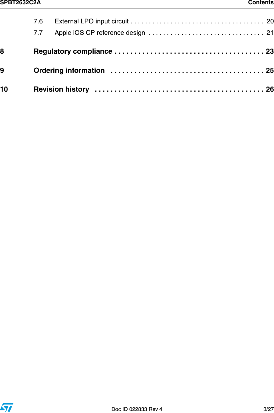
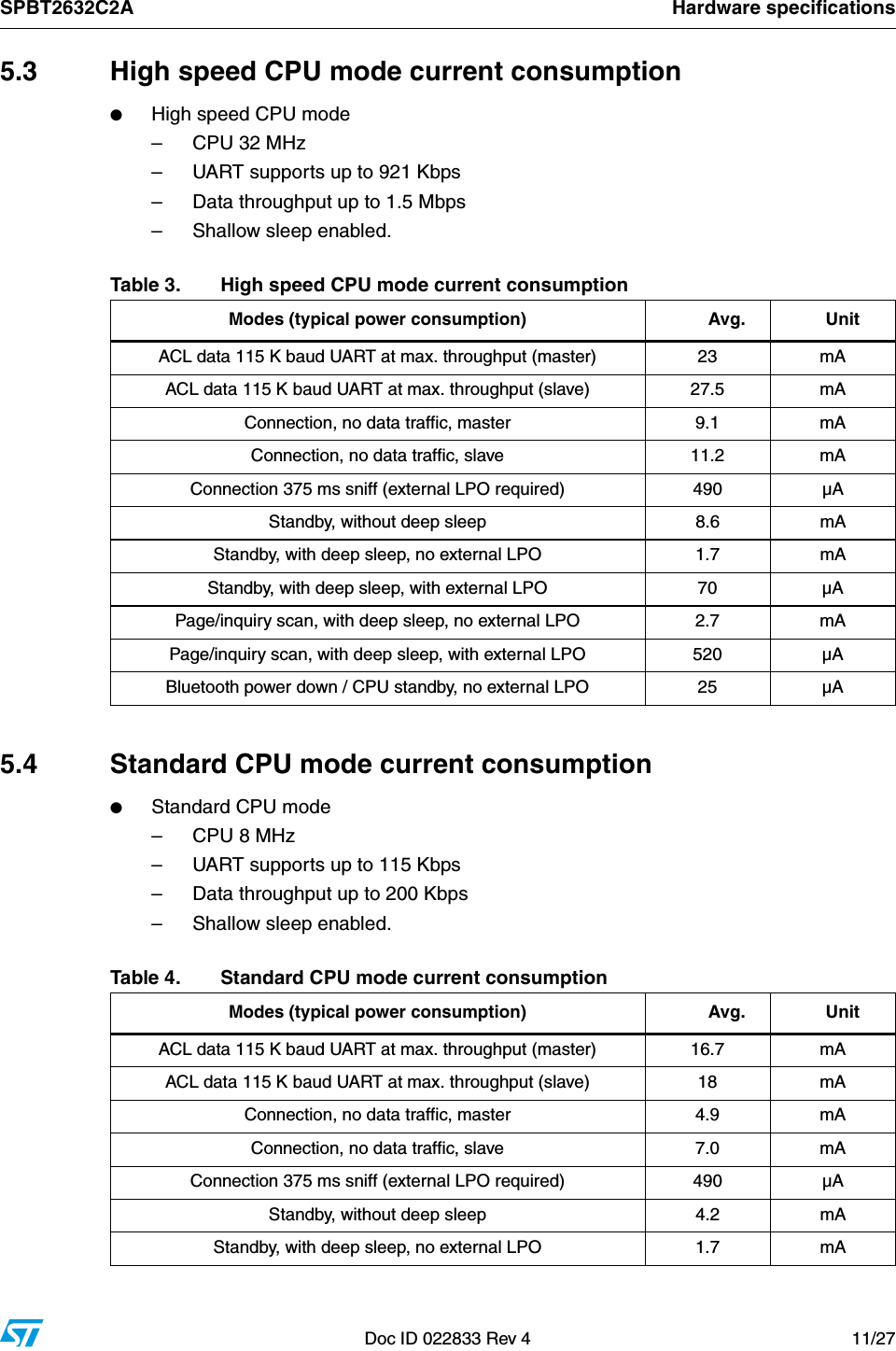
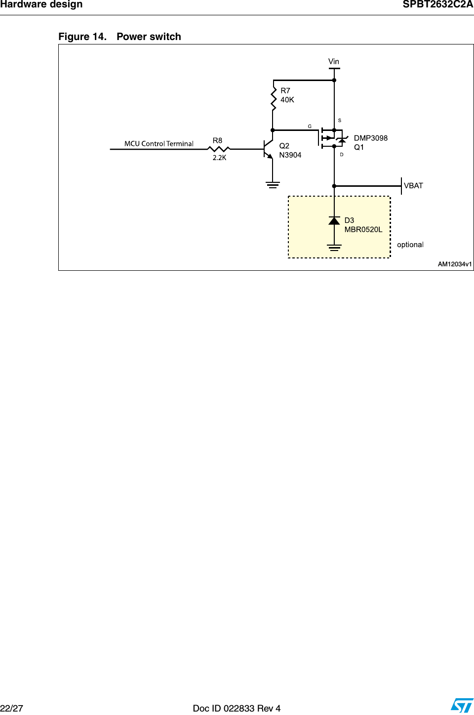
![SPBT2632C2A Hardware specificationsDoc ID 022833 Rev 4 13/275.7 Pin assignmentTable 7. Pin assignmentName Type Pin# Description ALT function(1)1. Please note that the usage of ALT function is dependant upon the firmware that is loaded into the module, and is beyond the scope of this document. The AT command interface uses the main UART by default.5 V tolerantUART interfaceRXD I 13 Receive data ADC 3 YTXD O 14 Transmit data ADC 2 YRTS O 12 Request to send (active low) ADC 0 I2C clock/aux UART Rx YCTS I 11 Clear to send (active low) ADC 1 I2C data/aux UART Tx YBoot loaderBoot 0 I 9 Boot 0Power and groundVin 8 VinGND 7 GNDResetRESETN I 10 Reset input (active low for 5 ms) 2.5 V max.LPOLPO I 15 LPO inputGPIO - general purpose input/outputGPIO [1] I/O 1 General purpose input/output SPI MISO YGPIO [2] I/O 2 General purpose input/output SPI MOSI/I2S_SD YGPIO [3] I/O 3 General purpose input/output SPI SCLK/I2S_CK YGPIO [4] I/O 4 General purpose input/output SPI SS/I2S_WS YGPIO [5] I/O 5 General purpose input/output YGPIO [6] I/O 6 General purpose input/output DAC YGPIO [7] I/O 16 General purpose input/output ADC 4 Y](https://usermanual.wiki/JL-MARINE-SYSTEMS/EA041.Bluetooth-Module/User-Guide-2140937-Page-13.png)
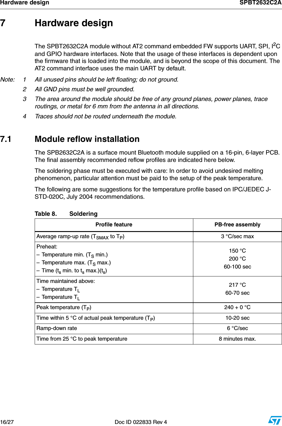
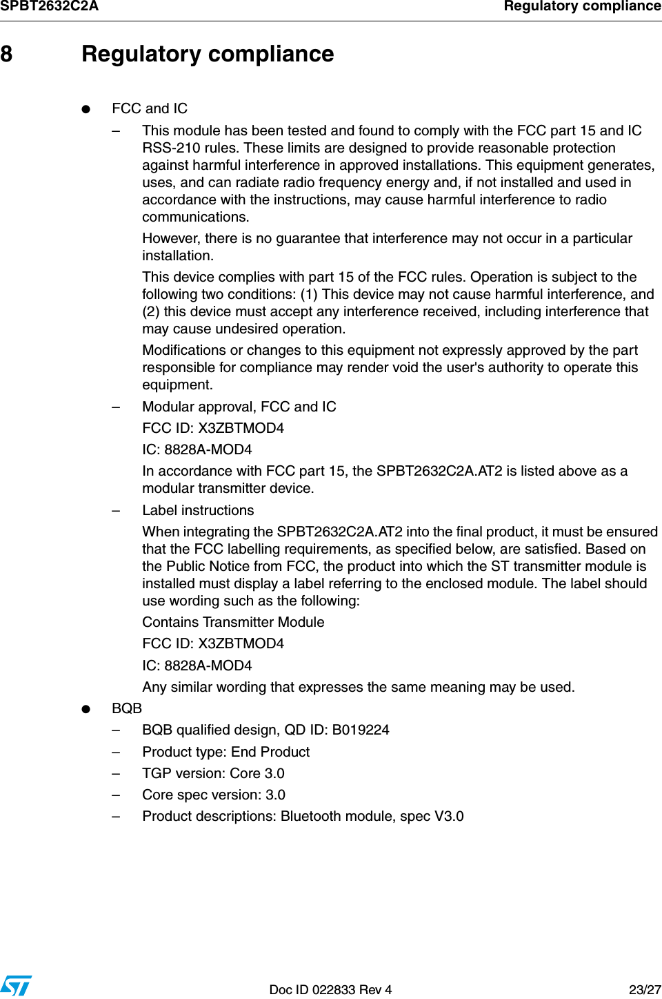
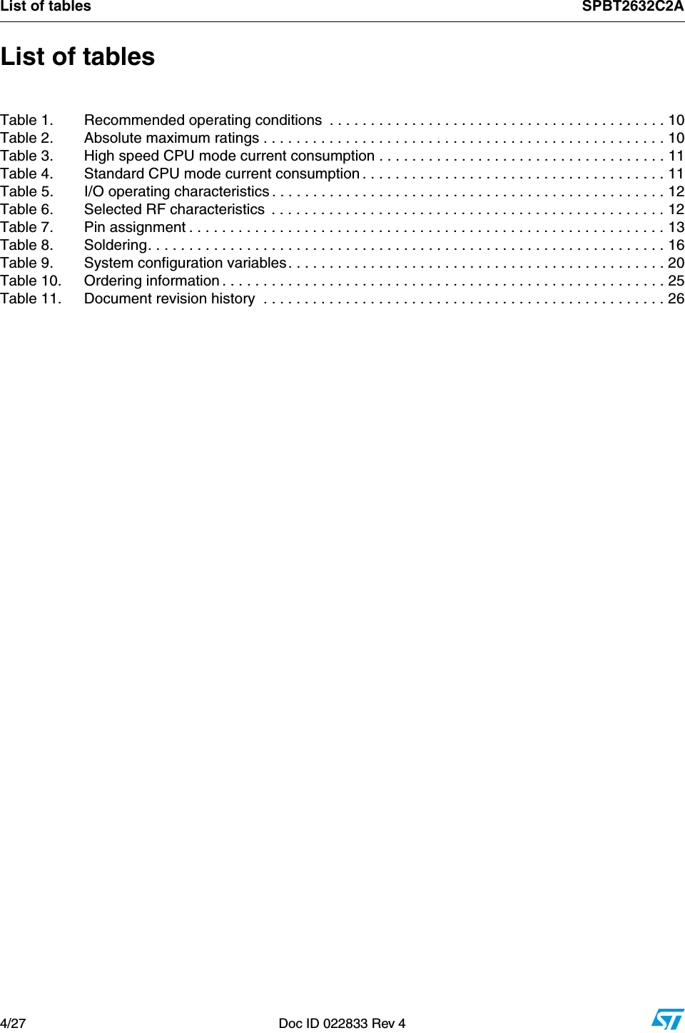
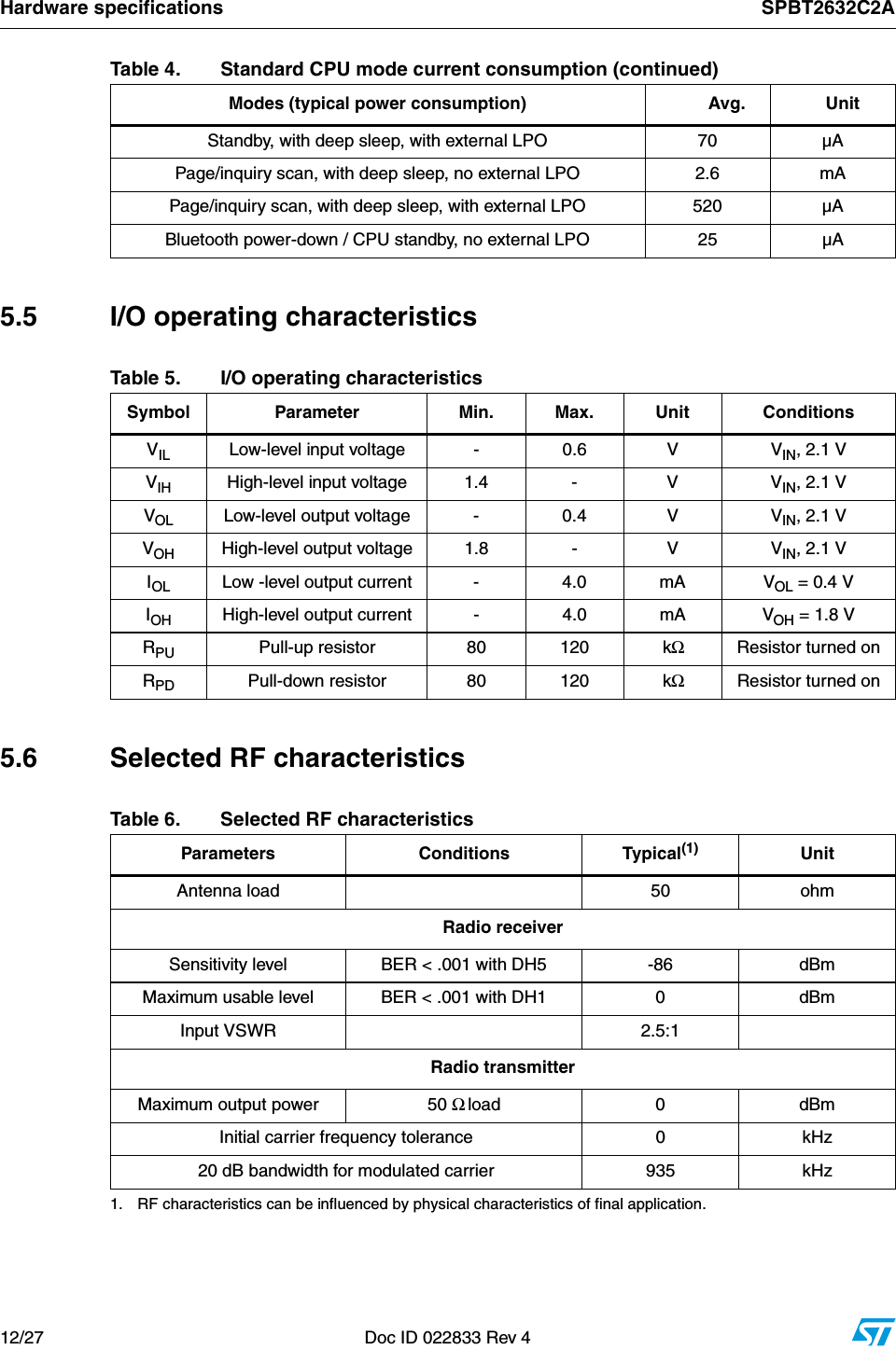
![SPBT2632C2A Hardware designDoc ID 022833 Rev 4 17/27Figure 5. Soldering profile7.2 GPIO interfaceAll GPIOs are capable of sinking and sourcing 4 mA of I/O current. GPIO [1] to GPIO [7] are internally pulled down with 100 kΩ (nominal) resistors.7.3 UART interfaceThe UART is compatible with the 16550 industry standard. Four signals are provided with the UART interface. The TXD and RXD pins are used for data while the CTS and RTS pins are used for flow control.Figure 6. Connection to host device!-V"LUETOOTH-ODULE(OST!-V](https://usermanual.wiki/JL-MARINE-SYSTEMS/EA041.Bluetooth-Module/User-Guide-2140937-Page-17.png)