Getac Technology RS500 UHF RFID Module User Manual module
Getac Technology Corporation UHF RFID Module module
UserManual.wiki
>
Getac Technology
>
RS500 User Manual
>
User Manual-module
Contents
1.
User Manual-Host
2.
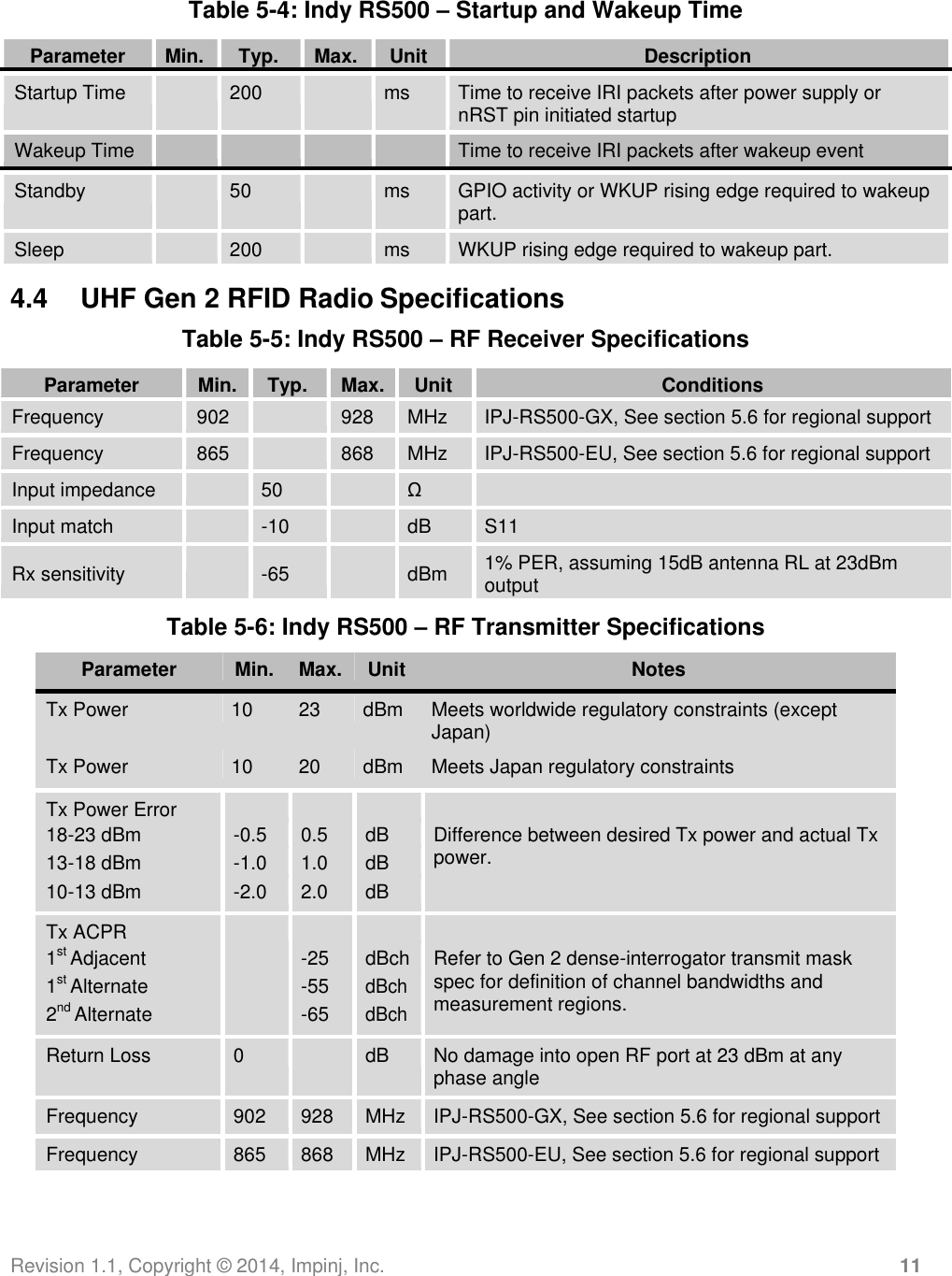
User Manual-module
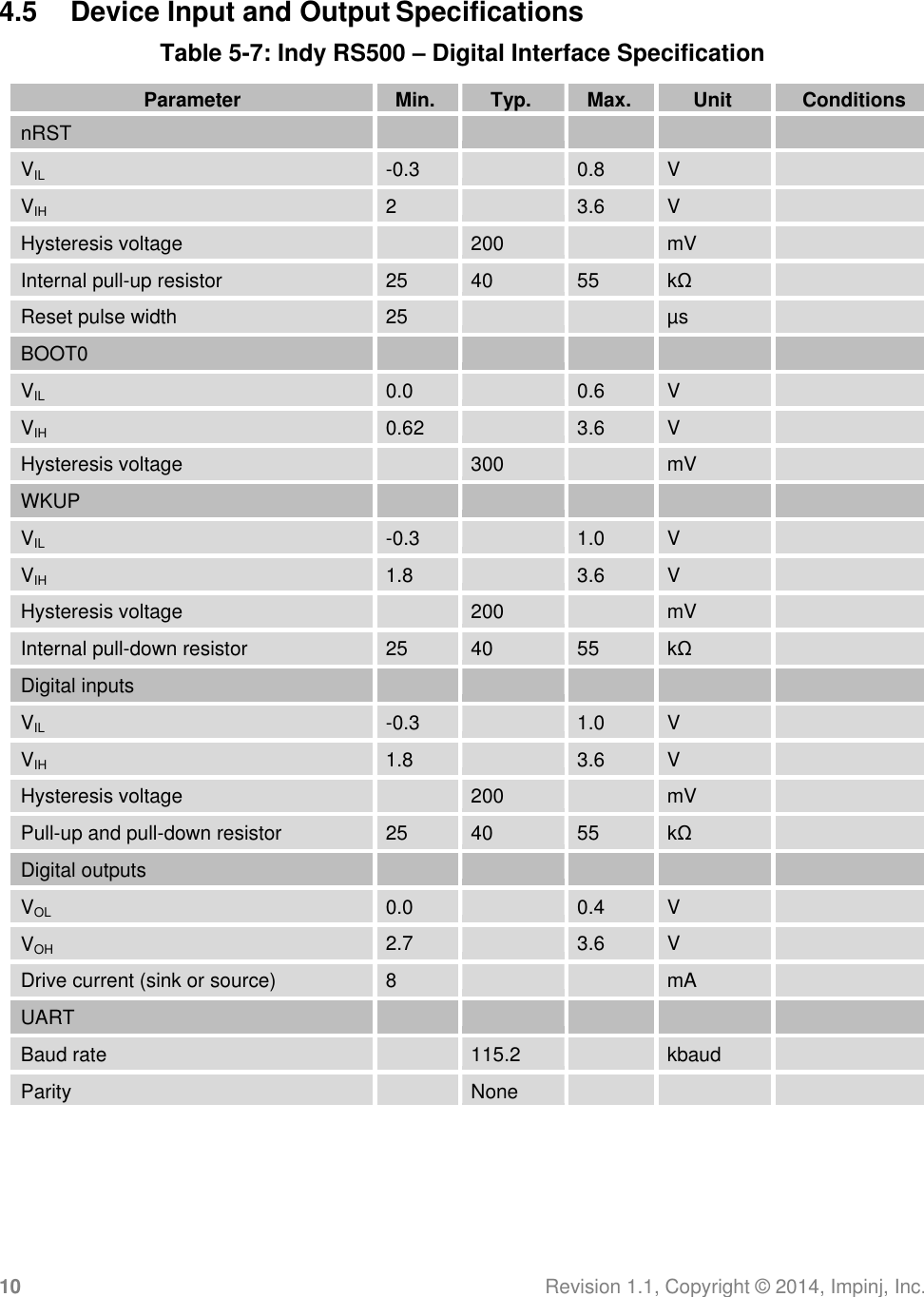
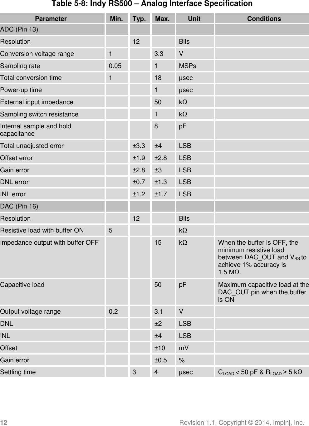
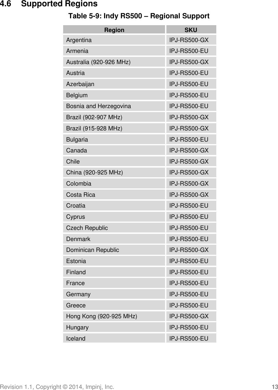
User Manual-module
Navigation menu
Upload a User Manual
Namespaces
Wiki Guide
HTML
PDF
Info
Views
User Manual
Discussion / Help
Navigation