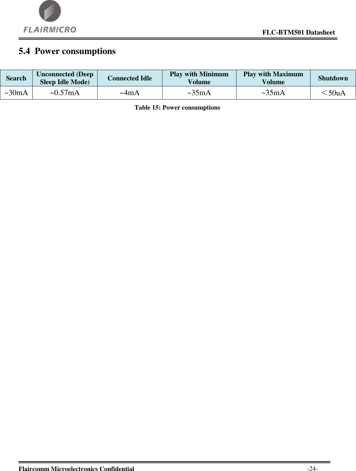
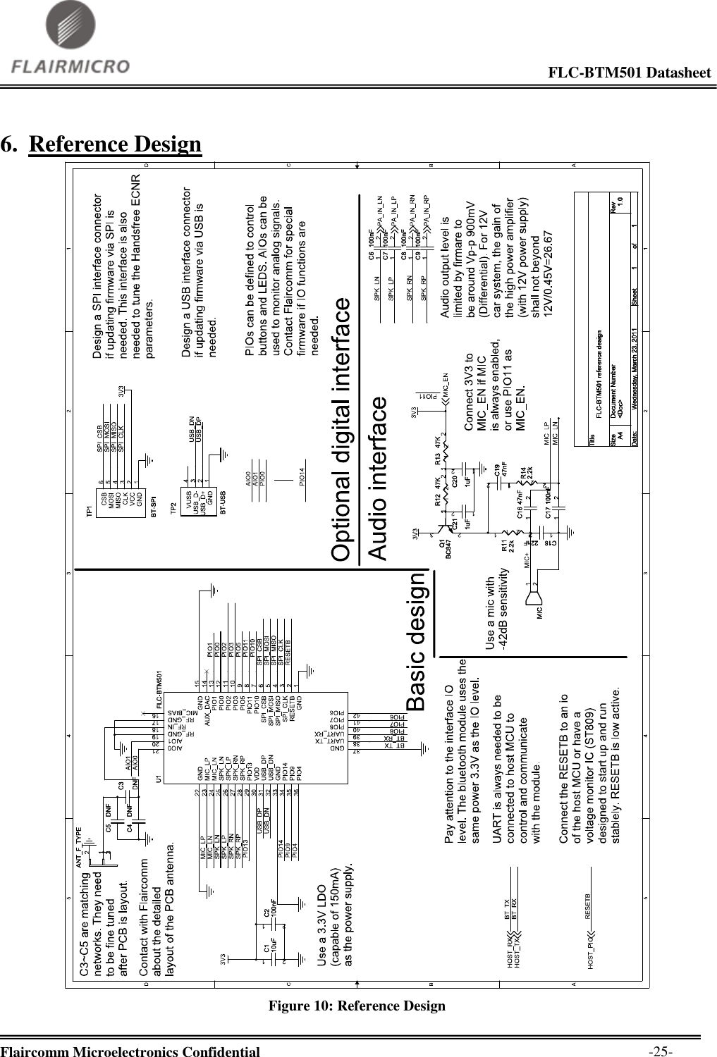
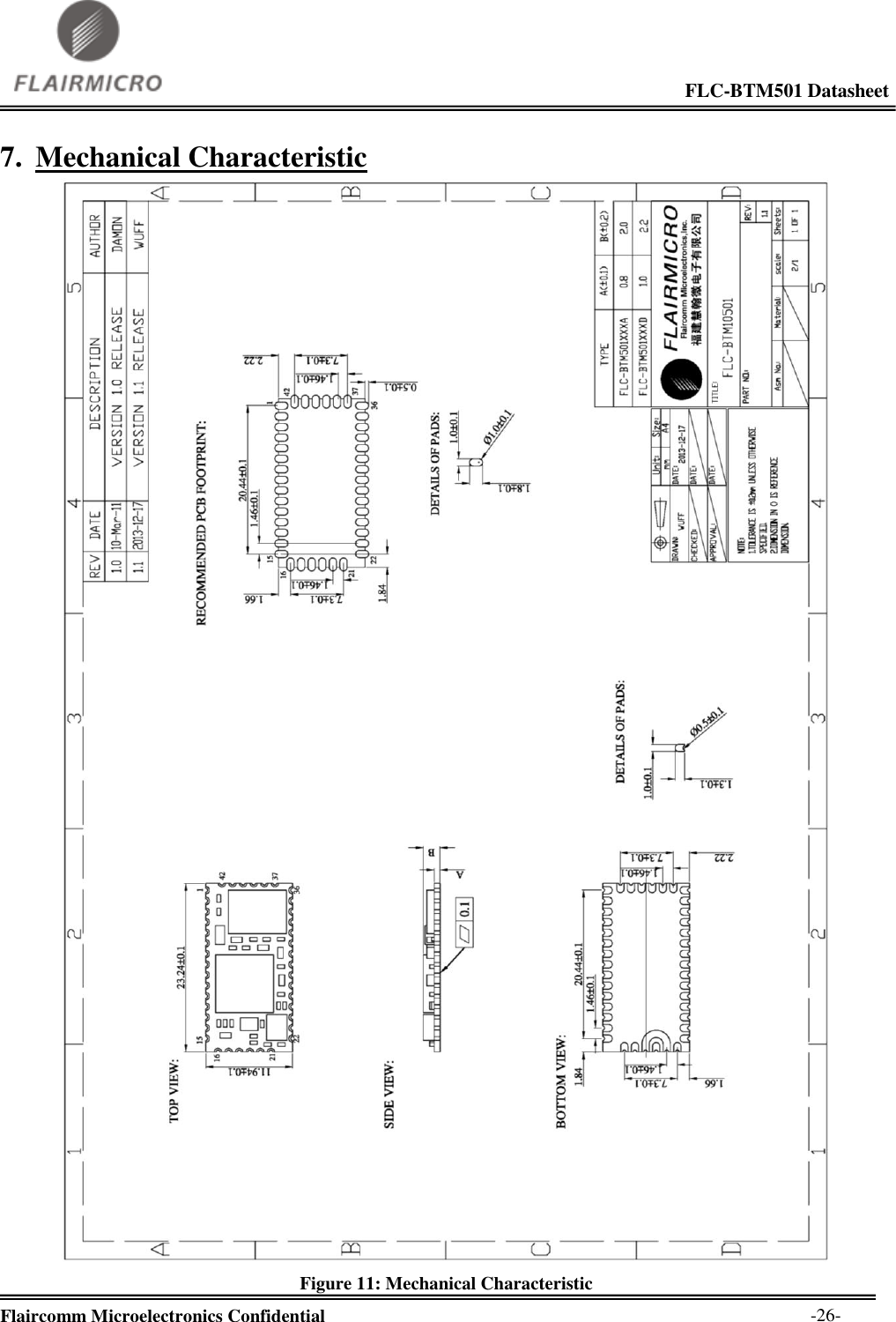
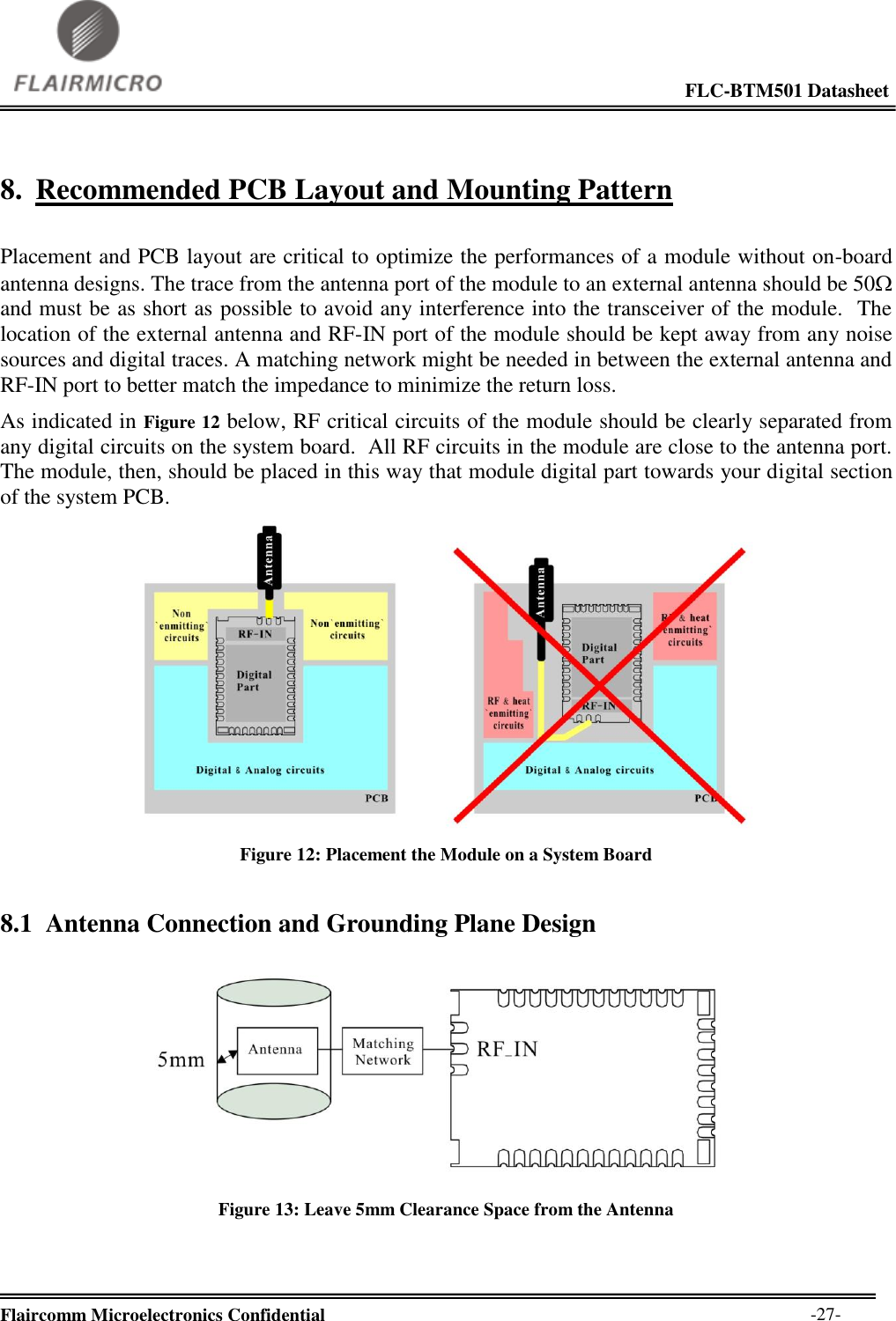
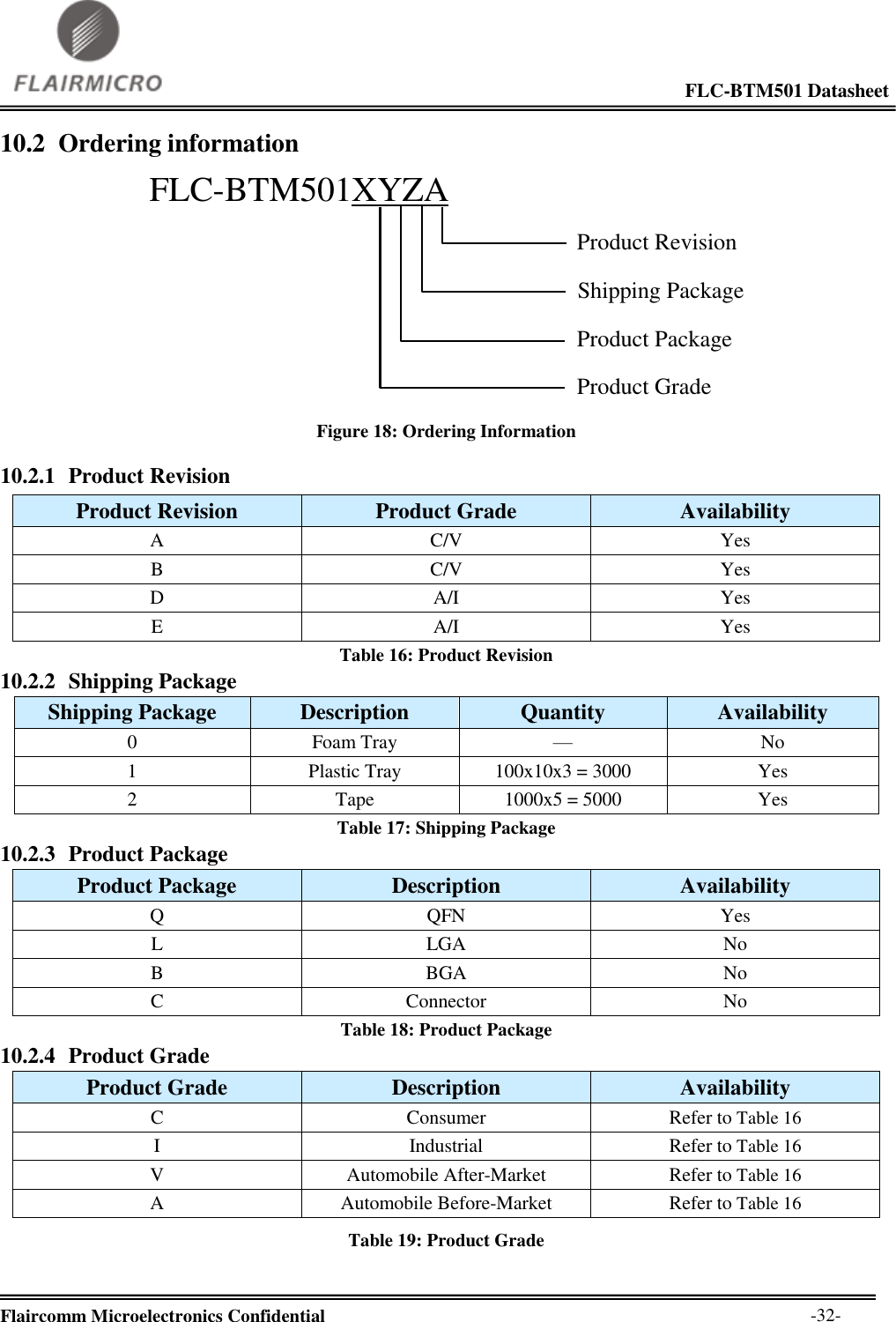
Flaircomm Microelectronics BTM501 Bluetooth Module User Manual FLC BTMxxx DS V1 0
Flaircomm Microelectronics,Inc. Bluetooth Module FLC BTMxxx DS V1 0
UserManual.wiki
>
Flaircomm Microelectronics
>
BTM501 User Manual
User Manual
Navigation menu
Upload a User Manual
Namespaces
Wiki Guide
HTML
PDF
Info
Views
User Manual
Discussion / Help
Navigation
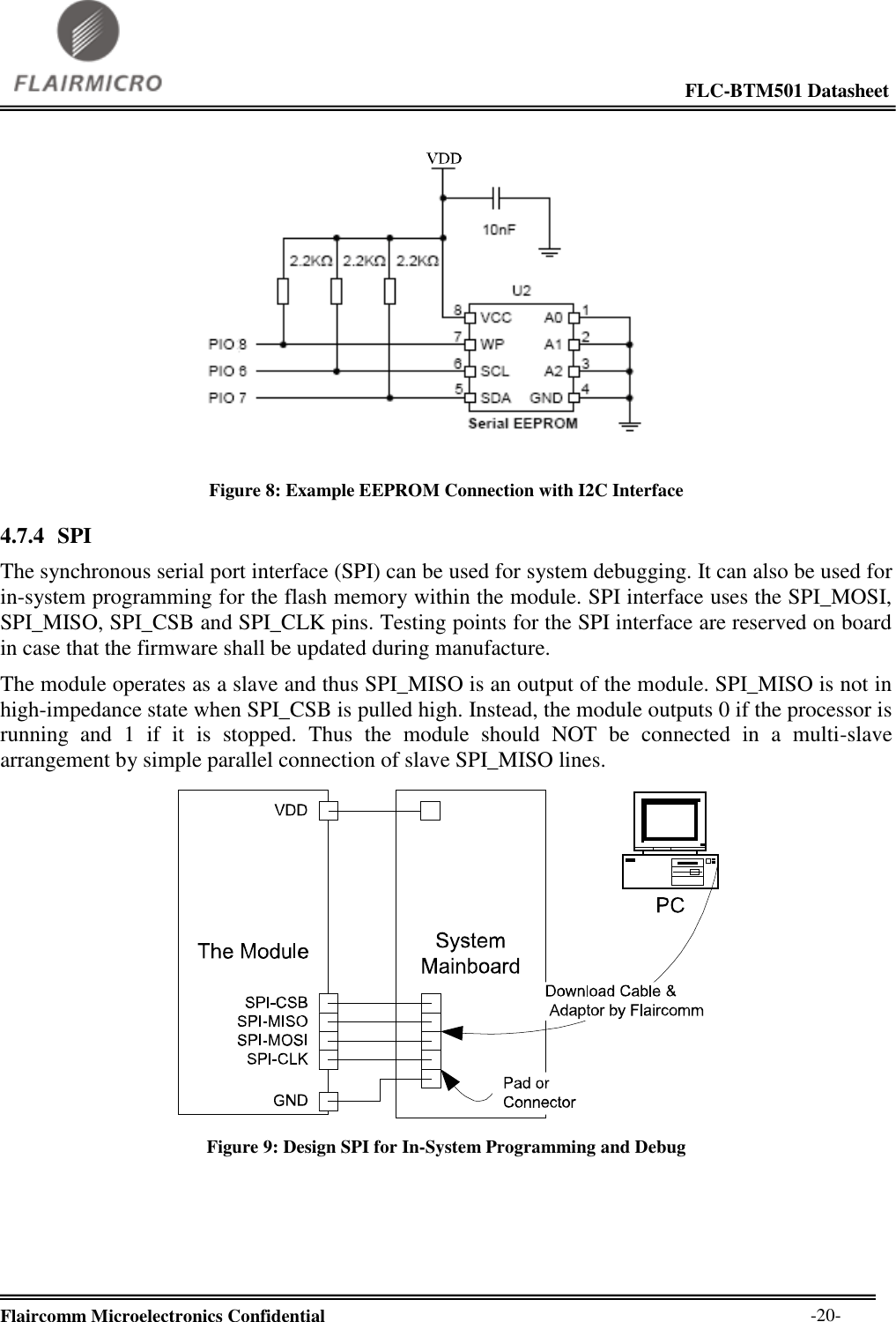
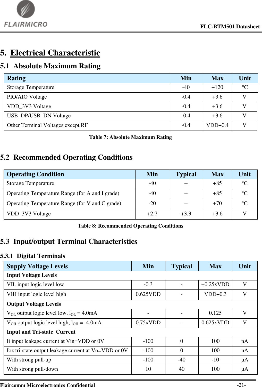
![Flaircomm Microelectronics Confidential 1) The antenna must be installed such that 20 cm is maintained between the antenna and users, and 2) The transmitter module may not be co-located with any other transmitter or antenna. As long as 2 conditions above are met, further transmitter test will not be required. However, the OEM integrator is still responsible for testing their end-product for any additional compliance requirements required with this module installed IMPORTANT NOTE: In the event that these conditions cannot be met (for example certain laptop configurations or co-location with another transmitter), then the FCC authorization is no longer considered valid and the FCC ID cannot be used on the final product. In these circumstances, the OEM integrator will be responsible for reevaluating the end product(including the transmitter) and obtaining a separate FCC authorization. End Product Labeling This transmitter module is authorized only for use in device where the antenna may be installed such that 20 cm may be maintained between the antenna and users. The final end product must be labeled in a visible area with the following: “Contains FCC ID: P4I-BTM501”. The grantee's FCC ID can be used only when all FCC compliance requirements are met. Manual Information to the End User The OEM integrator has to be aware not to provide information to the end user regarding how to install or remove this RF module in the user’s manual of the end product which integrates this module. The end user manual shall include all required regulatory information/warning as show in this manual. 11.3 Industry Canada statement This Class B digital apparatus complies with Canadian ICES-003. Cet appareil numérique de la classe [*] est conforme à la norme NMB-003 du Canada. This device complies with Industry Canada’s licence-exempt RSS standard(s). Operation is subject to the following two conditions: (1) This device may not cause interference; and (2) This device must accept any interference, including interference that may cause undesired operation of the device. Le présent appareil est conforme aux CNR d’Industrie Canada applicables aux appareils radio exempts de licence. L’exploitation est autorisée aux deux conditions suivantes : 1) l’appareil ne doit pas produire de brouillage; 2) l’appareil doit accepter tout brouillage radioélectrique subi, même si le brouillage est susceptible d’en compromettre le fonctionnement. Radiation Exposure Statement: This equipment complies with IC radiation exposure limits set forth for an uncontrolled environment. This equipment should be installed and operated with minimum distance 20cm between the radiator & your body. Déclaration d'exposition aux radiations: Cet équipement est conforme aux limites d'exposition aux rayonnements IC établies pour un environnement non contrôé. Cet équipement doit être installé et utilisé avec un minimum de 20cm de distance entre la source de rayonnement et votre corps. This device is intended only for OEM integrators under the following conditions: 1) The antenna must be installed such that 20 cm is maintained between the antenna and users, and 2) The transmitter module may not be co-located with any other transmitter or antenna.](https://usermanual.wiki/Flaircomm-Microelectronics/BTM501/User-Guide-3132350-Page-34.png)