Flaircomm Microelectronics BTM101 Bluetooth module User Manual FLC BTM401 DS
Fujian Flaircomm Microelectronics,Inc. Bluetooth module FLC BTM401 DS
UserManual.wiki
>
Flaircomm Microelectronics
>
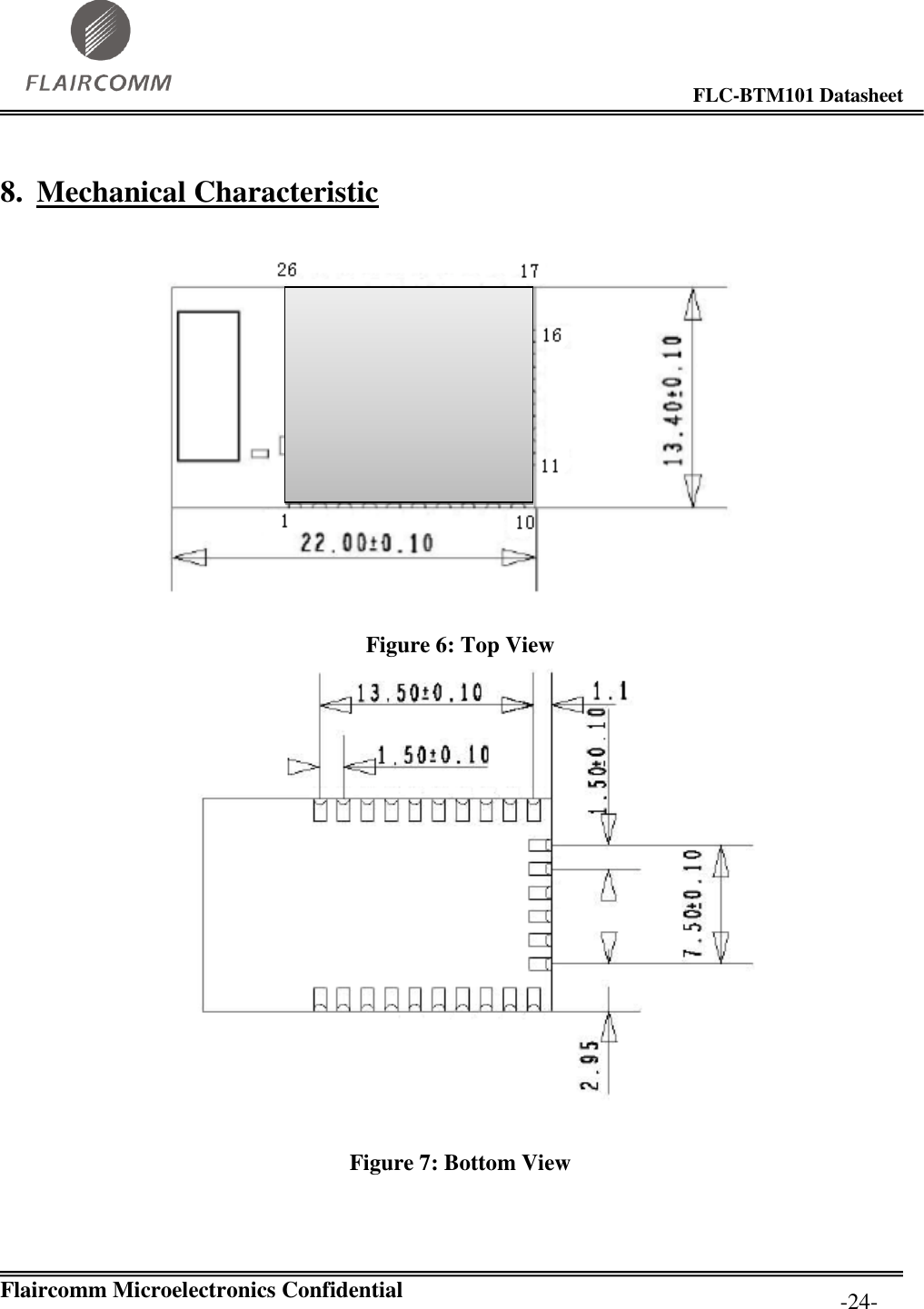
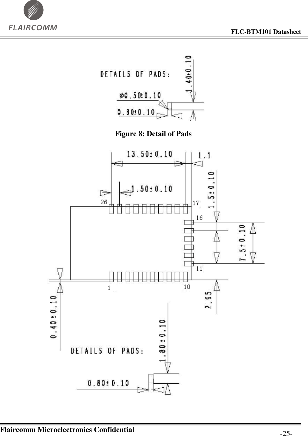
BTM101 User Manual
User Manual
Navigation menu
Upload a User Manual
Namespaces
Wiki Guide
HTML
PDF
Info
Views
User Manual
Discussion / Help
Navigation
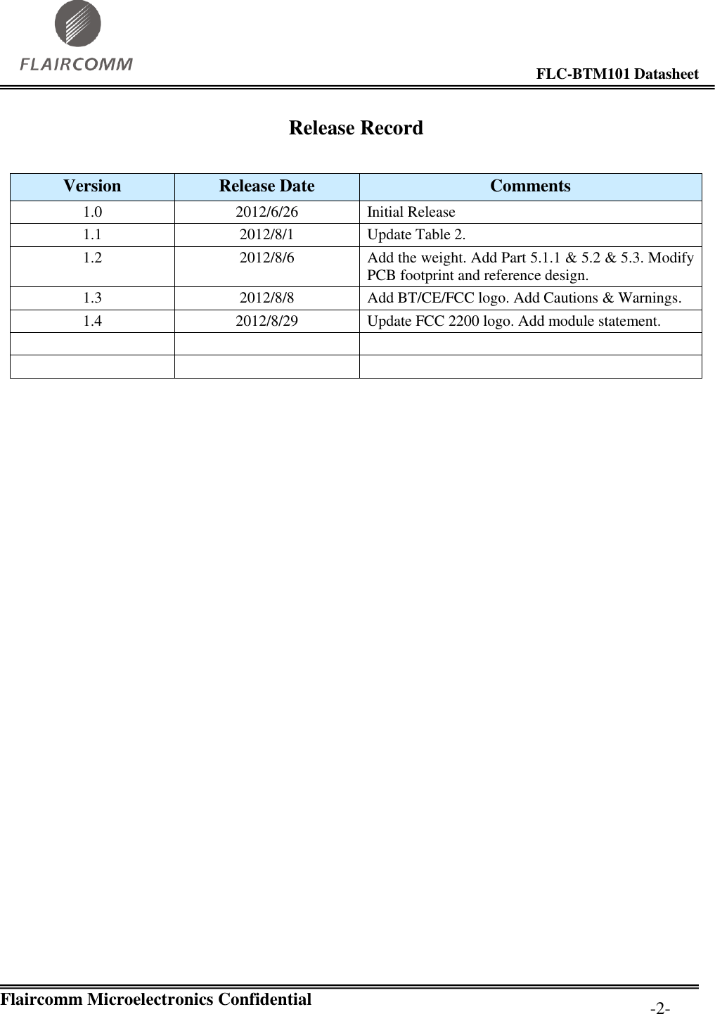
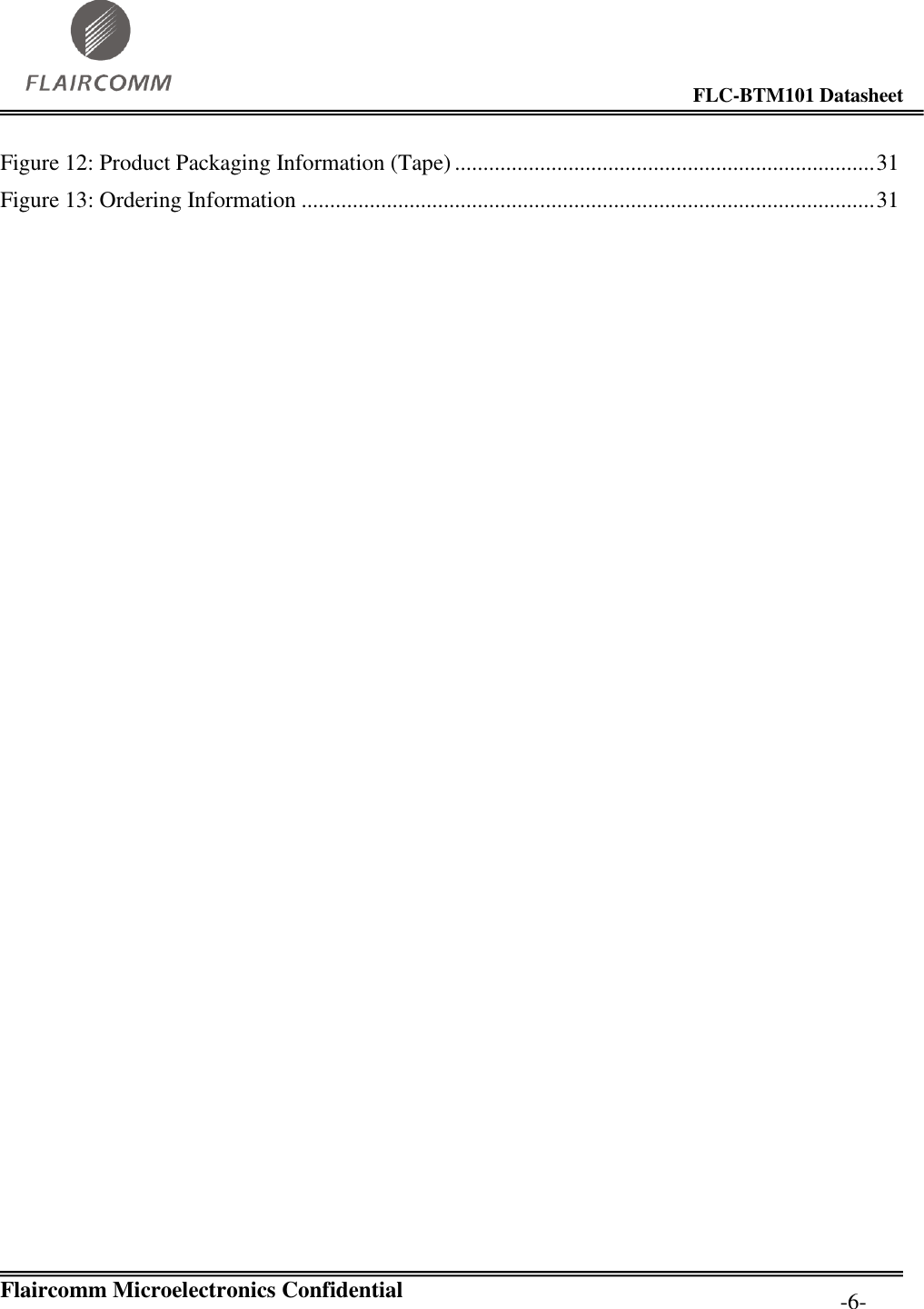
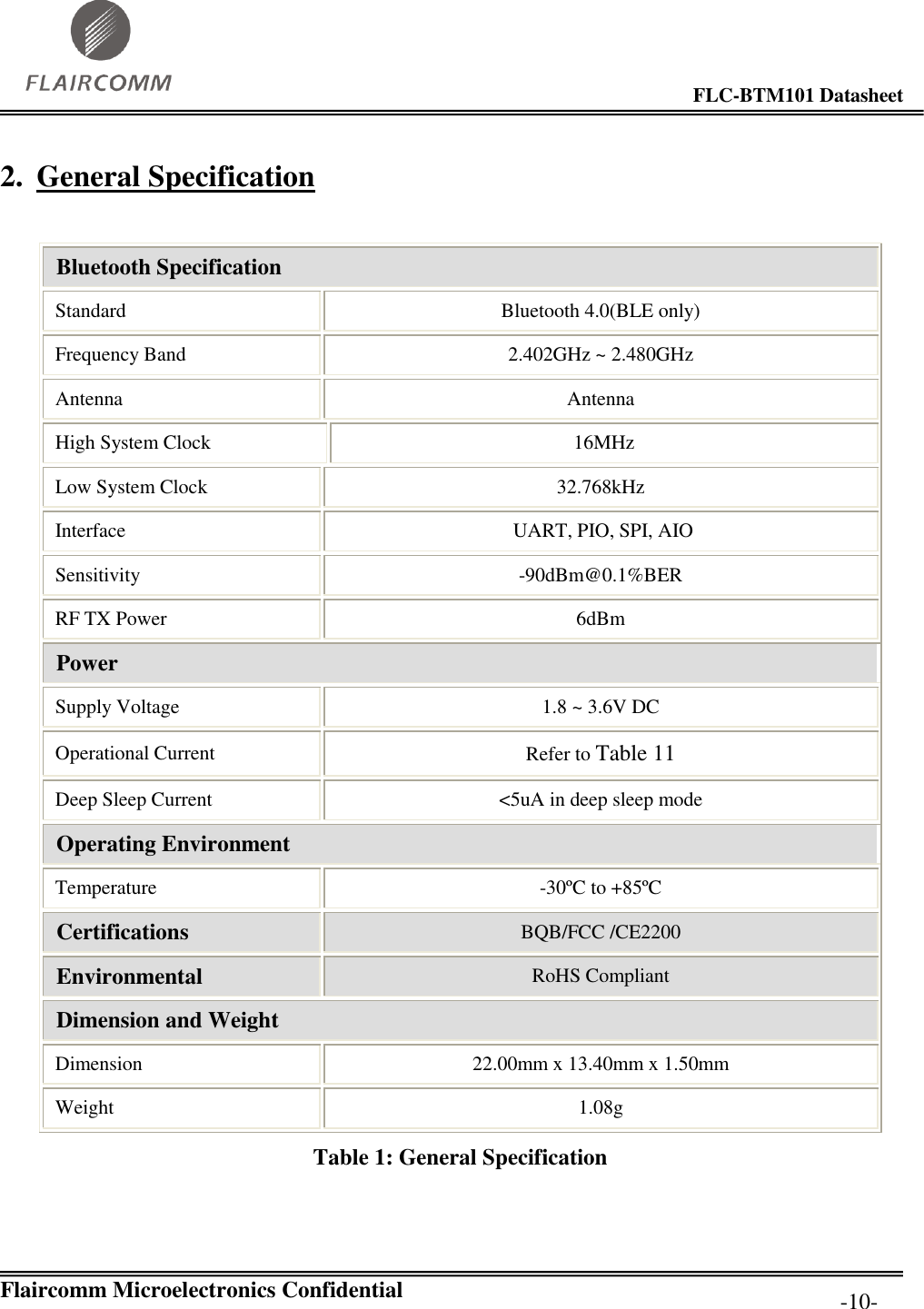
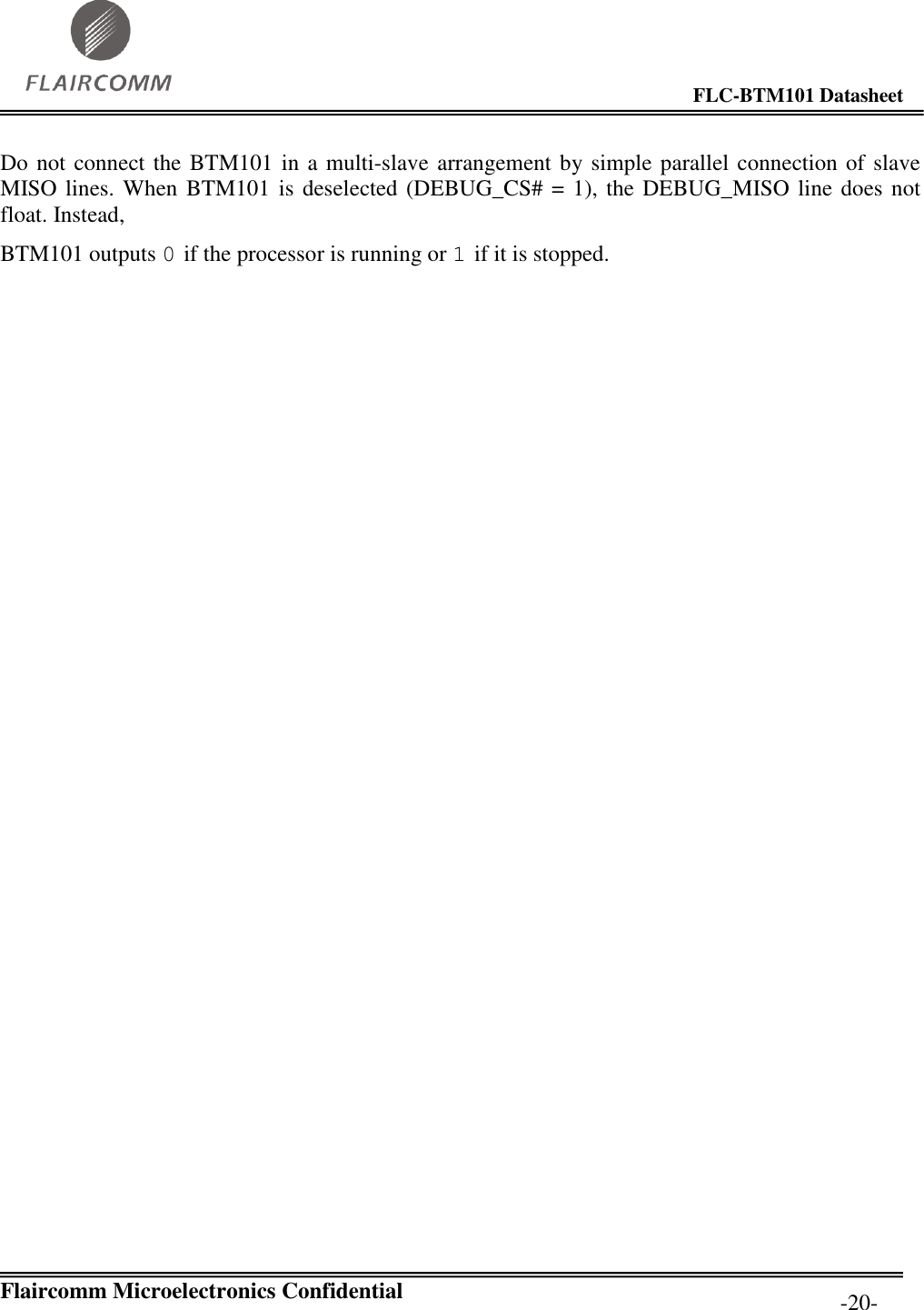
![FLC-BTM101 Datasheet Flaircomm Microelectronics Confidential -13- 19 PIO10 Bi-directional with programmable strength internal pull-up/down Programmable input/output line 20 VDD_PIO Power Input Positive supply for all digital I/O port PIO[11:0] 21 PIO11 Bi-directional with programmable strength internal pull-up/down Programmable input/output line 22 SPI_PIO#SEL Input with strong internal pull-down Select SPI debug port on PIO[8:5] 23 Wake-up Input has no internal pull-up or pull-down, use external pull-down Input to wake up BTM101 from hibernate 24 VDD Power input 3.3v power input 25 GND Ground Ground 26 GND Ground Ground Table 2: Pin Definition](https://usermanual.wiki/Flaircomm-Microelectronics/BTM101/User-Guide-1783759-Page-13.png)
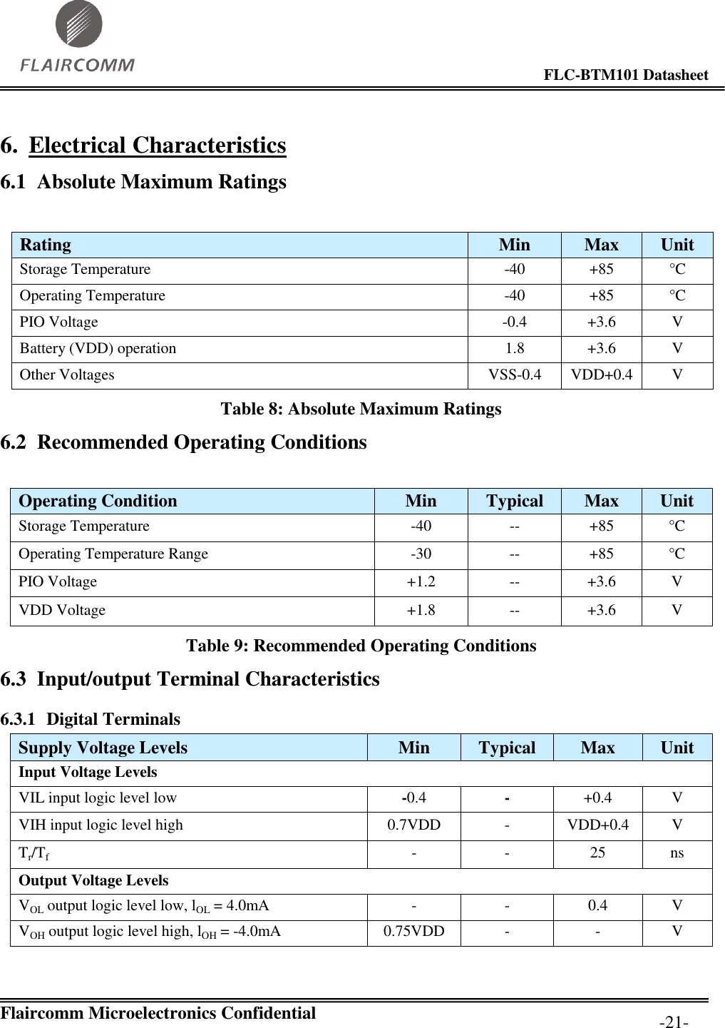
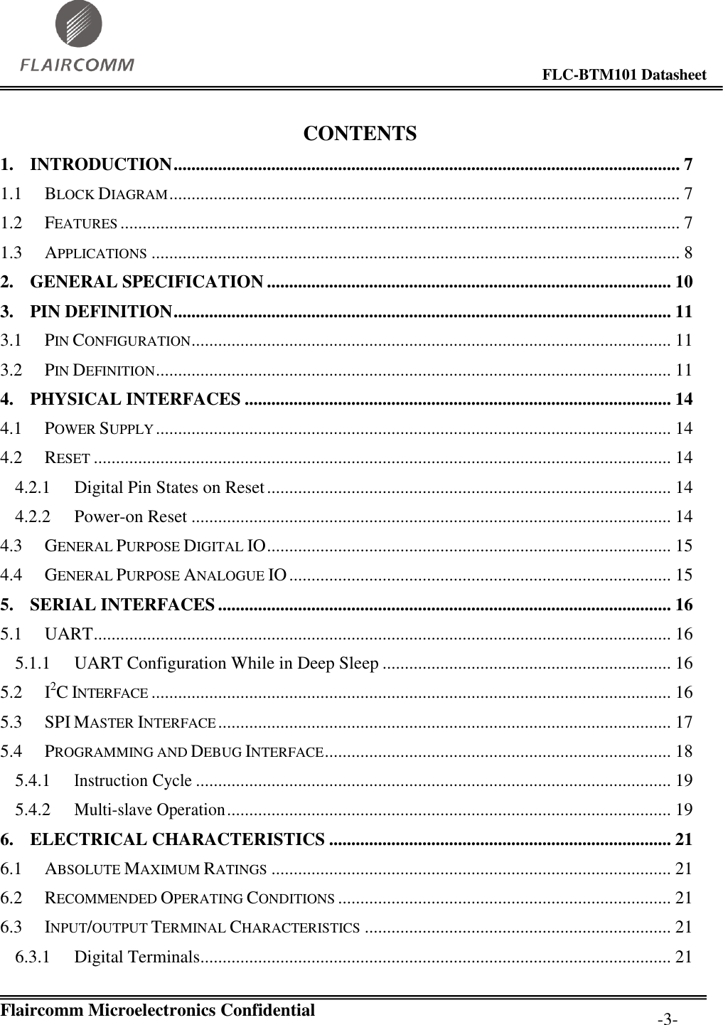
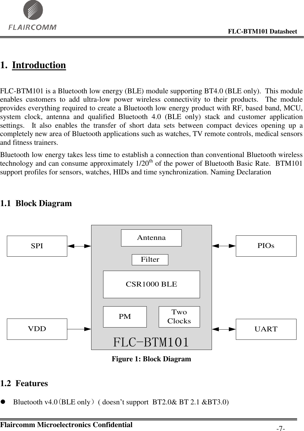
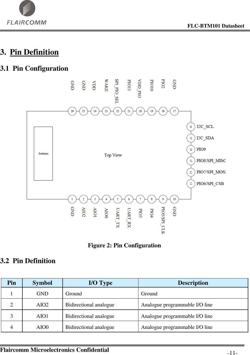
![FLC-BTM101 Datasheet Flaircomm Microelectronics Confidential -14- 4. Physical Interfaces 4.1 Power Supply BTM101 contains two regulators: One switch-mode regulator, which generates the main supply rail directly from battery One low-voltage linear regulator with 1.2V output powers digital circuits VDD_PIO is input voltage to power all digital I/Os including PIOs, UART port, SPI port and I2C. 4.2 Reset The module may be reset from several sources: Power-on reset Software configured watchdog timer. 4.2.1 Digital Pin States on Reset The following table shows the digital pin states of BTM101 on reset. PU and PD default to weak values unless specified otherwise. Pin Name / Group On Reset I2C_SDA Strong PU I2C_SCL Strong PU PIO[11:0] Weak PD Table 3: Digital Pin Status on Reset 4.2.2 Power-on Reset The following table shows how the power-on reset occurs.](https://usermanual.wiki/Flaircomm-Microelectronics/BTM101/User-Guide-1783759-Page-14.png)
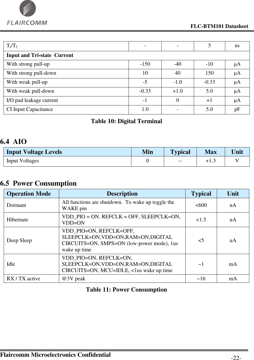
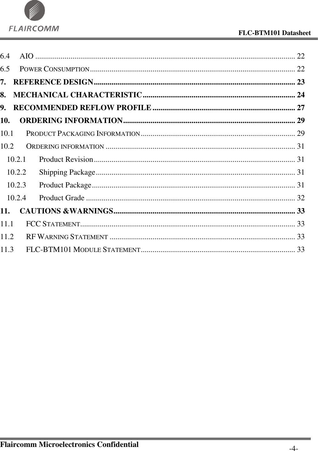
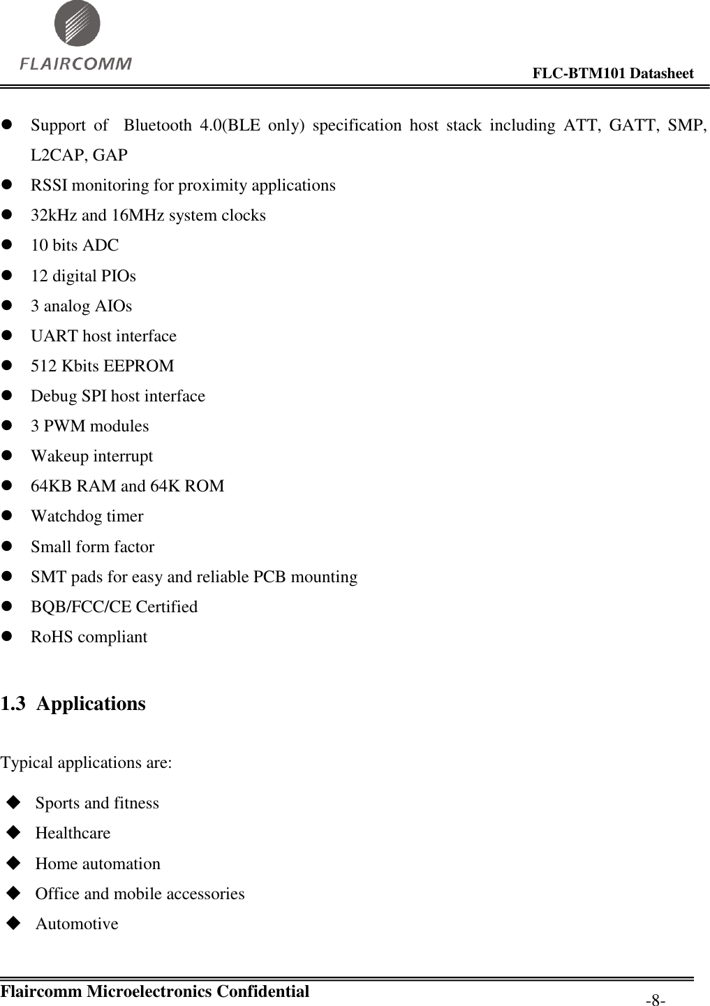
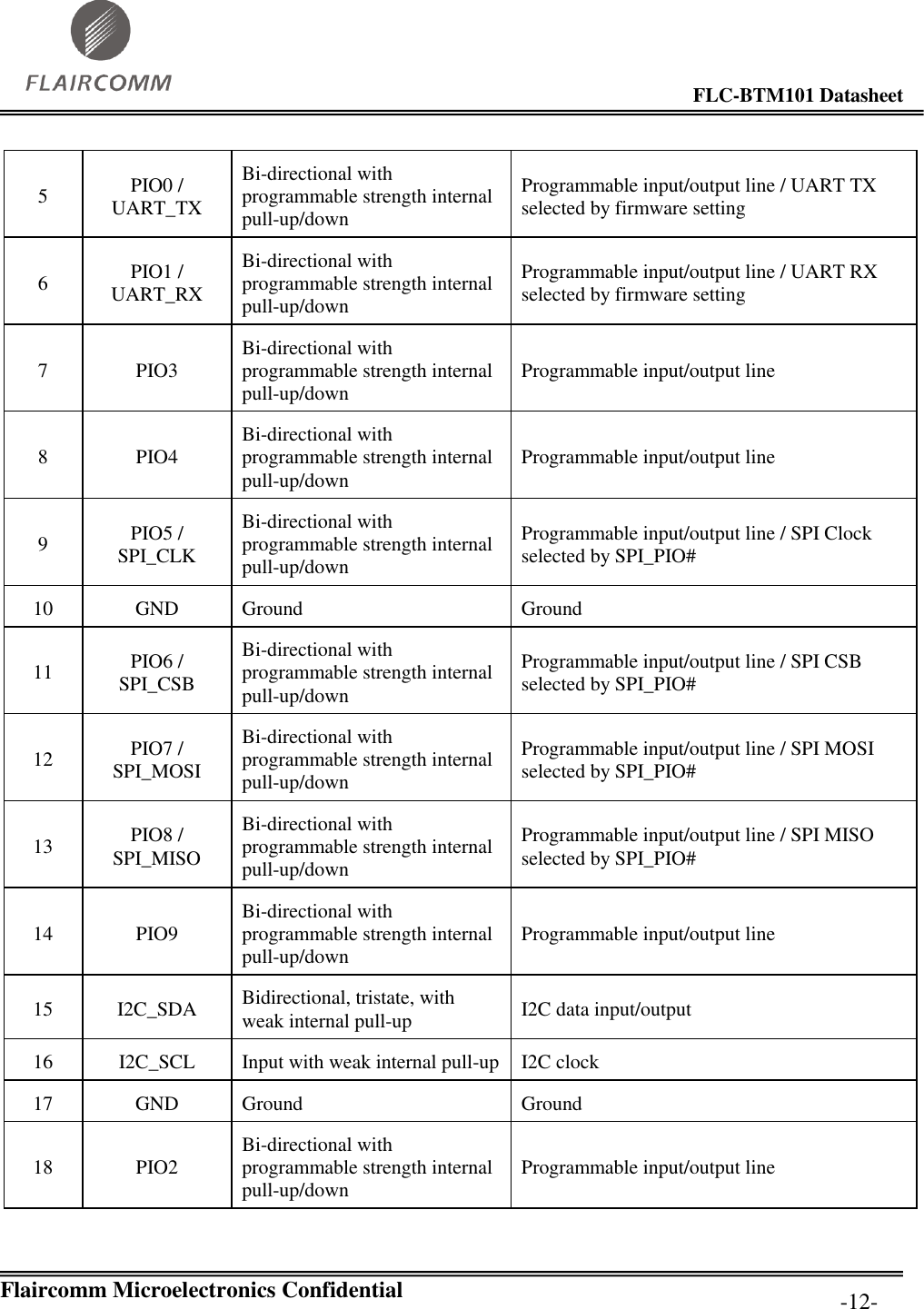
![FLC-BTM101 Datasheet Flaircomm Microelectronics Confidential -15- Power-on Reset Type Unit Reset release on VDD_DIG rising 1.05 V Reset assert on VDD_DIG falling 1.00 Reset assert on VDD_DIG falling (Sleep mode) 0.60 Hysteresis 50 mV Table 4: Power-on Reset 4.3 General Purpose Digital IO 12 lines of programmable bidirectional I/O are provided. They are all powered from VDD_PIO. PIO lines are software configurable as weak pull-up, weak pull-down, strong pull-up or strong pull-down. NOTE: at reset all PIO lines are input with weak pull-downs. Any of the PIO line can be configured as interrupt request line or as weak-up lines from sleep modes. The BTM101 supports alternative functions on the PIO lines: SPI interface, UART. LED flashing / PWM module. NOTE: Implementation of the PIO lines is firmware build specific. 4.4 General Purpose Analogue IO BTM101 has 3 general purpose analog interface pins, AIO [2:0].](https://usermanual.wiki/Flaircomm-Microelectronics/BTM101/User-Guide-1783759-Page-15.png)
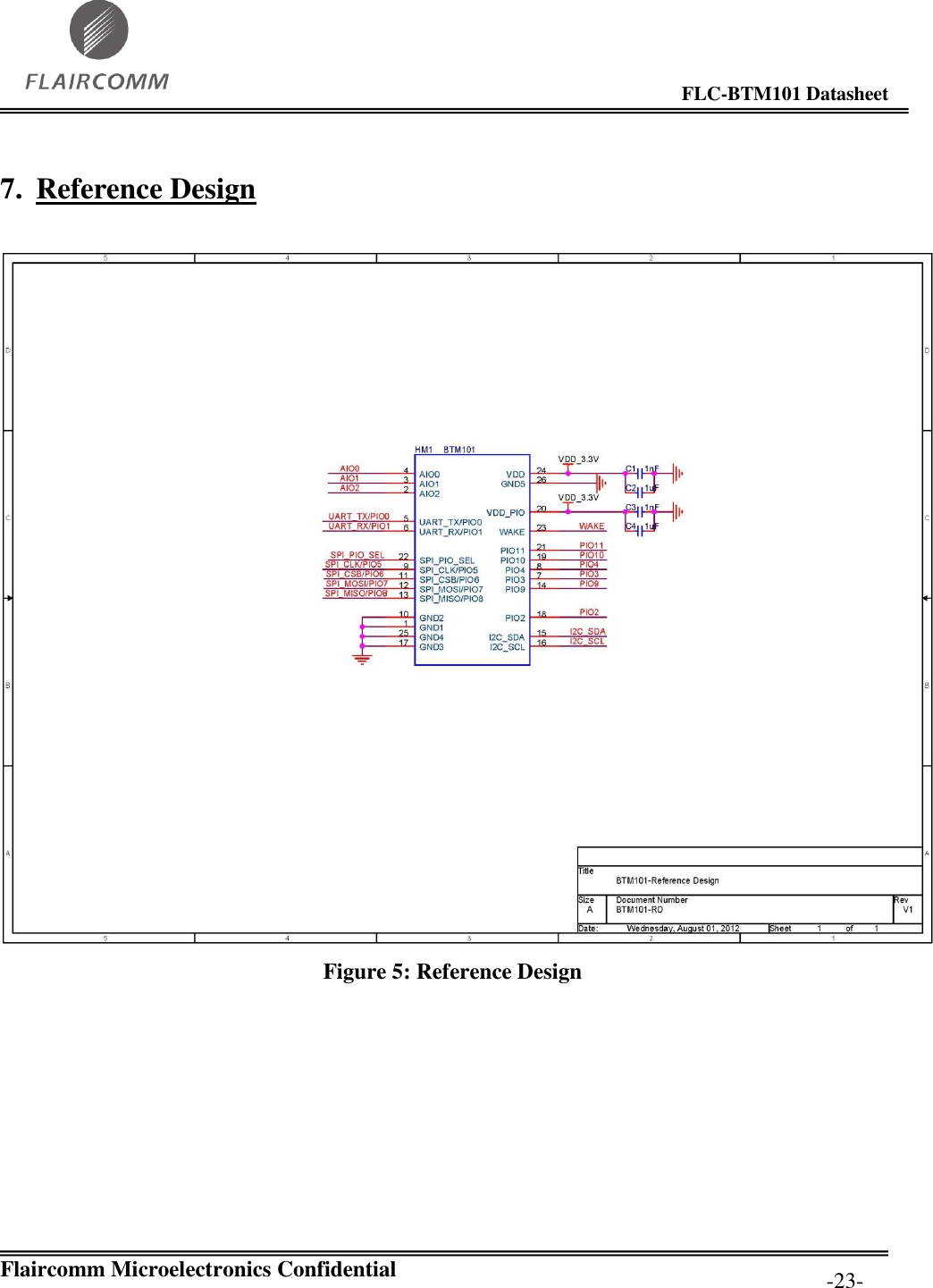
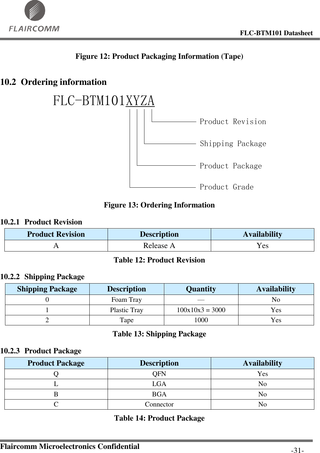
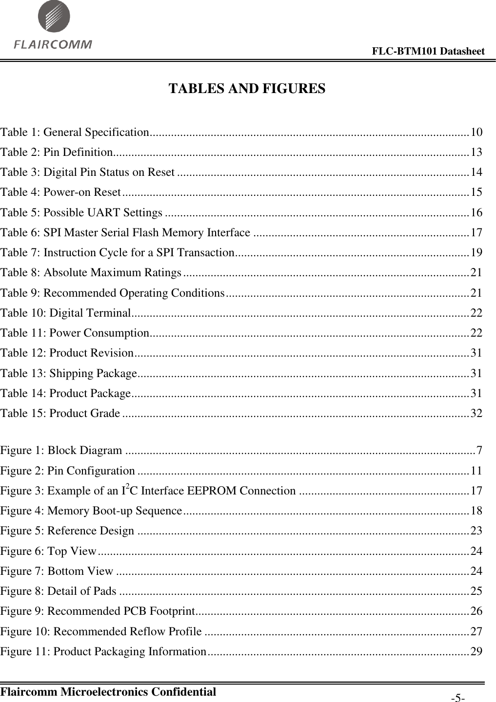
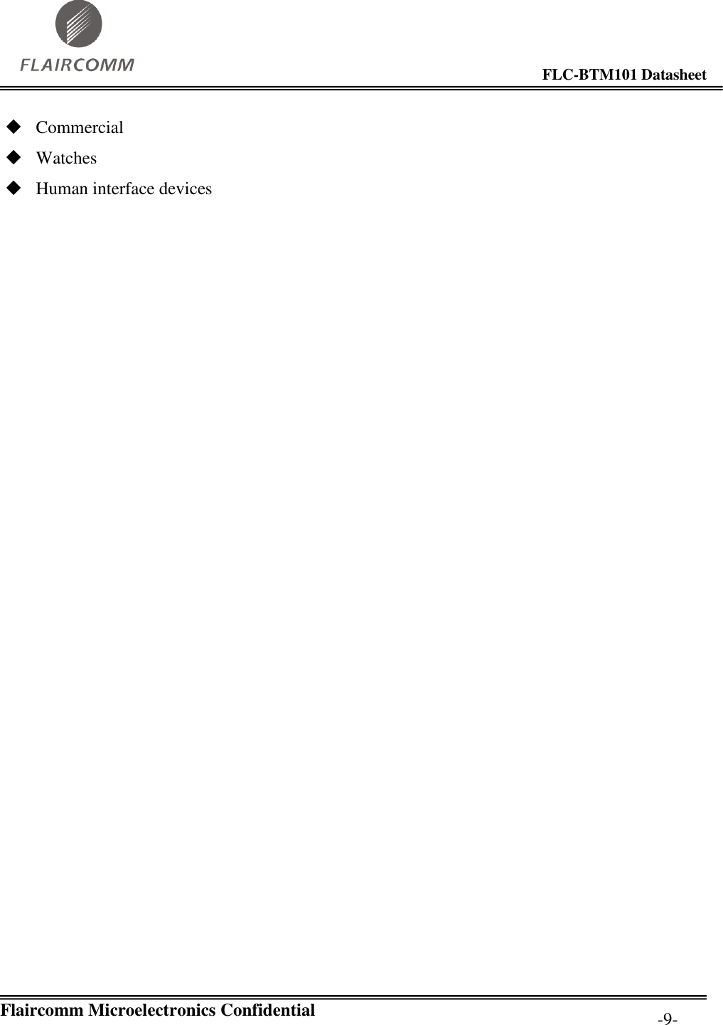
![FLC-BTM101 Datasheet Flaircomm Microelectronics Confidential -16- 5. Serial Interfaces 5.1 UART This is a standard UART interface for communicating with other serial devices. The UART interface provides a simple mechanism for communicating with other serial devices using the RS232 protocol. When the module is connected to another digital device, UART_RX and UART_TX transfer data between the two devices. When selected in firmware PIO[0] is assigned to UART_TX and PIO[1] is assigned to UART_RX. The UART CTS and RTS signals can be assigned to any PIO pin by the on-chip firmware. Parameter Possible Values Baud Rate Minimum 1200 baud (≤2%Error) 9600 baud (≤1%Error) Maximum 4M baud (≤1%Error) Flow control CTS / RTS Parity None, Odd or Even Number of Stop Bits 1 or 2 Bits per Byte 8 Table 5: Possible UART Settings 5.1.1 UART Configuration While in Deep Sleep The maximum baud rate is 9600 baud during deep sleep. 5.2 I2C Interface The I2C interface communicates to an internal EEPROM, or external peripherals or sensors. The internal EEPROM holds the program code inside BTM101. Figure 3 shows the connection of the internal EEPROM with the I2C interface where I2C_SCL, I2C_SDA and PIO [2] are connected to the internal EEPROM. The PIO [2] pin supplies the power to the EEPROM supply pin, e.g. VDD. At boot-up, if there is no valid ROM image in the BTM101 ROM area, BTM101 tries to boot from the I2C interface, see Figure 4. This involves reading the code from the internal EEPROM and loading it into the internal BTM101 RAM.](https://usermanual.wiki/Flaircomm-Microelectronics/BTM101/User-Guide-1783759-Page-16.png)
![FLC-BTM101 Datasheet Flaircomm Microelectronics Confidential -17- Figure 3: Example of an I2C Interface EEPROM Connection 5.3 SPI Master Interface BTM101 provides a SPI interface to connect an external serial flash memory. The SPI master memory interface in the BTM101 is overlaid on the I2C interface and uses a further 3 PIOs for the extra pins, see Table 6. SPI Interface Pin Flash_VDD PIO[2] SF_DIN PIO[3] SF_CS# PIO[4] SF_CLK I2C_SCL SF_DOUT I2C_SDA Table 6: SPI Master Serial Flash Memory Interface Note: If an application using BTM101 is designed to boot from SPI serial flash, it is possible for the firmware to map the I2C interface to alternative PIOs. The boot-up sequence for BTM101 is controlled by hardware and firmware. Figure 4 shows the sequence of loading RAM with content from RAM, EEPROM and SPI serial flash.](https://usermanual.wiki/Flaircomm-Microelectronics/BTM101/User-Guide-1783759-Page-17.png)
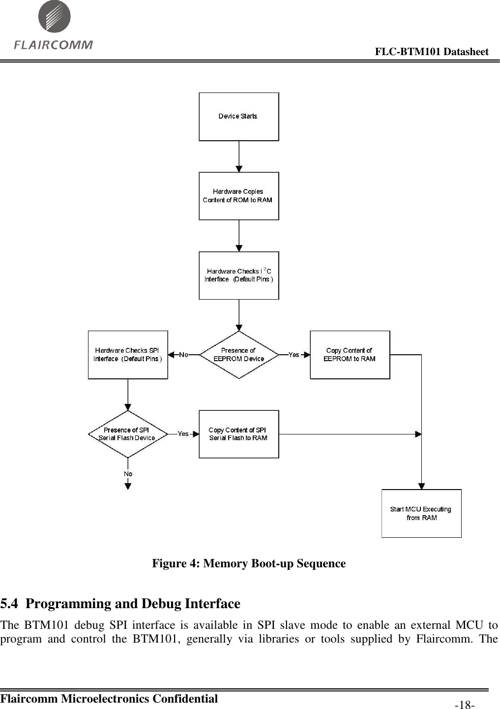
![FLC-BTM101 Datasheet Flaircomm Microelectronics Confidential -19- protocol of this interface is proprietary. The 4 SPI debug lines directly support this function. The SPI programs, configures and debugs the BTM101. Take SPI_PIO#_SEL high to enable the SPI debug feature on PIO [8:5]. BTM101 uses a 16-bit data and 16-bit address programming and debug interface. Transactions occur when the internal processor is running or is stopped. Data is written or read one word at a time, or the auto-increment feature is available for block access. 5.4.1 Instruction Cycle The BTM101 is the slave and receives commands on DEBUG_MOSI and outputs data on DEBUG_MISO. Table 7 shows the instruction cycle for a SPI transaction. 1 Reset the SPI interface Hold DEBUG_CS# high for 2 DEBUG_CLK cycles 2 Write the command word Take DEBUG_CS# low and clock in the 8-bit command 3 Write the address Clock in the 16-bit address word 4 Write or read data words Clock in or out 16-bit data word(s) 5 Termination Take DEBUG_CS# high Table 7: Instruction Cycle for a SPI Transaction With the exception of reset, DEBUG_CS# must be held low during the transaction. Data on DEBUG_MOSI is clocked into the BTM101 on the rising edge of the clock line DEBUG_CLK. When reading, BTM101 replies to the master on DEBUG_MISO with the data changing on the falling edge of the DEBUG_CLK. The master provides the clock on DEBUG_CLK. The transaction is terminated by taking DEBUG_CS# high. The auto increment operation on the BTM101 cuts down on the overhead of sending a command word and the address of a register for each read or write, especially when large amounts of data are to be transferred. The auto increment offers increased data transfer efficiency on the BTM101. To invoke auto increment, DEBUG_CS# is kept low, which auto increments the address, while providing an extra 16 clock cycles for each extra word written or read. 5.4.2 Multi-slave Operation](https://usermanual.wiki/Flaircomm-Microelectronics/BTM101/User-Guide-1783759-Page-19.png)