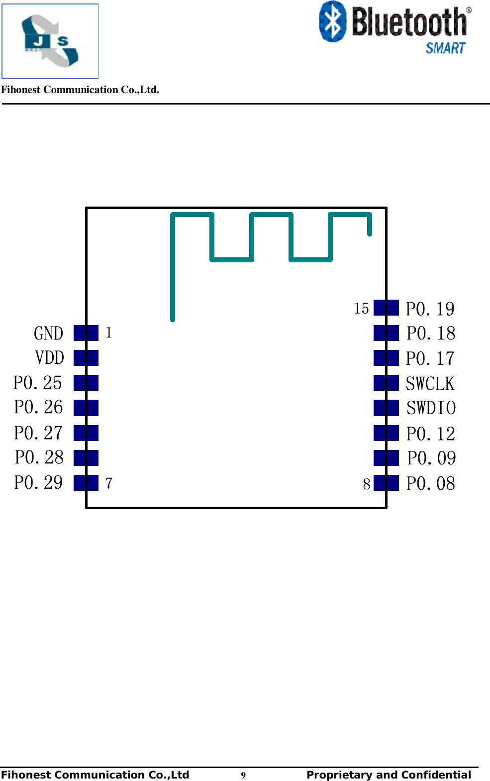
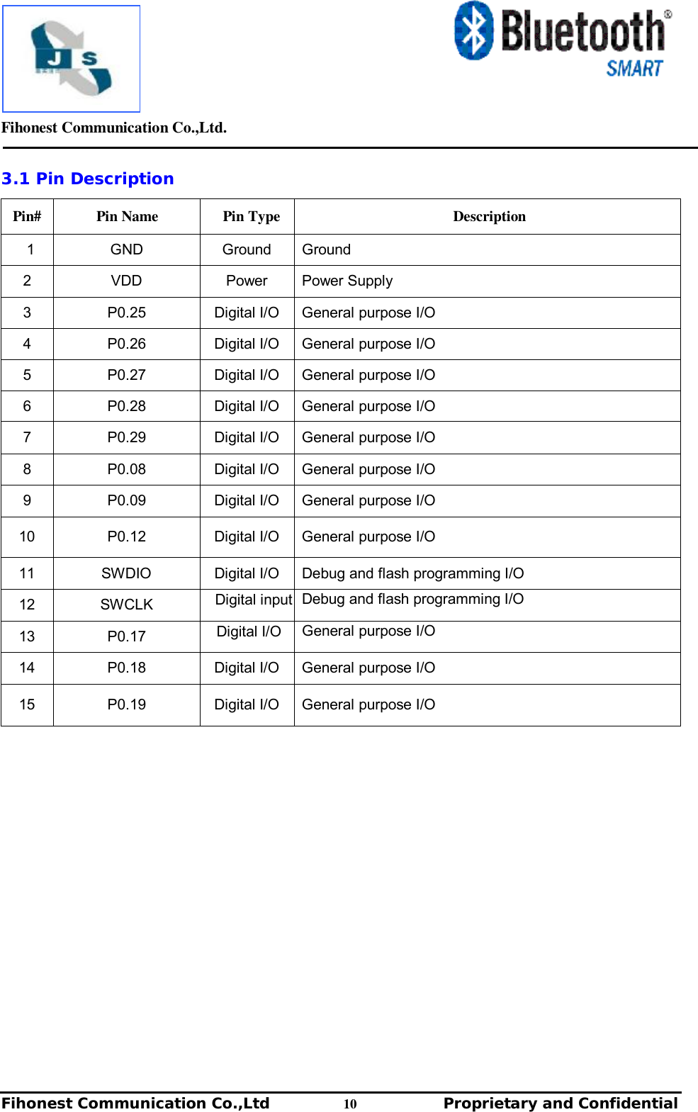
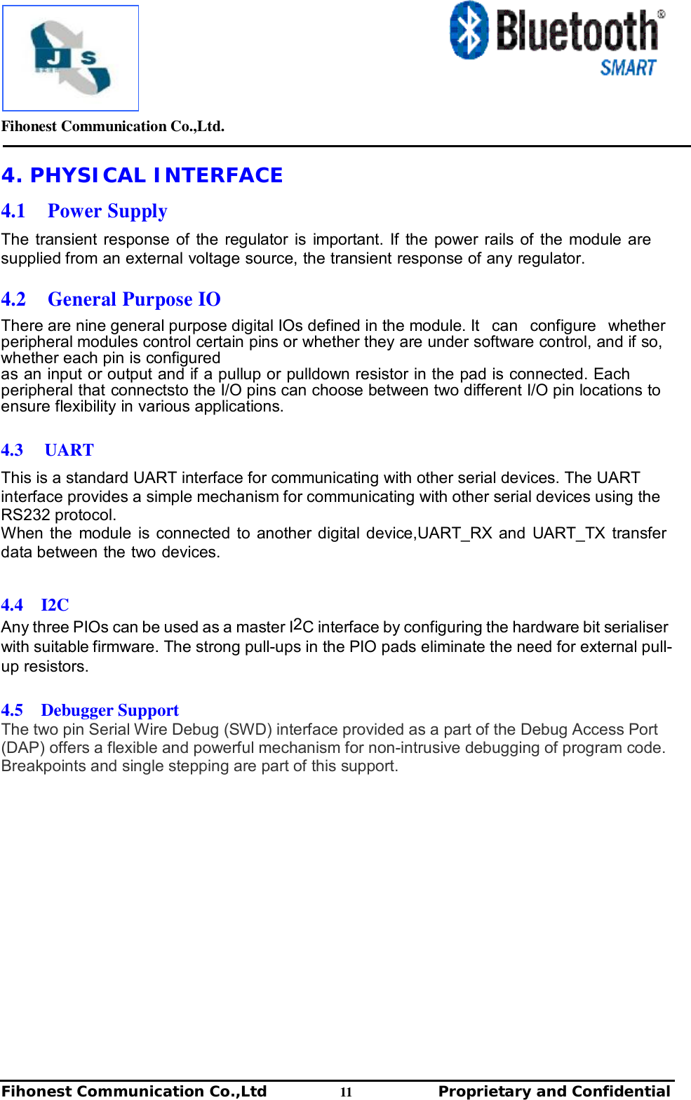
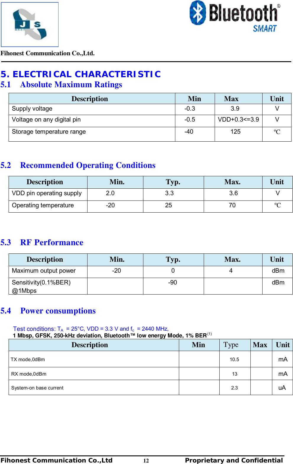
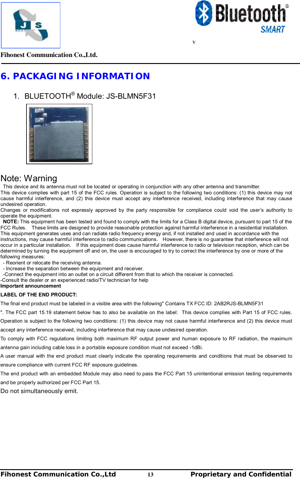
Fihonest Communication JS-BLMN5F31 Bluetooth Module User Manual Fihonest JS BLMN5F31 DATASHEET 201412223

Fihonest Communication Co.,Ltd. Bluetooth Module Fihonest JS BLMN5F31 DATASHEET 201412223

2AB2RJS-BLMN5F31_User Manual REV1

        Fihonest Communication Co.,Ltd.   Fihonest Communication Co.,Ltd          1              Proprietary and Confidential   v       JS-BLMN5F31     Fihonest Bluetooth Module User Manual                       Document Type: Bluetooth Module User Manual  Document Version: V1.0 Release Date: Dec 23, 2014      Copyright 2012 by Fihoenst Communication Co., Ltd. All Rights Reserved.  Reproduction of this document, in part of in whole, by any means is prohibited without written permission from Fihonest Communication Co., Ltd. The information contained herein is believed to be accurate as of the date of publication. However, Fihonest is not liable for any damages, including indirect or consequential from the use of software this document represents, or any reliance of the accuracy of this document. Fihoenst reserves the right to change the contents of this document at any time without notice. This document contains proprietary confidential trade secrets and may be subject to additional restrictions contained in the licensing agreement under which this document was obtained.
        Fihonest Communication Co.,Ltd.   Fihonest Communication Co.,Ltd          2              Proprietary and Confidential   v Revision History  Date  Version Description  Author 2014-12-23  V1.0  n  First Release
        Fihonest Communication Co.,Ltd.   Fihonest Communication Co.,Ltd          3              Proprietary and Confidential   v CONTENT  1.  INTRODUCTION................................................................................................................................. 4  1.1  Block Diagram ........................................................................................................................................ 4 1.2  Features ................................................................................................................................................. 5 1.3  Applications ........................................................................................................................................... 6  2.  GENERAL SPECIFICATION ............................................................................................................ 7   3.  PHYSICAL CHARACTERISTIC...................................................................................................... ..8  3.1  Pin Description.................................................................................................................................... 10  4.   PHYSICAL INTERFACE……………………………………………………………………….…..11  4.1  Power Supply.......................................................................................................................................... .11 4.2  General Purpose I/0............................................................................................................................ 11 4.3  UART.................................................................................................................................................. 11 4.4  I2C....................................................................................................................................................... 11 4.5   Debugger Support............................................................................................................................... ..11  5.  ELECTRICAL CHARACTERISTIC ................................................................................................12  5.1  Absolute Maximus Ratings .......................................................................................................................12 5.2  Recommended Operating Conditions ...........................................................................................................12 5.3   RF Performance……………………………………………………………………………………...12 5.3  Power Consumptions.................................................................................................................................12  6.  PACKAGING INFORMATION ........................................................................................................ 13
        Fihonest Communication Co.,Ltd.   Fihonest Communication Co.,Ltd          4              Proprietary and Confidential   v 1. INTRODUCTION  The JS-BLMN5F31 Bluetooth® module is a perfect solution for bluetooth low energy single mode application. It can be configured,command and contorlled via simple ASCII string with customer application embeded onto the unit. It is slim and light so the designers can have better flexibilities for the bluetooth low energy product shapes.  The JS-BLMN5F31 Bluetooth® module complies with Bluetooth® specification version 4.0(single mode). It includes integrated software stack,profiles,and AT modem like commands.It supports maximum bluetooth data rates via UART interface and provides PIO,I2C,SPI interface for external hardware requirement.  The detail information of JS-BLMN5F31 Bluetooth® module is presented in this document below.    1.1 Block Diagram                                 UART nRF51822 RF match Crystal 16MHz PIO SWD VDD I2C PCB Antenna
        Fihonest Communication Co.,Ltd.   Fihonest Communication Co.,Ltd          5              Proprietary and Confidential   v 1.2 Features ü Small overall dimension ü Bluetooth specification V4.0(single mode) ü Class 2 support  ü -93dBm sensitivity in Bluetooth low energy mode. ü TX Power -20dBm to +4dBm ü ARM Cortex-M0 32 bit processor,256KB Flash memory,16KB RAM n Serial Wire Debug (SWD) ü Complete power-optimized stack,includeing contoller and host ü Embedded bluetooth stack protocols and profiles include: GAP, GATT, SMP, ATT, L2CAP ü Low power consumption (13mA RX, 10.5mA TX, @ 0dBm) ü Ultra low current consumption,flexible power management n 0.4uA @ 3V off mode n 0.5uA @ 3V in off mode + 1 region RAM retention n 2.3uA @ 3V on mode,all blocks IDLE ü Secure and robust communication link with billions of unique codes n FHSS (Frequency Hopping Spread Spectrum) n 24 bit CRC Error correction for guaranteed packet delivery n Lead Free design which is compliant with RoHS requirements ü Flexible real-time counter and two 16 bit and one 24 bit times with counter mode ü AES Coprocessor,random number generator,watchdog timer ü Configurable I/O mapping (I/0 signals can use any pin,simple layout of external application) ü Physical connection as SMD type ※ Some features are optional for customization on demand.
        Fihonest Communication Co.,Ltd.   Fihonest Communication Co.,Ltd          6              Proprietary and Confidential   v 1.3 Application  ü 2.4-GHz Bluetooth low energy Systems  ü Human-interface devices (Keyboard, Mouse,Portable Devices, Remote Control) ü Sports and fitness devices (Heart rate monitor,Foot pod,Cycle speed/power/cadence )  ü Mobile Phone Accessories ü Remote controller via BLE connection ü Health devices (Glucose meter)
        Fihonest Communication Co.,Ltd.   Fihonest Communication Co.,Ltd          7              Proprietary and Confidential   v 2. GENERAL SPECIFICATION General Specification Chip Set  Nordic nRF51822 Module ID  JS-BLMN5F31 BT Standard  Bluetooth® V4.0 specification(single mode) Frequency Band 2.402GHz~2.480GHz ISM Band Modulation  GFSK, 250 KHz deviation Number of channels  40 channels for Bluetooth Low Energy Output Power(Class II)  0±1dBm(L ch), -1±1dBm(M ch),-1±1dBm(H ch)Receive sensitivity  -90dBm @ 0.1% BERBaseband Crystal OSC 32MHz,32.768KHz(optional) RF Input Impedance 50 ohms Host Interface l UART l I2C l PIO  l SWD Temperature  -20ºC to +70ºC
        Fihonest Communication Co.,Ltd.   Fihonest Communication Co.,Ltd          8              Proprietary and Confidential   v 3. PHYSICAL CHARACTERISTIC
        Fihonest Communication Co.,Ltd.   Fihonest Communication Co.,Ltd          9              Proprietary and Confidential   v
        Fihonest Communication Co.,Ltd.   Fihonest Communication Co.,Ltd          10              Proprietary and Confidential   v 3.1 Pin Description  Pin# Pin Name Pin Type Description 1  GND  Ground  Ground 2  VDD  Power  Power Supply 3  P0.25  Digital I/O  General purpose I/O 4  P0.26  Digital I/O  General purpose I/O 5  P0.27  Digital I/O  General purpose I/O 6  P0.28  Digital I/O  General purpose I/O 7  P0.29  Digital I/O  General purpose I/O 8  P0.08  Digital I/O  General purpose I/O 9  P0.09  Digital I/O  General purpose I/O 10  P0.12  Digital I/O  General purpose I/O 11  SWDIO  Digital I/O  Debug and flash programming I/O 12  SWCLK  Digital input Debug and flash programming I/O 13  P0.17  Digital I/O General purpose I/O 14  P0.18  Digital I/O  General purpose I/O 15  P0.19  Digital I/O  General purpose I/O
        Fihonest Communication Co.,Ltd.   Fihonest Communication Co.,Ltd          11              Proprietary and Confidential   v 4. PHYSICAL INTERFACE  4.1  Power Supply  The transient response of the regulator is important. If the power rails of the module are supplied from an external voltage source, the transient response of any regulator.  4.2  General Purpose IO  There are nine general purpose digital IOs defined in the module. It  can  configure  whether  peripheral modules control certain pins or whether they are under software control, and if so, whether each pin is configured as an input or output and if a pullup or pulldown resistor in the pad is connected. Each peripheral that connectsto the I/O pins can choose between two different I/O pin locations to ensure flexibility in various applications.  4.3  UART  This is a standard UART interface for communicating with other serial devices. The UART interface provides a simple mechanism for communicating with other serial devices using the RS232 protocol. When the module is connected to another digital device,UART_RX and UART_TX transfer data between the two devices.  4.4  I2C Any three PIOs can be used as a master I2C interface by configuring the hardware bit serialiser with suitable firmware. The strong pull-ups in the PIO pads eliminate the need for external pull-up resistors.  4.5  Debugger Support The two pin Serial Wire Debug (SWD) interface provided as a part of the Debug Access Port (DAP) offers a flexible and powerful mechanism for non-intrusive debugging of program code. Breakpoints and single stepping are part of this support.
        Fihonest Communication Co.,Ltd.   Fihonest Communication Co.,Ltd          12              Proprietary and Confidential   v 5. ELECTRICAL CHARACTERISTIC 5.1  Absolute Maximum Ratings  Description  Min Max Unit Supply voltage  -0.3  3.9  V Voltage on any digital pin  -0.5  VDD+0.3<=3.9 V Storage temperature range  -40      125  ºC    5.2  Recommended Operating Conditions  Description Min.        Typ. Max. Unit VDD pin operating supply       2.0      3.3       3.6  V Operating temperature       -20      25        70  ºC     5.3  RF Performance  Description Min.        Typ. Max. Unit Maximum output power         -20        0       4  dBm Sensitivity(0.1%BER) @1Mbps                 -90           dBm   5.4  Power consumptions     Test conditions: TA  = 25°C, VDD = 3.3 V and fc  = 2440 MHz,    1 Mbsp, GFSK, 250-kHz deviation, Bluetooth™ low energy Mode, 1% BER (1) Description  Min  Type  Max Unit TX mode,0dBm   10.5  mA RX mode,0dBm  13  mA System-on base current  2.3  uA
        Fihonest Communication Co.,Ltd.   Fihonest Communication Co.,Ltd          13              Proprietary and Confidential   v 6. PACKAGING INFORMATION  1. BLUETOOTH® Module: JS-BLMN5F31            Note: Warning This device and its antenna must not be located or operating in conjunction with any other antenna and transmitter. This device complies with part 15 of the FCC rules. Operation is subject to the following two conditions: (1) this device may not cause harmful interference, and (2) this device must accept any interference received, including interference that may cause undesired operation. Changes or modifications not expressly approved by the party responsible for compliance could void the user’s authority to operate the equipment. NOTE: This equipment has been tested and found to comply with the limits for a Class B digital device, pursuant to part 15 of the FCC Rules.  These limits are designed to provide reasonable protection against harmful interference in a residential installation.  This equipment generates uses and can radiate radio frequency energy and, if not installed and used in accordance with the instructions, may cause harmful interference to radio communications.  However, there is no guarantee that interference will not occur in a particular installation.  If this equipment does cause harmful interference to radio or television reception, which can be determined by turning the equipment off and on, the user is encouraged to try to correct the interference by one or more of the following measures: - Reorient or relocate the receiving antenna. - Increase the separation between the equipment and receiver. -Connect the equipment into an outlet on a circuit different from that to which the receiver is connected. -Consult the dealer or an experienced radio/TV technician for help Important announcement LABEL OF THE END PRODUCT: The final end product must be labeled in a visible area with the following" Contains TX FCC ID: 2AB2RJS-BLMN5F31 ". The FCC part 15.19 statement below has to also be available on the label:  This device complies with Part 15 of FCC rules. Operation is subject to the following two conditions: (1) this device may not cause harmful interference and (2) this device must accept any interference received, including interference that may cause undesired operation. To comply with FCC regulations limiting both maximum RF output power and human exposure to RF radiation, the maximum antenna gain including cable loss in a portable exposure condition must not exceed -1dBi. A user manual with the end product must clearly indicate the operating requirements and conditions that must be observed to ensure compliance with current FCC RF exposure guidelines.  The end product with an embedded Module may also need to pass the FCC Part 15 unintentional emission testing requirements and be properly authorized per FCC Part 15.     Do not simultaneously emit.

Navigation menu