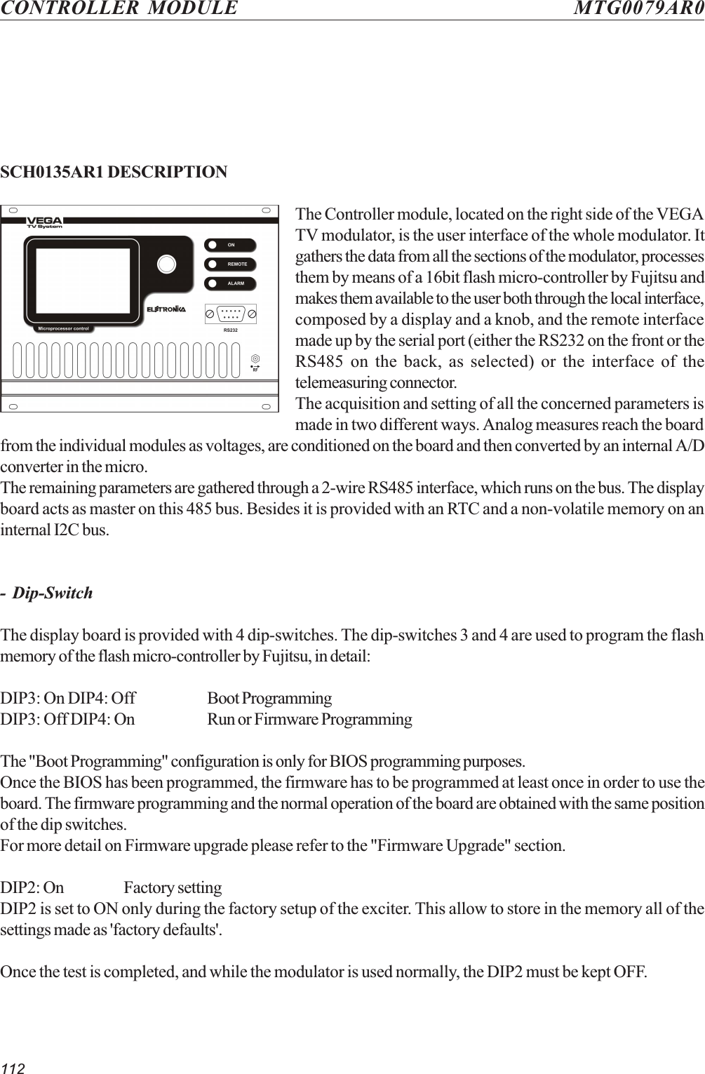
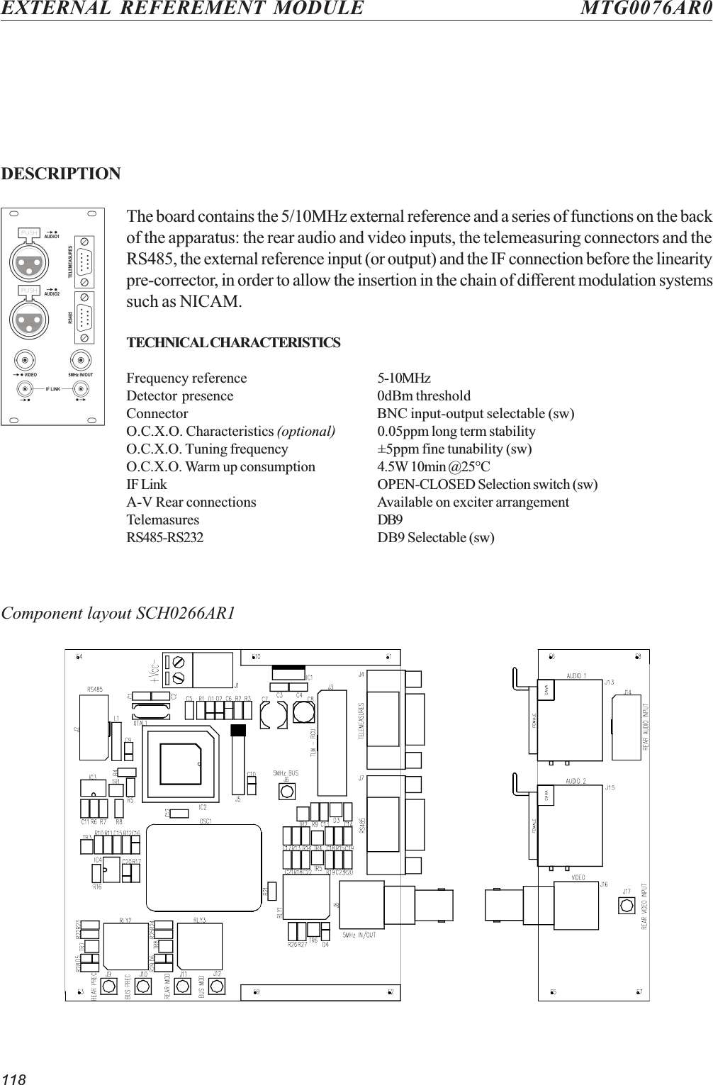
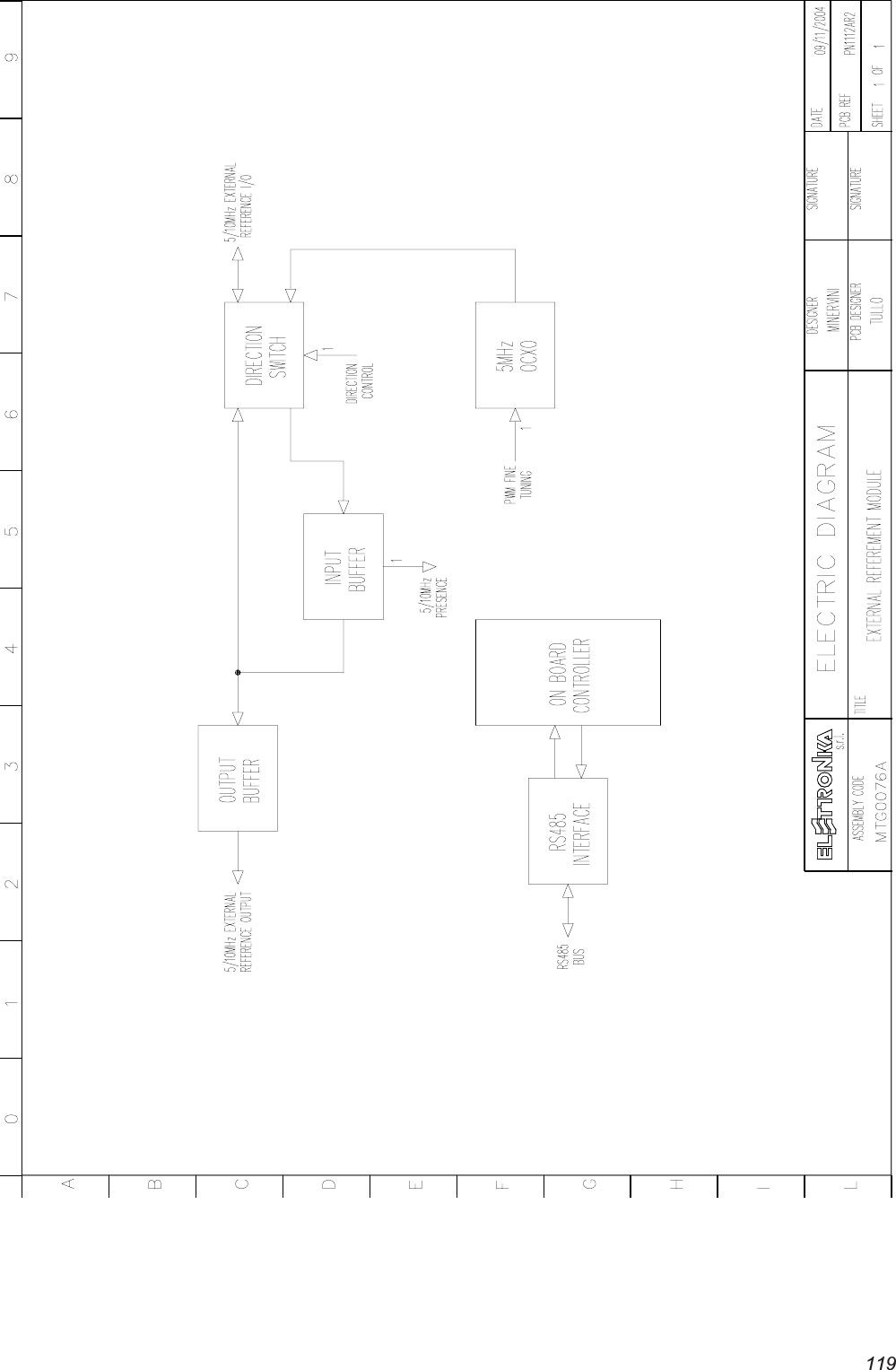
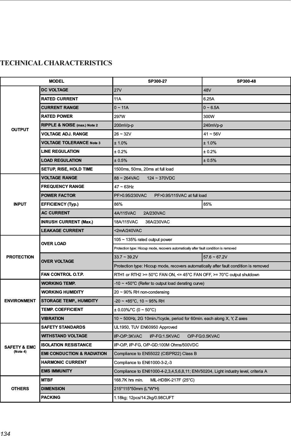
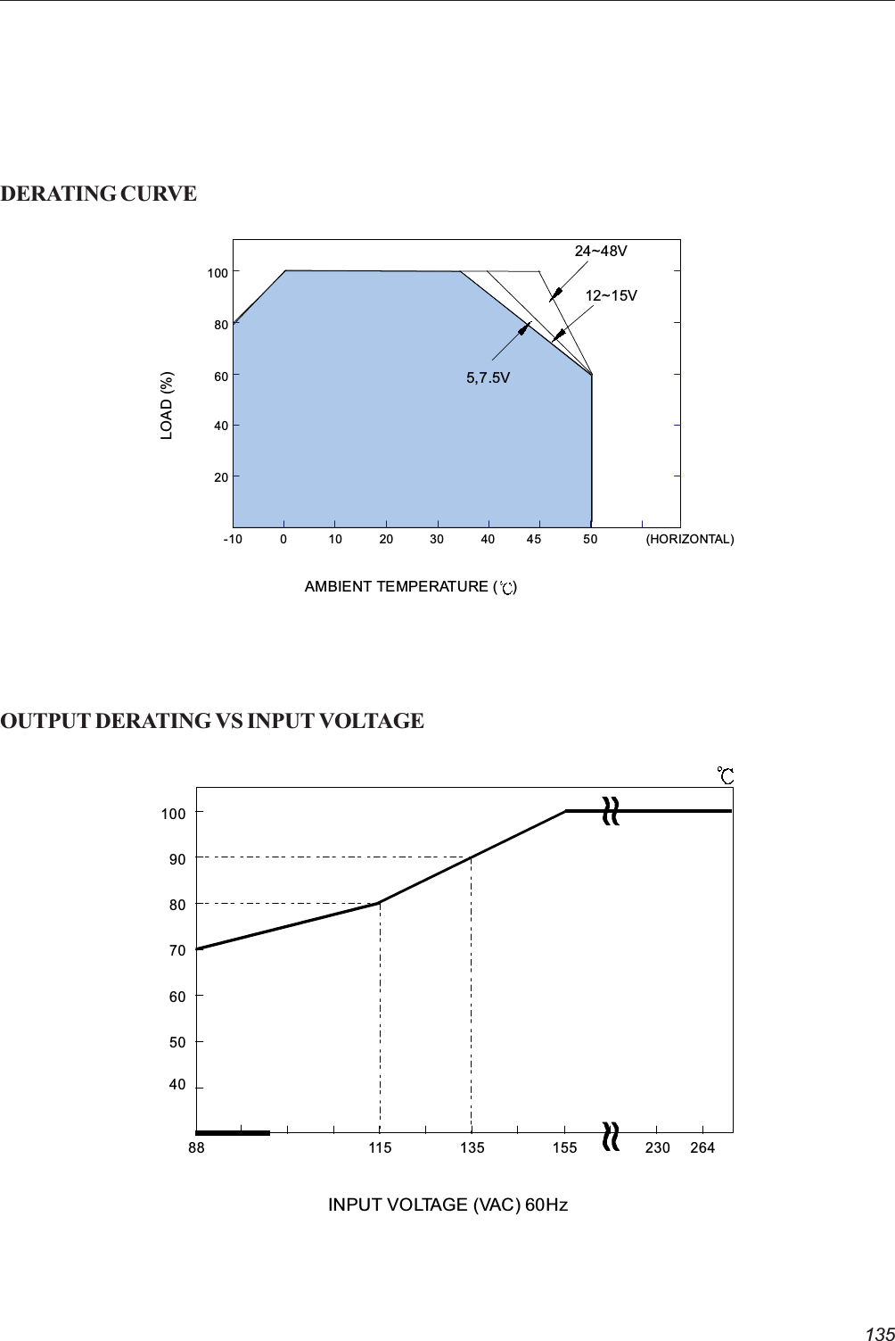
Elettronika S r l TXUP500 500 Watt Analog TV Broadcast Transmitter User Manual APT139B VEGA Rev0 Date100604

Elettronika S.r.l. 500 Watt Analog TV Broadcast Transmitter APT139B VEGA Rev0 Date100604

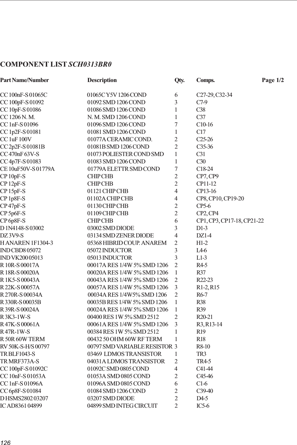
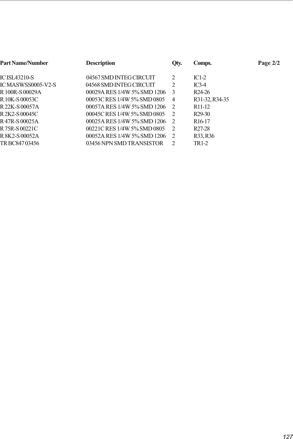
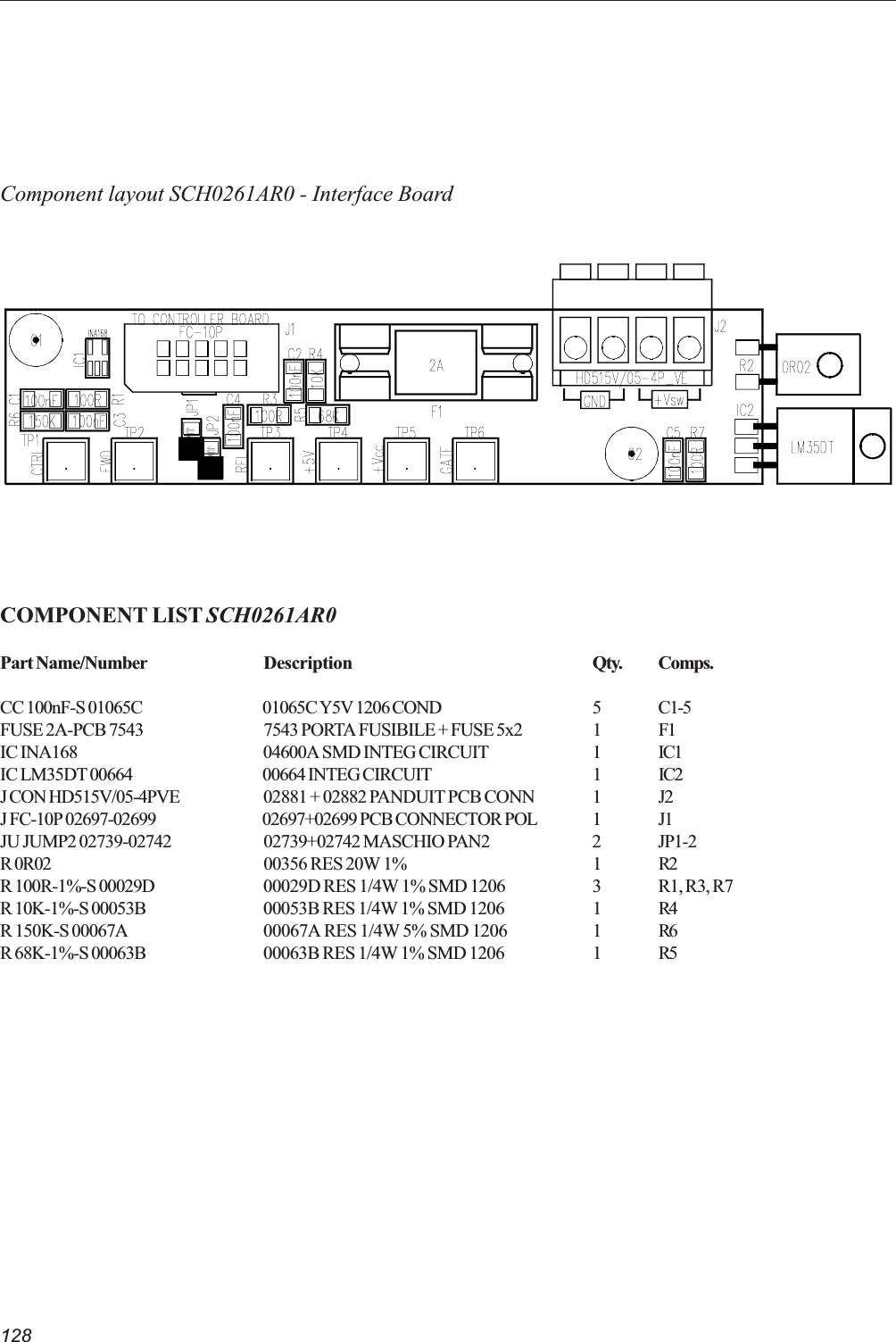
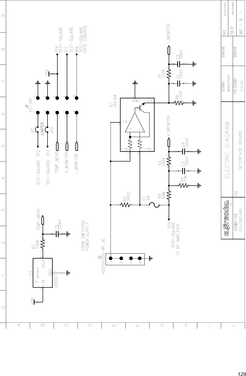
Users manual Exciter Part 3

102MULT. UHF LOCAL OSCILLATOR MODULE MTG0084AR0DESCRIPTIONThe synthesis system of the local oscillator for the channel conversion is based on a controltechnique which allows to obtain the programming of the standard, the channel (split intothe three bands I, III, IV/V) and the line offset (as multiple of the line frequency of thevideo signal) via software, with no change to be made.The module includes an internal VCTCXO reference which can be locked to a moreprecise 5/10MHz reference (trough the bus) needed if the field offset is used.TECHNICAL CHARACTERISTICSNominal level +13dBm  ±1dBFM S/N ccir unweight. > 65dBFM S/N ccir wght. > 60dBAnalog measures VCO control voltageCarrier frequency synthesis A PLLOffset Line offset, step ±1/12 line frequencyO.L. carrier characteristics On/Off selection and fine adjustFrequency reference Internal TCXO externally lockableExternal interface Microprocessor with RS485 protocolFirmware Re-configurable via RS485
103
104The module contains the following blocks:1. Local oscillator  generated the carrier to be synthesised, it is split into three windows (I-II / III / IV-Vband) to ensure the coverage of all of the TV channels to be implemented for all standards.2. Radio-frequency splitter  splits the signal coming from the local oscillator by means of splitters andamplifiers, with 10dB attenuation and gain respectively, to ensure the complete isolation of the LO fromthe other stages and to minimise the frequency pulling phenomenon.3. PLL stage  synthesises the desired channel by locking the LO to a 20MHz frequency reference bymeans of a PLL which can be configured via uWire and provides the locking and line-offset indication(LED on frontal panel); the choice is made via software.4. Active ring filter  stabilises the system in PLL retro-action and e has to be modified if the operatingband of the module changes (see table attached to the electrical diagram).5. Conditioning stage of the correction voltage  conditions the correction voltage of the PLL ringproviding a conditioned analog voltage for the A/D conversion; the voltage is processed by themicrocontroller of the display board (see MTG0079) to be displayed as VU-METER.6. Mixer  in the UPCONVERTER version of the module, converts to channel the intermediate frequencycoming from the pre-corrector (see MTG0073) using a LEVEL13 mixer (in case the module is only usedas LO, see REPEATER configuration, this stage is not present and the synthesised carrier goes directly tothe output of the module).7. 20MHz reference  the frequency reference to the PLL synthesis of the carrier is generated by aninternal TCXO which fine control of the frequency is internally generated via PWM by the microcontrolleror, alternately, can be locked to a more precise 5/10MHz external reference (see MTG0076).8. Controller  all of the described operations are managed by a microcontroller communicating to the userinterface board  (see MTG0079) by RS485 protocol; the local controller stores the status of the moduleand a reprogramming of the firmware (possible via RS485 from the display board) does not alter itscontents.CALIBRATION PROCEDURE- List of instrumentMEASURE INSTRUMENTLock of the carriers and reference- Spectrum analyser- Oscilloscope- Tester
105The calibration procedure of the module requires a complete structure of display board (see MTG0079)and extension module (see MTG0095) in order to perform the software selection which will be referredto later and power the module itself..- Menu of the Multistandard UHF Local Oscillator ModuleVerification of the local oscillator section  connect a spectrum analyser to the monitor of the J4 moduleand check the sections therein:qConfigure the module with Output Enabled, LineOffset Zero, Ref Internal and Channel on thedesired channel, and calibrate C1(C2 and C3) to lock the carrier to the LO frequency of the standard andchannel set (to change the standard refer to the standard changing procedure) and obtain a lockingvoltage between 2V and 3V on TP1, checking that VCO is on Lock in the display menu.Verification of the external reference section  connect a spectrum analyser to the monitor of the J4module and check the sections therein:qConfigure the module with Ref Internal and check that it is possible to find adjust the synthesised frequencyby acting on Tune.- Description of the adjustment pointsCOMPONENT DESCRIPTIONC1, C2, C3 Tuning of the local oscillator (SCH0292 - 0309 - 0310)J3 LO inputJ5, J8 RF link (absent in case of LO configuration)J4 LO monitor (panel)JP1 UnusedJ2 Testpoint for the debug of the PLL
106Component layout for adjustment points
107Component layout SCH0293AR0Component layout SCH0292AR0
108MULT. UHF CHANNEL FILTER MODULE MTG0075AR0DESCRIPTIONThe module filters the signal coming from the conversion mixer removing the local oscillatorand the upper side-band and contains the voltage-controlled gain stage composed by apin-diode attenuation cell followed by a wide-band amplification stage used as driver ofthe final stage.TECHNICAL CHARACTERISTICSInput/output impedance     50W R.O.S.>20dBFilter type      Active 5-cell band-passRF-attenuation type       4 PIN-diodes cellOutput amplifier      Wide bandOverall gain       25dB (max.)The module contains the following blocks:1. Active band-pass filter  filters the lower side-band after conversion, it is split into three windows (I-II/ III / IV-V band)  to ensure the coverage of all of the TV channels to be implemented for all standards,and contains the PIN-diode attenuation cell for the gain control.2. Wide-band amplifier  amplifies the filtered channel in order to obtain the correct driving level for theRF final stages (see MTF0088-0087-0089).CALIBRATION PROCEDURE- List of instrumentsMEASURE INSTRUMENTCalibration of the channel filter - Network analyser- Spectrum analyser with tracking
109The calibration procedure of the module requires a complete structure of display board (see MTG0079)and extension module (see MTG0095) in order to perform the software selection which will be referredto later and power the module itself.- Menu of the Multistandard UHF Channel Filter ModuleVerification of the channel filter  connect a network analyser to the channel filter and calibrate itscomponents to obtain the desired frequency response:qConfigure the module with PwrCtrlMode Man and verify that it is possible to change the gain of the filterby acting on PwrLevelMan, setting JP1 Remote.Verification of the wide-band amplifier section  connect a spectrum analyser with tracking between J4and J5 check that the frequency response of the amplifier is flat within 1dB from 50MHz to 900MHz.- Description of the adjustment pointsCOMPONENT DESCRIPTIONC1-C8, C18-19 Channel filter calibration for bands III and IV-VC17, C20-24,C26-27, C31-32 Channel filter calibration for band I-IIL1-6 Channel filter calibration for band I-IIJ6 RF monitor (panel)JP1, R29 Local gain control of the filterJ2 Channel filter inputJ4 Channel filter output
110Component layout for adjustment points
111Component layout SCH0222AR2Component layout UHF Channel Filter
112CONTROLLER MODULE MTG0079AR0SCH0135AR1 DESCRIPTIONThe Controller module, located on the right side of the VEGATV modulator, is the user interface of the whole modulator. Itgathers the data from all the sections of the modulator, processesthem by means of a 16bit flash micro-controller by Fujitsu andmakes them available to the user both through the local interface,composed by a display and a knob, and the remote interfacemade up by the serial port (either the RS232 on the front or theRS485 on the back, as selected) or the interface of thetelemeasuring connector.The acquisition and setting of all the concerned parameters ismade in two different ways. Analog measures reach the boardfrom the individual modules as voltages, are conditioned on the board and then converted by an internal A/Dconverter in the micro.The remaining parameters are gathered through a 2-wire RS485 interface, which runs on the bus. The displayboard acts as master on this 485 bus. Besides it is provided with an RTC and a non-volatile memory on aninternal I2C bus.- Dip-SwitchThe display board is provided with 4 dip-switches. The dip-switches 3 and 4 are used to program the flashmemory of the flash micro-controller by Fujitsu, in detail:DIP3: On DIP4: Off Boot ProgrammingDIP3: Off DIP4: On Run or Firmware ProgrammingThe "Boot Programming" configuration is only for BIOS programming purposes.Once the BIOS has been programmed, the firmware has to be programmed at least once in order to use theboard. The firmware programming and the normal operation of the board are obtained with the same positionof the dip switches.For more detail on Firmware upgrade please refer to the "Firmware Upgrade" section.DIP2: On Factory settingDIP2 is set to ON only during the factory setup of the exciter. This allow to store in the memory all of thesettings made as 'factory defaults'.Once the test is completed, and while the modulator is used normally, the DIP2 must be kept OFF.
113- LEDsThe board is provided with three LEDs.- On (green): it is lit when the exciter is switched on by local or remote control. The LED is blinking till thepower reach his nominal value.- Remote (yellow): it is lit when the exciter has been set to accept remote commands. To have it accept localcommands again, the local/remote selection menu can be used.- Alarm (red): shows that an alarm is present.In case of alarm the red LED lights up and the icon of a bell appears in the upper bar of the display. If the alarmdisappears, the red LED is turned off and the bell starts blinking, in order to show that an anomaly occurred.To know the details of the anomaly and when it occurred, the history menu can be used. Once this menu isaccessed, the blinking bell icon disappears.While an alarm is present the exciter switch off the output power. When the alarm disappear, the power isswitched on again. After 5 times the exciter switch off the output power, the exciter goes in LockOut state: thepower remains off till the user reset the LockOut. If the fails are far more that 1 hour than the LockOut counteris automatically cleaned.TECHNICAL CHARACTERISTICSFlash ROM 256kByteRAM 6kByteEEPROM 64kBitSerial interfaces 2xRS485 or 1xRS485 + 1xRS232Graphic display 128x64pixel blue with white LED back lightEncoder Mechanical with push buttonClock and Calendar Lithium battery backupTelemeasures Output: FWD, REF, AlarmInput: Remote OFFFIRMWARE UPGRADEInside the VEGA exciter there are 5 micro-controllers. One of these is the one of the display board (16bitFujitsu with 256K Flash) while 4 are in the audio, video, local oscillator and external reference boardsrespectively (8bit Microchip with 8K Flash).It is possible to upgrade all of the micro-controllers of the exciter, but the procedures differ from the displayone and the remaining four.All upgrades are made by means of the RS232 connector on the front panel of the exciter.All of the firmware inside the exciter are made up by two parts: the BIOS and the firmware proper. Theformer only programs the built-in Flash memory, while all of the operations of the micro are determined by the
114latter.l Upgrade of the BIOS of the display board:While the exciter is off, set the dip-switched of the board on these positions DIP3:ON DIP4:OFF. Run theFujitsu Flash MCU programmer application, select the BIOS file to be used, select download and follow theinstructions given by the application.l     Upgrade of the FIRMWARE  of the display board:A display board provided with the BIOS is needed.While the exciter is off, set the dip-switched of the board on these positions DIP3:OFF DIP4:ON. Run theVega Flash Application, select the upgrade of the display board and the file to be used, select download andswitch the exciter on. The upgrade will start automatically.l     Upgrade of the boards on the BUS:A working display board is needed in order to upgrade the boards on the BUS, because the programming ofthe modules is made trough the display board.Warning: while it is possible to program both the BIOS and the firmware of the display board, it is onlypossible to change the firmware, and not the BIOS, of the boards on the bus. Since the BIOS is in the samemicro as the firmware, this means that it is not possible to program the micro of a board on the bus on  a virginmicro, which can be done, instead, on the display.To proceed with the upgrade, while the exciter is on and remote, run the Vega Flash Application, select theboard to be upgraded and the file to be sent, then select download. The upgrade will start automatically.
115
116Component layout SCH0135AR1 - Bot layerComponent layout SCH0135AR1 - Top layer
117Component layout SCH0231AR1SCH0231AR1 DESCRIPTIONThe power supply accepts a nominal continuous input voltage of 28V and supplies three continuous currentoutput with voltages of +5V, +15V and -15V. It also provides a voltage of +28V to the system bus. Thepower supply voltages towards the system bus are switched by means of relays controlled by the micro-processor of the control board.There are switching regulators for the +5V, +15V and -15V voltages.The power supply board provides the operating voltages to the control board trough multi-wire flat cable. Inthis there are also analog voltages to monitor the power supply status. The monitoring of the +5V, +15V and-15V voltages are conditioned to about 4V nominal.The board provides the power supply to the system fan. Its on/off status and its speed can be set by themicro-processor of the control board.The connections to the system bus and power supply board are made using a fast-lock connector.
118EXTERNAL REFEREMENT MODULE MTG0076AR0DESCRIPTIONThe board contains the 5/10MHz external reference and a series of functions on the backof the apparatus: the rear audio and video inputs, the telemeasuring connectors and theRS485, the external reference input (or output) and the IF connection before the linearitypre-corrector, in order to allow the insertion in the chain of different modulation systemssuch as NICAM.TECHNICAL CHARACTERISTICSFrequency reference 5-10MHzDetector presence 0dBm thresholdConnector BNC input-output selectable (sw)O.C.X.O. Characteristics (optional) 0.05ppm long term stabilityO.C.X.O. Tuning frequency ±5ppm fine tunability (sw)O.C.X.O. Warm up consumption 4.5W 10min @25°CIF Link OPEN-CLOSED Selection switch (sw)A-V Rear connections Available on exciter arrangementTelemasures DB9RS485-RS232 DB9 Selectable (sw)Component layout SCH0266AR1
119
120The module contains the following blocks:1. Input and output buffers  de-couple the internal circuitry from the I/O conenctors and detect thepresence of the reference signal.2. Direction switch  allows the configuration of the BNC as either input or output for the 5/10MHzreference signal.3. 5MHz O.C.X.O. 5MHz internal reference system (optional), which frequency can be fine-adjustedvia software.4. Controller  all of the described operations are managed by a microcontroller communicating to the userinterface board (see MTG0079) by RS485 protocol; the local controller stores the status of the moduleand a reprogramming of the firmware (possible via RS485 from the display board) does not after itscontents.EXTERNAL PIN OUT CONNECTORSTelemeasures (DB9)     RS485 (DB9)CALIBRATION PROCEDURE- List of instrumentPIN N° SIGNAL TYPE IN / OUT FUNCTION1Analog Output FWD Power2Analog Output REF Power3 Analog Output Temperature4 Analog Input FWD Power5GND - -6 Digital Output Free contact with pin7 - Alarm7 Digital Output Free contact with pin6 - Alarm8 Digital Input GND= Off  -  OPEN= On9 Digital Input N.U.PIN N° FUNCTION1N.C.2RX-3RX+4+5V5GND6+5V7TX-8TX+9N.C.MEASURE INSTRUMENTFrequency referement control - Spectrum analyser
121The calibration procedure of the module requires a complete structure of display board (see MTG0079)in order to perform the software selection which will be referred to later and power the module itself..- Menu of the External Referement ModuleVerification of the external reference section  connect a spectrum analyser to the BNC labelled EXTREF IN/OUT and check the sections therein:qConfigure the module with ExtREF Dir Out and check the presence of the 5MHz carrier withExtReference set to Pres in the display menu.qCheck that the 5MHz frequency is fine-adjusted by acting on ExtRef Tune.Verification of the IF Link section:qConfigure the module with IF Link open and closed checking the switching of the relays.
12215W UHF AMPLIFIER MODULE MTF0088BR0Component layout MTF0088BR0
123Component layout SCH0313BR0 - 15W UHF Amplifier Module
124
125
126COMPONENT LIST SCH0313BR0Part Name/Number Description Qty. Comps. Page 1/2CC 100nF-S 01065C 01065C Y5V 1206 COND 6 C27-29, C32-34CC 100pF-S 01092 01092 SMD 1206 COND 3 C7-9CC 10pF-S 01086 01086 SMD 1206 COND 1 C38CC 1206 N. M. N. M. SMD 1206 COND 1 C37CC 1nF-S 01096 01096 SMD 1206 COND 7 C10-16CC 1p2F-S 01081 01081 SMD 1206 COND 1 C17CC 1uF 100V 01077A CERAMIC COND. 2 C25-26CC 2p2F-S 01081B 01081B SMD 1206 COND 2 C35-36CC 470nF 63V-S 01073 POLIESTER COND SMD 1 C31CC 4p7F-S 01083 01083 SMD 1206 COND 1 C30CE 10uF50V-S 01779A 01779A ELETTR SMD COND 7 C18-24CP 10pF-S CHIP CHB 2 CP7, CP9CP 12pF-S CHIP CHB 2 CP11-12CP 15pF-S 01121 CHIP CHB 4 CP13-16CP 1p8F-S 01102A CHIP CHB 4 CP8, CP10, CP19-20CP 47pF-S 01130 CHIP CHB 2 CP5-6CP 5p6F-S 01109 CHIP CHB 2 CP2, CP4CP 6p8F-S CHIP CHB 6 CP1, CP3, CP17-18, CP21-22D 1N4148-S 03002 03002 SMD DIODE 3 D1-3DZ 3V9-S 03134 SMD ZENER DIODE 4 DZ1-4H ANAREN 1F1304-3 05368 HIBRID COUP. ANAREM 2 H1-2IND CBD8 05072 05072 INDUCTOR 3 L4-6IND VK200 05013 05013 INDUCTOR 3 L1-3R 10R-S 00017A 00017A RES 1/4W 5% SMD 1206 2 R4-5R 18R-S 00020A 00020A RES 1/4W 5% SMD 1206 1 R37R 1K5-S 00043A 00043A RES 1/4W 5% SMD 1206 2 R22-23R 22K-S 00057A 00057A RES 1/4W 5% SMD 1206 3 R1-2, R15R 270R-S 00034A 00034A RES 1/4W5% SMD 1206 2 R6-7R 330R-S 00035B 00035B RES 1/4W 5% SMD 1206 1 R38R 39R-S 00024A 00024A RES 1/4W 5% SMD 1206 1 R39R 3K3-1W-S 00400 RES 1W 5% SMD 2512 2 R20-21R 47K-S 00061A 00061A RES 1/4W 5% SMD 1206 3 R3, R13-14R 47R-1W-S 00384 RES 1W 5% SMD 2512 1 R19R 50R 60W TERM 00432 50 OHM 60W RF TERM 1 R18RV 50K-S-H/S 00797 00797 SMD VARIABLE RESISTOR 3 R8-10TR BLF1043-S 03469  LDMOS TRANSISTOR 1 TR3TR MRF373A-S 04031A LDMOS TRANSISTOR 2 TR4-5CC 100pF-S 01092C 01092C SMD 0805 COND 4 C41-44CC 10nF-S 01053A 01053A SMD 0805 COND 2 C45-46CC 1nF-S 01096A 01096A SMD 0805 COND 6 C1-6CC 6p8F-S 01084 01084 SMD 1206 COND 2 C39-40D HSMS2802 03207 03207 SMD DIODE 2 D4-5IC AD8361 04899 04899 SMD INTEG CIRCUIT 2 IC5-6
127Part Name/Number Description Qty. Comps. Page 2/2IC ISL43210-S 04567 SMD INTEG CIRCUIT 2 IC1-2IC MASWSS0005-V2-S 04568 SMD INTEG CIRCUIT 2 IC3-4R 100R-S 00029A 00029A RES 1/4W 5% SMD 1206 3 R24-26R 10K-S 00053C 00053C RES 1/4W 5% SMD 0805 4 R31-32, R34-35R 22K-S 00057A 00057A RES 1/4W 5% SMD 1206 2 R11-12R 2K2-S 00045C 00045C RES 1/4W 5% SMD 0805 2 R29-30R 47R-S 00025A 00025A RES 1/4W 5% SMD 1206 2 R16-17R 75R-S 00221C 00221C RES 1/4W 5% SMD 0805 2 R27-28R 8K2-S 00052A 00052A RES 1/4W 5% SMD 1206 2 R33, R36TR BC847 03456 03456 NPN SMD TRANSISTOR 2 TR1-2
128Component layout SCH0261AR0 - Interface BoardCOMPONENT LIST SCH0261AR0Part Name/Number Description Qty. Comps.CC 100nF-S 01065C 01065C Y5V 1206 COND 5 C1-5FUSE 2A-PCB 7543 7543 PORTA FUSIBILE + FUSE 5x2 1 F1IC INA168 04600A SMD INTEG CIRCUIT 1 IC1IC LM35DT 00664 00664 INTEG CIRCUIT 1 IC2J CON HD515V/05-4PVE 02881 + 02882 PANDUIT PCB CONN 1 J2J FC-10P 02697-02699 02697+02699 PCB CONNECTOR POL 1 J1JU JUMP2 02739-02742 02739+02742 MASCHIO PAN2 2 JP1-2R 0R02 00356 RES 20W 1% 1 R2R 100R-1%-S 00029D 00029D RES 1/4W 1% SMD 1206 3 R1, R3, R7R 10K-1%-S 00053B 00053B RES 1/4W 1% SMD 1206 1 R4R 150K-S 00067A 00067A RES 1/4W 5% SMD 1206 1 R6R 68K-1%-S 00063B 00063B RES 1/4W 1% SMD 1206 1 R5
129
130Component layout SCH0194AR1BUS STRUCTURE SCH0194AR1
131
132COMPONENT LIST SCH0194AR1Part Name/Number Description Qty. Comps.CC 100nF-S 01065C 01065C Y5V 1206 COND 19 C1-2, C4, C7-8, C10-12, C15-18,C23, C25-28, C31-32CC 10nF-S 01053B 01053B SMD 1206 COND 2 C14, C22CC 1206 N. M. N. M. SMD 1206 COND 2 C13, C24CC 47pF-S 01100 01100 SMD 1206 COND 1 C21CE 220uF50V LOW ESR 01799A ELETTR SMD COND LOW ESR 8 C3, C5-6, C9, C19-20, C29-30D 1N4148-S 03002 03002 SMD DIODE 2 D3, D5D 50WQ06FN 03019A SMD DIODE SCHOTTKY 5,5A 5 D1-2, D4, D6-7DL KA-3528SGC 03057 03057 GREEN SMD LED DIODE 4 DL1-4IC LM2593HVS-ADJ 04089 SMD INTEG CIRCUIT 2 IC3, IC8IC LM2596S-5.0 04580 SMD INTEG CIRCUIT 1 IC2IC LM317 04340 04340 INTEG CIRCUIT 1 IC1IC TL082-S 04796A 04796A SMD INTEG CIRCUIT 2 IC5, IC7IC TPS2034D-S 04088 SMD INTEG CIRCUIT 1 IC6IC ULN2003A 4870 04870 SMD INTEG CIRCUIT 1 IC4IND MS85 10uH-S 04948 INDUCTOR 2,7A 3 L1, L3, L6IND T100uH-1.8A 4958 04958 TOROIDAL-STORAGE CHOKES 3 L2, L4-5J CON HD515V/05-4PVE 02881 + 02882 PANDUIT PCB CONN 1 J1J CON HD515V/05-6PVE 02883 + 02884 PANDUIT PCB CONN 1 J2J FC-16P 02701-02700 02701+02700 PCB CONNECTOR POL 1 J3R 100K-1%-S 00065B 00065B RES 1/4W 1% SMD 1206 2 R18, R20R 100R-1%-S 00029D 00029D RES 1/4W 1% SMD 1206 3 R14-15, R25R 10K-1%-S 00053B 00053B RES 1/4W 1% SMD 1206 4 R3, R7, R19, R26R 10R-1%-S 00017D 00017D RES 1/4W 1% SMD 1206 4 R13, R17, R28-29R 12K-1%-S 00054B 00054B RES 1/4W 1% SMD 1206 1 R10R 1K0-1%-S 00041B 00041B RES 1/4W 1% SMD 1206 2 R5, R30R 1K2-1%-S 00042A 00042A RES 1/4W 1% SMD 1206 4 R6, R8, R23, R27R 220R-1%-S 00033C 00033C RES 1/4W 1% SMD 1206 1 R1R 22K-1%-S 00057B 00057B RES 1/4W 1% SMD 1206 2 R9, R16R 27K-1%-S 00058B 00058B RES 1/4W 1% SMD 1206 1 R22R 2K2-1%-S 00045B 00045B RES 1/4W 1% SMD 1206 1 R12R 330R-1%-S 00035A 00035A RES 1/4W 1% SMD 1206 1 R4R 33K-1%-S 00059B 00059B RES 1/4W 1% SMD 1206 2 R11, R21R 68K-1%-S 00063B 00063B RES 1/4W 1% SMD 1206 1 R24R 6K8-1%-S 00051B 00051B RES 1/4W 1% SMD 1206 1 R2RL 30.22.24 07569 07569 RELE 2 RLY1-2TR BC856 03455 03455 PNP SMD TRANSISTOR 1 TR1
133SP300-27 SWITCHING POWER SUPPLY E0017MAIN FEATURES- Universal AC input / Full range- Built-in active PFC function, PF>0.95- Protections: Short circuit / Over load / Over voltage / Over temp.- Forced air cooling by built-in DC fan- Built-in cooling Fan ON-OFF control- Fixed switching frequency at 110kHzMECHANICAL SPECIFICATIONAir flowdirection21532.550254-M4 L=6mm150CLPIN N° ASSIGNMENT1AC/L2AC/N3FG4-5 DC OUTPUT -V6-7 DC OUTPUT +V
134TECHNICAL CHARACTERISTICSMODEL SP300-27 SP300-48OUTPUTDC VOLTAGE 27V 48VRATED CURRENT 11A 6.25ACURRENT RANGE 0 ~ 11A 0 ~ 6.5ARATED POWER 297W 300WRIPPLE & NOISE (max.) Note 2 200mVp-p 240mVp-pVOLTAGE ADJ. RANGE 26 ~ 32V 41 ~ 56VVOLTAGE TOLERANCE Note 3 ± 1.0% ± 1.0%LINE REGULATION ± 0.2% ± 0.2%LOAD REGULATION ± 0.5% ± 0.5%SETUP, RISE, HOLD TIME 1500ms, 50ms, 20ms at full loadINPUTVOLTAGE RANGE 88 ~ 264VAC      124 ~ 370VDCFREQUENCY RANGE 47 ~ 63HzPOWER FACTOR PF>0.95/230VAC      PF>0.95/115VAC at full loadEFFICIENCY (Typ.) 86% 85%AC CURRENT 4A/115VAC      2A/230VACINRUSH CURRENT (Max.) 18A/115VAC      36A/230VACLEAKAGE CURRENT <2mA/240VACPROTECTIONOVER LOAD105 ~ 135% rated output powerProtection type: Hiccup mode, recovers automatically after fault condition is removedOVER VOLTAGE33.7 ~ 39.2V 57.6 ~ 67.2VProtection type: Hiccup mode, recovers automatically after fault condition is removedFAN CONTROL O.T.P. RTH1 or RTH2 >= 50°C FAN ON, <= 45°C FAN OFF, >= 70°C output shutdownENVIRONMENTWORKING TEMP. -10 ~ +50°C (Refer to output load derating curve)WORKING HUMIDITY 20 ~ 90% RH non-condensingSTORAGE TEMP., HUMIDITY -20 ~ +85°C, 10 ~ 95% RHTEMP. COEFFICIENT ± 0.03%/°C (0 ~ 50°C)VIBRATION 10 ~ 500Hz, 2G 10min./1cycle, period for 60min. each along X, Y, Z axesSAFETY & EMC(Note 4)SAFETY STANDARDS UL1950, TUV EN60950 ApprovedWITHSTAND VOLTAGE I/P-O/P:3KVAC      I/P-FG:1.5KVAC      O/P-FG:0.5KVACISOLATION RESISTANCE I/P-O/P, I/P-FG, O/P-GD:100M Ohms/500VDCEMI CONDUCTION & RADIATION Compliance to EN55022 (CISPR22) Class BHARMONIC CURRENT Compliance to EN61000-3-2,-3EMS IMMUNITY Compliance to EN61000-4-2,3,4,5,6,8,11; ENV50204, Light industry level, criteria AOTHERSMTBF 168.7K hrs min.      MIL-HDBK-217F (25°C)DIMENSION 215*115*50mm (L*W*H)PACKING 1.18kg; 12pcs/14.2kg/0.98CUFT
135DERATING CURVEOUTPUT DERATING VS INPUT VOLTAGEAMBIENT TEMPERATURE ( )LOAD (%)20406080100-10 0 10 20 30 40 45 50 (HORIZONTAL)12~15V5,7.5V24~48VINPUT VOLTAGE (VAC) 60Hz88 115 135 155 264230901008070605040

Navigation menu