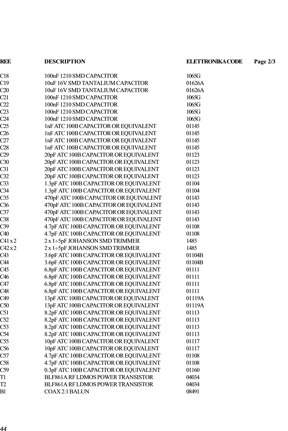
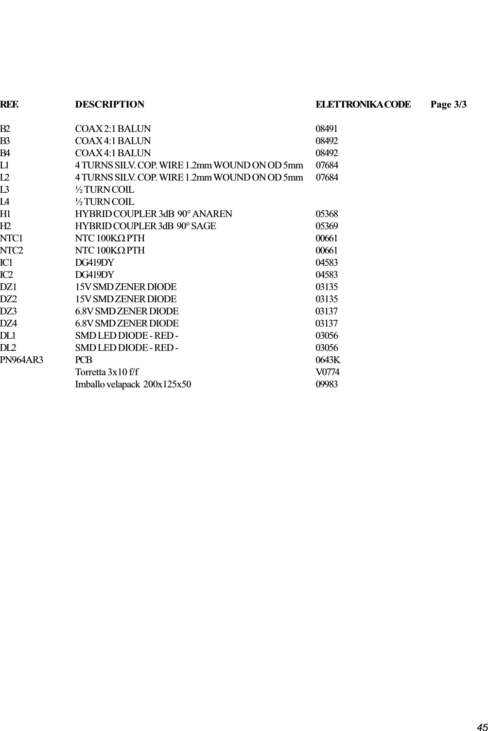
Elettronika S r l TXUP1000 1000 Watt Analog TV Broadcast Transmitter User Manual APT148B AUTV 1000LD Rev0 Date040305p65 p65
Elettronika S.r.l. 1000 Watt Analog TV Broadcast Transmitter APT148B AUTV 1000LD Rev0 Date040305p65 p65
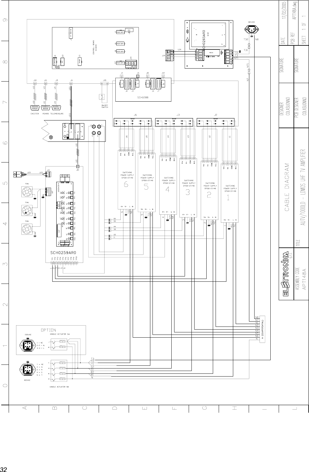
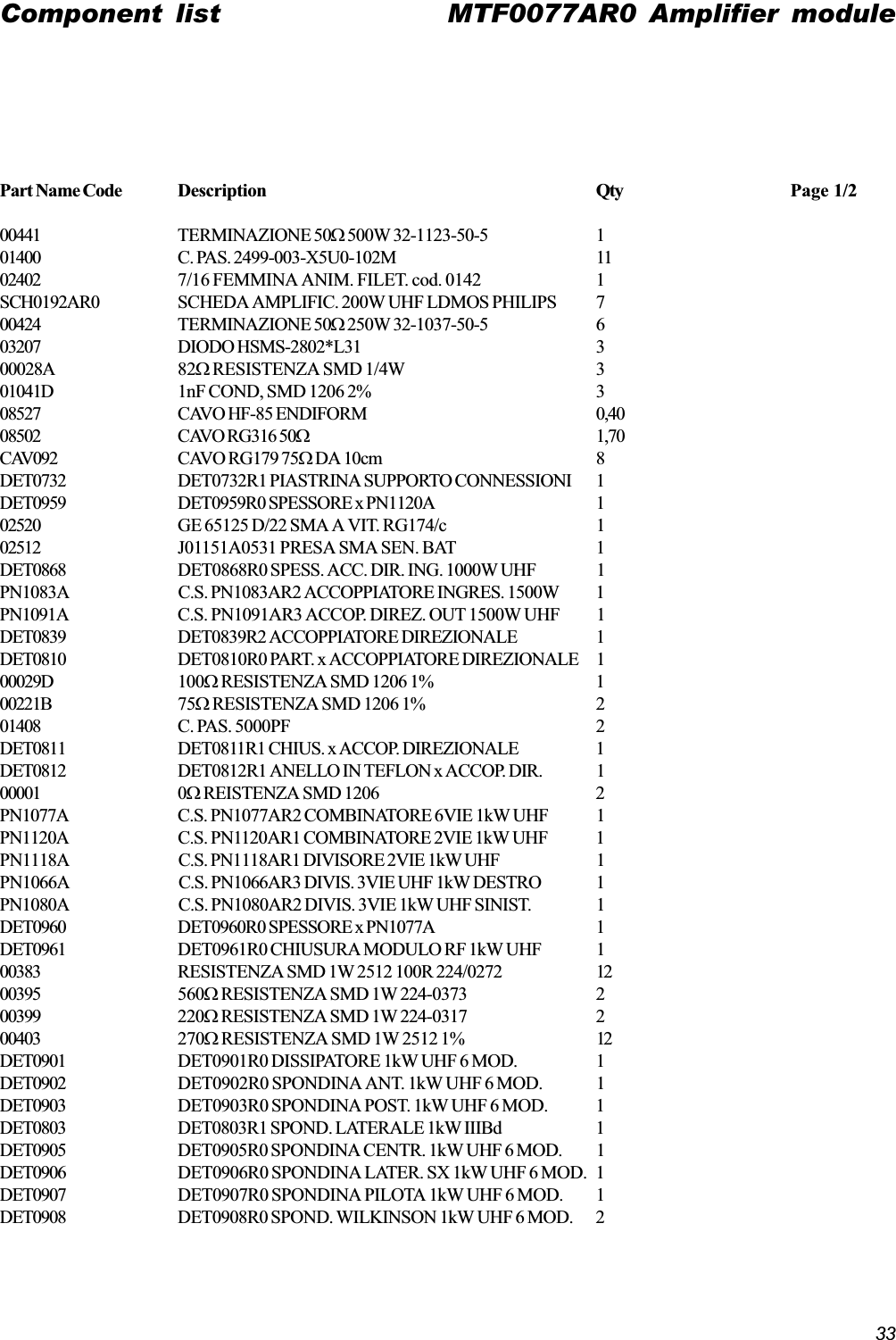
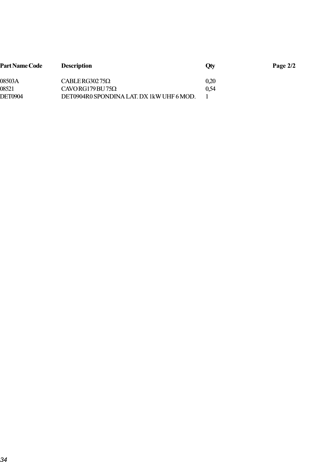
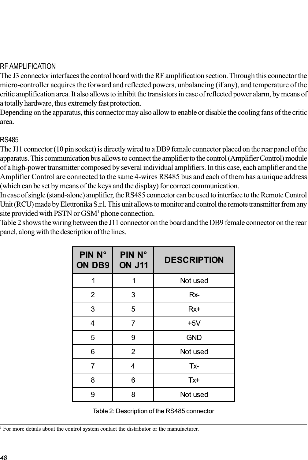
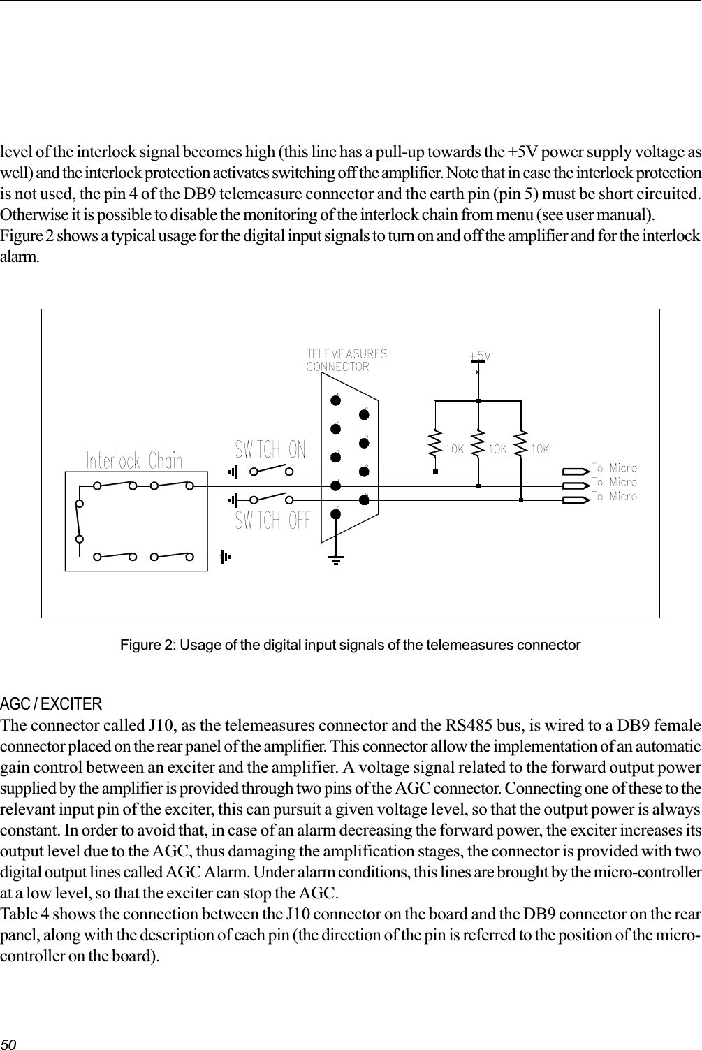
Contents
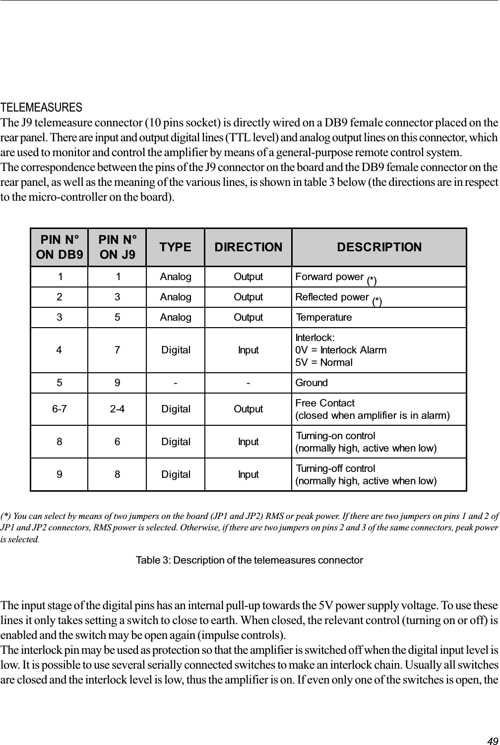
- 1. Exciter User Manual Part 1
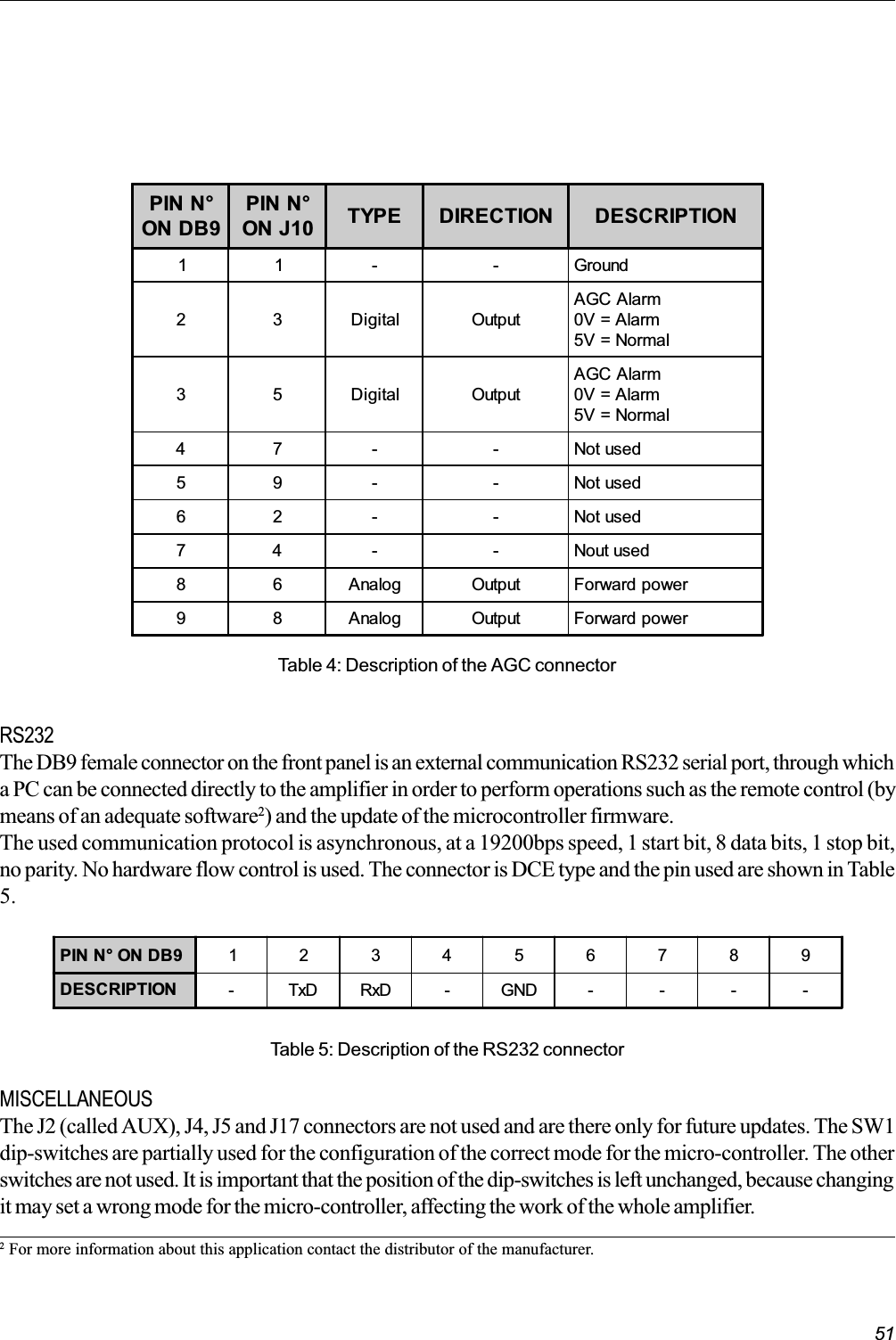
- 2. Exciter User Manual Part 2
- 3. Exciter User Manual Part 3
- 4. Amplifier User manual Part 1
- 5. Amplifier User Manual Part 2
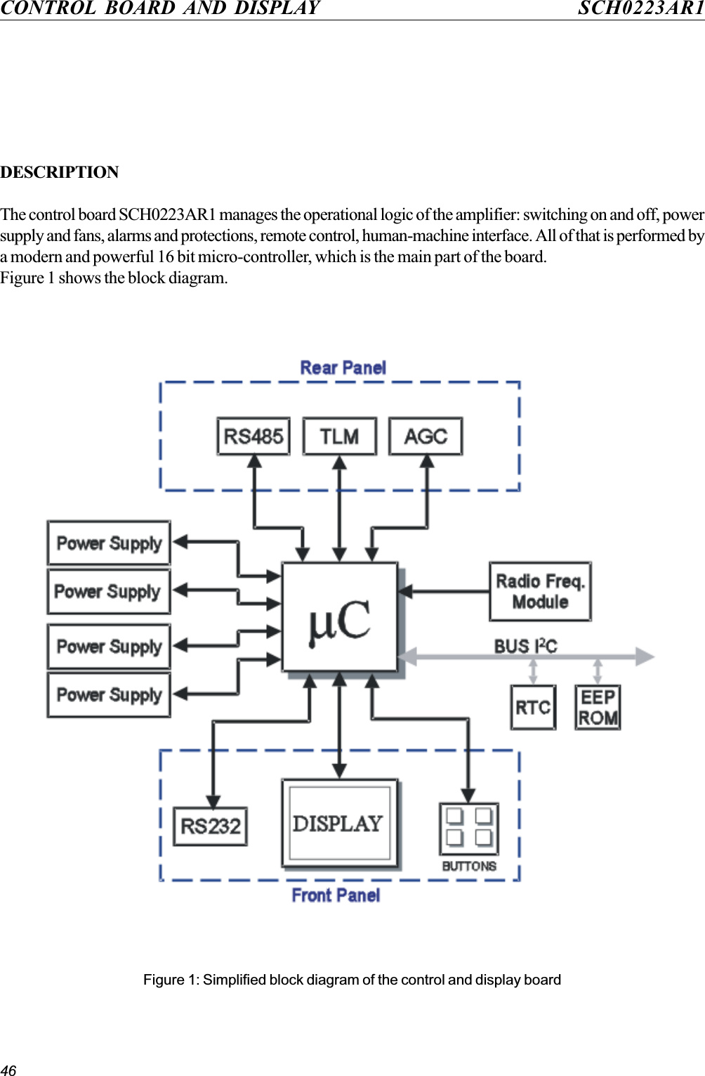
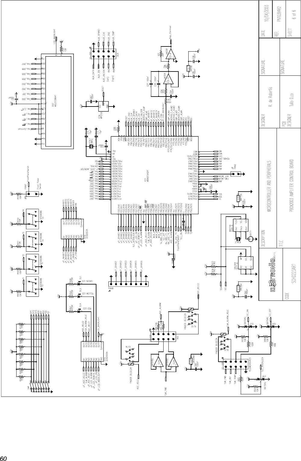
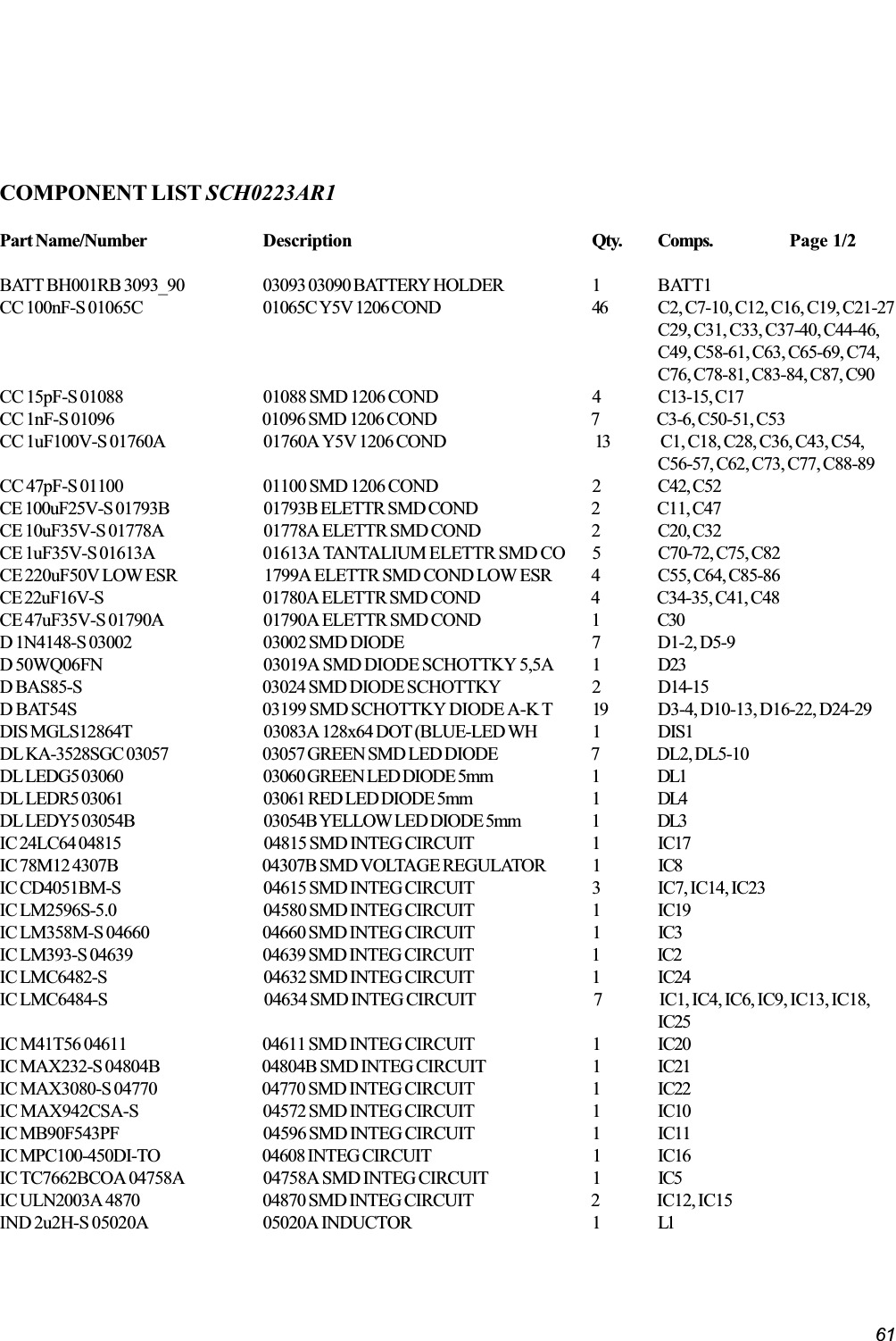
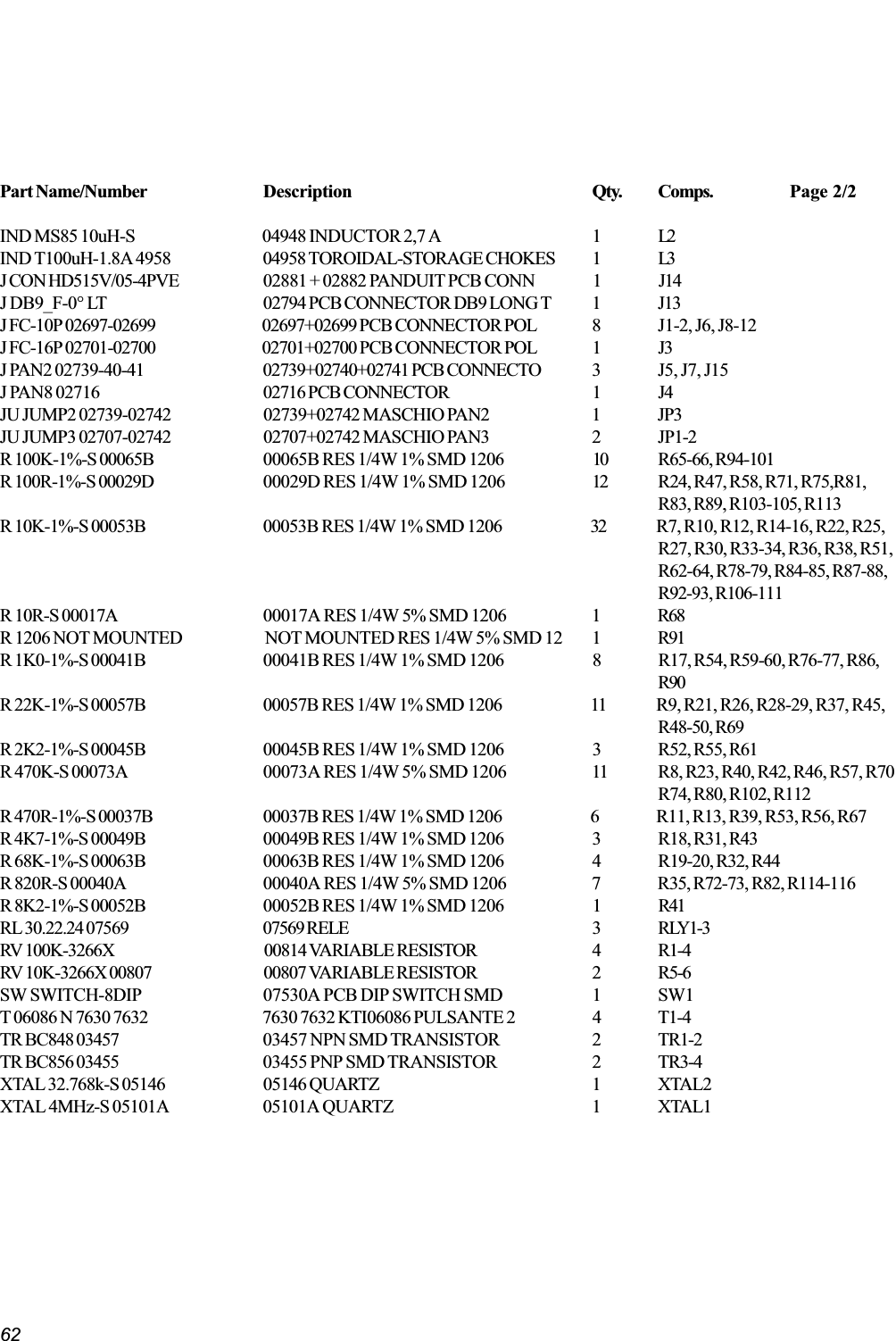
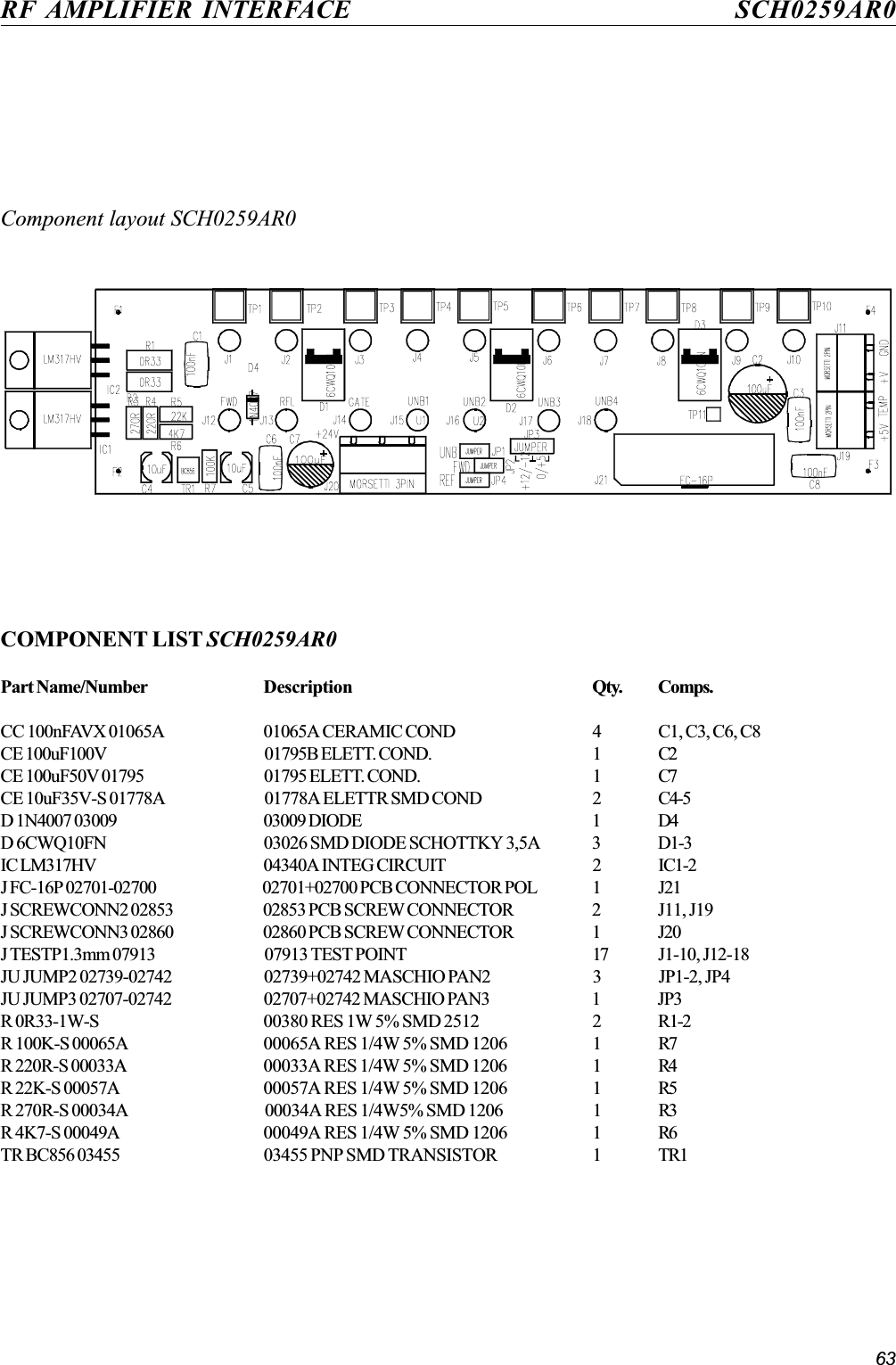
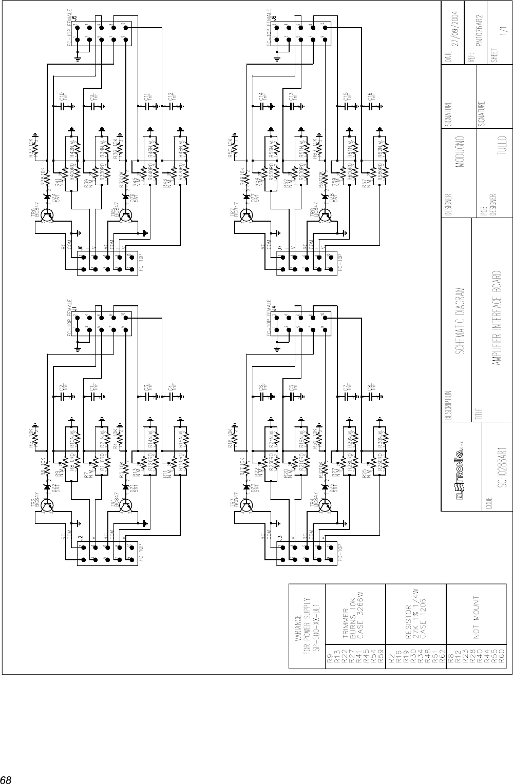
Amplifier User Manual Part 2