EA Technology UTP2A UltraTEV Plus2 User Manual WL18xx Module Hardware Integration Guide
EA Technology Limited UltraTEV Plus2 WL18xx Module Hardware Integration Guide
UserManual.wiki
>
EA Technology
>
UTP2A User Manual
>
User Manual
Contents
1.
User manual
2.
Users manual
3.
User Manual
User Manual
Navigation menu
Upload a User Manual
Namespaces
Wiki Guide
HTML
PDF
Info
Views
User Manual
Discussion / Help
Navigation
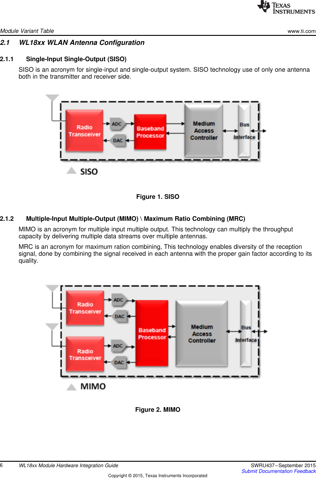
![User's GuideSWRU437–September 2015WL18xx Module Hardware Integration Guide1 IntroductionThis document provides the necessary BT/BLE and WLAN hardware operation information to aid insystem design. This is a review of the integration process of TI's WL18XX Module into final product PCB.When designing your own system around the TI module, it is recommended to step through the guidelinesoutlined below.•WL18xxMOD product page [1]NOTE: You can check your TI module WL18XXMOD design to PCB integration with theWL18XXMOD series of easy-to-follow excel Checklist.WiLink is a trademark of Texas Instruments.Bluetooth is a registered trademark of Bluetooth SIG, Inc. and is licensed to Texas Instruments.Windows is a registered trademark of Microsoft Corporation in the United States and other countries.All other trademarks are the property of their respective owners.4WL18xx Module Hardware Integration Guide SWRU437–September 2015Submit Documentation FeedbackCopyright © 2015, Texas Instruments Incorporated](https://usermanual.wiki/EA-Technology/UTP2A.User-Manual/User-Guide-3906347-Page-4.png)
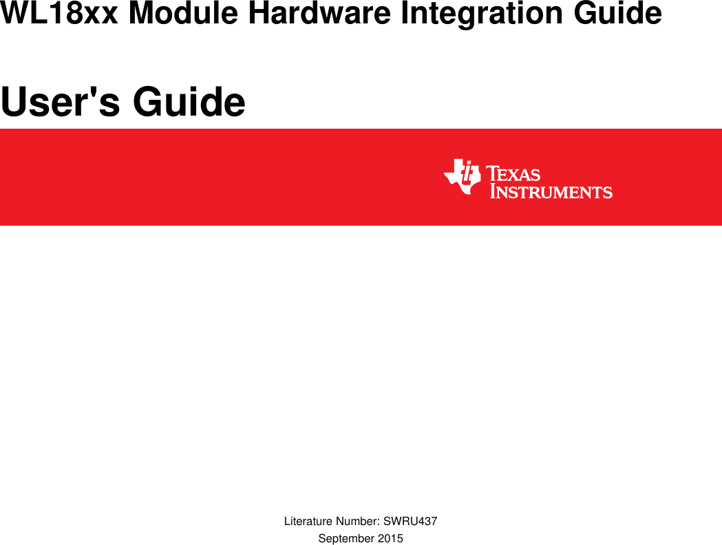
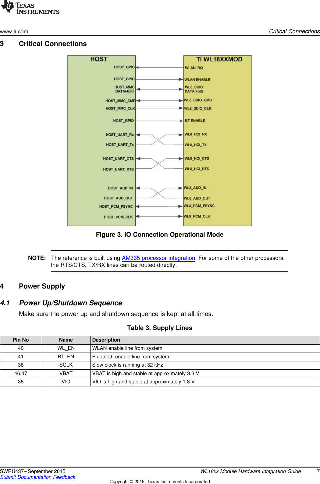
![www.ti.comModule Variant Table2 Module Variant TableTable 1. WL18XXMODGB (2.4 GHz only module variants)WLANReduced integration interfaces Compared to the 2.4-GHz WLAN 2.4-GHz WLANDevice Main 1835 Module SISO MIMO 2.4-GHz MRC BluetoothWL1835MOD • Full version (all of the integration checklist must be ✓ ✓ ✓ ✓applied)WL1831MOD • Only the main RF antenna, ANT1 is used and the ✓ ✓second one should be left N.C.WL1805MOD • For BT IP removal. BT EN line must be connected to ✓ ✓ ✓VSS. BT HCI, PCM and logger lines should be left N.C.WL1801MOD • Only the main RF antenna, ANT1, is used and the ✓second one should be left N.C.• For BT IP removal. BT EN line must be connected toVSS. BT HCI, PCM and logger lines should be left N.C.Table 2. WL18X7MODGI (2.4 GHz and 5 GHz modules)RedundantCapabilitiesCompared to theMain 1837 WLAN WLAN WLAN WLANDevice Module 2.4-GHz SISO (1) 2.4-GHz MIMO (2) 2.4-GHz MRC (3) Bluetooth 5-GHz SISOWL1837MOD • Full version (all ✓✓✓✓✓of the integrationchecklist must beapplied)WL1807MOD • For BT IP ✓ ✓ ✓ ✓removal: BT ENline must beconnected toVSS. BT HCI,PCM and loggerlines should beleft N.C.(1) Single input, single output (SISO)(2) Multiple input, multiple output (MIMO)(3) Maximum ratio combining (MRC)NOTE: Customers working with WL1837MOD/WL1807MOD modules that require only the singleantenna solution (2.4 Ghz WLAN SISO/ BT/ 5 GHz single antenna), while reusing theoriginal certification, can do so by making sure that no RF comes out of the second antennaport (2.4 MIMO only / 5 Ghz diversity). To do this, use the following requirements:• Leave the second module RF port open ( pin number 18 = N.C.)• In the WL1837MOD INI [4], make sure that only 1 antenna is selected for 2.4 GHz bysetting parameter NumberOfAssembledAnt2_4 = 1;5SWRU437–September 2015 WL18xx Module Hardware Integration GuideSubmit Documentation Feedback Copyright © 2015, Texas Instruments Incorporated](https://usermanual.wiki/EA-Technology/UTP2A.User-Manual/User-Guide-3906347-Page-5.png)
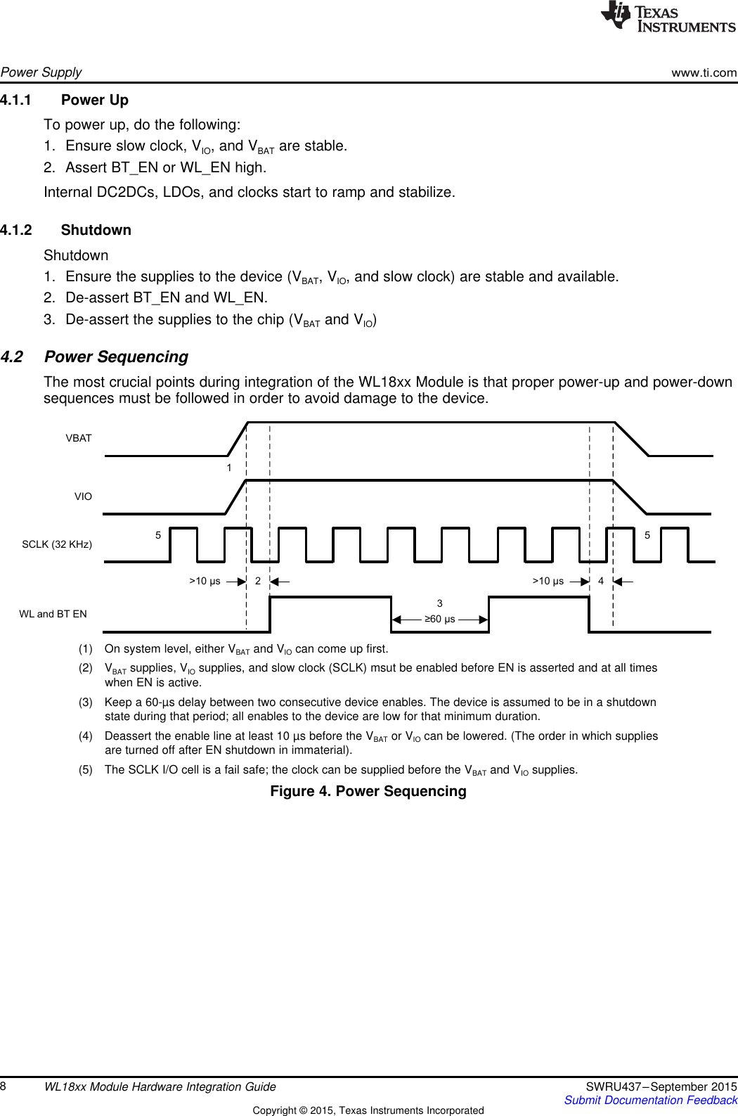
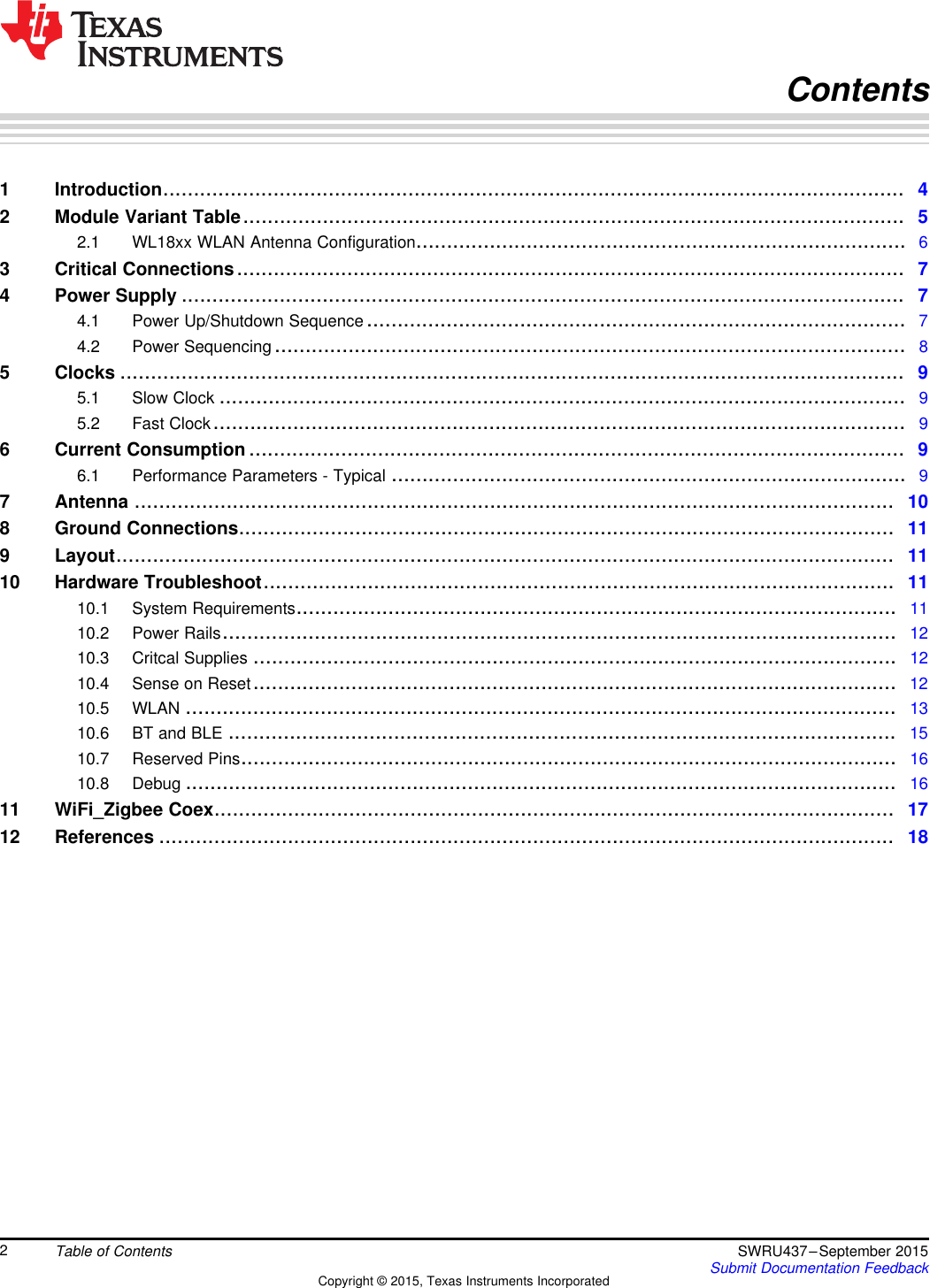
![www.ti.comGround ConnectionsFigure 6. RNR Configuration• Antenna should be placed away from the rest of the circuit– Avoid digital and analog routing in the area, metal enclosure.• MIMO antenna spacing– Distance between the two antennas is advised to be greater than half of the wavelength (62.5 mmat 2.4 GHz)8 Ground ConnectionsAll the ground pins of the module must be connected to ground on the main PCB.9 LayoutFor more information, see the WL1837 User's Guide [5].10 Hardware TroubleshootThis section is intended to cover the basic hardware troubleshoot that you may come across bringing upthe WL18xxMOD on the final board; the device has several interfaces and sequences that must be kept inorder to operate the device in properly.10.1 System RequirementsFor basic integration, the process requires the following components:• Wireless Tool Package located at TI.COM• Minimum requirements: PC running Pentium II• Operating systems: Windows®2000, Windows XP, Windows 7• Serial communication port (RS-232) or USB port with UART-to-USB adapter (to enable the RS232interface on the WiLink 8.0 IC)• Access to WL_UART_DBG pin• Access to BT_UART_DBG• Access to RS232 Tx , RS232 Rx Pins– HCI UART Pins• Oscilloscope• Multimeter11SWRU437–September 2015 WL18xx Module Hardware Integration GuideSubmit Documentation Feedback Copyright © 2015, Texas Instruments Incorporated](https://usermanual.wiki/EA-Technology/UTP2A.User-Manual/User-Guide-3906347-Page-11.png)
![Hardware Troubleshootwww.ti.comDebug and calibration tools for WLAN and Bluetooth®require four UART ports. The most efficient way todrive these ports to the PC is to use a UART-to-USB converter (not included in the wireless toolspackage). TI recommends using the WL18XXCOM82SDMMC SDMMC-to-COM8 adapter with the TIWL1837MODCOM8I module or the WL1835MODCOM8B module on the COM8 board.NOTE: Multiple UART-to-COM8 adapters are available on the market, such as the FTDI Chipdevelopment modules.10.2 Power RailsThere are two power rails that must feed into the WL18xx system:• VBAT - Main power supply source (typically 3.3 V - 3.6 V)– VBAT should be connected to pin 46 and 47 of the module• VIO - Voltage reference from host (1.8 V)– VIO should be connected to pin 38 of the module– Can be used for Level shifter supply and slow clock OSC supply10.3 Critcal SuppliesMake sure all of the critical supplies are in the range of the following expected values:Table 6. Critical SuppliesPin No Name Description Frequency [Hz] Amplitude [V] Current [mA]– DC_IN Depends on the system36 Slow Clock External 32 kHz slow clock 32K 1.8 –46,47 VBAT DC supply range for all modes – 3.3-3.6 100038 VIO I/O ring power supply voltage – 1.8 2001. VBAT and VIO amplitude and current are maximum values.10.4 Sense on ResetWilink8 has several wake-up options that are entered through sense on reset by three IO's of the device:IRQ_WL, UART_DBG_BT, AUD_OUT_BT.Once BT or WLAN enable bit is set to high, the device checks the state of the lines and wakes up in thatspecific mode.There are only two modes or configurations that are supported by the device, all of the rest are prohibitedand the user must verify that there is no option on the system level to enter the prohibited modes.The supported modes are:• Operational mode:– IRQ_WL = 0, UART_DBG_BT = 1, AUD_OUT_BT = 0Operational mode is set by default using internal pull of WL18xx (90K typical).• Debug mode:WLAN RS232 debug interface and Jtag interface are muxed out to the WL18XX IO's by default,nevertheless, this mode is only for debug a 10K resistor pull up place holder on the IRQ line shouldbe placed. It can be applied only in case the debug mode is required:– IRQ_WL = 1, UART_DBG_BT = 1, AUD_OUT_BT = 012 WL18xx Module Hardware Integration Guide SWRU437–September 2015Submit Documentation FeedbackCopyright © 2015, Texas Instruments Incorporated](https://usermanual.wiki/EA-Technology/UTP2A.User-Manual/User-Guide-3906347-Page-12.png)
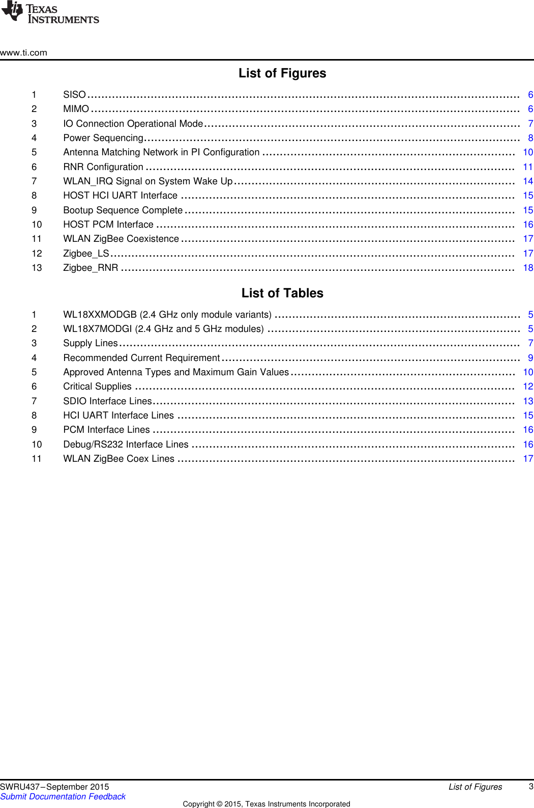
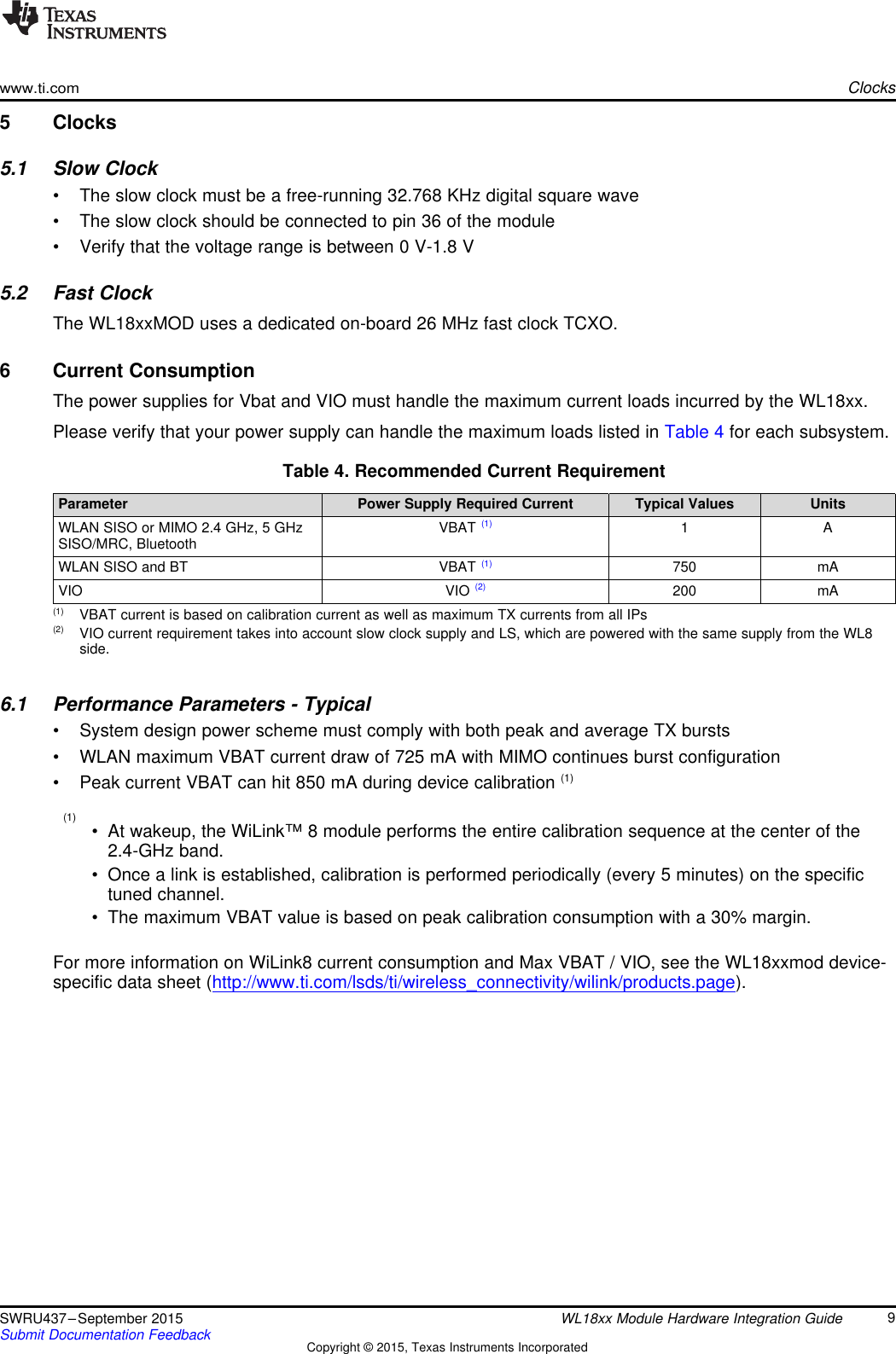
![Hardware Troubleshootwww.ti.comNOTE: It is recommended to connect the SDIO directly to the 1.8 V SDIO interface on the host side.In case Level Shifter is inevitable, see Level Shifting WL18xx I/Os Application Report(SWRA448).10.5.2 WLAN IRQ Operation (SDIO Out-of-Band Interrupt)The WLAN IRQ is an out-of-band interrupt request line that is not defined by the SDIO standardspecification. Therefore, a good understanding on how it works is required in order to work with the WL8xxsolution.The WLAN_IRQ line operates as follows:• The default state of the WLAN_IRQ prior to device enable is internal 100K pulldown (in case of adebug mode there is external 10K pull up)• After the enable line is applied high, the WL_IRQ is changed to drive logic '0'.• During firmware initialization, the WLAN_IRQ is configured by the SDIO module.– The WLAN firmware creates an interrupt-to-host request, indicated by a 0-to-1 transition on theWLAN_IRQ line (the host must be configured as active high or rising-edge detect).– After the host is available, depending on the interrupt priority and other host tasks, it masks thefirmware interrupt. The WLAN_IRQ line returns to 0 (a 1-to-0 transition on the WLAN_IRQ line).– The host reads the internal register status to determine the interrupt sources. The register iscleared after the read.– The host processes all the interrupts read from this register in sequence.– The host unmasks the firmware interrupts.• The host is ready to receive another interrupt from the WLAN device.Figure 7. WLAN_IRQ Signal on System Wake UpFor more details on the Wake on Wlan feature, see [3].14 WL18xx Module Hardware Integration Guide SWRU437–September 2015Submit Documentation FeedbackCopyright © 2015, Texas Instruments Incorporated](https://usermanual.wiki/EA-Technology/UTP2A.User-Manual/User-Guide-3906347-Page-14.png)