DETECTION MONITORING TECHNOLOGIES AIMSFS-05X AIMS FAST SCAN RADAR SYSTEM (AIMSFS-05X) User Manual MSM855 Detailed
DETECTION MONITORING TECHNOLOGIES, LLC (dba DMT, LLC) AIMS FAST SCAN RADAR SYSTEM (AIMSFS-05X) MSM855 Detailed
UserManual.wiki
>
DETECTION MONITORING TECHNOLOGIES
>
AIMSFS-05X User Manual
>
User Manual 1A
Contents
1.
User Manual 1A
2.
User Manual 1B
3.
User Manual 2
4.
Installation Guide 1
5.
Installation Guide 2
6.
Installation Guide 3
User Manual 1A
Navigation menu
Upload a User Manual
Namespaces
Wiki Guide
HTML
PDF
Info
Views
User Manual
Discussion / Help
Navigation
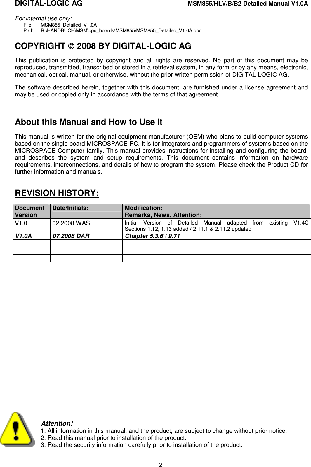

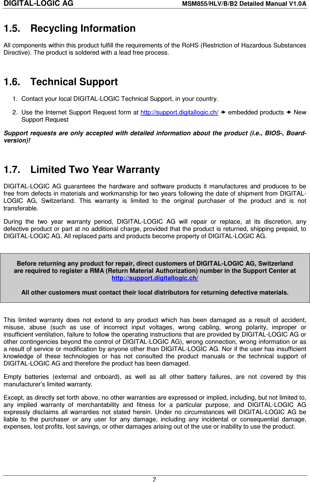
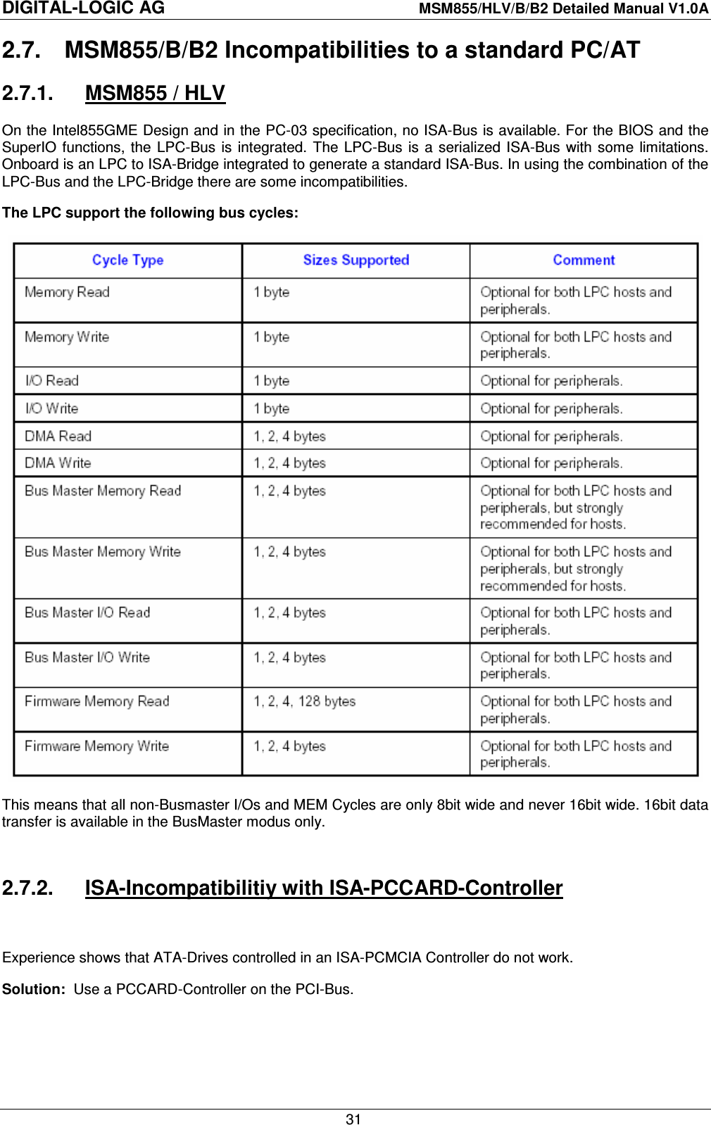
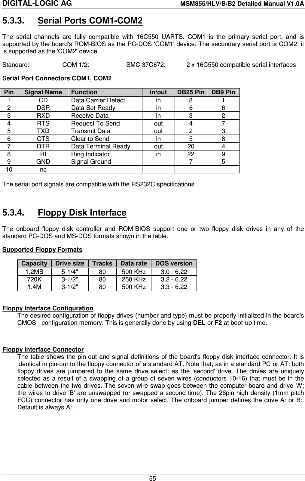
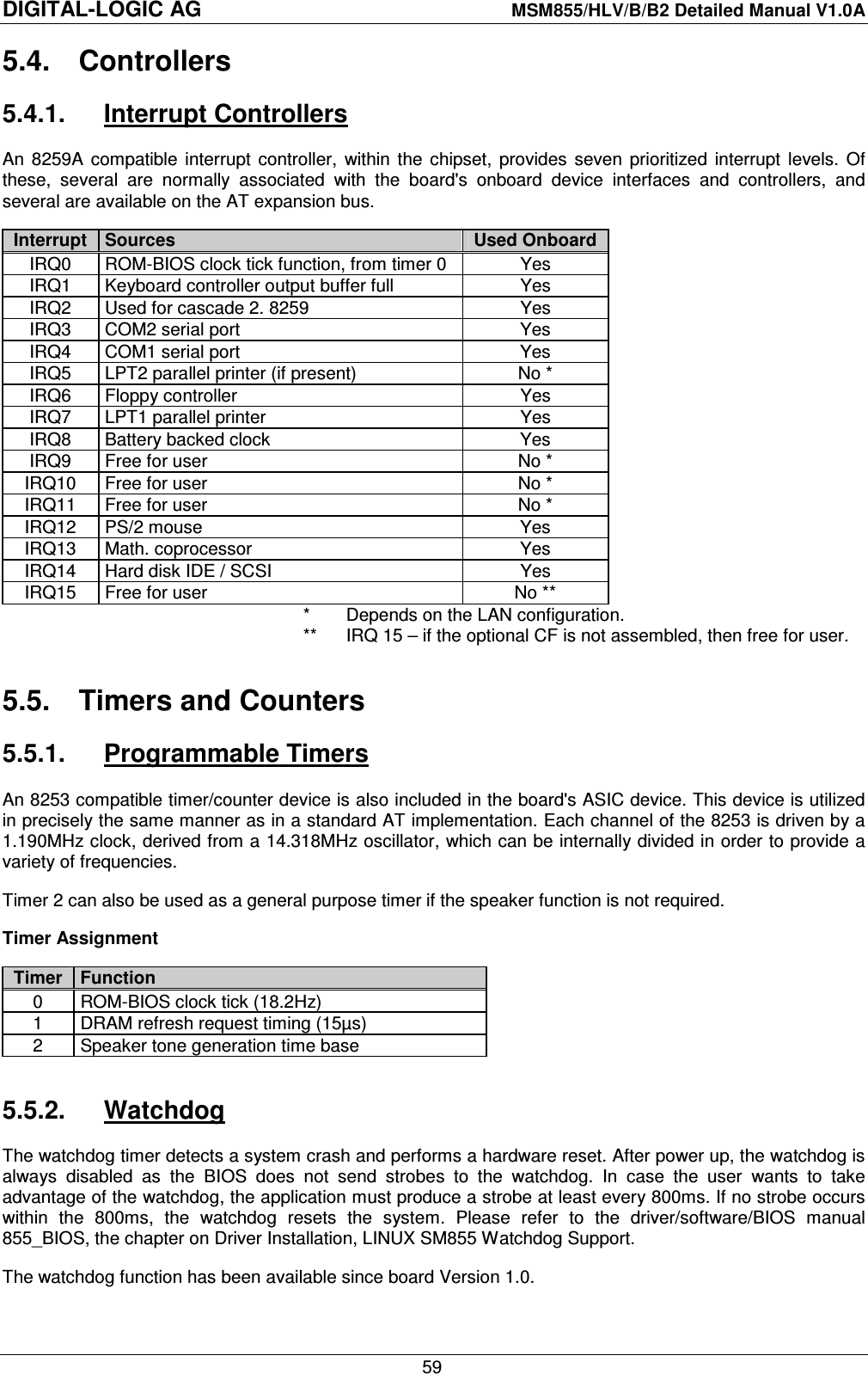
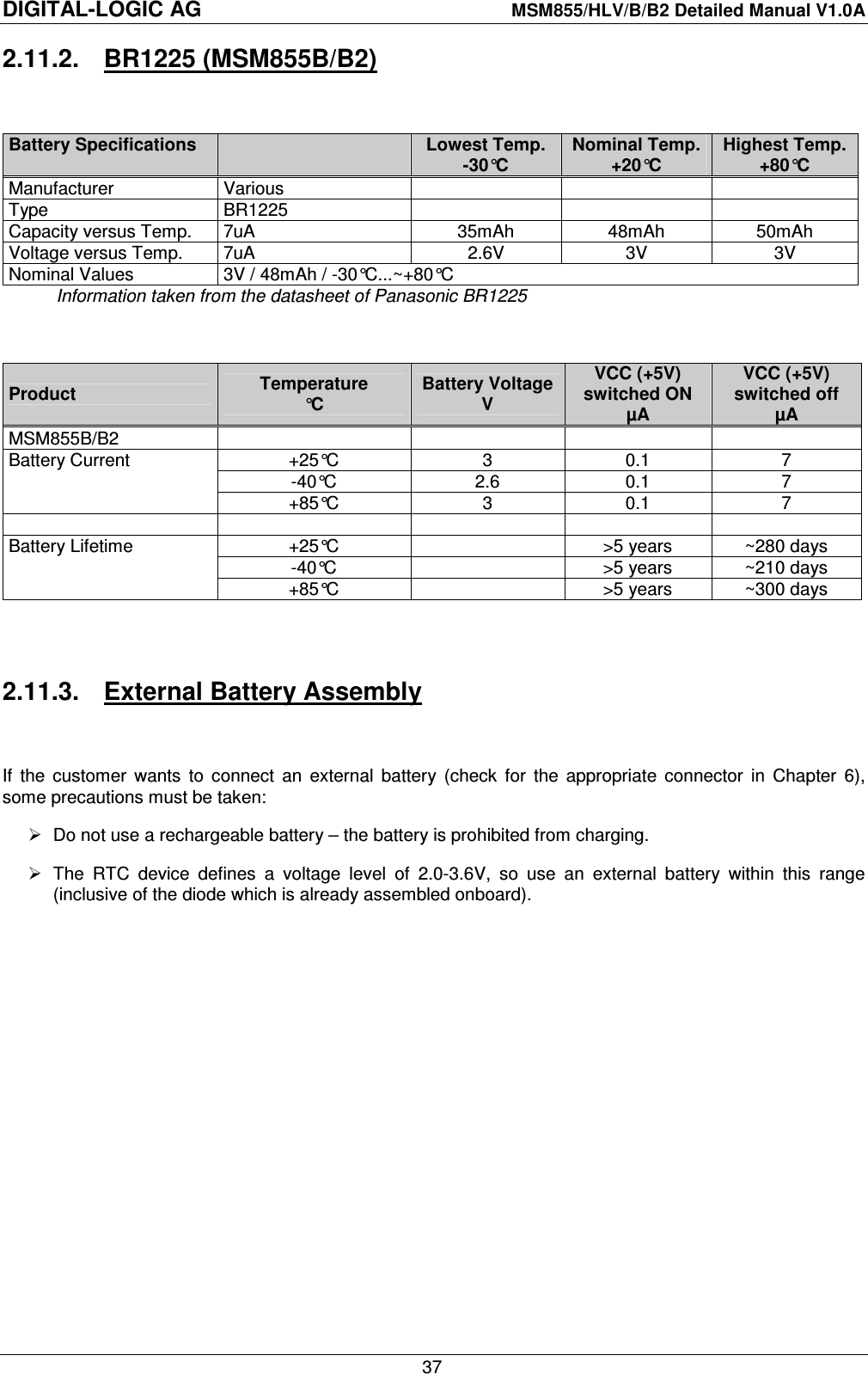
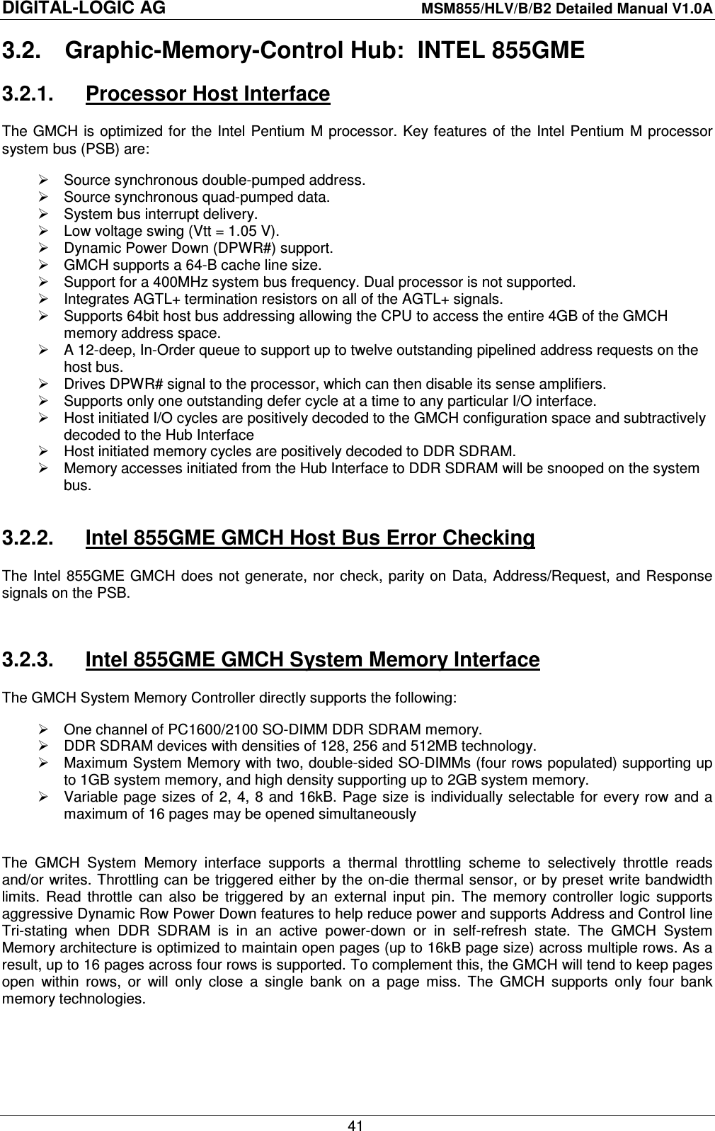
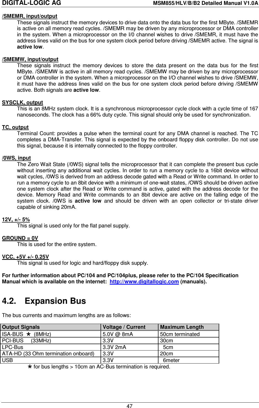
![DIGITAL-LOGIC AG MSM855/HLV/B/B2 Detailed Manual V1.0A 33 2.9. Thermoscan Equipment: Product Part Number Serial Number Version MSM855 803010 46201010507 1.1 SM855-11P 1.1GHz 805161 45216110026 0.8 SM855-P378 1.4GHz 805164 45316410032 0.8 SODIMM DDR 1GB 870672 - - Software Windows XP SP2 running desk top MSM855-11P Top view t [min] fCPU [MHz] I [A] TSensor[°C] TCPU[°C] THS[°C] P [W] 60 1100 3.65 65 69 63 18.6 MSM855-11P Bottom view: t [min] fCPU [MHz] I [A] TSensor[°C] TCPU[°C] TKK[°C] P [W] 60 1100 3.68 67 72 65 18.8](https://usermanual.wiki/DETECTION-MONITORING-TECHNOLOGIES/AIMSFS-05X.User-Manual-1A/User-Guide-1532461-Page-33.png)
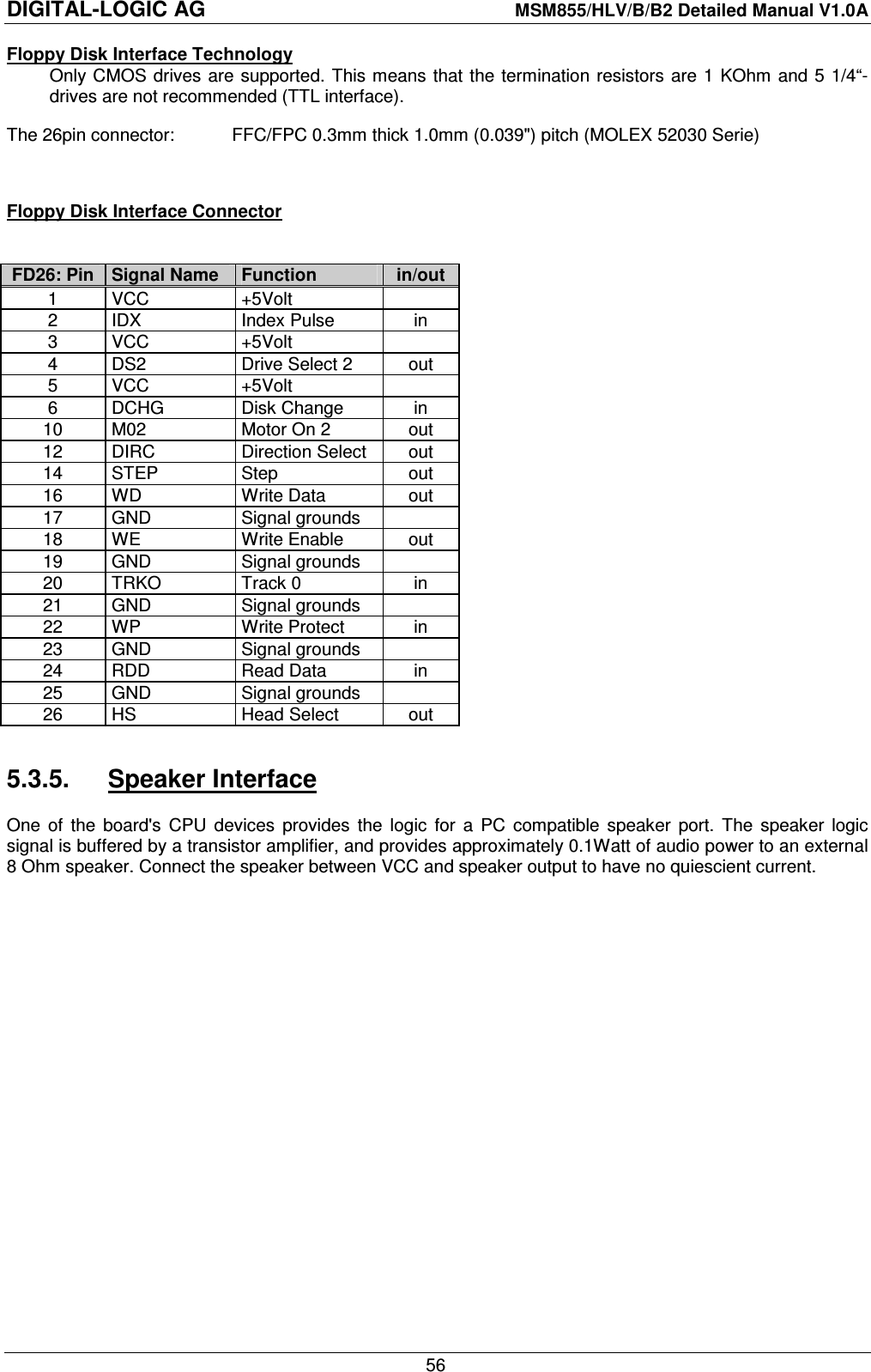
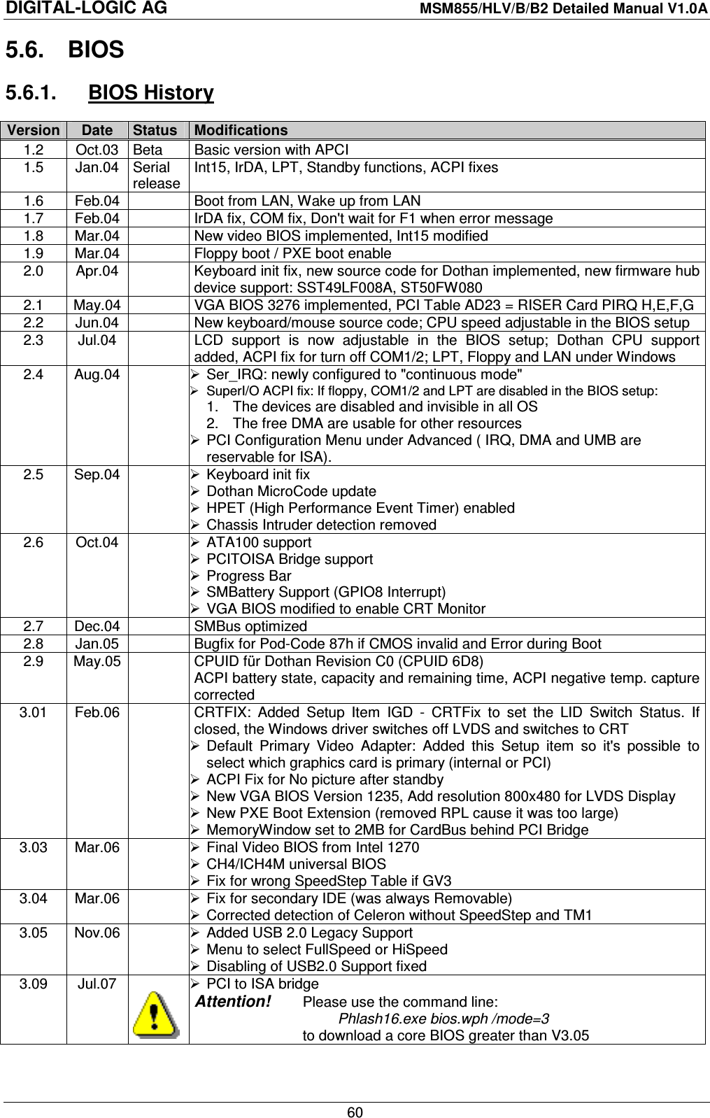
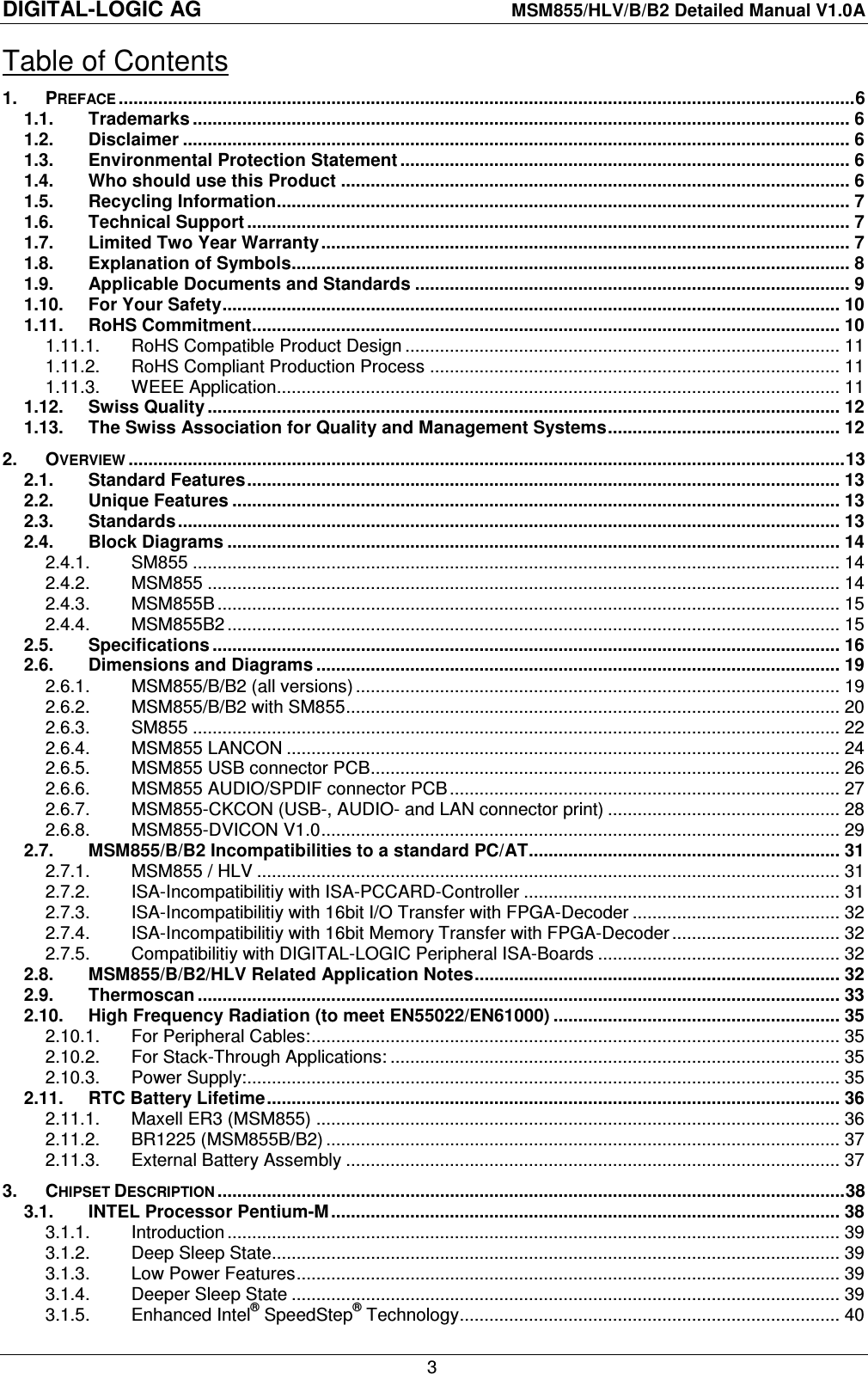
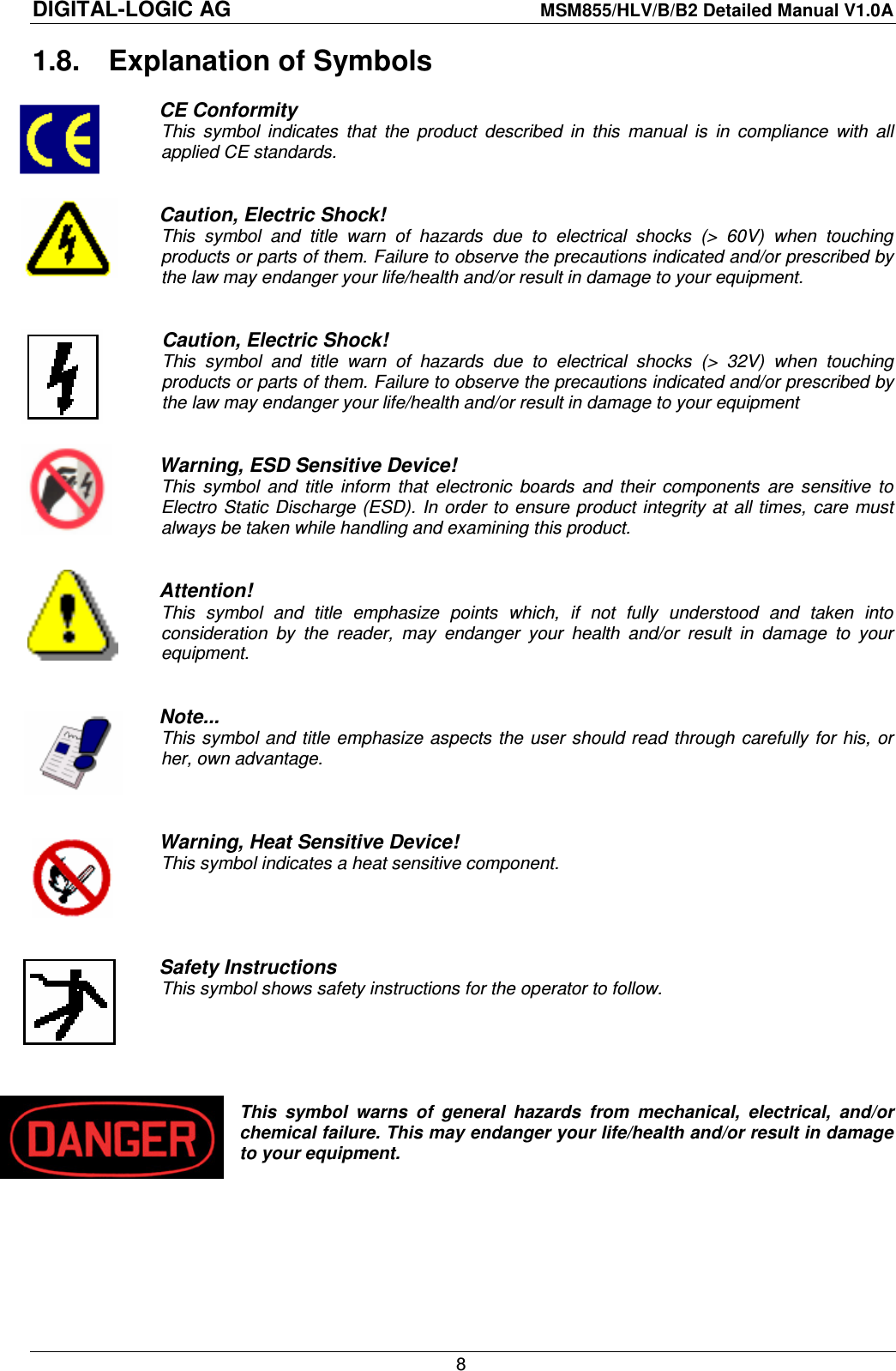
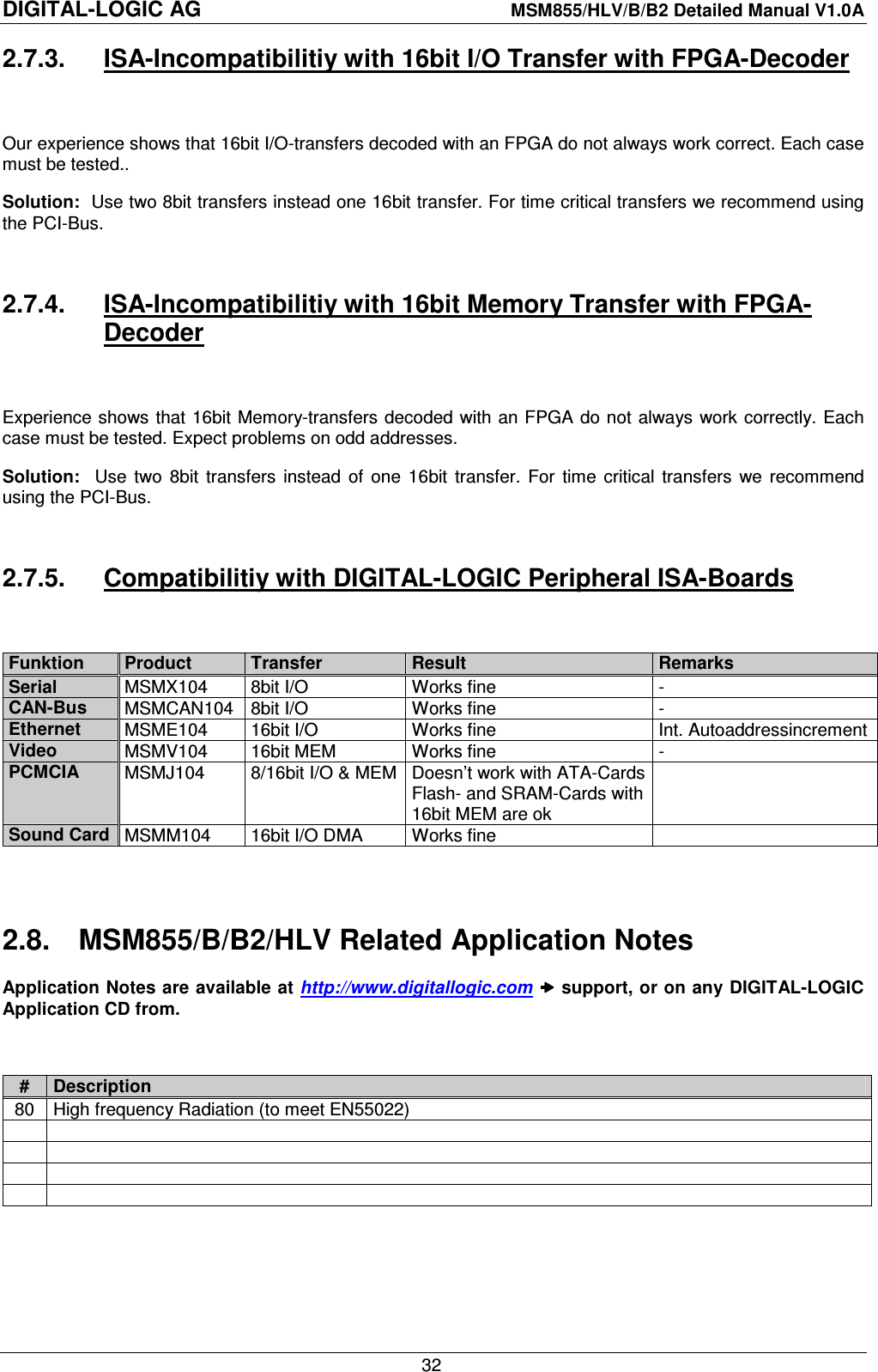
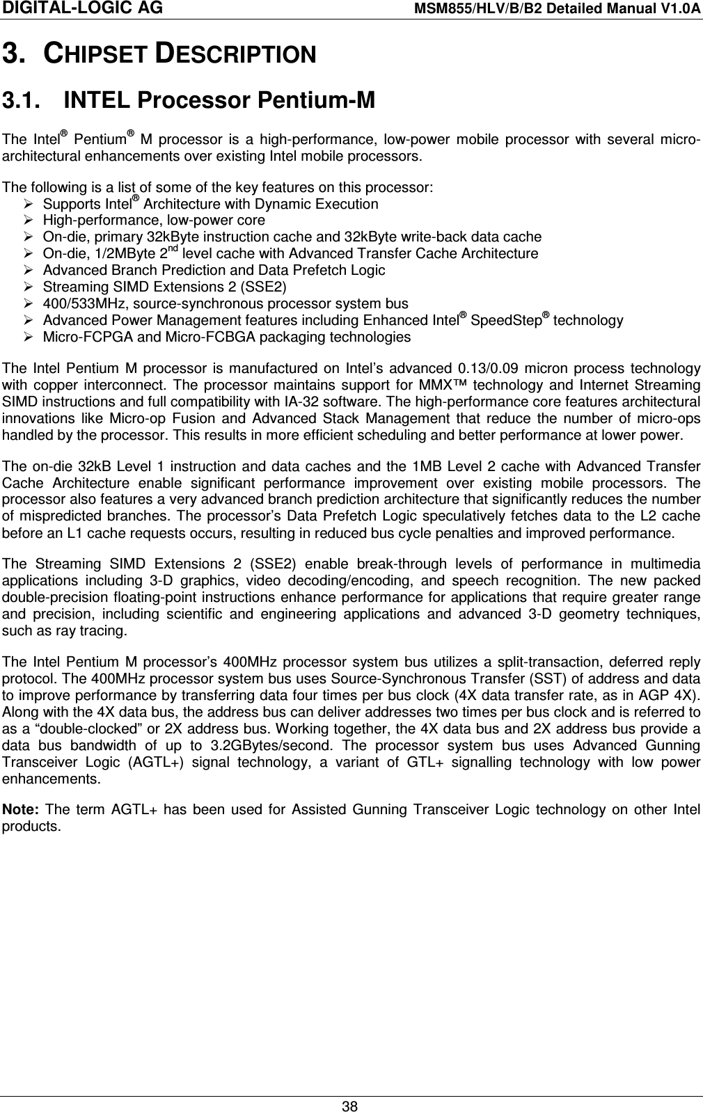
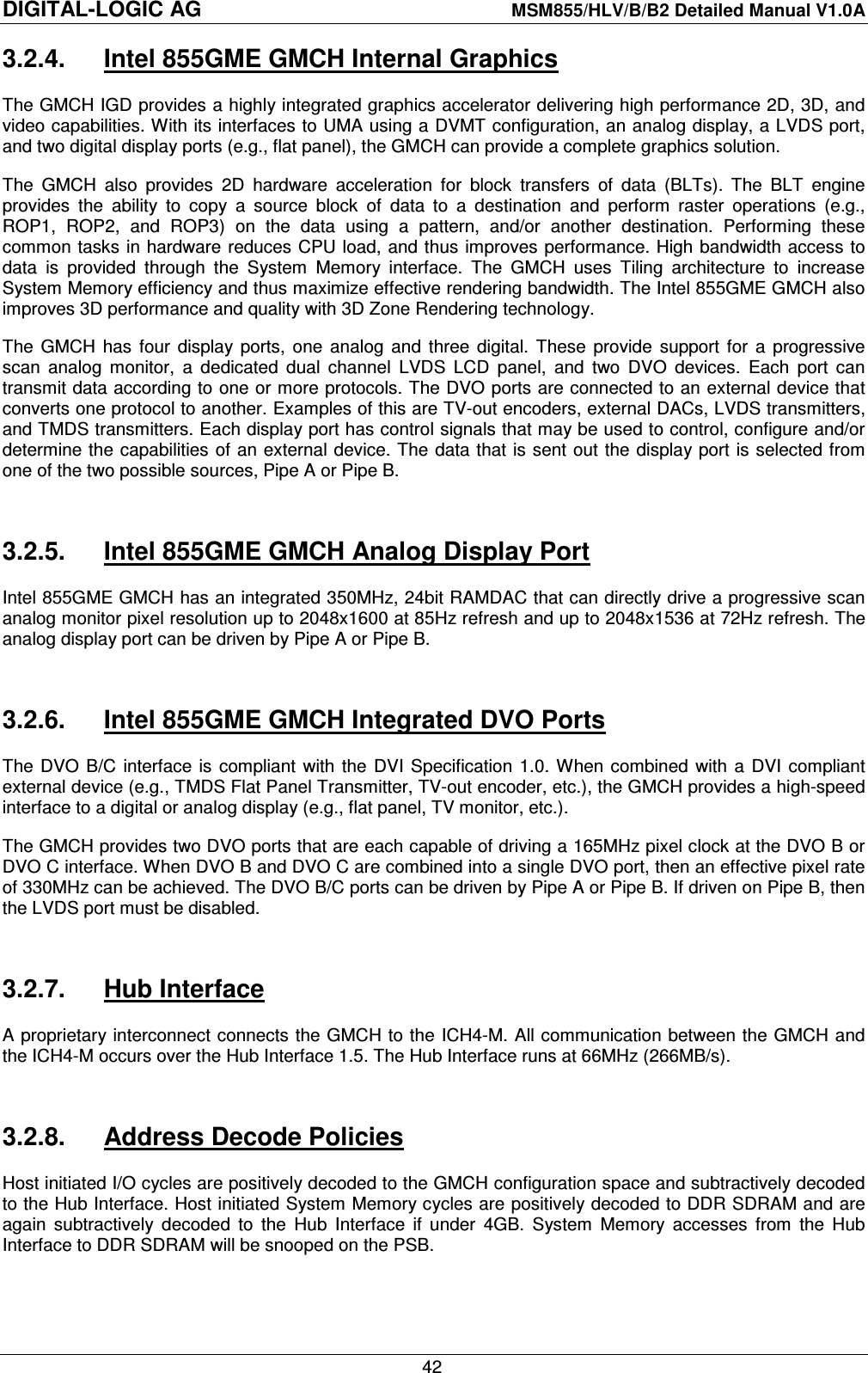
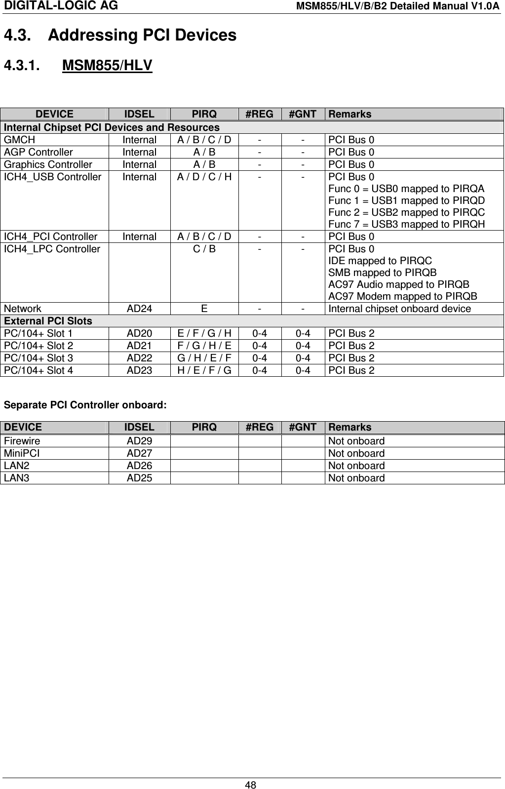
![DIGITAL-LOGIC AG MSM855/HLV/B/B2 Detailed Manual V1.0A 34 MSM855-738 Top view: t [min] fCPU [MHz] I [A] TSensor[°C] TCPU[°C] THS[°C] P [W] 60 1400 3.58 42 47 32 18.3 MSM855-738 Bottom view: t [min] fCPU [MHz] I [A] TSensor[°C] TCPU[°C] THS[°C] P [W] 60 1400 3.65 53 59 44 18.6](https://usermanual.wiki/DETECTION-MONITORING-TECHNOLOGIES/AIMSFS-05X.User-Manual-1A/User-Guide-1532461-Page-34.png)
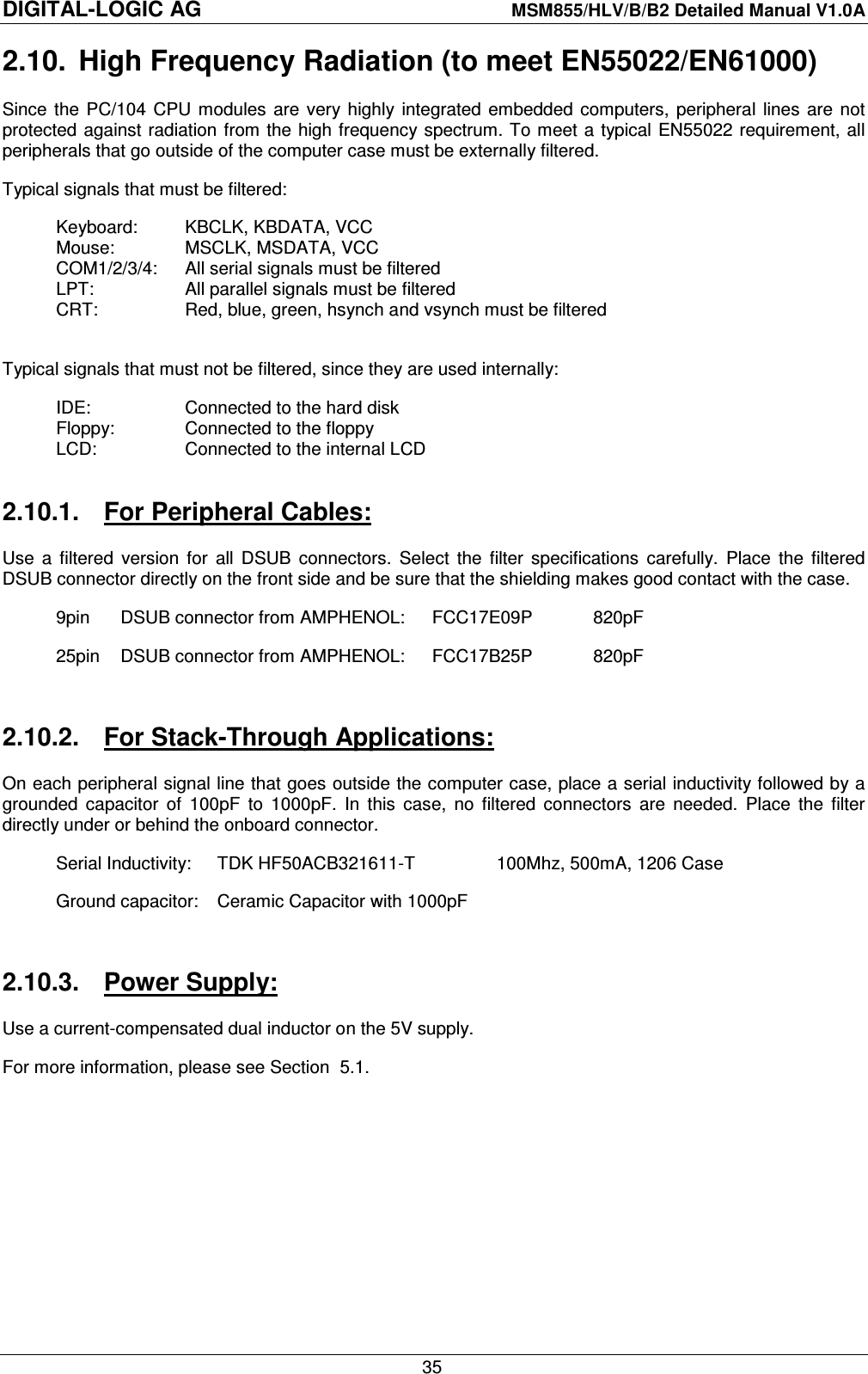
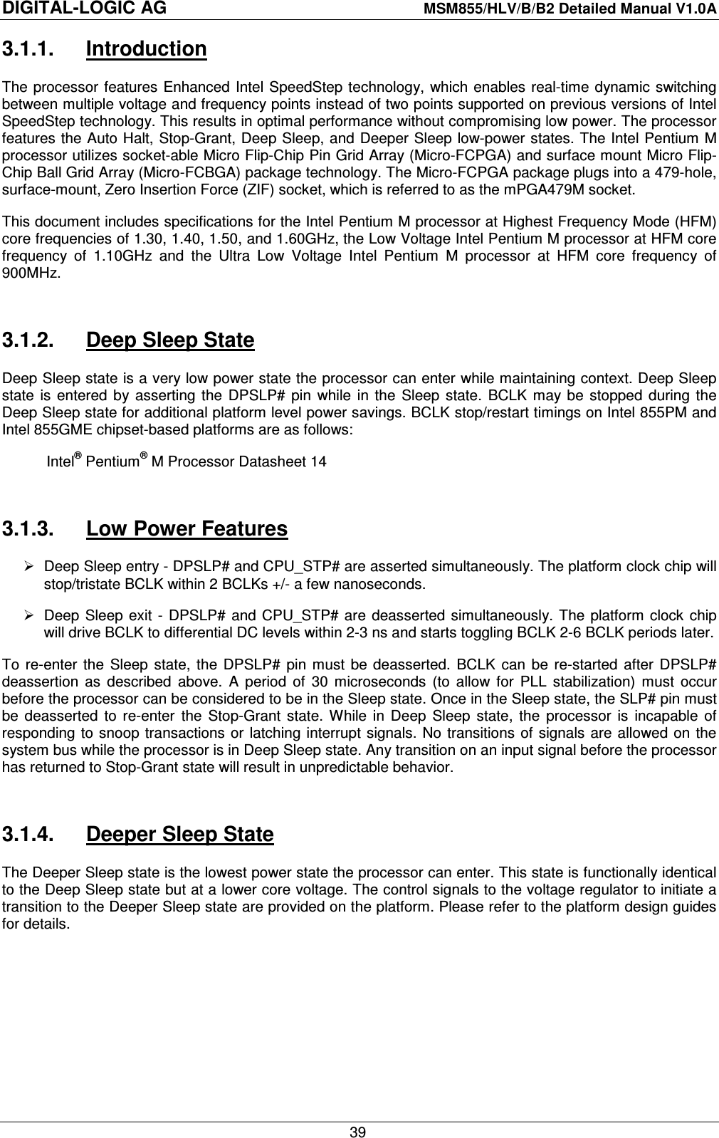
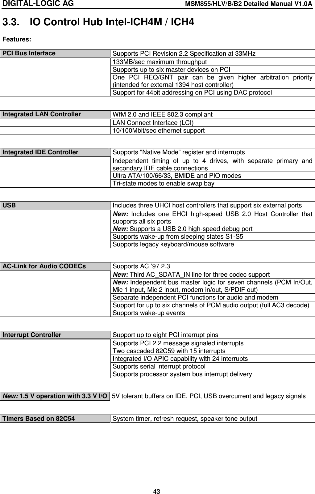
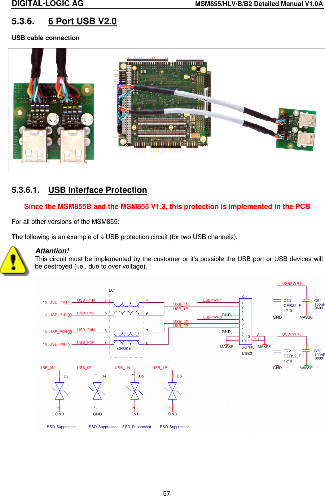
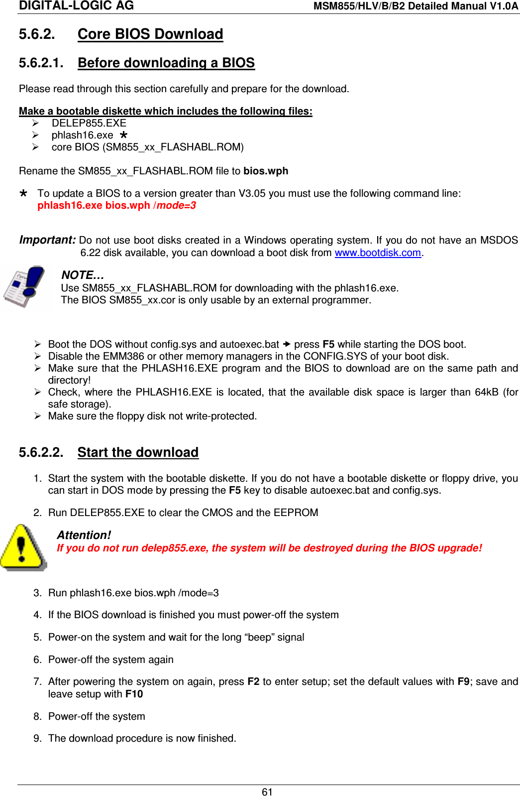
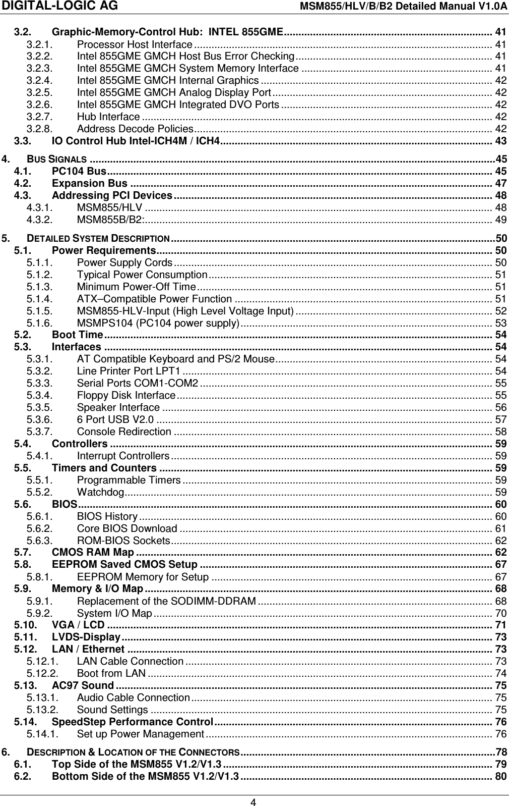
![DIGITAL-LOGIC AG MSM855/HLV/B/B2 Detailed Manual V1.0A 45 4. BUS SIGNALS 4.1. PC104 Bus Note... Not all of the signals are available on this board (please see Chapter 6 for a description of the connectors). AEN, output Address Enable: used to degate the microprocessor and other devices from the I/O channel to allow DMA transfers to take place. low = CPU Cycle, high = DMA Cycle BALE, output Address Latch Enable: provided by the bus controller and used on the system board to latch valid addresses and memory decodes from the microprocessor. This signal is used so that devices on the bus can latch LA17-23. The SA0-19 address lines latch internally according to this signal. BALE is forced high during DMA cycles. /DACK[0, 5-7], output DMA Acknowledge: 0 to 3 and 5 to 7 are used to acknowledge DMA requests (DRQO through DRQ7). They are active low. This signal indicates that the DMA operation can begin. DRQ[0, 5-7], input DMA Requests: 0 through 3 and 5 through 7 are asynchronous channel requests used by peripheral devices and the I/O channel microprocessors to gain DMA service (or control of the system). A request is generated by bringing a DRQ line to an active level. A DRQ line must be held high until the corresponding DMA Request Acknowledge (DACK/) line goes active. DRQO through DRQ3 will perform 8bit DMA transfers; DRQ5-7 are used for 16 accesses. /IOCHCK, input IOCHCK/: provides the system board with parity (error) information about memory or devices on the I/O channel. low = parity error, high = normal operation IOCHRDY, input I/O Channel Ready: pulled low (not ready) by a memory or I/O device to lengthen I/O or memory cycles. Any slow device using this line should drive it low immediately upon detecting its valid address and a Read or Write command. Machine cycles are extended by an integral number of one clock cycle (67 nanoseconds). This signal should be held in the range of 125-15600nS. low = wait, high = normal operation /IOCS16, input I/O 16 Bit Chip Select: signals the system board that the present data transfer is a 16bit, 1 wait-state, I/0 cycle. It is derived from an address decode. /IOCS16 is active low and should be driven with an open collector (300 ohm pull-up) or tri-state driver capable of sinking 20mA. The signal is driven based only on SA15-SAO (not /IOR or /IOW) when AEN is not asserted. In the 8bit I/O transfer, the default transfers a 4 wait-state cycle. /IOR, input/output I/O Read instructs an I/O device to drive its data onto the data bus. It may be driven by the system microprocessor or DMA controller, or by a microprocessor or DMA controller resident on the I/O channel. This signal is active low. /IOW, input/output I/O Write: instructs an I/O device to read the data on the data bus. It may be driven by any microprocessor or DMA controller in the system. This signal is active low.](https://usermanual.wiki/DETECTION-MONITORING-TECHNOLOGIES/AIMSFS-05X.User-Manual-1A/User-Guide-1532461-Page-45.png)
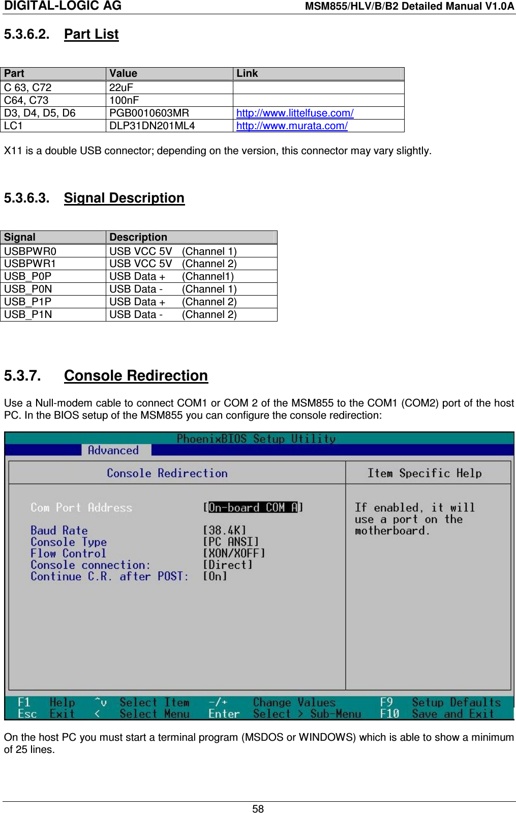
![DIGITAL-LOGIC AG MSM855/HLV/B/B2 Detailed Manual V1.0A 46 IRQ [10, 12, 14, 15], input These signals are used to tell the microprocessor that an I/O device needs attention. An interrupt request is generated when an IRQ line is raised from low to high. The line must be held high until the microprocessor acknowledges the interrupt request. /Master, input This signal is used with a DRQ line to gain control of the system. A processor or DMA controller on the I/0 channel may issue a DRQ to a DMA channel in cascade mode and receive a /DACK. /MEMCS16, input MEMCS16 Chip Select: signals the system board if the present data transfer is a 1 wait-state, 16bit, memory cycle. It must be derived from the decode of LA17 through LA23. /MEMCS16 should be driven with an open collector (300 ohm pull-up) or tri-state driver capable of sinking 20mA. /MEMR, input/output These signals instruct the memory devices to drive data onto the data bus. /MEMR is active on all memory read cycles. /MEMR may be driven by any microprocessor or DMA controller in the system. When a microprocessor on the I/0 channel wishes to drive /MEMR, it must have the address lines valid on the bus for one system clock period before driving /MEMR active. These signals are active low. /MEMW, input/output These signals instruct the memory devices to store the data present on the data bus. /MEMW is active in all memory read cycles. /MEMW may be driven by any microprocessor or DMA controller in the system. When a microprocessor on the I/O channel wishes to drive /MEMW, it must have the address lines valid on the bus for one system clock period before driving /MEMW active. Both signals are active low. OSC, output Oscillator (OSC): a high-speed clock with a 70 nanosecond period (14.31818 MHz). This signal is not synchronous with the system clock. It has a 50% duty cycle. OSC starts 100µs after reset is inactive. RESETDRV, output Reset Drive: used to reset or initiate system logic at power-up time or during a low line-voltage outage. This signal is active high. When the signal is active all adapters should turn off or tri-state all drivers connected to the I/O channel. This signal is driven by the permanent Master. /REFRESH, input/output These signals are used to indicate a refresh cycle and can be driven by a microprocessor on the I/0 channel. These signals are active low. SA0-SA19, LA17 - LA23 input/output Address bits 0 through 19 are used to address memory and I/0 devices within the system. These 20 address lines, allow access of up to 1MBytes of memory. SAO through SA19 are gated on the system bus when BALE is high and are latched on the falling edge of BALE. LA17 to LA23 are not latched and addresses the full 16MByte range. These signals are generated by the microprocessors or DMA controllers. They may also be driven by other microprocessor or DMA controllers that reside on the I/0 channel. The SA17-SA23 are always LA17-LA23 address timings for use with the MSCS16 signal. This is advanced AT96 design. The timing is selectable with jumpers LAxx or SAxx. /SBHE, input/output Bus High Enable (system): indicates a transfer of data on the upper byte of the data bus, XD8 through XD15. Sixteen-bit devices use /SBHE to condition data-bus buffers tied to XD8 through XD15. SD[0-15], input/output These signals provide bus bits 0 through 15 for the microprocessor, memory, and I/0 devices. D0 is the least significant bit and D15 is the most significant bit. All 8bit devices on the I/O channel should use D0 through D7 for communications to the microprocessor. The 16bit devices will use D0 through D15. To support 8bit devices, the data on D8 through D15 will be gated to D0 through D7 during 8bit transfers to these devices; 16bit microprocessor transfers to 8bit devices will be converted to two 8bit transfers.](https://usermanual.wiki/DETECTION-MONITORING-TECHNOLOGIES/AIMSFS-05X.User-Manual-1A/User-Guide-1532461-Page-46.png)
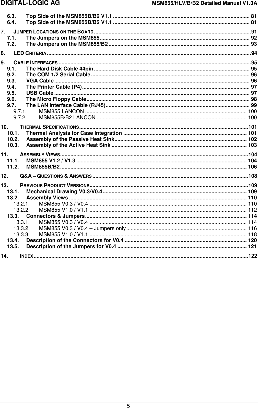
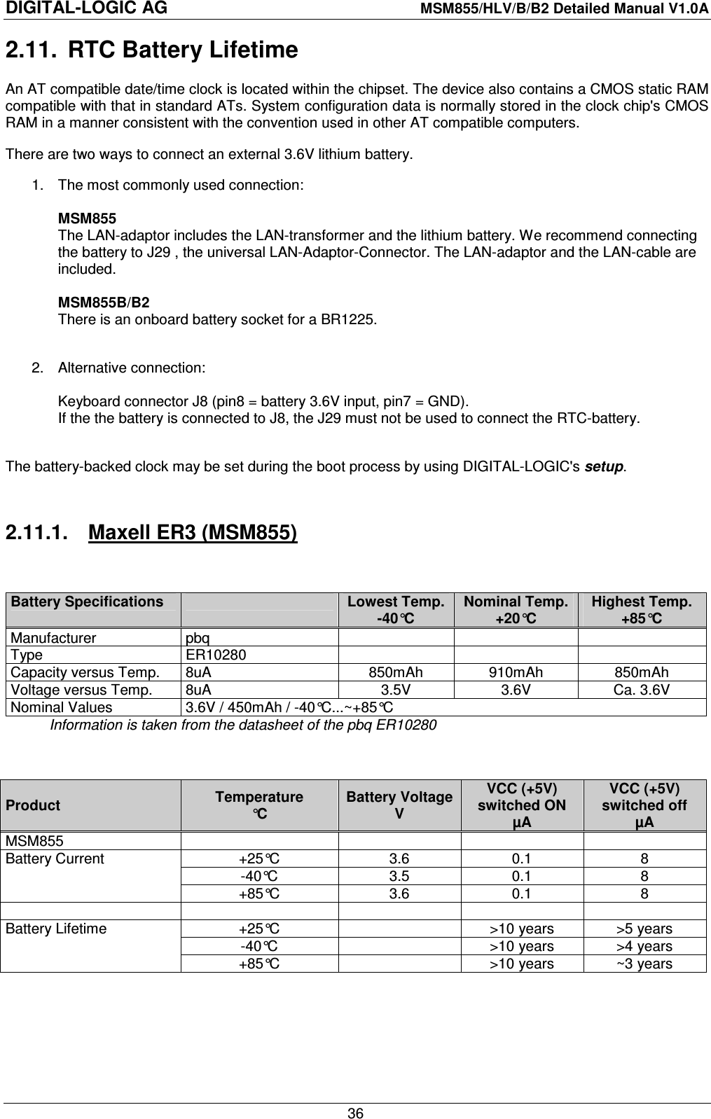
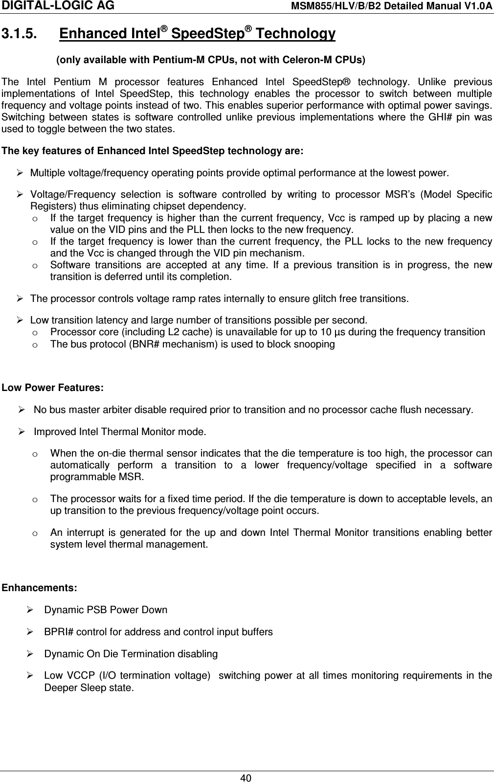
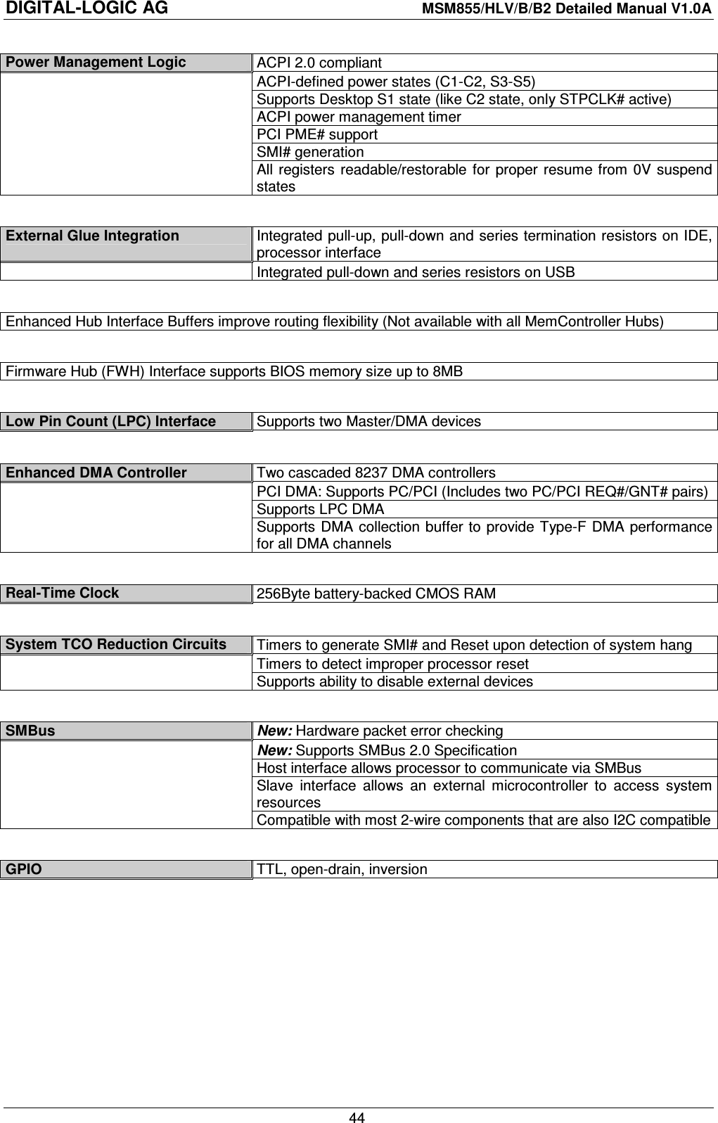
![DIGITAL-LOGIC AG MSM855/HLV/B/B2 Detailed Manual V1.0A 53 5.1.6. MSMPS104 (PC104 power supply) Below is the description of how to connect and configure the MSMPS104 to an MSM855. 5.1.6.1. Necessary Parts MSMPS104, Part Nr. 806032 MSM855, Part Nr. 803010 MSM855-CK Cable Kit, Part Nor. 802032 Spacerkit-PC/104, Part Nr. 802050 or Spacerkit-PC/104-Plus, Part Nr. 802051 (if option PC/104-Plus with connector long [Part Nr. 807006] is installed) 5.1.6.2. Procedure 1. Remove Jumper J2 2. Press the two 2x20 Pin and the 2x32 Pin sockets in the PC/104 connector of the MSMPS104 board. Press the 4x30 Pin socket in the PC/104-Plus connector if that option is installed. Mount the four threaded standoffs with four nuts on the MSMPS104 board. Place the MSM855 board on the PC/104 connector of the MSMPS104 and press it down. Fix the MSM855 board with four screws on the threaded standoffs. Connect both boards together with the cables J2](https://usermanual.wiki/DETECTION-MONITORING-TECHNOLOGIES/AIMSFS-05X.User-Manual-1A/User-Guide-1532461-Page-53.png)
![DIGITAL-LOGIC AG MSM855/HLV/B/B2 Detailed Manual V1.0A 54 5.2. Boot Time System Boot-Times: Definitions/Boot-Medium Quick Boot* Normal Boot MSM855-1600MHz with RTC-backup battery Memory 256MB shared 8MB for video time [s] time [s] From Floppy disk: Boot from Setup-Disk1 MS-DOS v6.22 to "Starting MS-DOS“-Prompt 10 26 Boot from Setup-Disk1 MS-DOS v6.22 to "Welcome Setup Screen“-Prompt 30 45 Boot from "(Sys a:)-Disk“ to "A:/>“-Prompt 18 33 From Hard disk-Toshiba MK2110MAF: Boot from Hard disk to "Starting MS-DOS“-Prompt 10 26 Boot from Hard disk to "Win2000: Windows-Login“-Prompt 80 95 From CompactFlash SunDisk SDCFB-64-101-00 64MB: Boot from CF to "Starting MS-DOS“-Prompt 10 26 Boot from CF to "C:\>“-Prompt 13 29 5.3. Interfaces 5.3.1. AT Compatible Keyboard and PS/2 Mouse Pin Signal 1 Speaker out 2 GND 3 External reset input 4 VCC 5 Keyboard Data 6 Keyboard Clock 7 GND 8 External Battery 9 Mouse Clock (PS/2) 10 Mouse Data (PS/2) 5.3.2. Line Printer Port LPT1 A standard bi-directional LPT port is integrated into the MICROSPACE PC. Further information about these signals is available in numerous publications, including the IBM technical reference manuals for the PC and AT computers and from other reference documents. The current is: IOH = 12mA IOL = 24mA The SMC 37C672 may be programmed via software commands. In the new BIOS version, this selection may be controlled with the BIOS setup screen.](https://usermanual.wiki/DETECTION-MONITORING-TECHNOLOGIES/AIMSFS-05X.User-Manual-1A/User-Guide-1532461-Page-54.png)