Cypress Semiconductor 6045 EZ-BLE PSoC Module User Manual CYBLE 214009 00 EZ BLE PSoC Module
Cypress Semiconductor EZ-BLE PSoC Module CYBLE 214009 00 EZ BLE PSoC Module
UserManual.wiki
>
Cypress Semiconductor
>
6045 User Manual
Users Manual
Navigation menu
Upload a User Manual
Namespaces
Wiki Guide
HTML
PDF
Info
Views
User Manual
Discussion / Help
Navigation
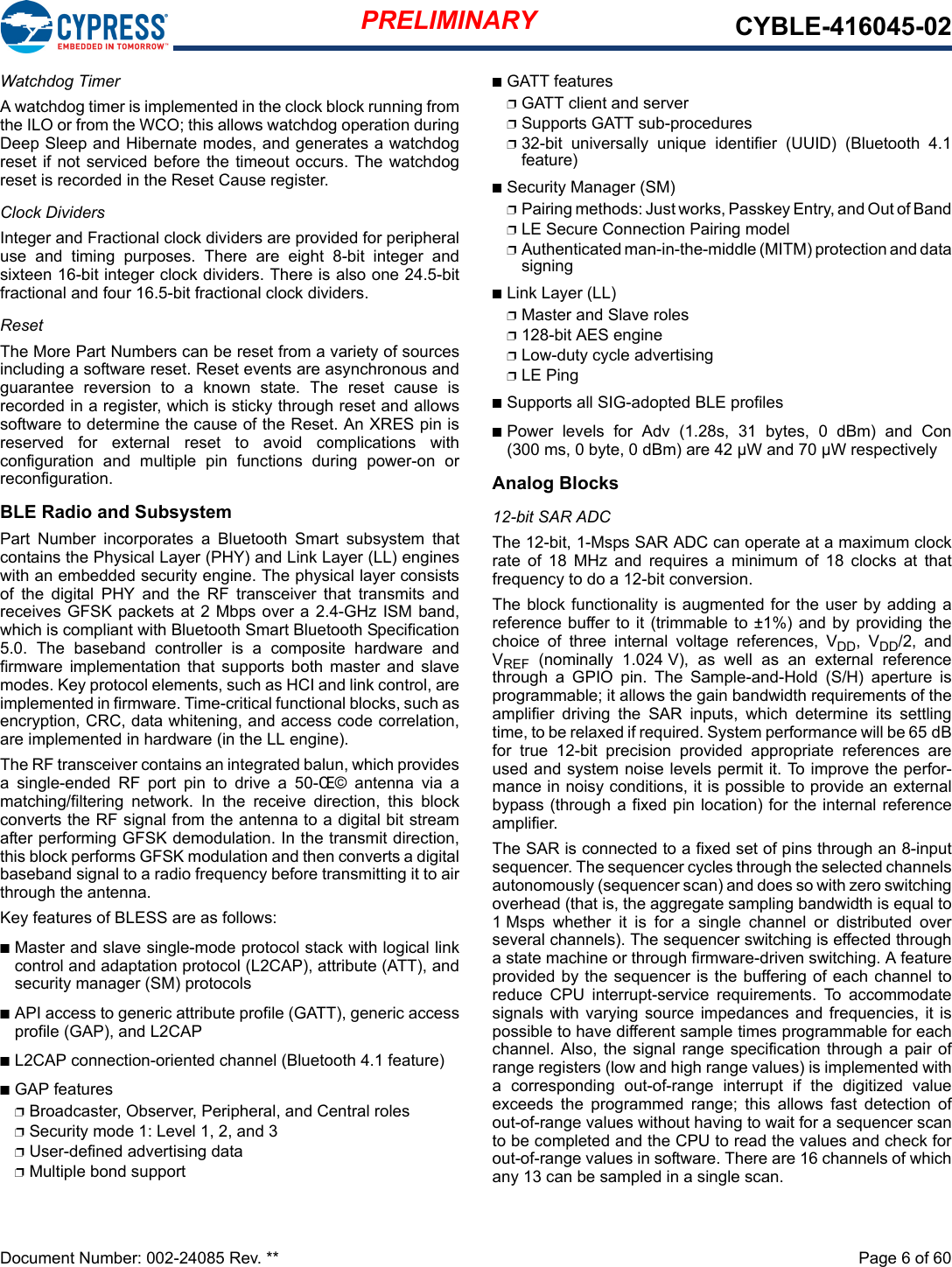
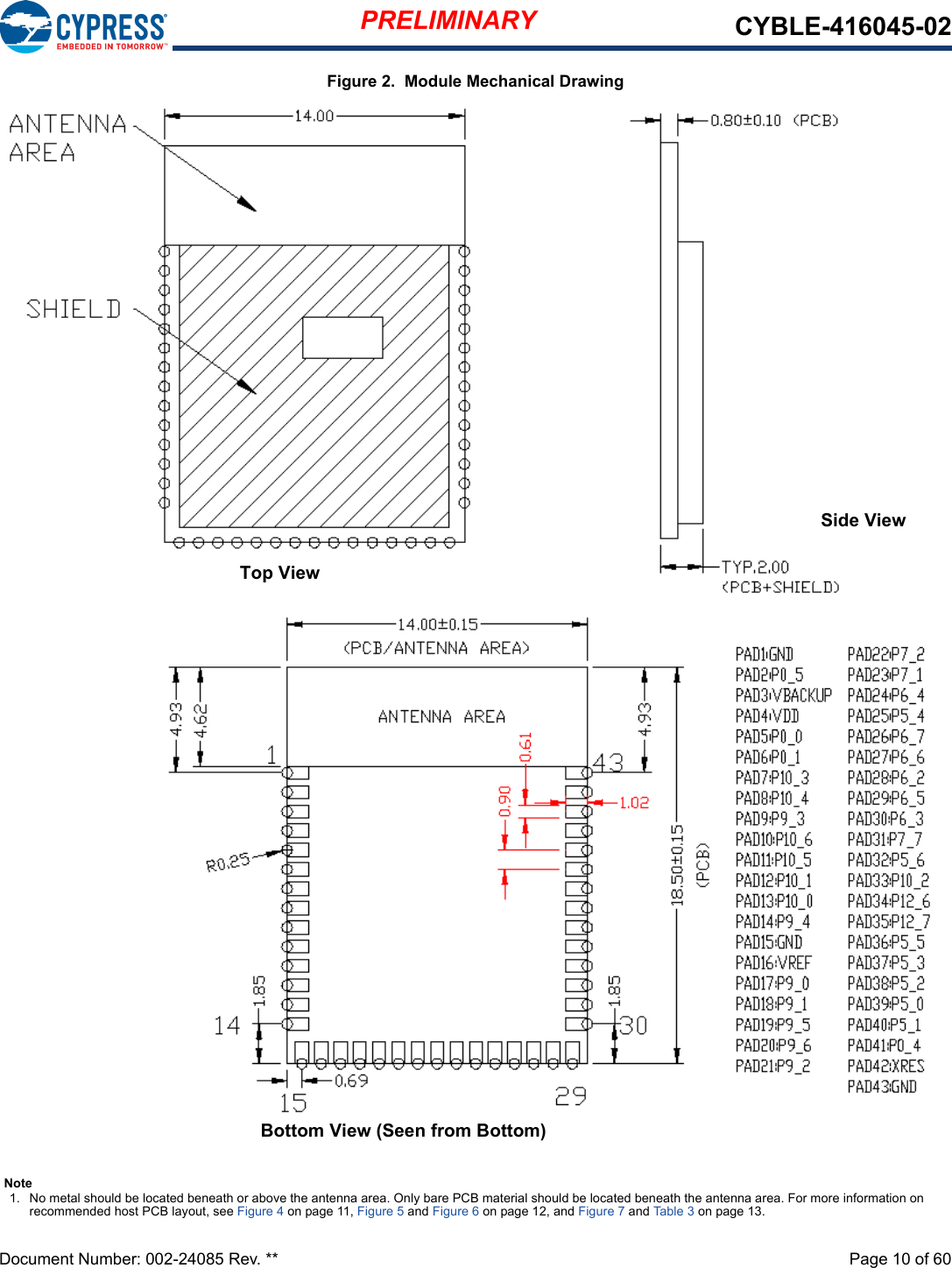
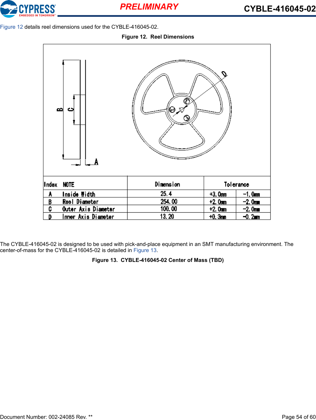
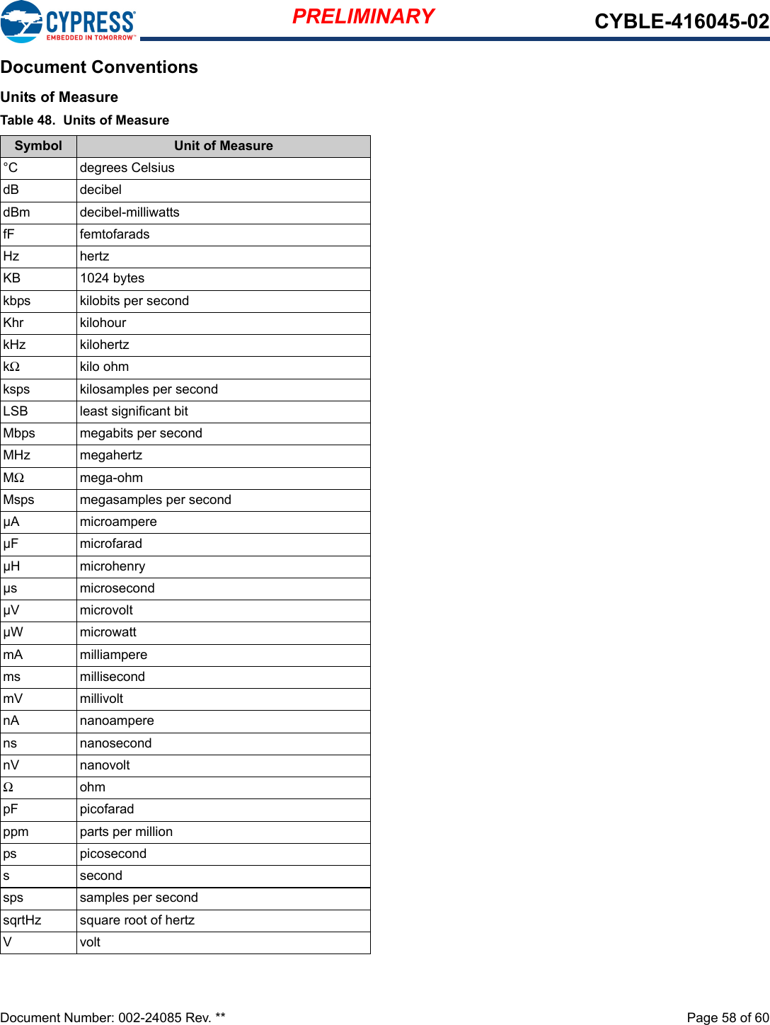
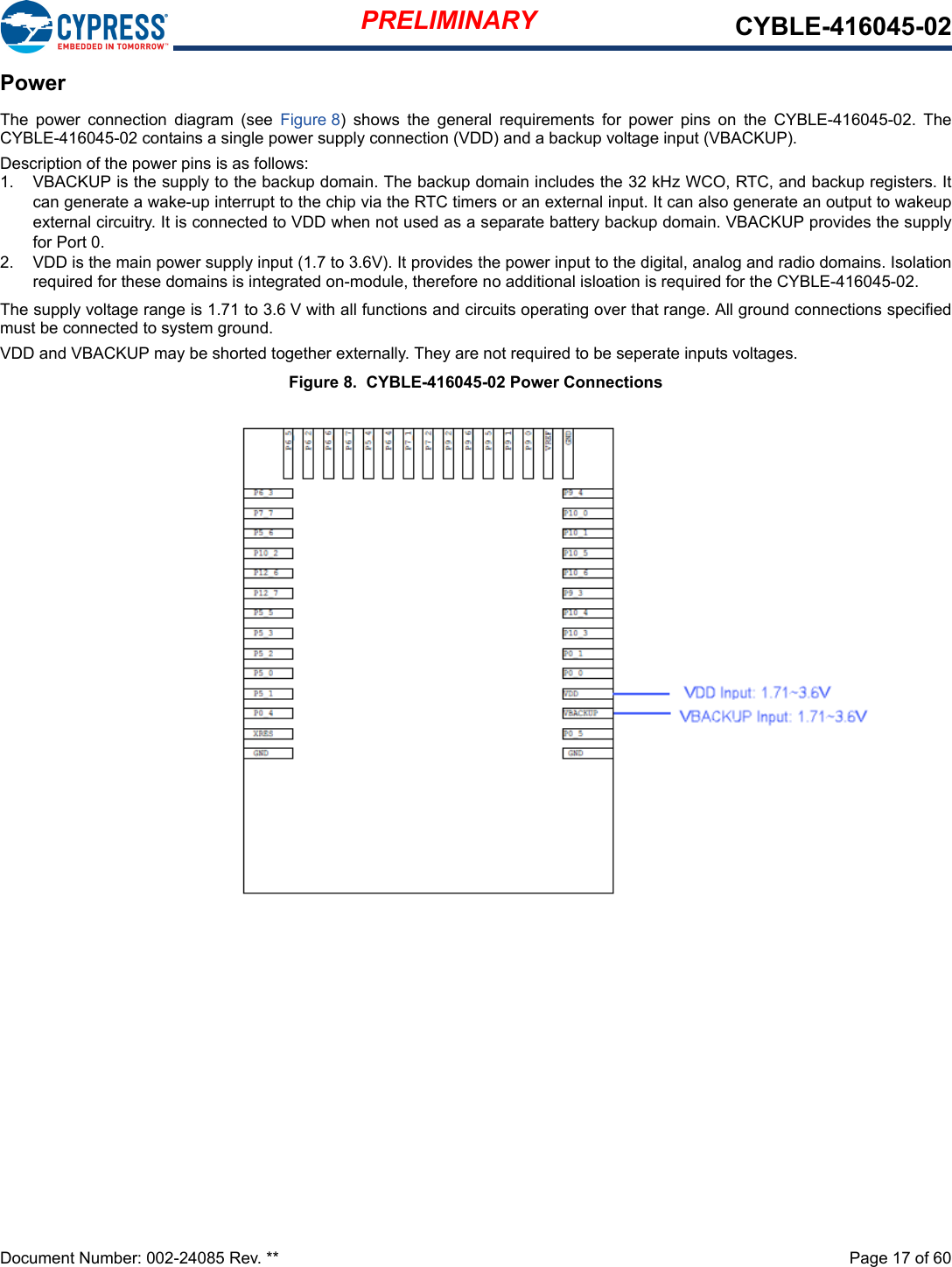
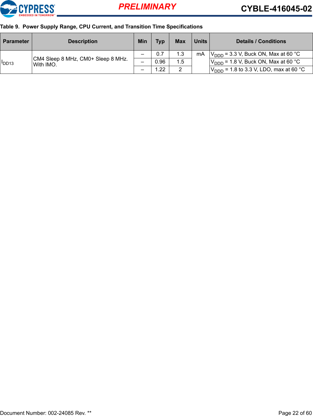
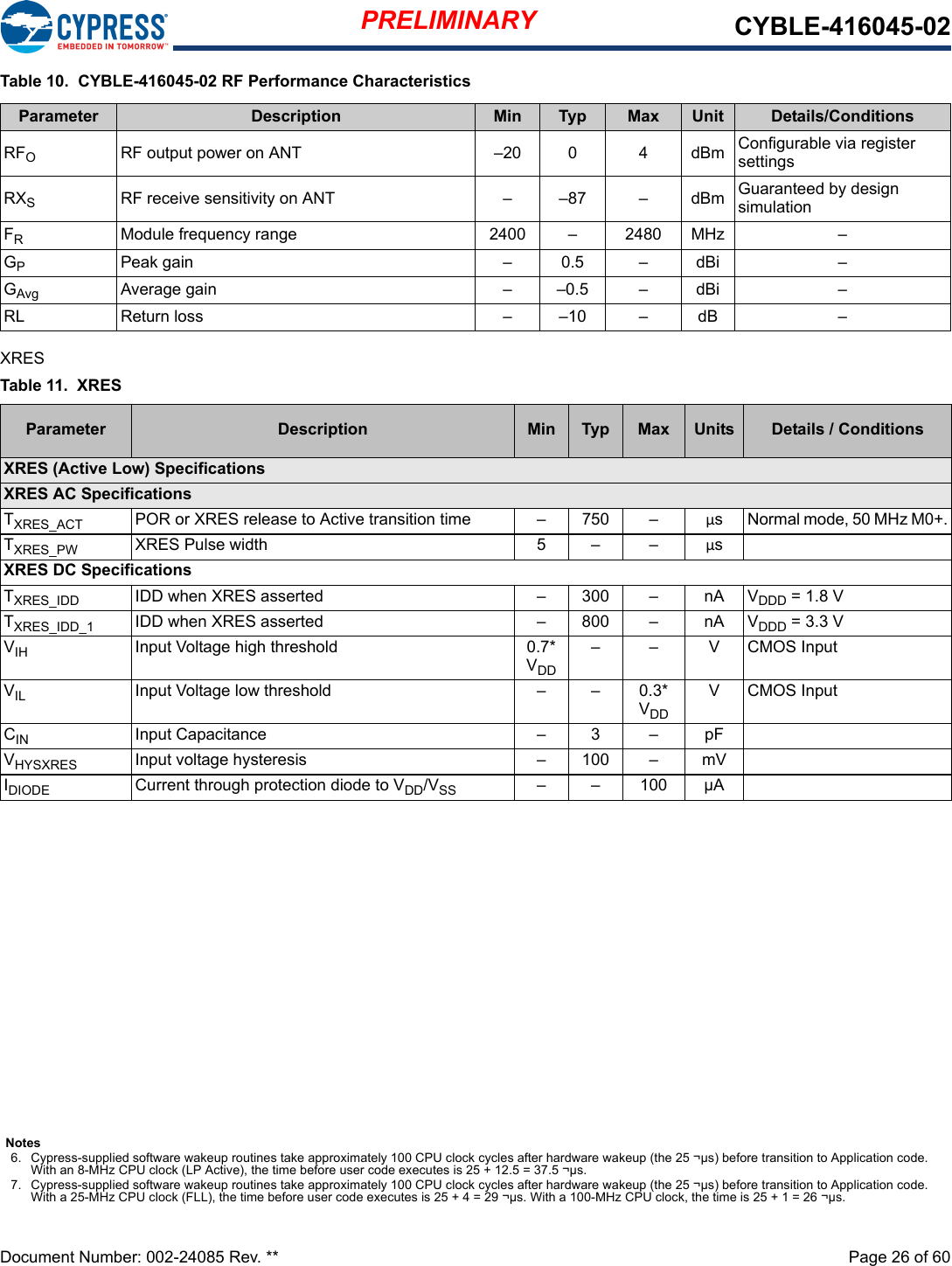
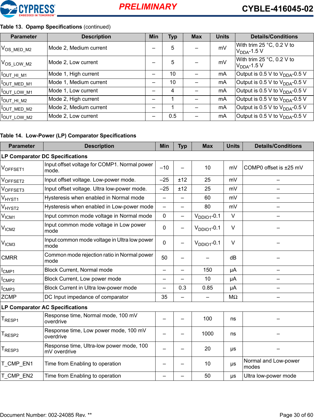
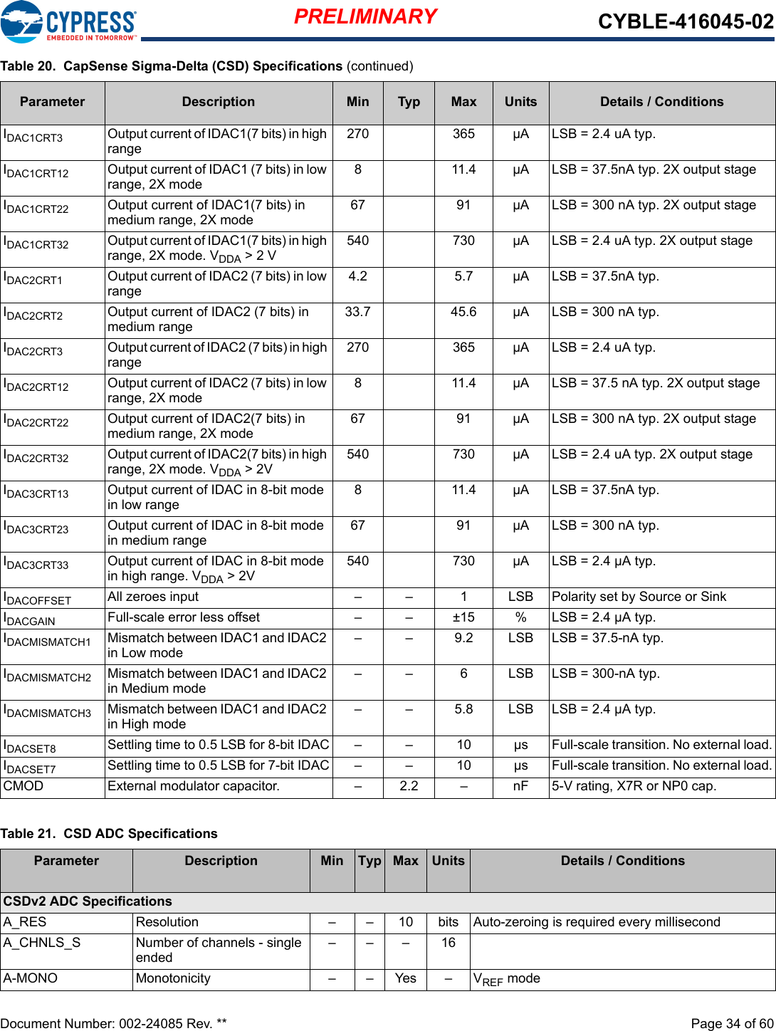
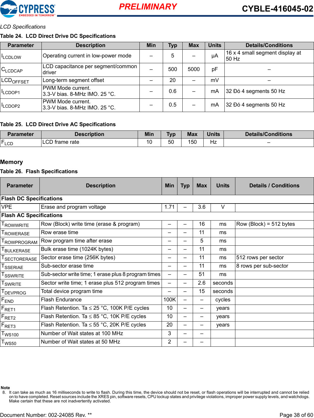
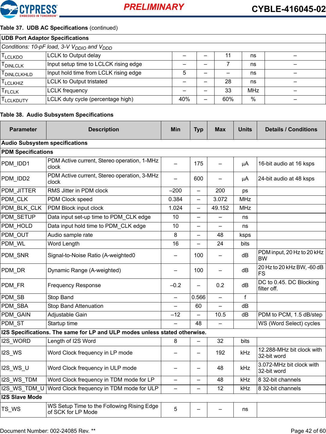
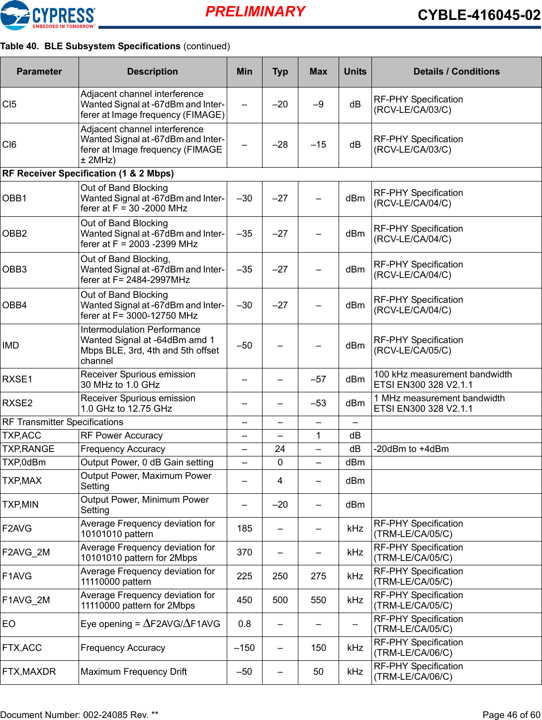
![PRELIMINARY CYBLE-416045-02Document Number: 002-24085 Rev. ** Page 14 of 60Digital and Analog Capablities and ConnectionsTable 4 and Ta ble 5 detail the solder pad connection definitions and available functions for each connection pad. Table 4 lists the solder pads on CYBLE-416045-02, the BLE device port-pin, and denotes whether the digital function shown is available for each solder pad. Table 5 denotes whether the analog function shown is available for each solder pad. Each connection is configurable for a single option shown with a 3.Table 4. Digital Peripheral CapabilitiesPad NumberDevice Port Pin UART SPI I2CTCPWM[2,3] CapSenseEXT_CLK_IN AUDIO CMP Dig-ital Out SWD/JTAG GPIO1GND[4] Ground Connection2P0.53(scb0_CTS) 3(scb0_SS0) tcpwm[0].line_compl[2]tcpwm[1].line_compl[2]33 33 VBACKUP Battery Backup Domain Input Voltage (1.71 V to 3.6 V)4 VDD Power Supply Input Voltage (1.71 V to 3.6 V)5P0.0 3(scb0_SS1) tcpwm[0].line[0]tcpwm[1].line[0]33 36P0.1 3(scb0_SS2) tcpwm[0].line_compl[0]tcpwm[1].line_compl[0]33(JTAG RST) 37 P10.3 3(scb1_CTS) 3(scb1_SS0) tcpwm[0].line_compl[7]tcpwm[1].line_compl[23]338 P10.4 3(scb1_SS1) tcpwm[0].line[0]tcpwm[1].line[0]33PDM_CLK 39P9.33(scb2_CTS) 3(scb2_SS0) tcpwm[0].line_compl[5]tcpwm[1].line_compl[21]3ctb_cmp1 310 P10.6 3(scb1_SS3) tcpwm[0].line[1]tcpwm[1].line[2]3311 P10.5 3(scb1_SS2) tcpwm[0].line_compl[0]tcpwm[1].line_compl[0]33PDM_DATA 312 P10.1 3(scb1_TX) 3(scb1_MISO) 3(scb1_SDA) tcpwm[0].line_compl[6]tcpwm[1].line_compl[22]3313 P10.0 3(scb1_RX) 3(scb1_MOSI) 3(scb1_SCL) tcpwm[0].line[6]tcpwm[1].line[22]3314 P9.4 3(scb2_SS1) tcpwm[0].line[7]tcpwm[1].line[0]3315 GND Ground Connection16 VREF Voltage Reference Input (Optional)17 P9.0 3(scb2_RX) 3(scb2_MOSI) 3(scb2_SCL) tcpwm[0].line[4]tcpwm[1].line[20]3318 P9.1 3(scb2_TX) 3(scb2_MISO) 3(scb2_SDA) tcpwm[0].line_compl[4]tcpwm[1].line_compl[20]3319 P9.5 3(scb2_SS2) tcpwm[0].line_compl[7]tcpwm[1].line_compl[0]3320 P9.6 3(scb2_SS3) tcpwm[0].line[0]tcpwm[1].line[1]3321 P9.2 3(scb2_RTS) 3(scb2_SCLK) tcpwm[0].line[5]tcpwm[1].line[21]3ctb_cmp0 322 P7.2 3(scb4_RTS) 3(scb4_SCLK) tcpwm[0].line[5]tcpwm[1].line[13]3323 P7.1 3(scb4_TX) 3(scb4_MISO) 3(scb4_SDA) tcpwm[0].line_compl[4]tcpwm[1].line_compl[12]3324 P6.4 3(SCB6_RX) 3(scb6_MOSI)(scb8_MOSI)3(scb8_SCL)(scb6_SCL) tcpwm[0].line[2]tcpwm[1].line[10]33(JTAG TDO) 325 P5.4 3(scb5_SS1) tcpwm[0].line[6]tcpwm[1].line[6]33I2S_SCK_RX 326 P6.7 3(scb6_CTS) 3(scb6_SS0)(scb8_SS0) tcpwm[0].line_compl[3]tcpwm[1].line_compl[1133(SWDCLK)(JTAG TCLK)327 P6.6 3(scb6_RTS) 3(scb6_SCLK)(scb8_SCLK) tcpwm[0].line[3]tcpwm[1].line[11]33(SWDIO)(JTAG TMS)328 P6.2 3(scb3_RTS) 3(scb3_SCLK)(scb8_SCLK) tcpwm[0].line[1]tcpwm[1].line[9]3329 P6.5 3(scb6_TX) 3(scb6_MISO)(scb8_MISO)3(scb8_SDA)3(scb6_SDA) tcpwm[0].line_compl[2]tcpwm[1].line_compl[10]33(JTAG TDI) 3](https://usermanual.wiki/Cypress-Semiconductor/6045/User-Guide-3880583-Page-14.png)
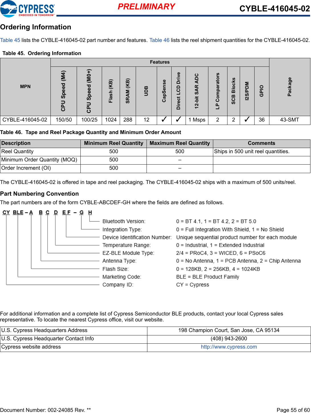
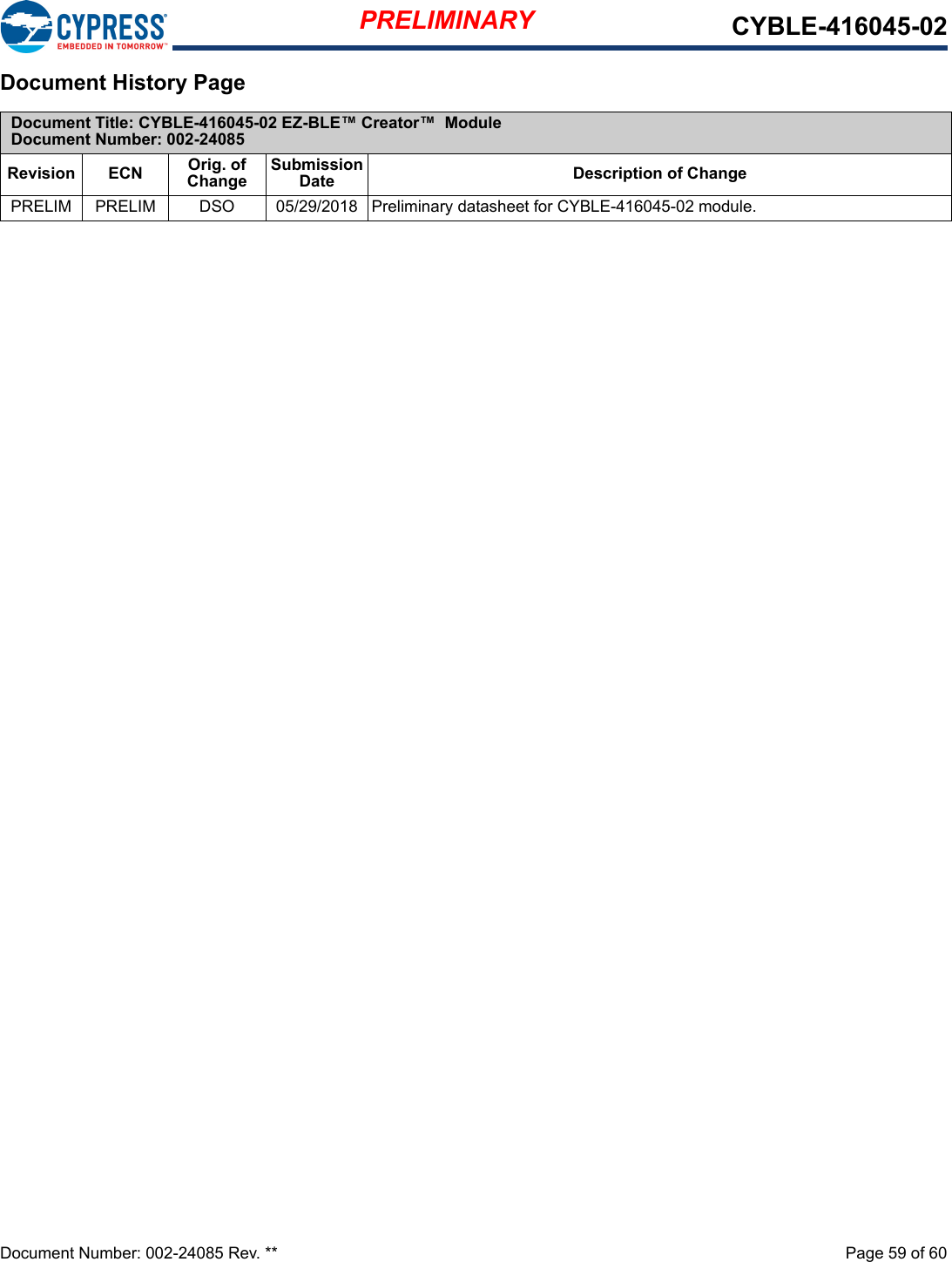
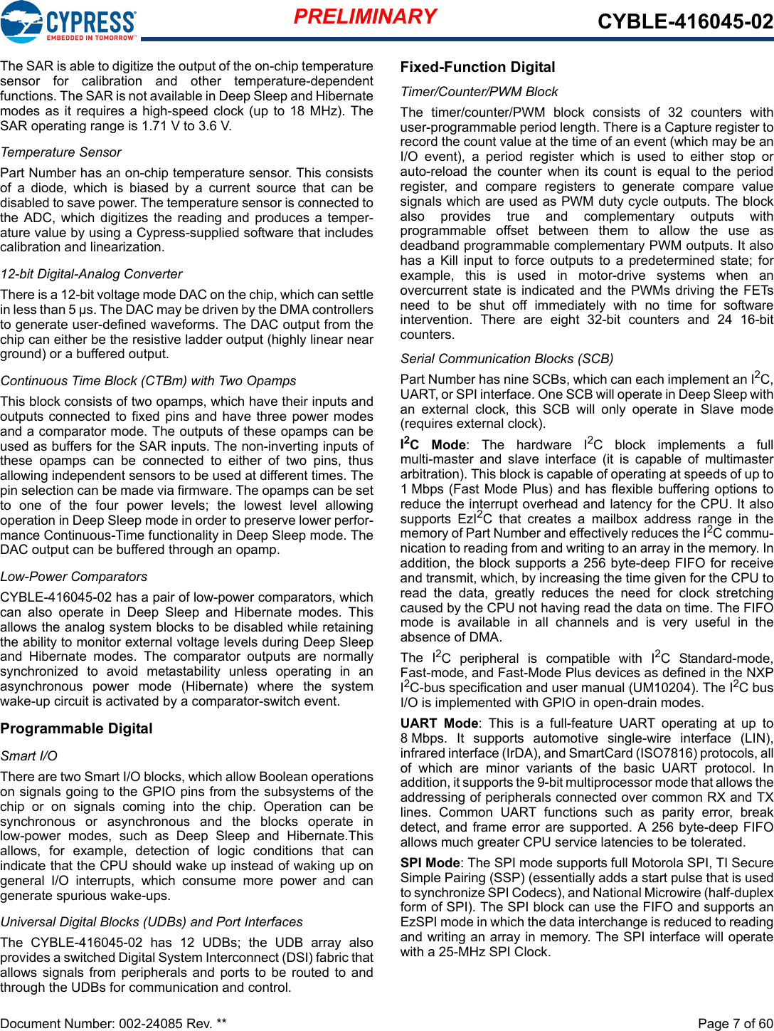
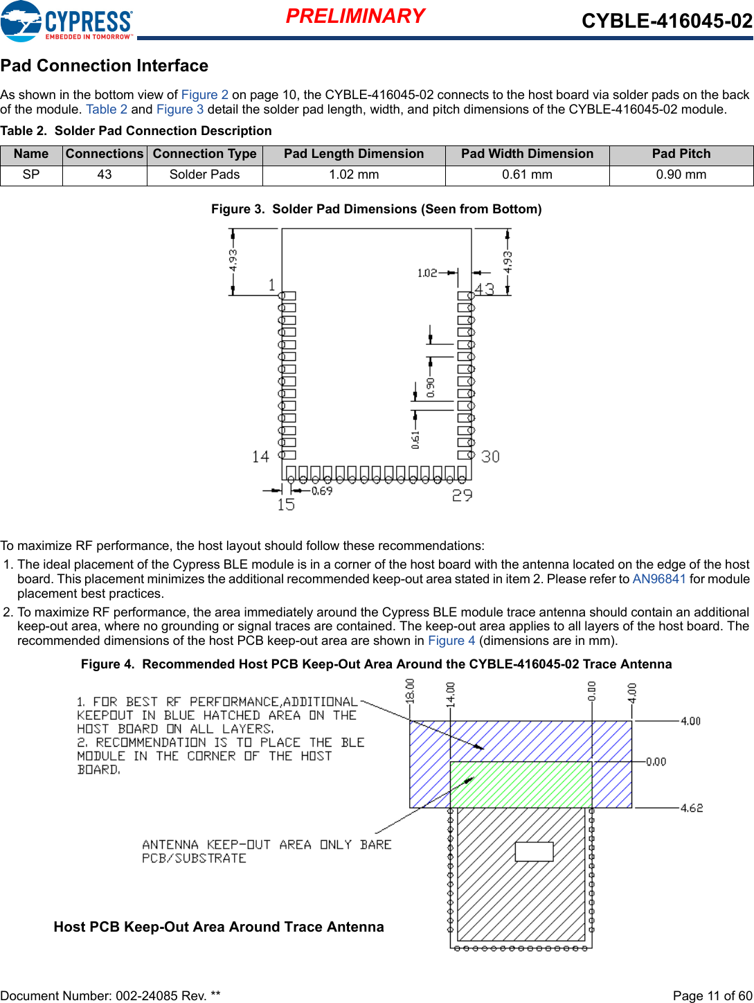
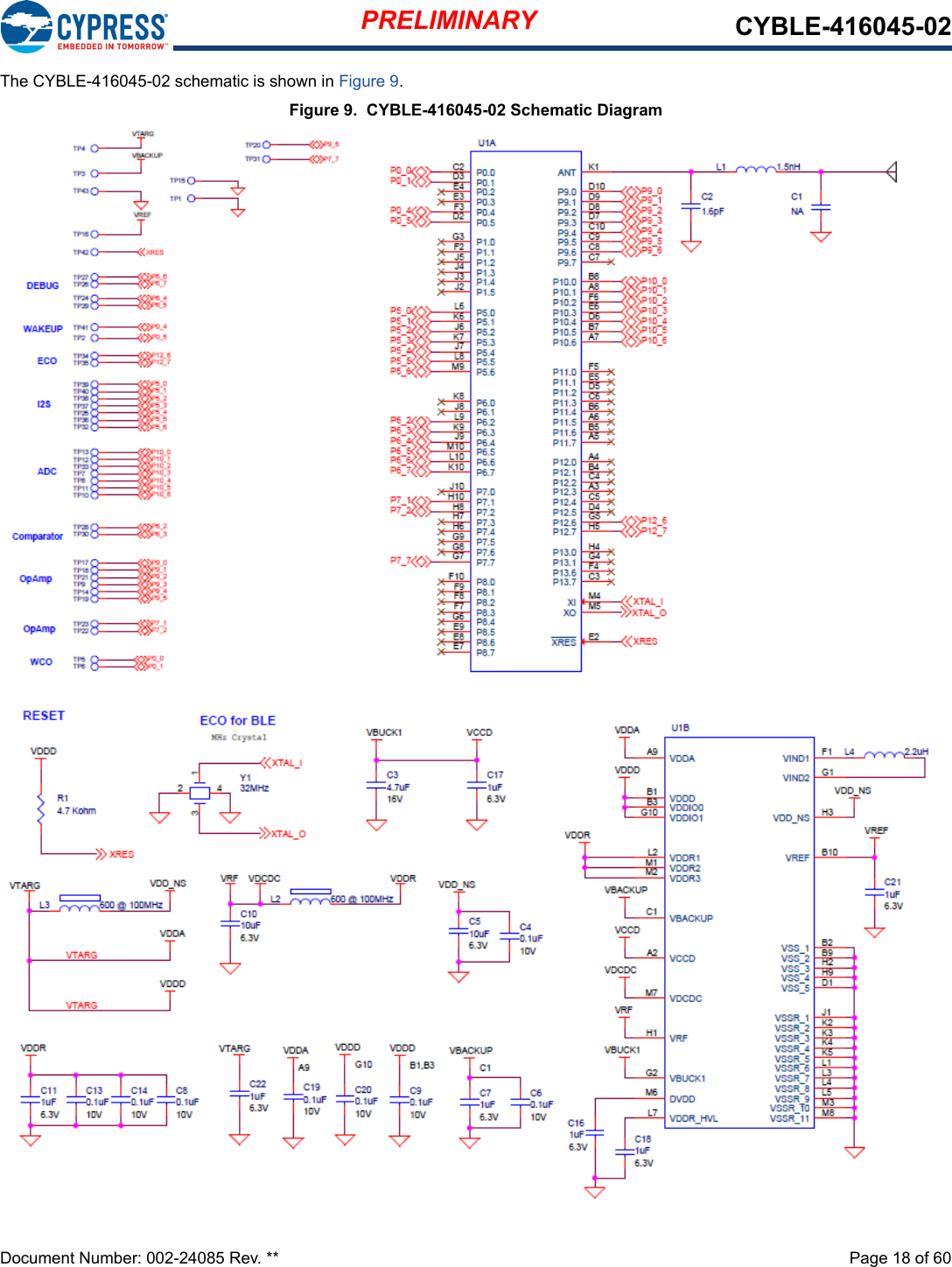
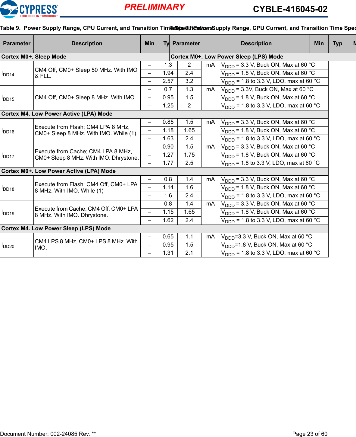
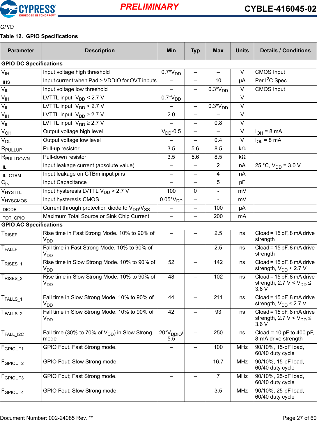
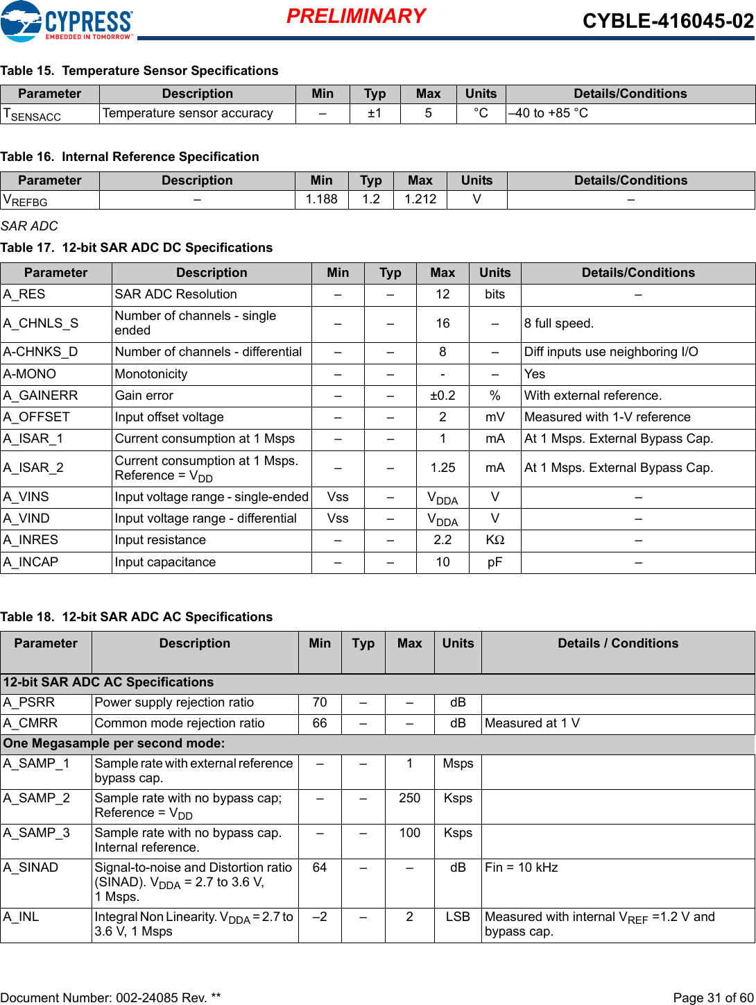
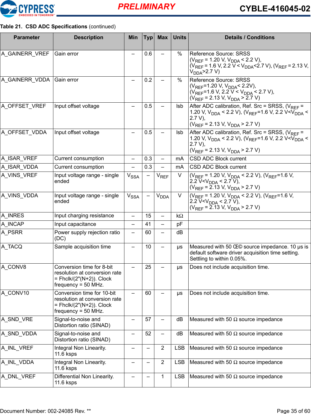
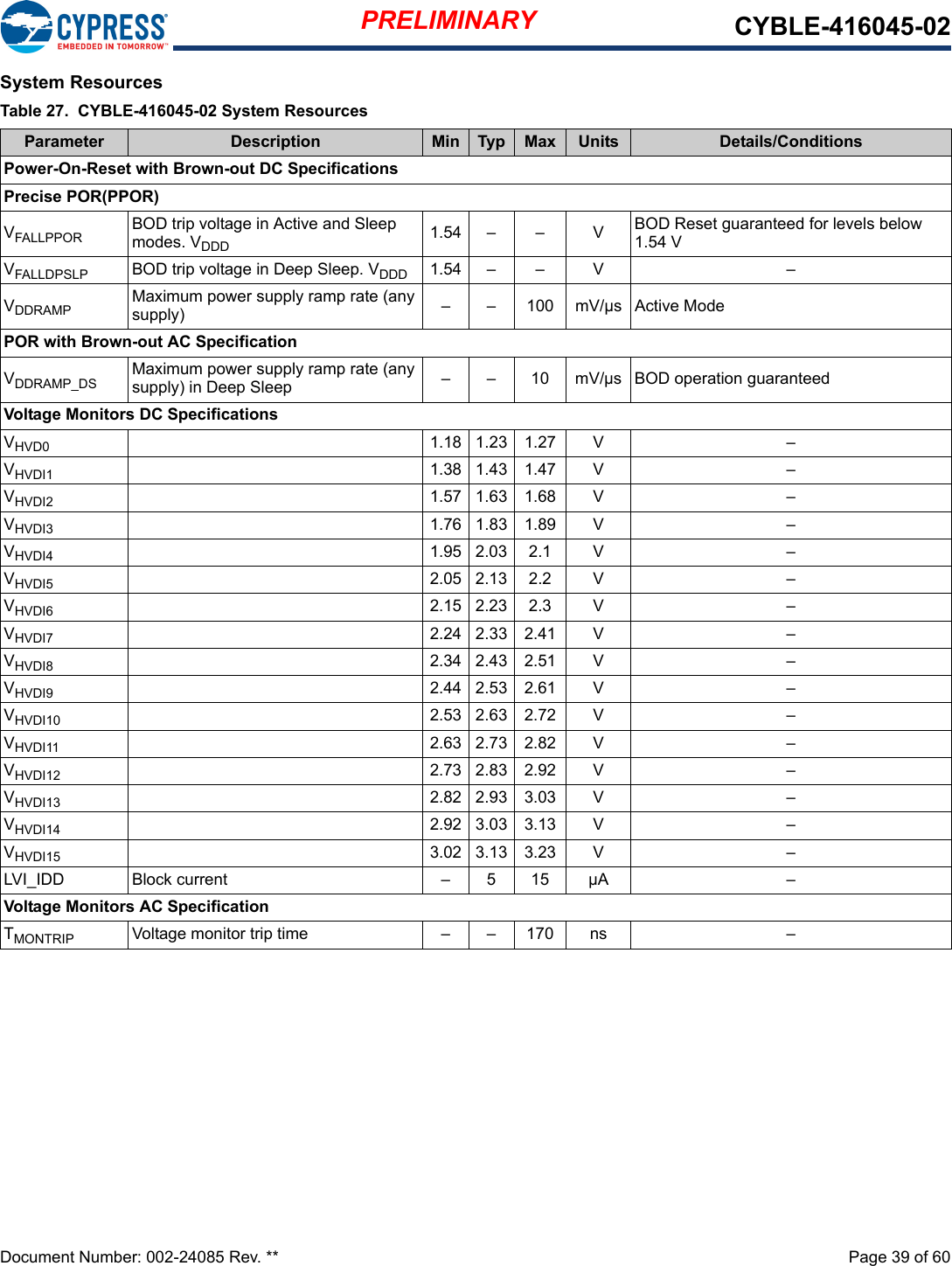
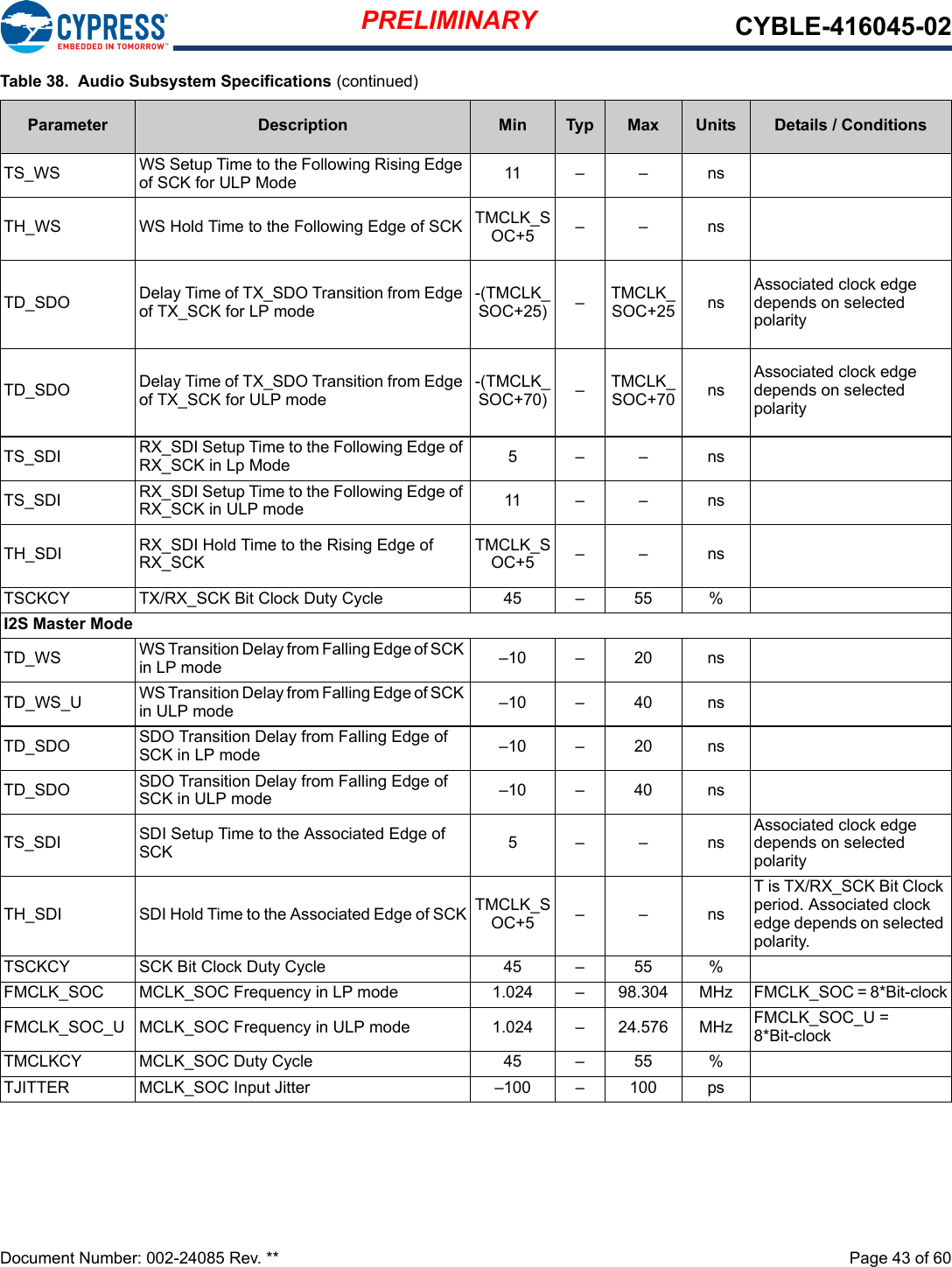
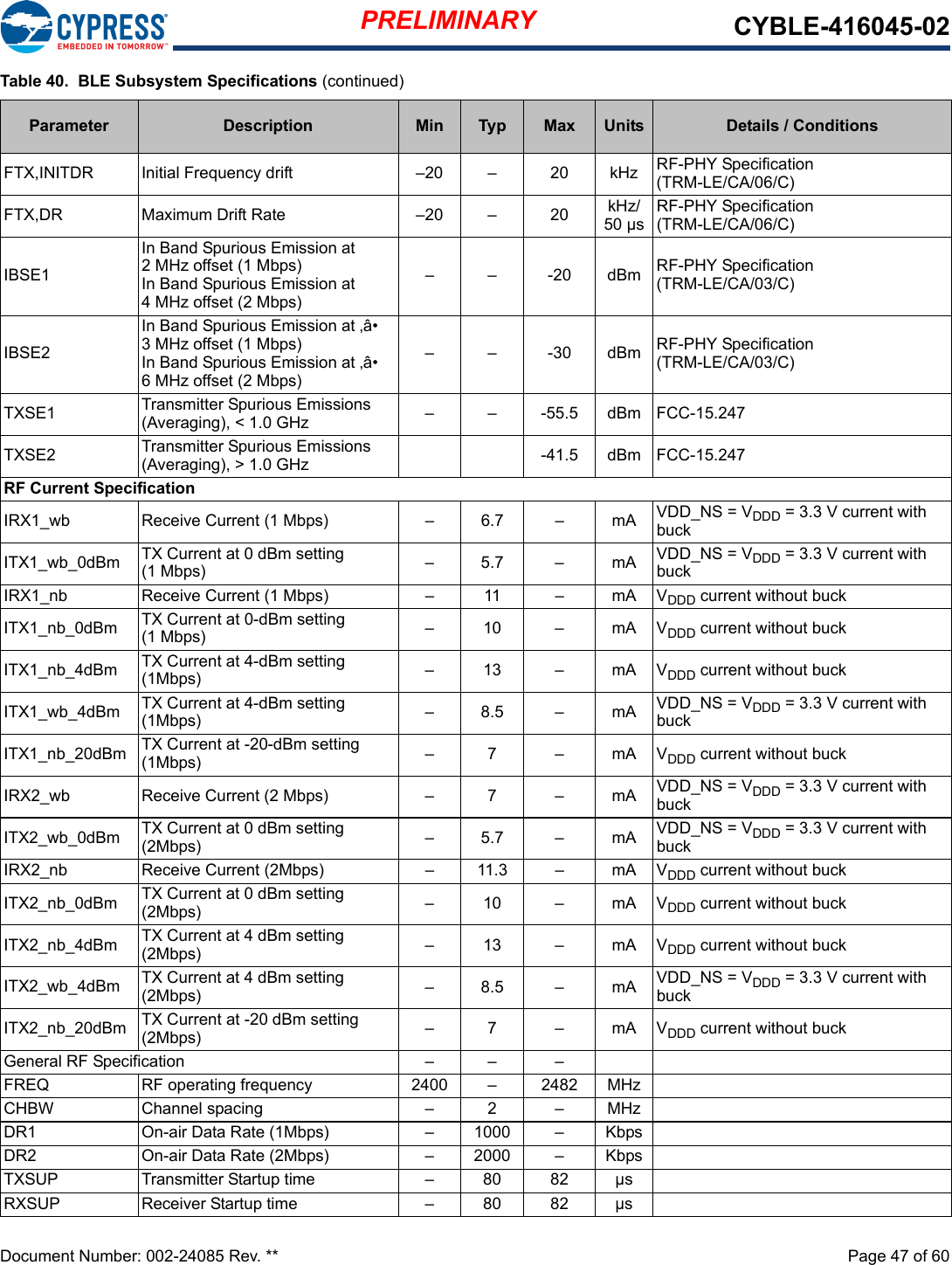
![PRELIMINARY CYBLE-416045-02Document Number: 002-24085 Rev. ** Page 15 of 6030 P6.3 3(scb3_CTS) 3(scb3_SS0)(scb8_SS0) tcpwm[0].line_compl[1]tcpwm[1].line_compl[9]3331 P7.7 3(scb3_SS1) tcpwm[0].line_compl[7]tcpwm[1].line_compl[15]3332 P5.6 3(scb5_SS3) tcpwm[0].line[7]tcpwm[1].line[7]33I2S_SDI_RX 333 P10.2 3(scb1_RTS) 3(scb1_SCLK) tcpwm[0].line[7]tcpwm[1].line[23]3334 P12.6 3(scb6_SS3) tcpwm[0].line[7]tcpwm[1].line[7]3335 P12.7 tcpwm[0].line_compl[7]tcpwm[1].line_compl[7]3336 P5.5 3(scb5_SS2) tcpwm[0].line_compl[6]tcpwm[1].line_compl[6]33I2S_WS_RX 337 P5.3 3(scb5_CTS) 3(scb5_SS0) cpwm[0].line_compl[5]tcpwm[1].line_compl[5]33I2S_SDO_TX 338 P5.2 3(scb5_RTS) 3(scb5_SCLK) tcpwm[0].line[5]tcpwm[1].line[5]33I2S_WS_TX 339 P5.0 3(scb5_RX) 3(scb5_MOSI) 3(scb5_SCL) tcpwm[0].line[4]tcpwm[1].line[4]33I2S_EXT_CLK 340 P5.1 3(scb5_TX) 3(scb5_MISO) 3(scb5_SDA) tcpwm[0].line_compl[4]tcpwm[1].line_compl[4]33I2S_CLK_TX 341 P0.4 3(scb0_RTS) 3(scb0_SCLK) tcpwm[0].line[2]tcpwm[1].line[2]3342 XRES External Reset (Active Low)43 GND[4] Ground ConnectionTable 4. Digital Peripheral CapabilitiesNotes2. TCPWM stands for timer, counter, and PWM. If supported, the pad can be configured to any of these peripheral functions.3. TCPWM connections on ports 0, 1, 2, and 3 can be routed through the Digital Signal Interconnect (DSI) to any of the TCPWM blocks and can be either positive or negative polarity.4. The main board needs to connect both GND connections (Pad 1 and Pad 32) on the module to the common ground of the system.](https://usermanual.wiki/Cypress-Semiconductor/6045/User-Guide-3880583-Page-15.png)
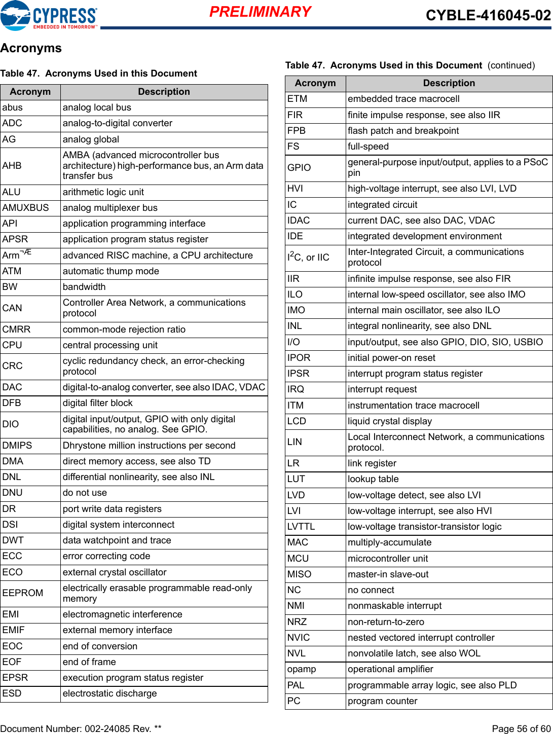
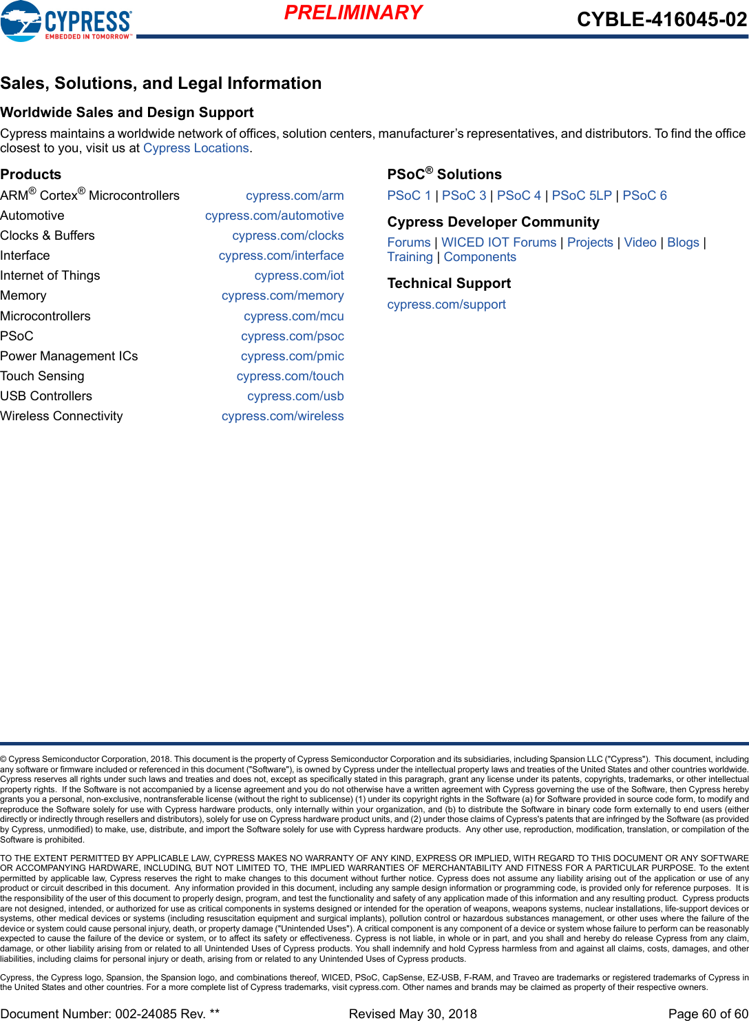
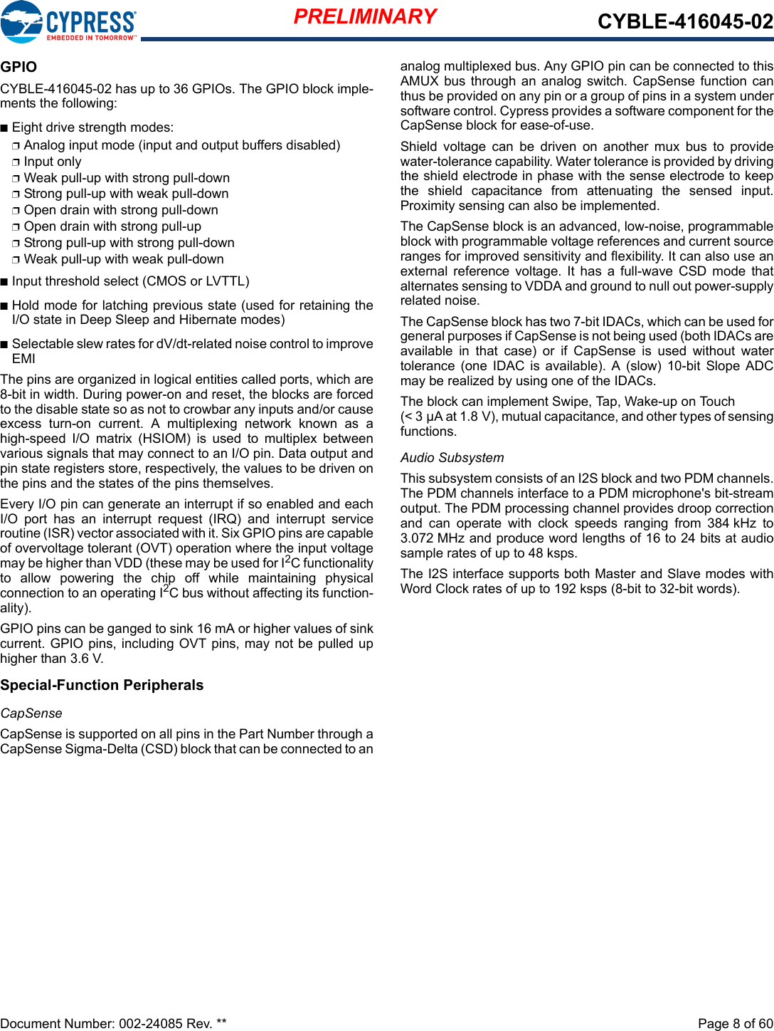
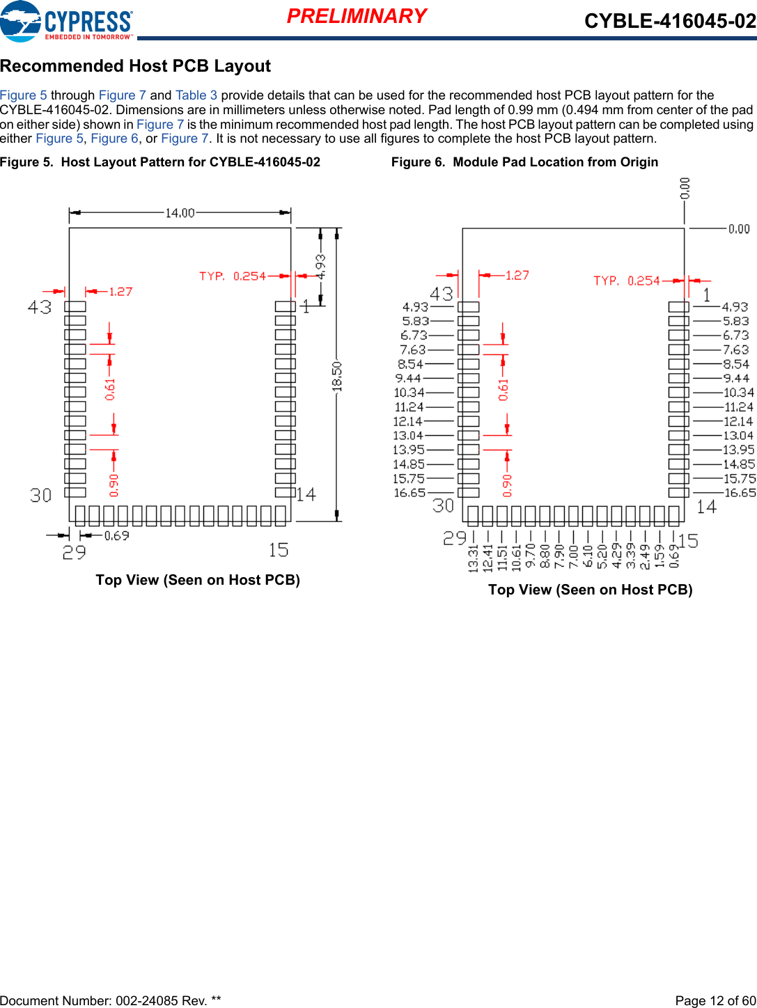
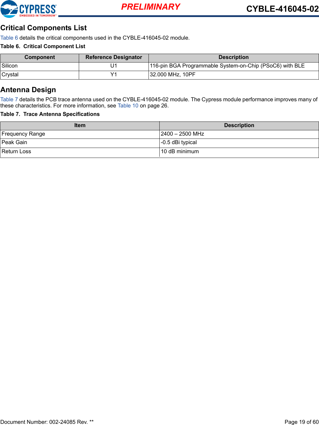
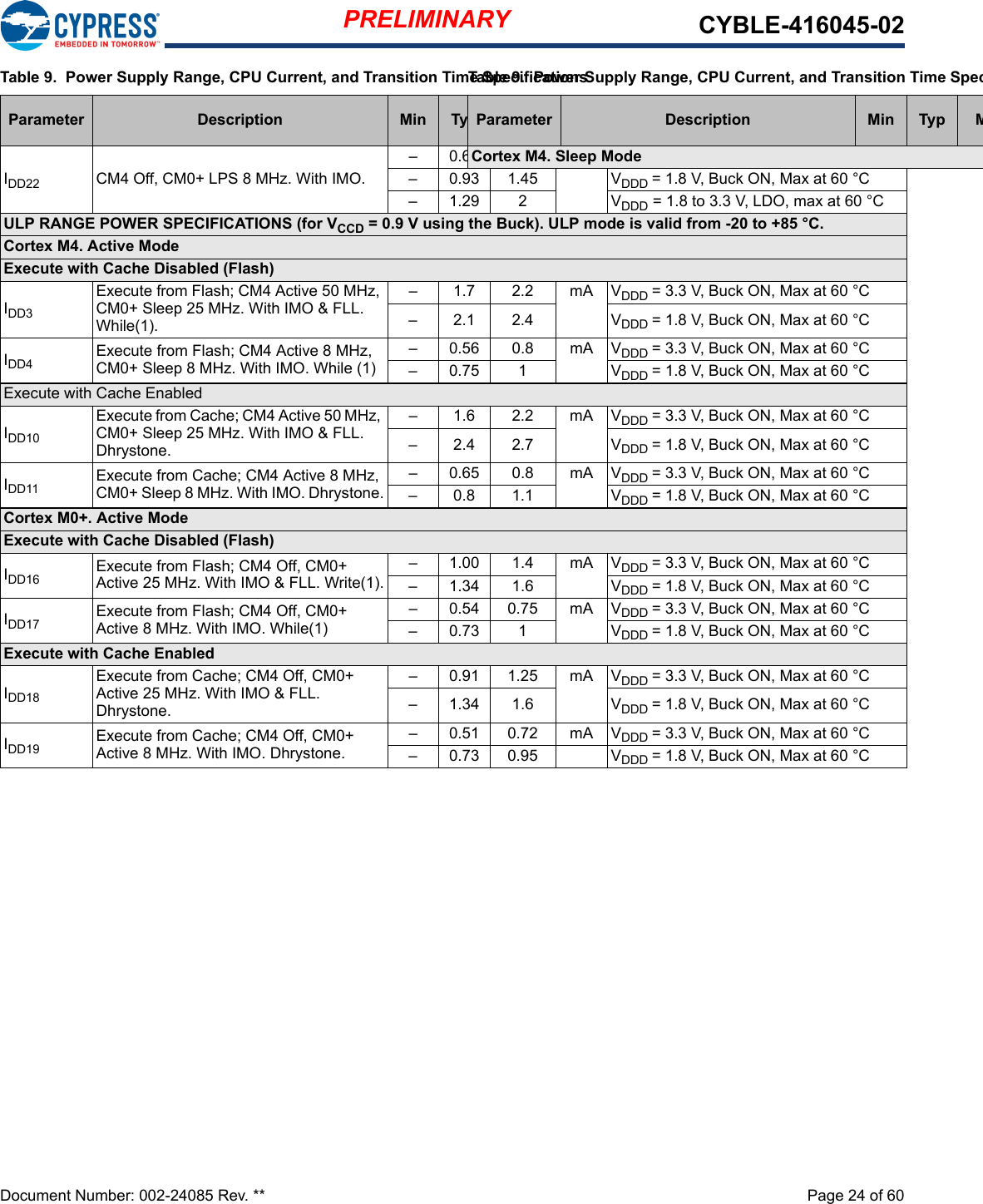
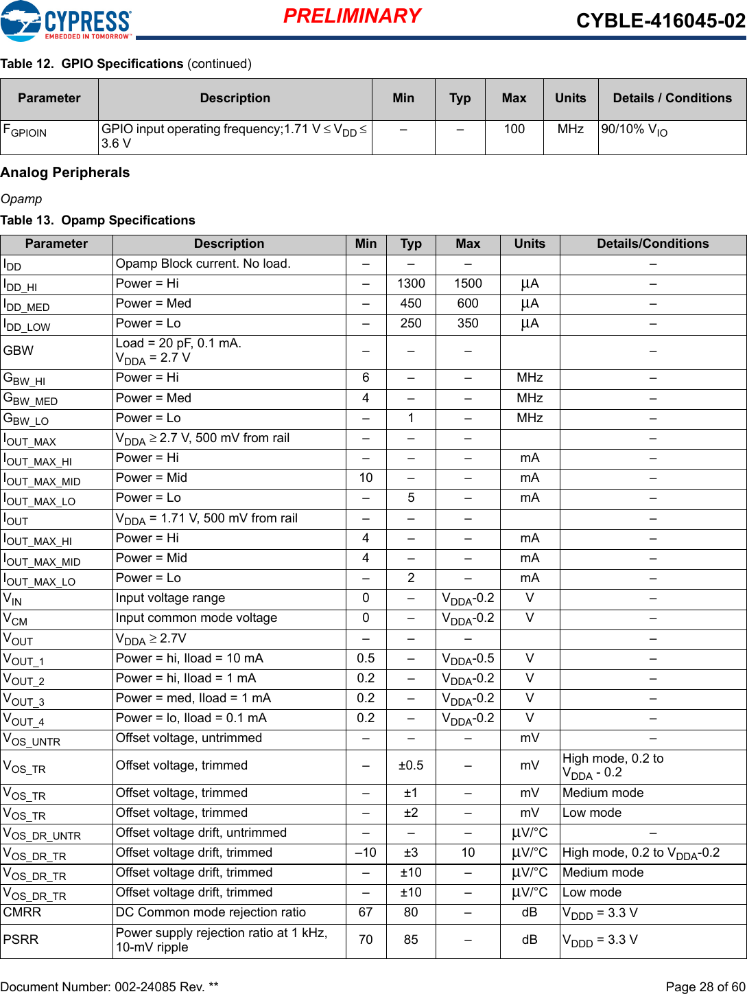
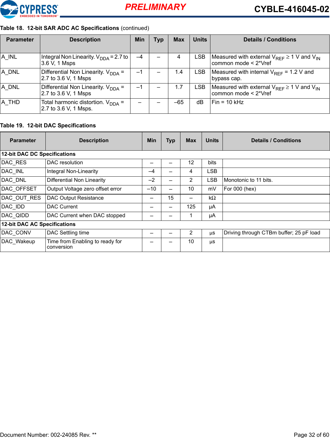
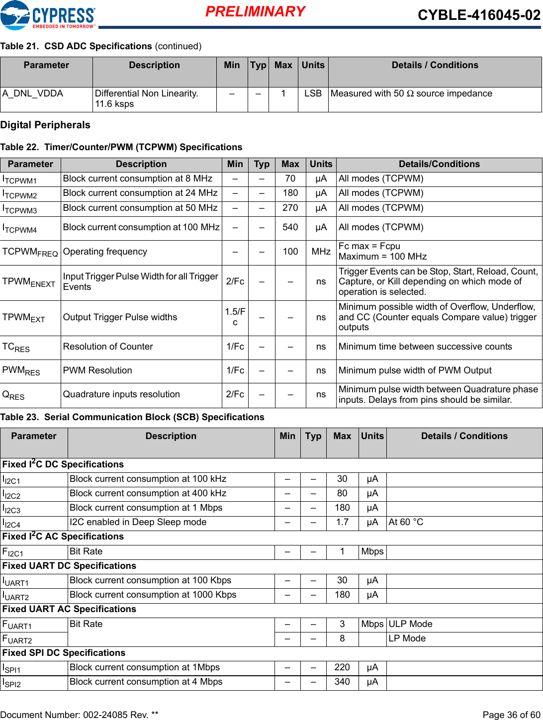
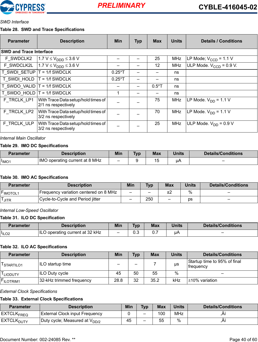
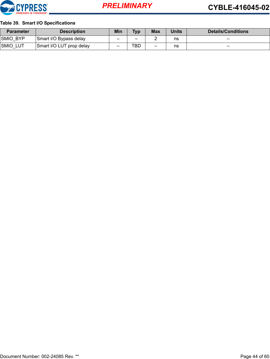
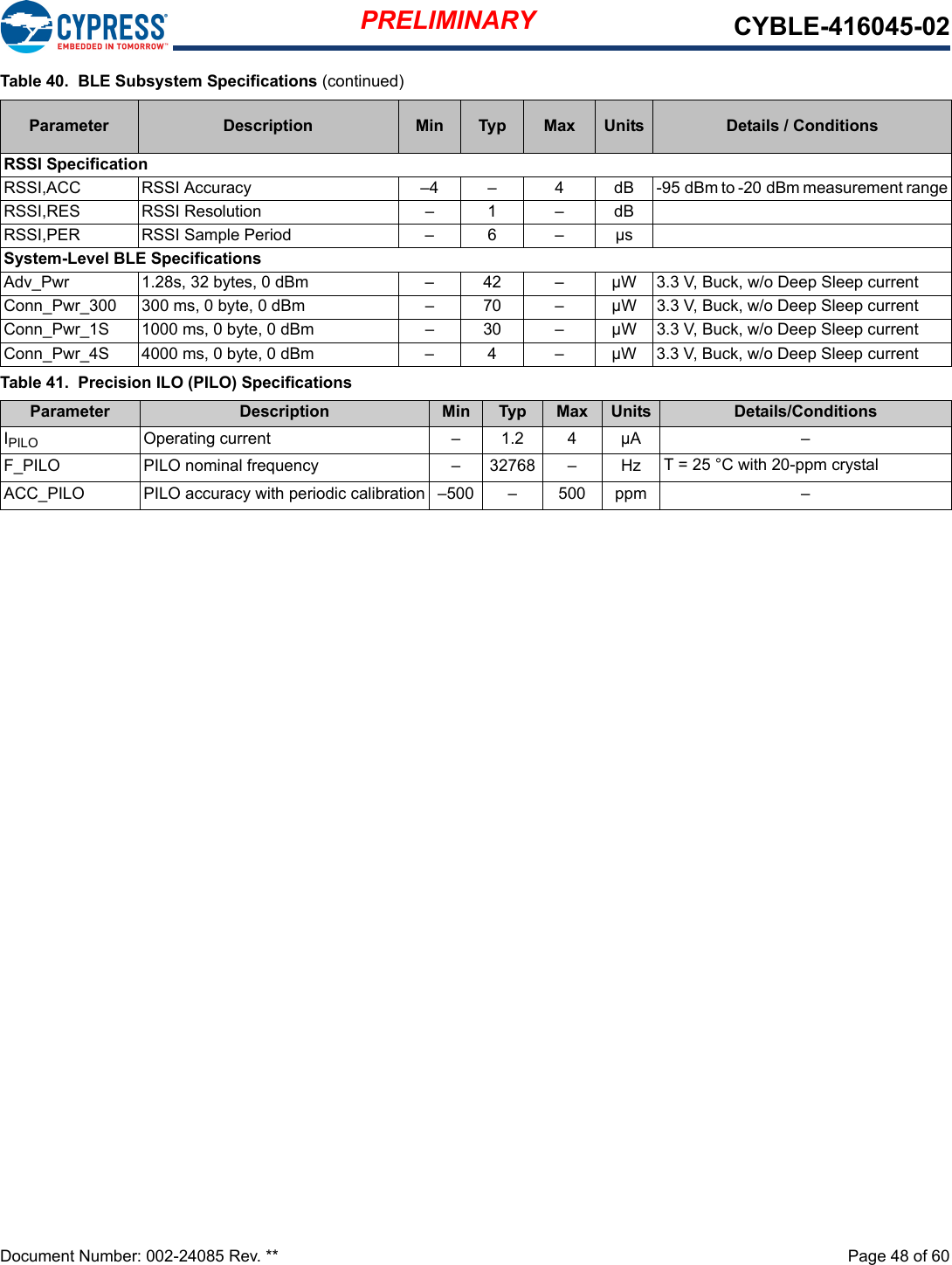
![PRELIMINARY CYBLE-416045-02Document Number: 002-24085 Rev. ** Page 16 of 60Table 5. Additional Analog and Digital Functional CapabilitiesPad Number Device Port Pin Analog Functionality Digital HV Universal Digital Block (UDB) SMARTIO1 GND Ground Connection2P0.5 3(pmic_wakeup_out) 3(UDB0[5])3 VBACKUP Battery Backup Domain Input Voltage (1.71 V to 3.6 V)4 VDD Power Supply Input Voltage (1.71 V to 3.6 V)5P0.0 wco_in 3(UDB0[0])6 P0.1 wco_out 3(UDB0[1])7 P10.3 sarmux[3] 3(UDB9[3])8 P10.4 sarmux[4] 3(UDB9[4])9 P9.3 ctb_oa1_out 3(UDB10[3]) SMARTIO10[3]10 P10.6 sarmux[6] 3(UDB9[6])11 P10.5 sarmux[5] 3(UDB9[5])12 P10.1 sarmux[1] 3(UDB9[1])13 P10.0 sarmux[0] 3(UDB9[0])14 P9.4 ctb_oa1- 3(UDB10[4]) SMARTIO9[4]15 GND Ground Connection16 VREF Reference Voltage Input (Optional)17 P9.0 ctb_oa0+ 3(UDB10[0]) SMARTIO9[0]18 P9.1 ctb_oa0- 3(UDB10[1]) SMARTIO9[1]19 P9.5 ctb_oa1+ 3(UDB10[5]) SMARTIO9[5]20 P9.6 ctb_oa0+ 3(UDB10[6]) SMARTIO9[6]21 P9.2 ctb_oa0_out 3(UDB10[2]) SMARTIO9[2]22 P7.2 csd.csh_tankpaddcsd.csh_tankpads3(UDB5[2])23 P7.1 csd.cmodpaddcsd.cmodpads3(UDB5[1])24 P6.4 3(UDB4[4])25 P5.4 3(UDB3[5])26 P6.7 swd_clk 3(UDB4[7])27 P6.6 swd_data 3(UDB4[6])28 P6.2 lpcomp.inp_comp1 3(UDB4[2])29 P6.5 3(UDB4[5])30 P6.3 lpcomp.inn_comp1 3(UDB4[3])31 P7.7 csd.cshieldpads 3(UDB5[7])32 P5.6 lpcomp.inp_comp0 3(UDB3[6])33 P10.2 sarmux[2] 3(UDB9[2])34 P12.6 ECO_IN 3(UDB7[6])35 P12.7 ECO_OUT 3(UDB7[7])36 P5.5 3(UDB3[5])37 P5.3 3(UDB3[3])38 P5.2 3(UDB3[2])39 P5.0 3(UDB3[0])40 P5.1 3(UDB3[1])41 P0.4 pmic_wakeup_inhibernate_wakeup[1]3(UDB0[4])42 XRES External Reset (Active Low)43 GND Ground Connection](https://usermanual.wiki/Cypress-Semiconductor/6045/User-Guide-3880583-Page-16.png)
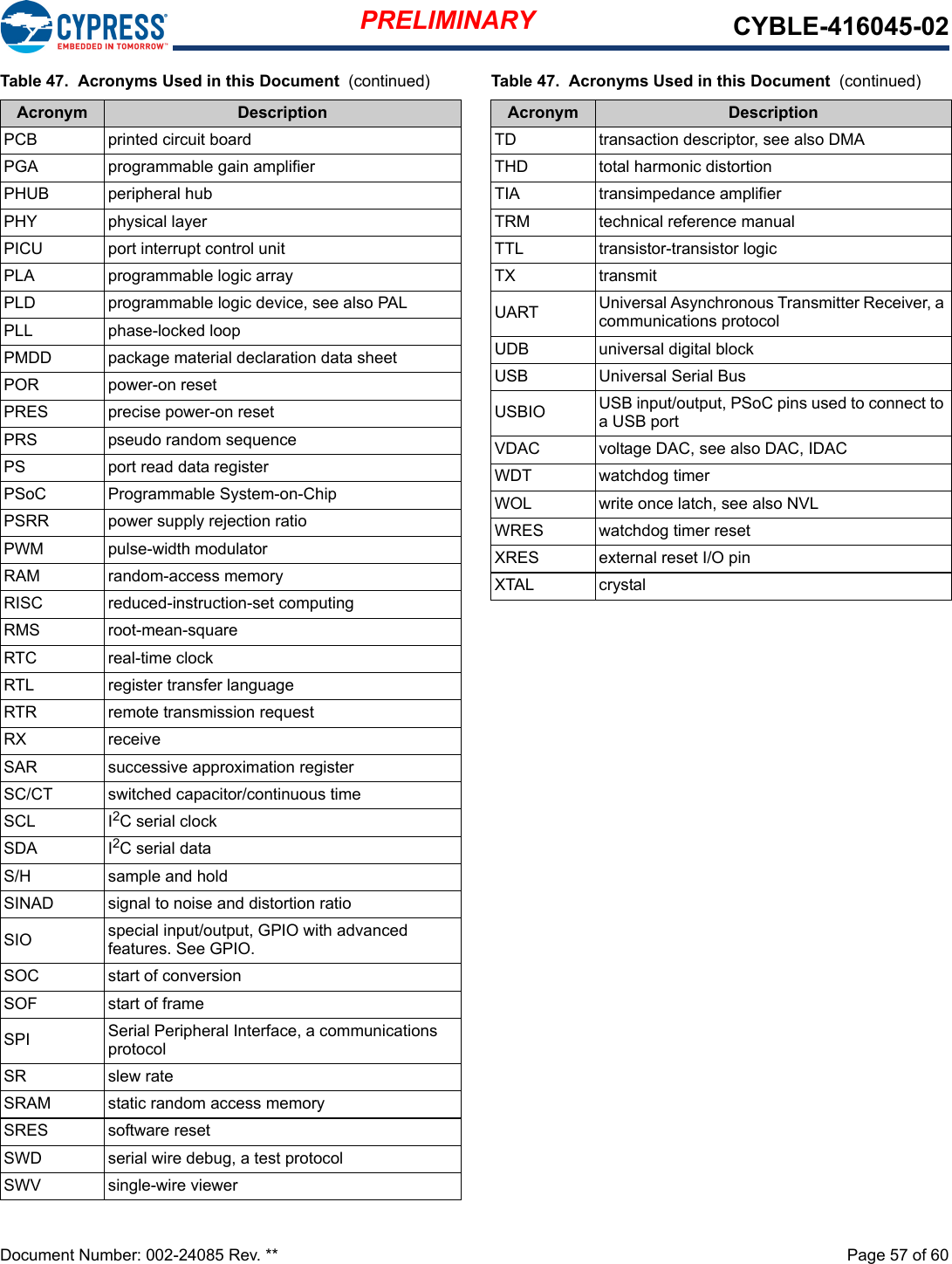
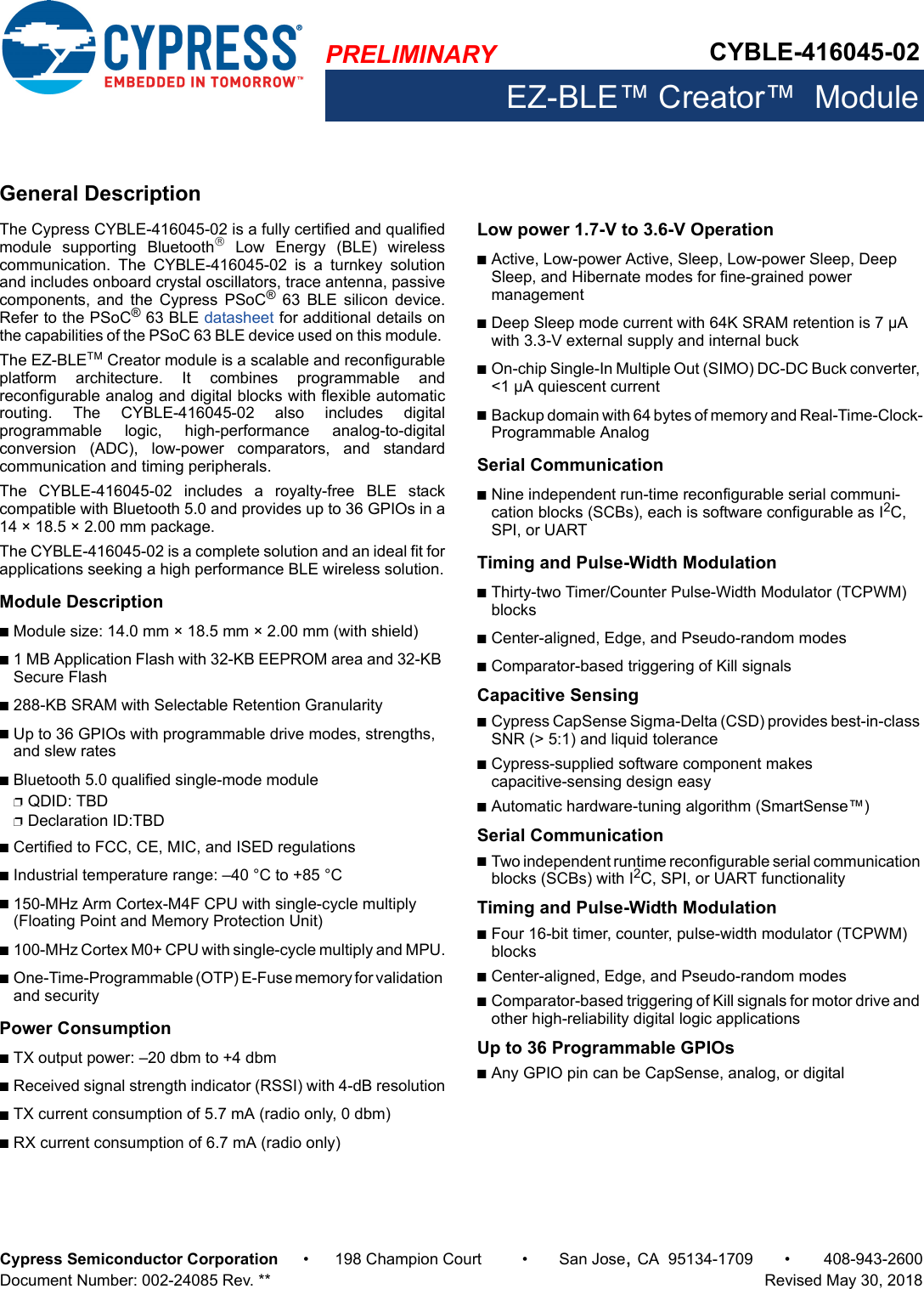
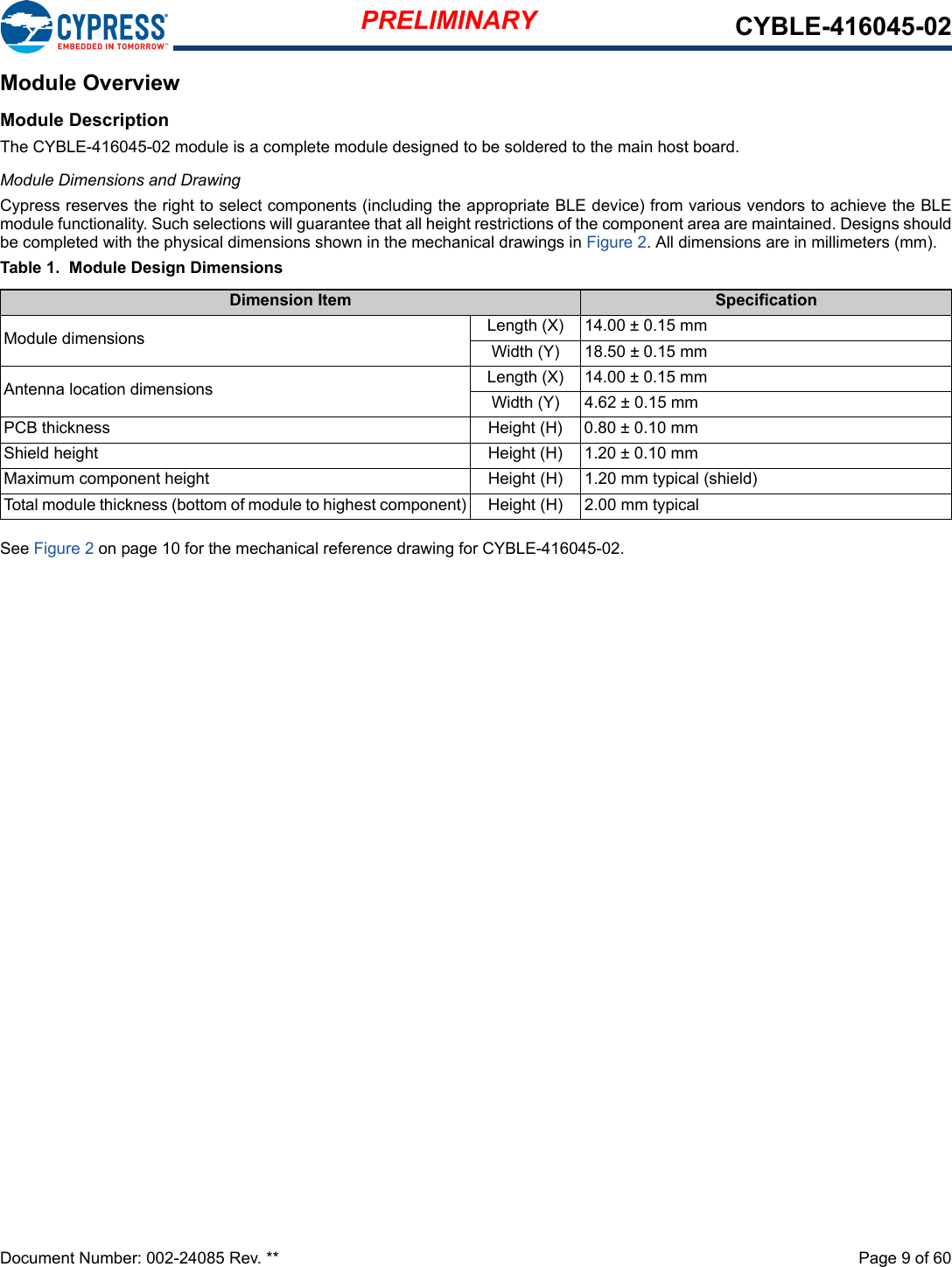
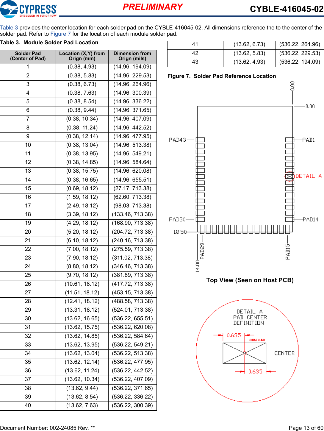
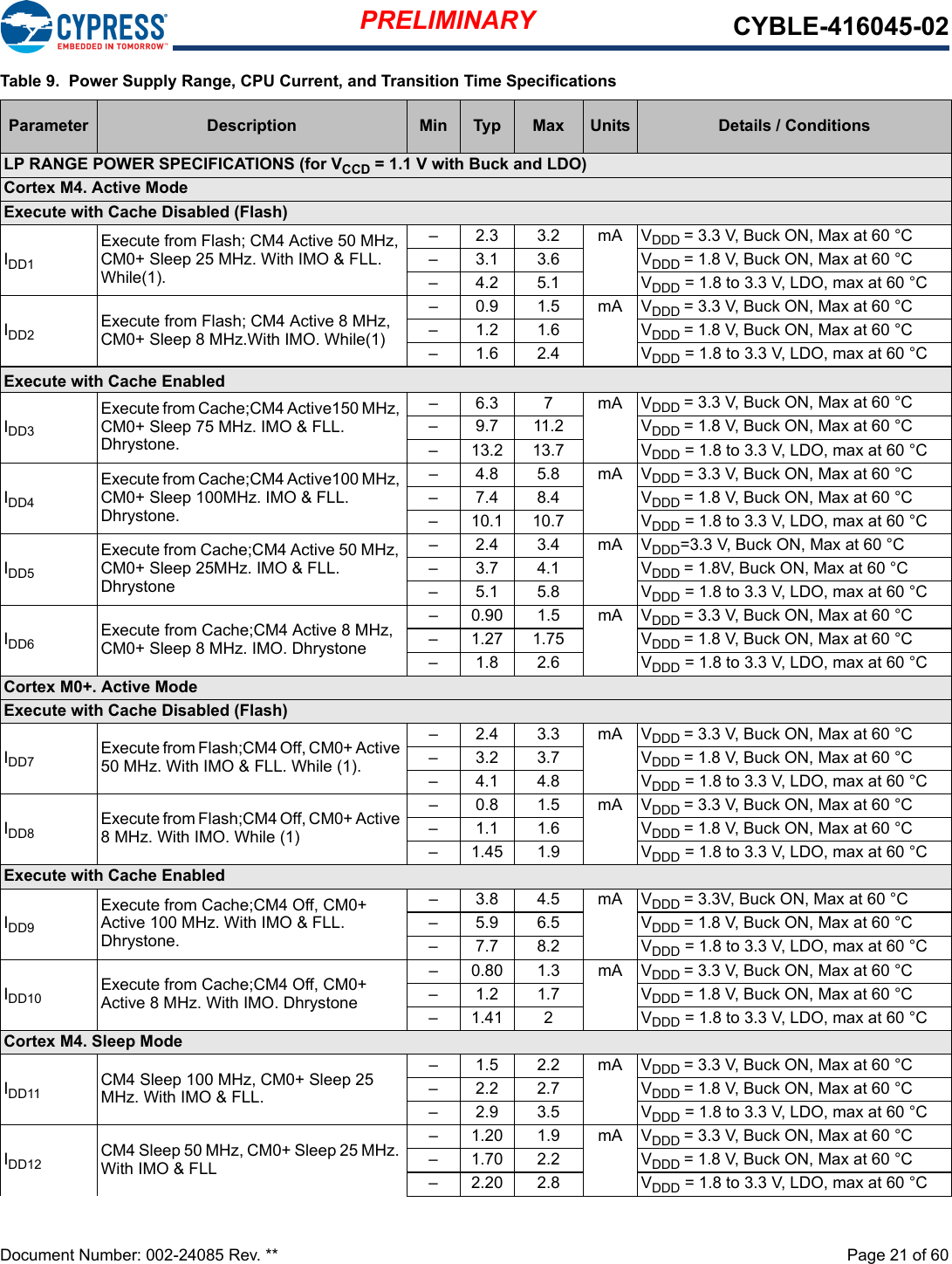
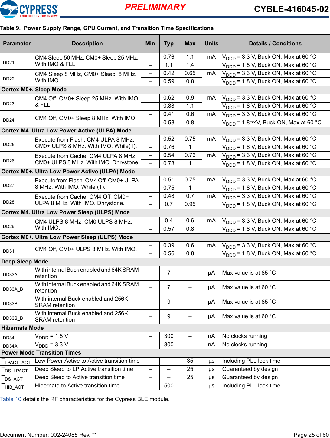
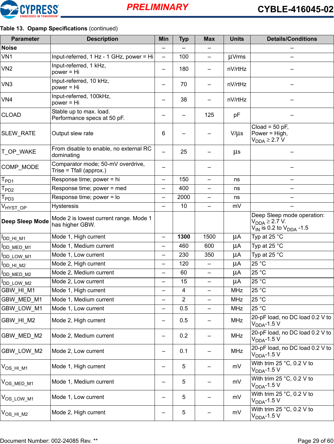
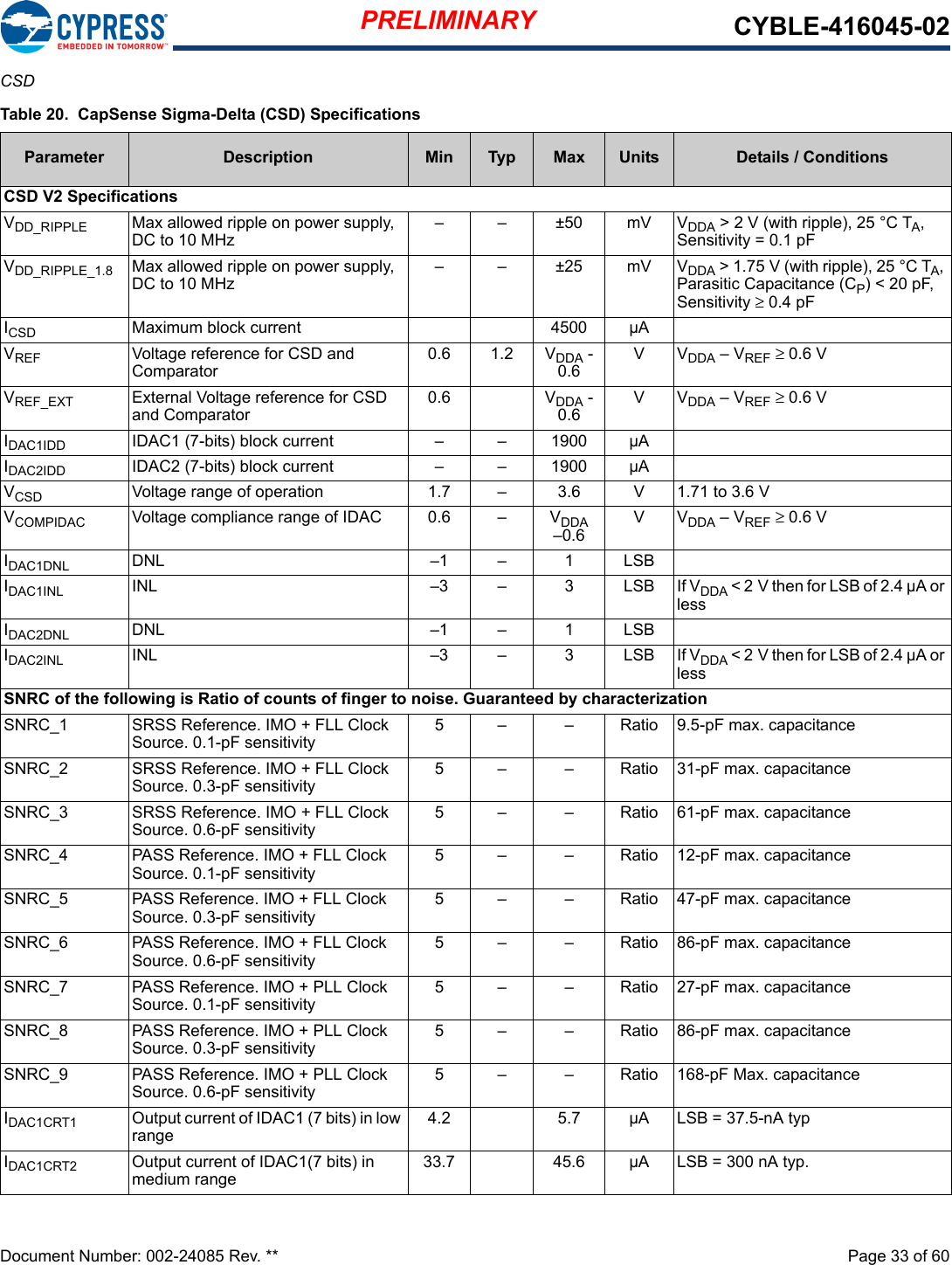
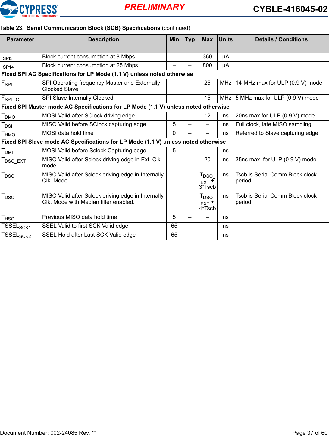
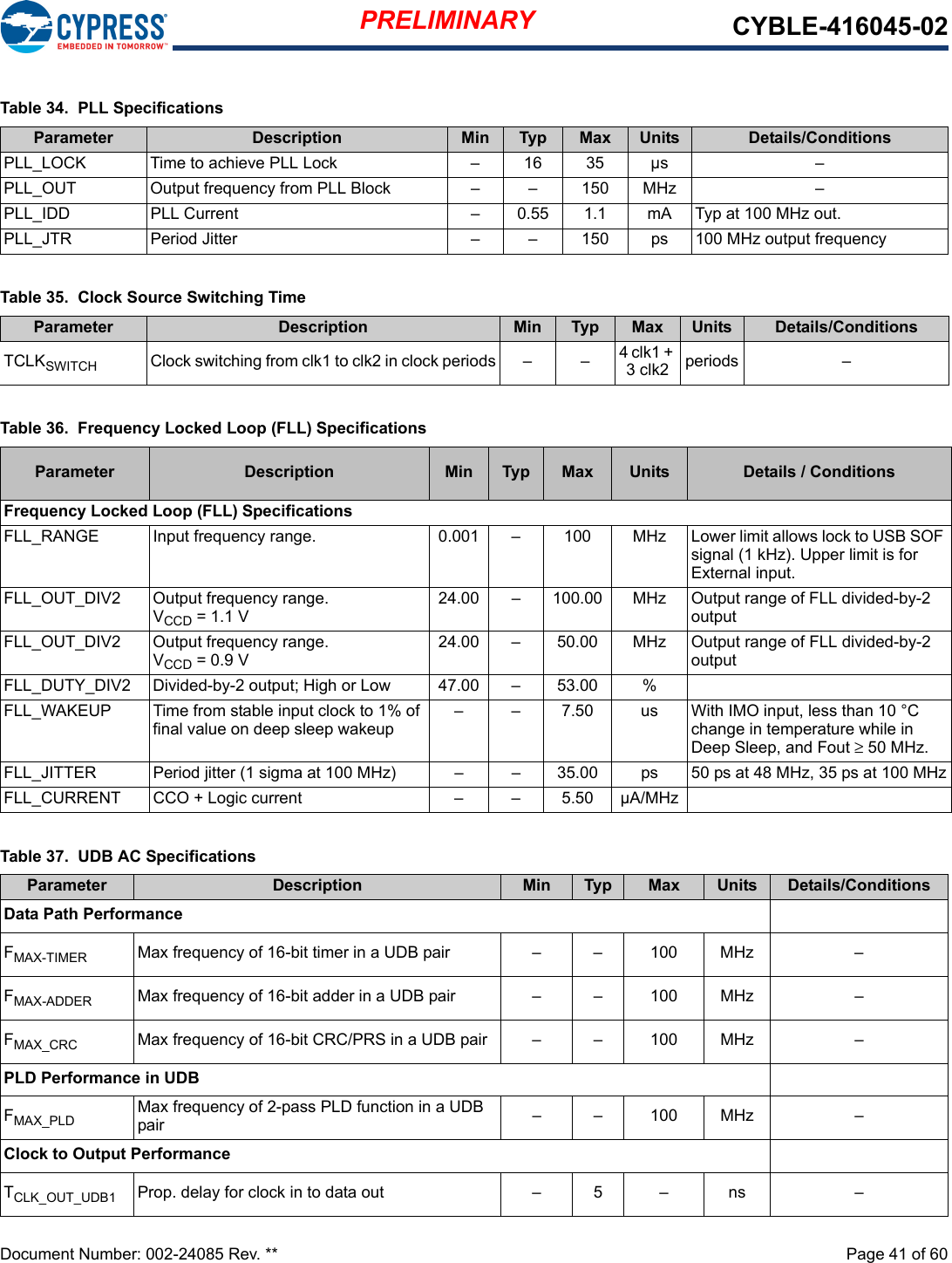
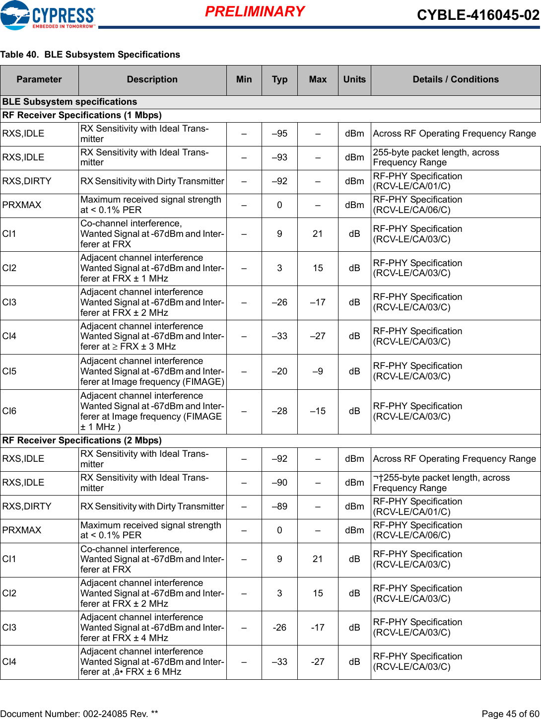
![PRELIMINARY CYBLE-416045-02Document Number: 002-24085 Rev. ** Page 20 of 60Electrical SpecificationTable 8 details the absolute maximum electrical characteristics for the Cypress BLE module.Table 8. CYBLE-416045-02 Absolute Maximum Ratings[5]Device-Level SpecificationsAll specifications are valid for –40 °C ≤ TA ≤ 85 °C and for 1.71 V to 3.6 V except where noted.Parameter Description Min Typ Max Unit Details/ConditionsVDDD_ABS VDD, VDDA and VDDR supply relative to VSS (VSSD = VSSA)–0.5 – 4 V Absolute maximumVCCD_ABS Direct digital core voltage input relative to VSSD –0.5 – 1.2 V Absolute maximumVDDD_RIPPLE Maximum power supply ripple for VDD, VDDA and VDDR input voltage – – 100 mV3.0V supplyRipple frequency of 100 kHz to 750 kHzVGPIO_ABS GPIO voltage –0.5 – VDD +0.5 V Absolute maximumIGPIO_ABS Maximum current per GPIO –25 – 25 mA Absolute maximumIGPIO_injection GPIO injection current per pin –0.5 – 0.5 mA Absolute maximum current injected per pinLU Pin current for latch up –100 100 mA Absolute maximumTable 9. Power Supply Range, CPU Current, and Transition Time SpecificationsParameter Description Min Typ Max Units Details / ConditionsDC SpecificationsVDDD Internal regulator and Port 1 GPIO supply 1.7 – 3.6 VVDDA Analog power supply voltage. Shorted to VDDIOA on PCB. 1.7 – 3.6 V Internally unregulated SupplyVDDIO1 GPIO Supply for Ports 5 to 8 when present 1.7 – 3.6 V VDDIO_1 must be ≥ to VDDA.VDDIO0 GPIO Supply for Ports 11 to 13 when present 1.7 – 3.6 VVDDIO0 Supply for E-Fuse Programming 2.38 2.5 2.62 V E-Fuse Programming VoltageVDDIOR GPIO supply for Ports 2 to 4 on BGA 124 only 1.7 – 3.6 VVDDIOA GPIO Supply for Ports 9 to 10. Shorted to VDDA on PCB. 1.7 – 3.6 VVDDUSB Supply for Port 14 (USB or GPIO) when present 1.7 – 3.6 V Min supply is 2.85 V for USBVBACKUP Backup Power and GPIO Port 0 supply when present 1.7 – 3.6 V Min. is 1.4 V in Backup modeVCCD1 Output voltage (for core logic bypass) – 1.1 – V High-speed modeVCCD2 Output voltage (for core logic bypass) – 0.9 – ULP mode. Valid for –20 to 85 °CCEFC External regulator voltage (VCCD) bypass 3.8 4.7 5.6 µF X5R ceramic or betterCEXC Power supply decoupling capacitor – 10 – µF X5R ceramic or betterNote5. Usage above the absolute maximum conditions listed in Table 8 may cause permanent damage to the device. Exposure to absolute maximum conditions for extended periods of time may affect device reliability. The maximum storage temperature is 150 °C in compliance with JEDEC Standard JESD22-A103, High Temperature Storage Life. When used below absolute maximum conditions but above normal operating conditions, the device may not operate to specification.](https://usermanual.wiki/Cypress-Semiconductor/6045/User-Guide-3880583-Page-20.png)
![PRELIMINARY CYBLE-416045-02Document Number: 002-24085 Rev. ** Page 49 of 60Environmental SpecificationsEnvironmental ComplianceThis Cypress BLE module is built in compliance with the Restriction of Hazardous Substances (RoHS) and Halogen Free (HF)directives. The Cypress module and components used to produce this module are RoHS and HF compliant.RF CertificationThe CYBLE-416045-02 module is certified under the following RF certification standards:n FCC ID: WAP6045n CEn IC: 7922A-6045n MIC: TBDEnvironmental ConditionsTable 42 describes the operating and storage conditions for the Cypress BLE module.Table 42. Environmental Conditions for CYBLE-416045-02ESD and EMI ProtectionExposed components require special attention to ESD and electromagnetic interference (EMI).A grounded conductive layer inside the device enclosure is suggested for EMI and ESD performance. Any openings in the enclosure near the module should be surrounded by a grounded conductive layer to provide ESD protection and a low-impedance path to ground. Device Handling: Proper ESD protocol must be followed in manufacturing to ensure component reliability.Description Minimum Specification Maximum Specification85 °C–40 °COperating temperature85%5%Operating humidity (relative, non-condensation)Thermal ramp rate 3 °C/minute–Storage temperature 85 °C–40 °CStorage temperature and humidity 85 ° C at 85%–ESD: Module integrated into system Components[9] –15 kV Air2.2 kV ContactNote9. This does not apply to the RF pins (ANT, XTALI, and XTALO). RF pins (ANT, XTALI, and XTALO) are tested for 500-V HBM.](https://usermanual.wiki/Cypress-Semiconductor/6045/User-Guide-3880583-Page-49.png)