Cypress Semiconductor 4110 Bluetooth Module User Manual CYBLE 224110 00 EZ BLE TM PSoC XT XR Module
Cypress Semiconductor Bluetooth Module CYBLE 224110 00 EZ BLE TM PSoC XT XR Module
UserManual.wiki
>
Cypress Semiconductor
>
4110 User Manual
>
User Manual
Contents
1.
User Manual
2.
User Manual II
User Manual
Navigation menu
Upload a User Manual
Namespaces
Wiki Guide
HTML
PDF
Info
Views
User Manual
Discussion / Help
Navigation
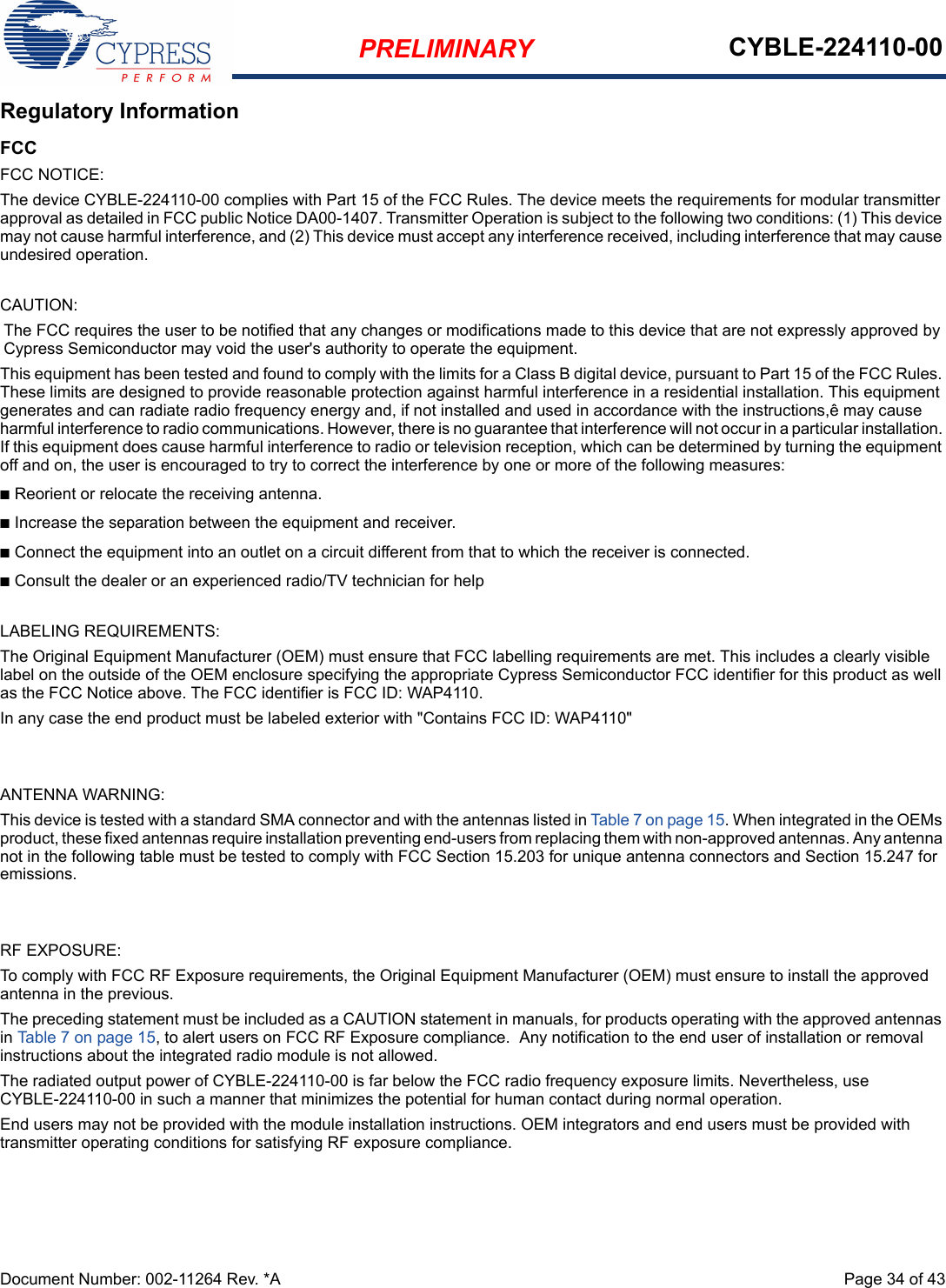
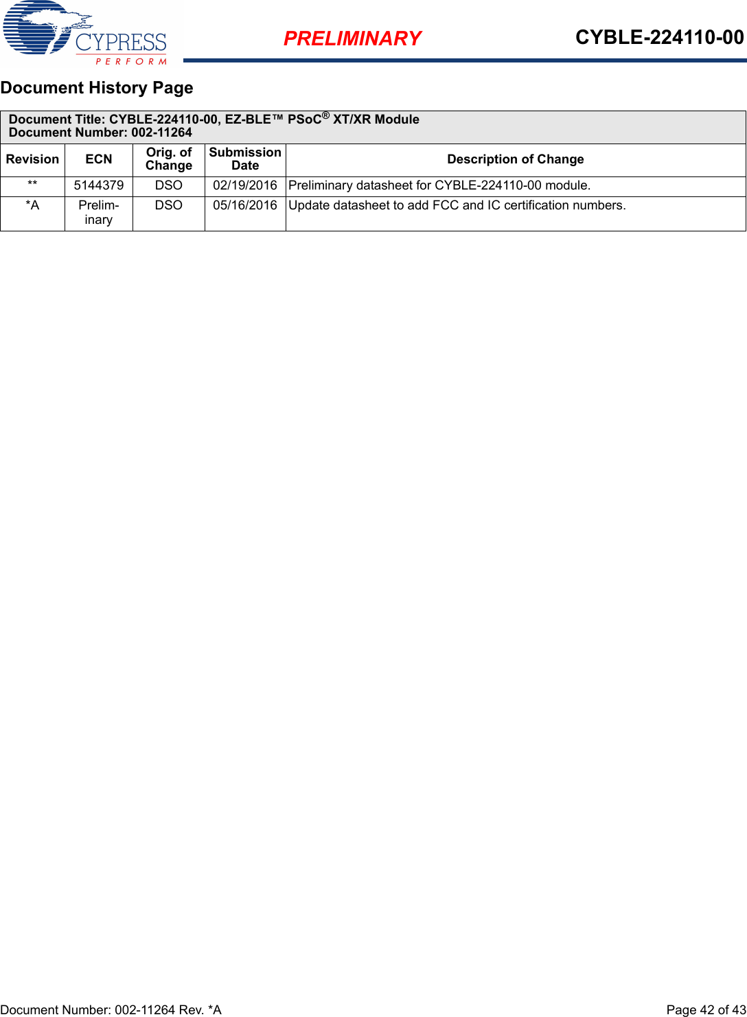
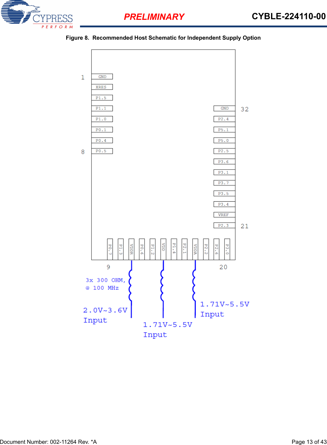
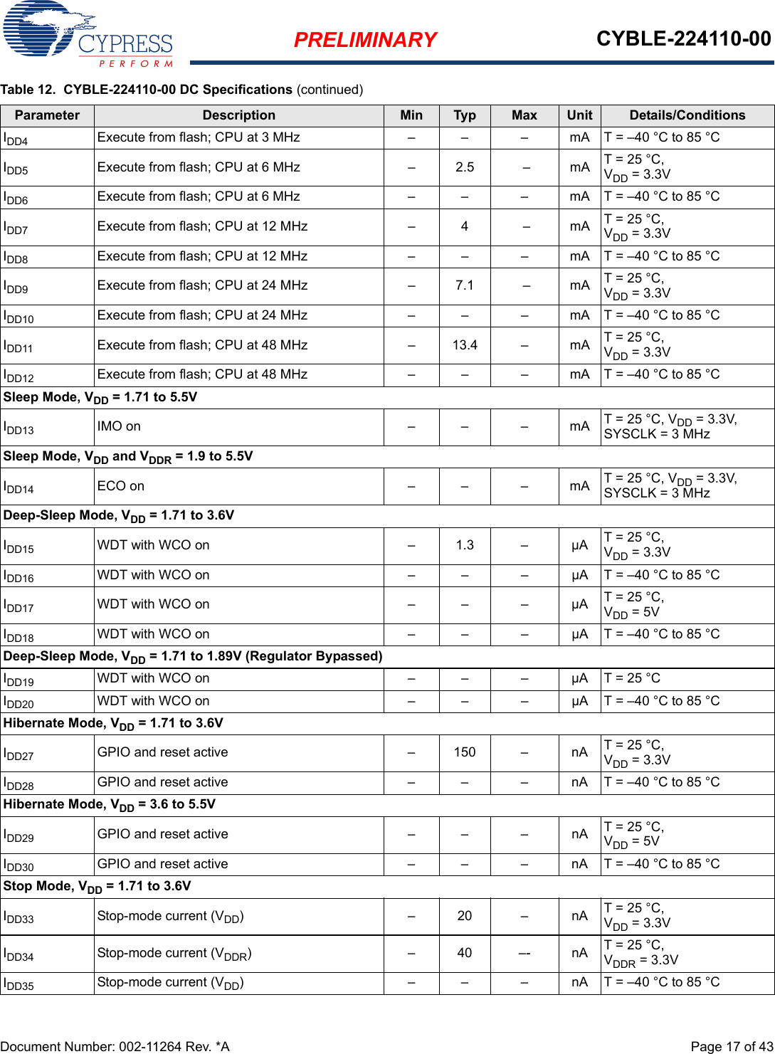
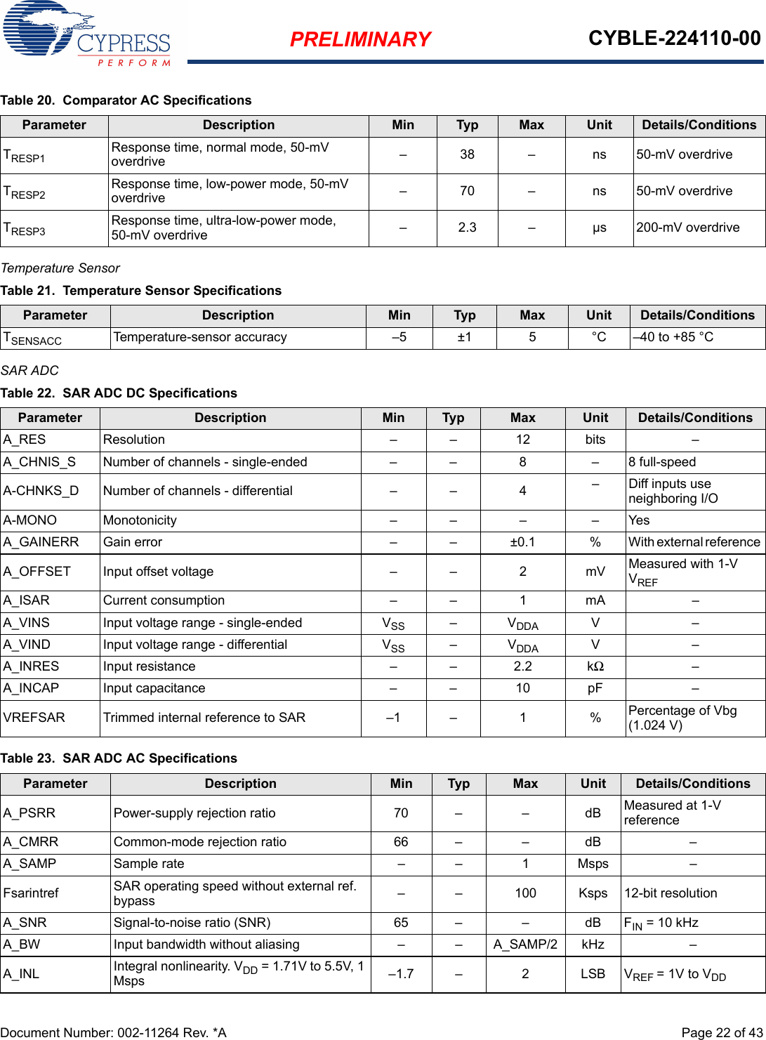
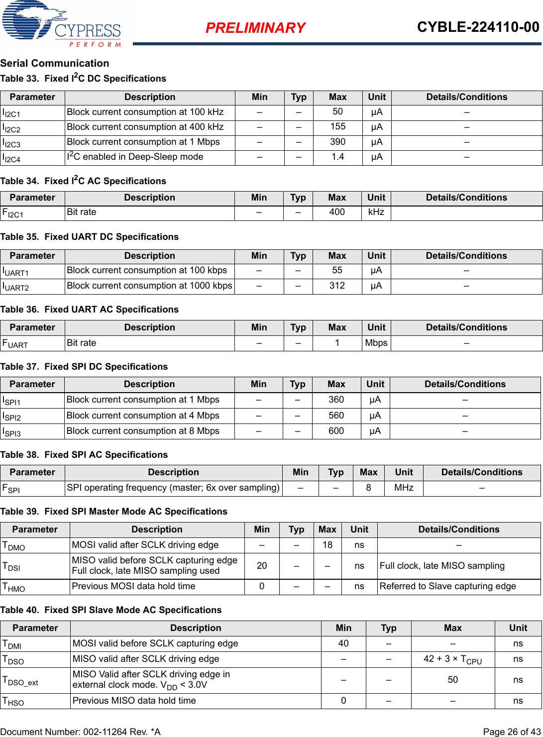
![PRELIMINARY CYBLE-224110-00Document Number: 002-11264 Rev. *A Page 10 of 43Table 4 and Table 5 detail the solder pad connection definitions and available functions for each connection pad. Table 5 lists the solder pads on CYBLE-224110-00, the BLE device port-pin, and denotes whether the digital function shown is available for each solder pad. Table 5 denotes whether the analog function shown is available for each solder pad. Each connection is configurable for a single option shown with a 3.Table 4. Digital Peripheral CapabilitiesPad NumberDevice Port Pin UART SPI I2CTCPWM[2] CapSenseWCO OutECO OUT LCD SWD GPIO1GND[3] Ground Connection2 XRES External Reset Hardware Connection Input3P1.53(SCB0_TX) 3(SCB0_MISO) 3(SCB0_SCL) 3(TCPWM2_N) 3334P1.1 3(SCB1_SS1) 3(TCPWM0_N) 3335P1.0 3(TCPWM0_P) 3336P0.13(SCB1_TX) 3(SCB1_MISO) 3(SCB1_SCL) 3(TCPWM0_N) 3337P0.43(SCB0_RX) 3(SCB0_MOSI) 3(SCB0_SDA) 3(TCPWM1_P) 333 38P0.53(SCB0_TX) 3(SCB0_MISO) 3(SCB0_SCL) 3(TCPWM1_N) 3339P0.73(SCB0_CTS) 3(SCB0_SCLK) 3(TCPWM2_N) 333(SWDCLK) 310 P1.3 3(SCB1_SS3) 3(TCPWM1_N) 33311 VDDR Radio Power Supply (2.0V to 3.6V)12 P0.6 3(SCB0_RTS) 3(SCB0_SS0) 3(TCPWM2_P) 333(SWDIO) 313 P1.2 3(SCB1_SS2) 3(TCPWM1_P) 33314 VDD Digital Power Supply Input (1.71 to 5.5V)15 P1.4 3(SCB0_RX) 3(SCB0_MOSI) 3(SCB0_SDA) 3(TCPWM2_P) 33316 P2.1 3(SCB0_SS2) 33317 VDDA Analog Power Supply Input (1.71 to 5.5V)18 P2.2 3(SCB0_SS3) 33319 P2.6 33320 P3.0 3(SCB0_RX) 3(SCB0_SDA) 3(TCPWM0_P) 33321 P2.3 33 3 322 VREF Reference Voltage Input23 P3.4 3(SCB1_RX) 3(SCB1_SDA) 3(TCPWM2_P) 33324 P3.5 3(SCB1_TX) 3(SCB1_SCL) 3(TCPWM2_N) 33325 P3.7 3(SCB1_CTS) 3(TCPWM3_N) 33 3 326 P3.1 3(SCB0_TX) 3(SCB0_SCL) 3(TCPWM0_N) 33327 P3.6 3(SCB1_RTS) 3(TCPWM3_P) 33328 P2.5 33329 P5.0 3(SCB1_RX) 3(SCB1_SS0) 3(SCB1_SDA) 3(TCPWM3_P) 33330 P5.1 3(SCB1_TX) 3(SCB1_SCLK) 3(SCB1_SCL) 3(TCPWM3_N) 333 331 P2.4 33332 GND[3] Ground Connection](https://usermanual.wiki/Cypress-Semiconductor/4110.User-Manual/User-Guide-3001048-Page-10.png)
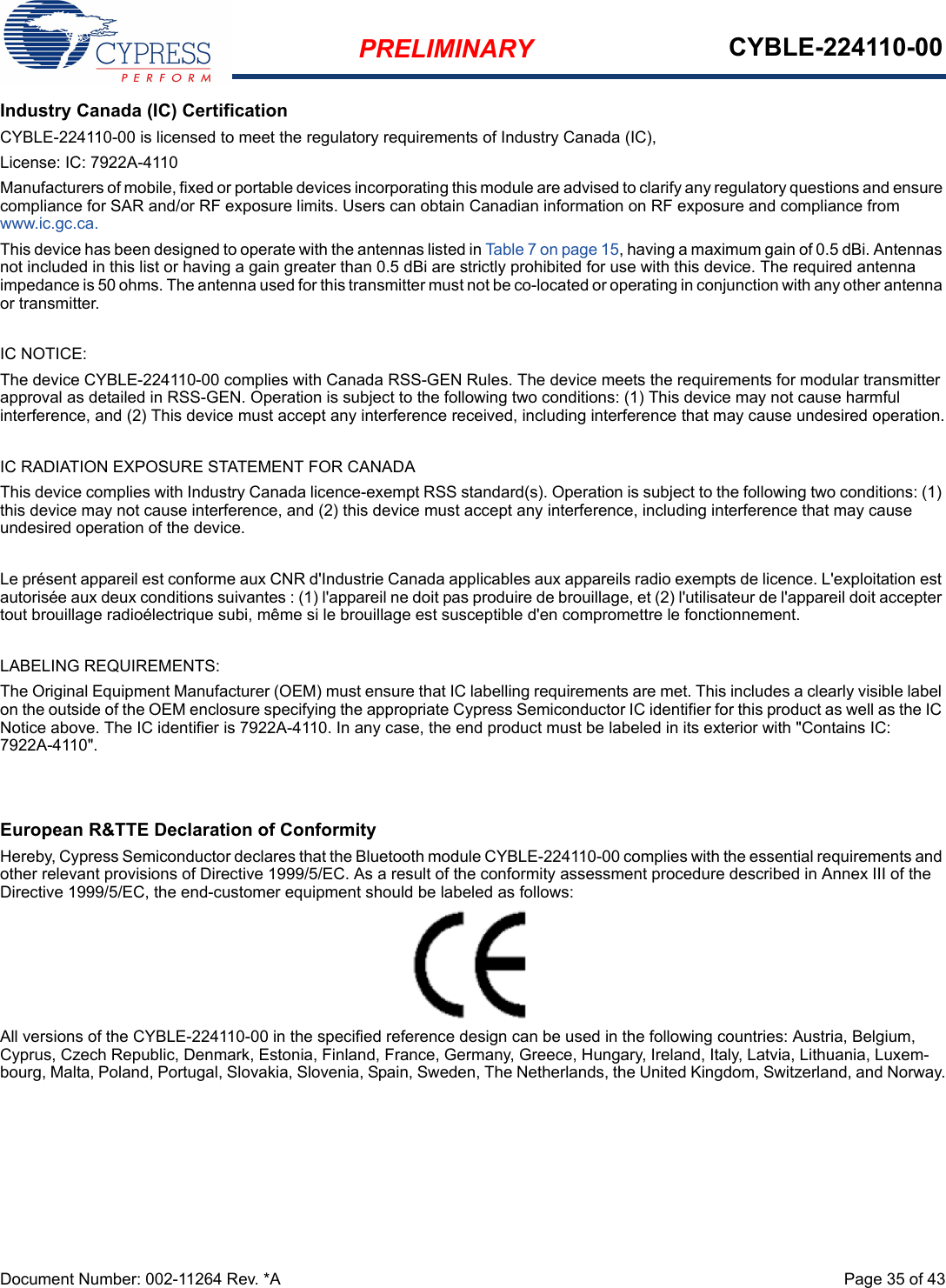
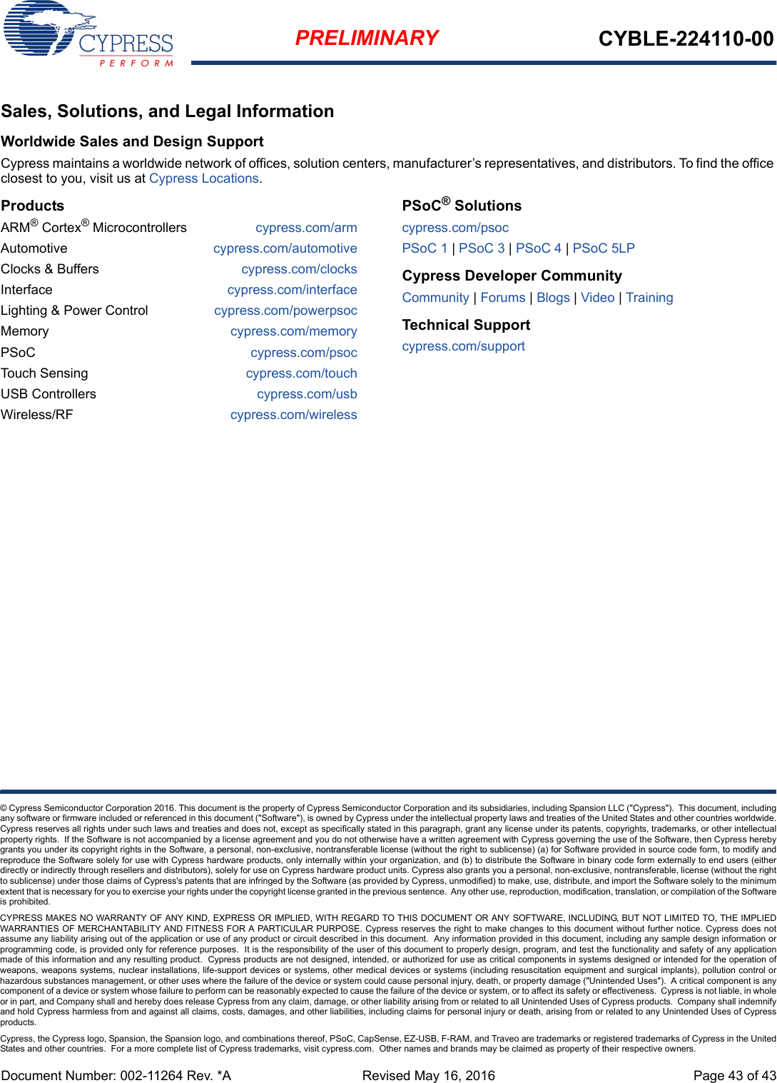
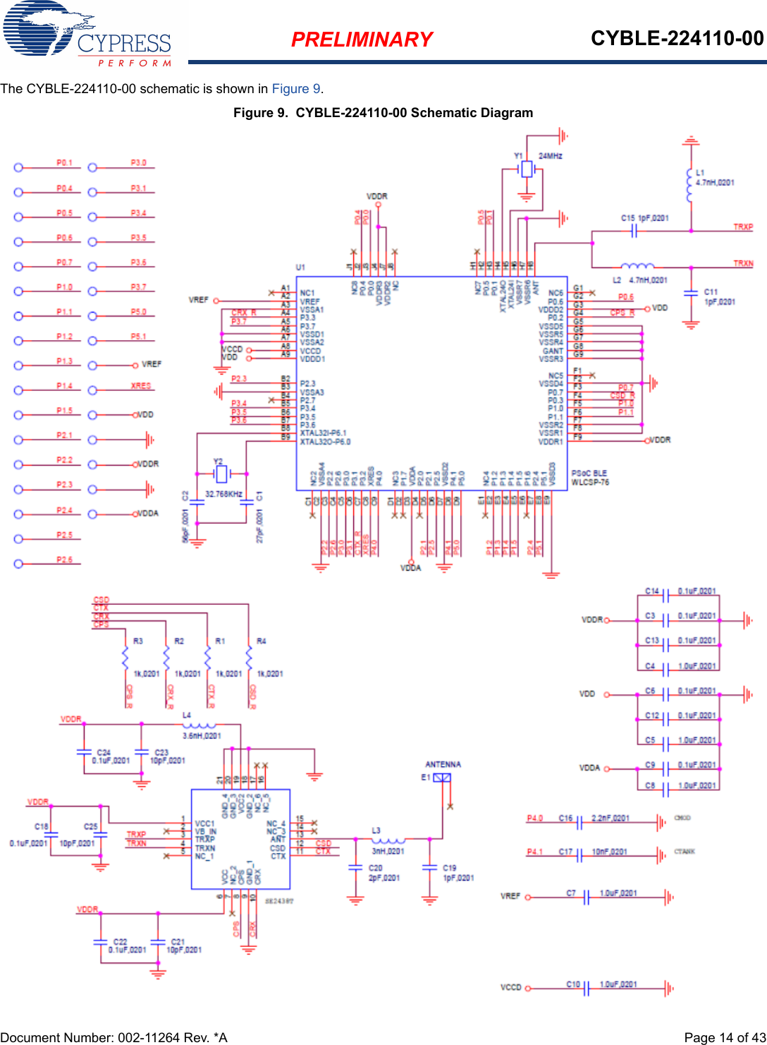
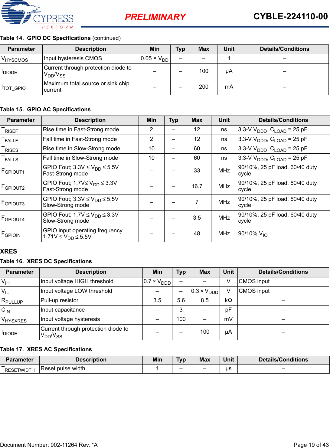
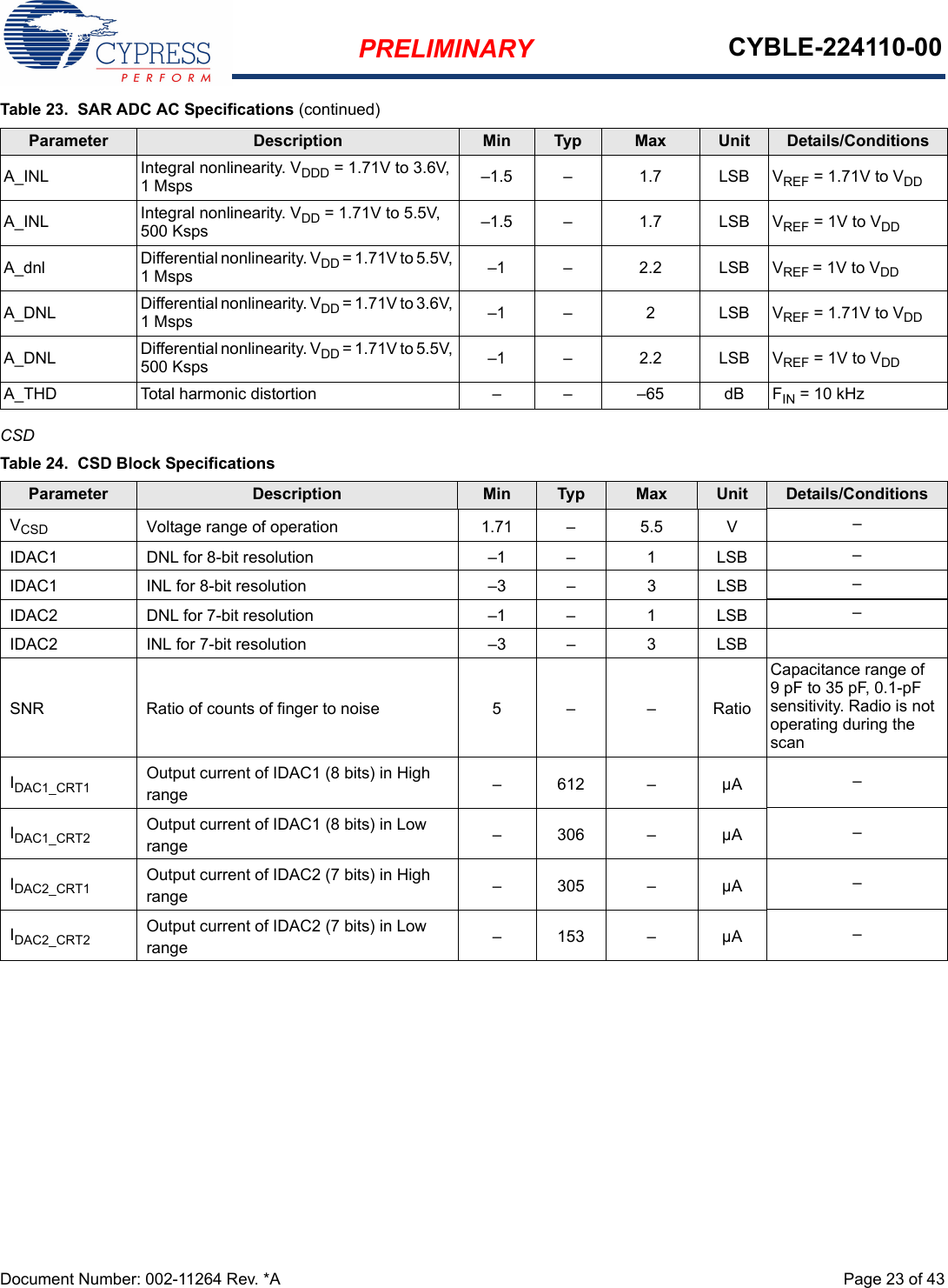
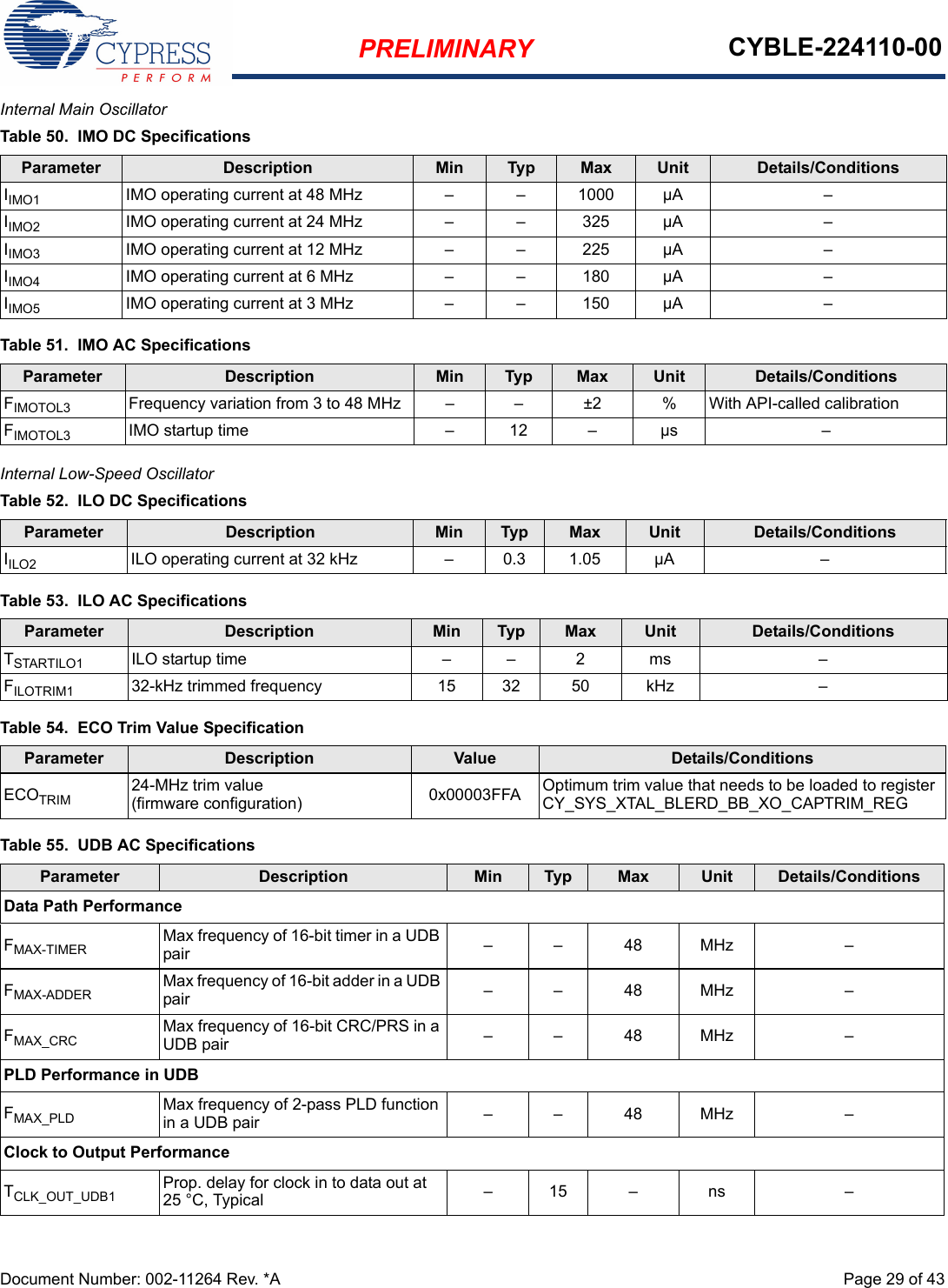
![PRELIMINARY CYBLE-224110-00Document Number: 002-11264 Rev. *A Page 11 of 43Notes2. TCPWM stands for timer, counter, and PWM. If supported, the pad can be configured to any of these peripheral functions.3. The main board needs to connect both GND connections (Pad 1 and Pad 32) on the module to the common ground of the system. Table 5. Analog Peripheral CapabilitiesPad Number Device Port Pin SARMUX OPAMP LPCOMP1GND[3] Ground Connection2 XRES External Reset Hardware Connection Input3P1.5 −3(CTBm1_OA1_INP) −4P1.1 −3(CTBm1_OA0_INN) −5P1.0 −3(CTBm1_OA0_INP) −6P0.1 −−3(COMP0_INN)7P0.4 −−3(COMP1_INP)8P0.5 −−3(COMP1_INN)9P0.7 −− −10 P1.3 −3(CTBm1_OA1_OUT) −11 VDDR Radio Power Supply (2.0V to 3.6V)12 P0.6 −− −13 P1.2 −3(CTBm1_OA0_OUT) −14 VDD Digital Power Supply Input (1.71 to 5.5V)15 P1.4 −3(CTBm1_OA1_INN) −16 P2.1 −3(CTBm1_OA0_INN) −17 VDDA Analog Power Supply Input (1.71 to 5.5V)18 P2.2 −3(CTBm1_OA0_OUT) −19 P2.6 −3(CTBm1_OA0_INP) −20 P3.0 3−−21 P2.3 −3(CTBm1_OA1_OUT) −22 VREF Reference Voltage Input (Optional)23 P3.4 3−−24 P3.5 3−−25 P3.7 3−−26 P3.1 3−−27 P3.6 3−−28 P2.5 −3(CTBm0_OA1_INP) −29 P5.0 −− −30 P5.1 −− −31 P2.4 −3(CTBm0_OA1_INN) −32 GND Ground Connection](https://usermanual.wiki/Cypress-Semiconductor/4110.User-Manual/User-Guide-3001048-Page-11.png)
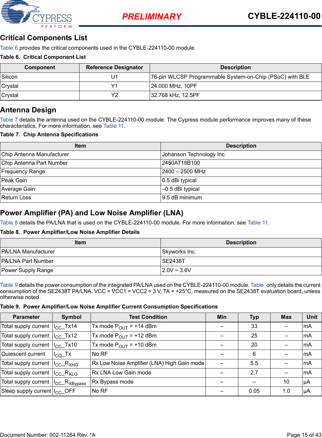
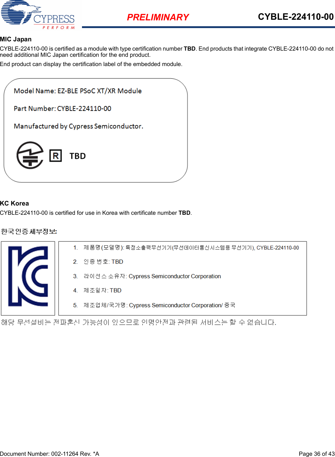
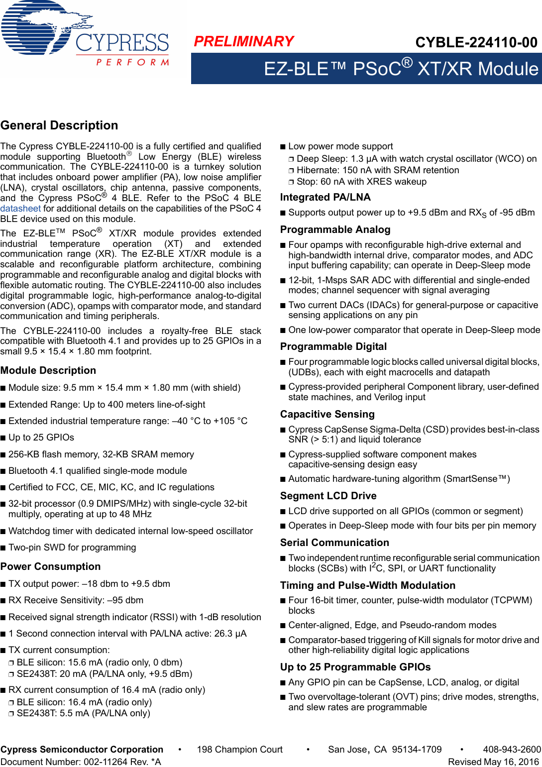
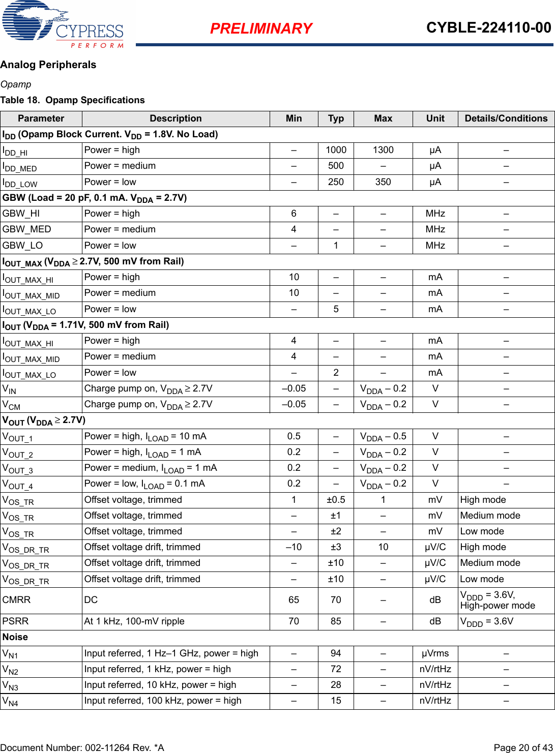
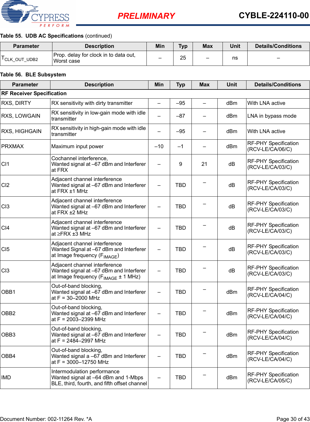
![PRELIMINARY CYBLE-224110-00Document Number: 002-11264 Rev. *A Page 18 of 43GPIOIDD36 Stop-mode current (VDDR)–––nAT = –40 °C to 85 °C, VDDR = 1.9V to 3.6VStop Mode, VDD = 3.6 to 5.5VIDD37 Stop-mode current (VDD)–––nAT = 25 °C, VDD = 5VIDD38 Stop-mode current (VDDR)–––nAT = 25 °C, VDDR = 5VIDD39 Stop-mode current (VDD) – – – nA T = –40 °C to 85 °CIDD40 Stop-mode current (VDDR) – – – nA T = –40 °C to 85 °CTable 12. CYBLE-224110-00 DC Specifications (continued)Parameter Description Min Typ Max Unit Details/ConditionsNote4. VIH must not exceed VDD + 0.2V.Table 13. AC SpecificationsParameter Description Min Typ Max Unit Details/ConditionsFCPU CPU frequency DC – 48 MHz 1.71V ≤ VDD ≤ 5.5VTSLEEP Wakeup from Sleep mode – 0 – µs Guaranteed by characterizationTDEEPSLEEP Wakeup from Deep-Sleep mode – – 25 µs 24-MHz IMO. Guaranteed by characterizationTHIBERNATE Wakeup from Hibernate mode – – 800 µs Guaranteed by characterizationTSTOP Wakeup from Stop mode – – 2 ms XRES wakeupTable 14. GPIO DC SpecificationsParameter Description Min Typ Max Unit Details/ConditionsVIH[4]Input voltage HIGH threshold 0.7 × VDD – – V CMOS inputLVTTL input, VDD < 2.7V 0.7 × VDD – – V –LVTTL input, VDD ≥ 2.7V 2.0 – – V –VILInput voltage LOW threshold – – 0.3 × VDD VCMOS inputLVTTL input, VDD < 2.7V – – 0.3 × VDD V–LVTTL input, VDD ≥ 2.7V – – 0.8 V –VOHOutput voltage HIGH level VDD –0.6 – – V IOH = 4 mA at 3.3-V VDD Output voltage HIGH level VDD –0.5 – – V IOH = 1 mA at 1.8-V VDDVOLOutput voltage LOW level – – 0.6 V IOL = 8 mA at 3.3-V VDDOutput voltage LOW level – – 0.6 V IOL = 4 mA at 1.8-V VDDOutput voltage LOW level – – 0.4 V IOL = 3 mA at 3.3-V VDDRPULLUP Pull-up resistor 3.5 5.6 8.5 kΩ–RPULLDOWN Pull-down resistor 3.5 5.6 8.5 kΩ–IIL Input leakage current (absolute value) – – 2 nA 25 °C, VDD = 3.3 VIIL_CTBM Input leakage on CTBm input pins – – 4 nA –CIN Input capacitance – – 7 pF –VHYSTTL Input hysteresis LVTTL 25 40 – mV VDD > 2.7 V](https://usermanual.wiki/Cypress-Semiconductor/4110.User-Manual/User-Guide-3001048-Page-18.png)
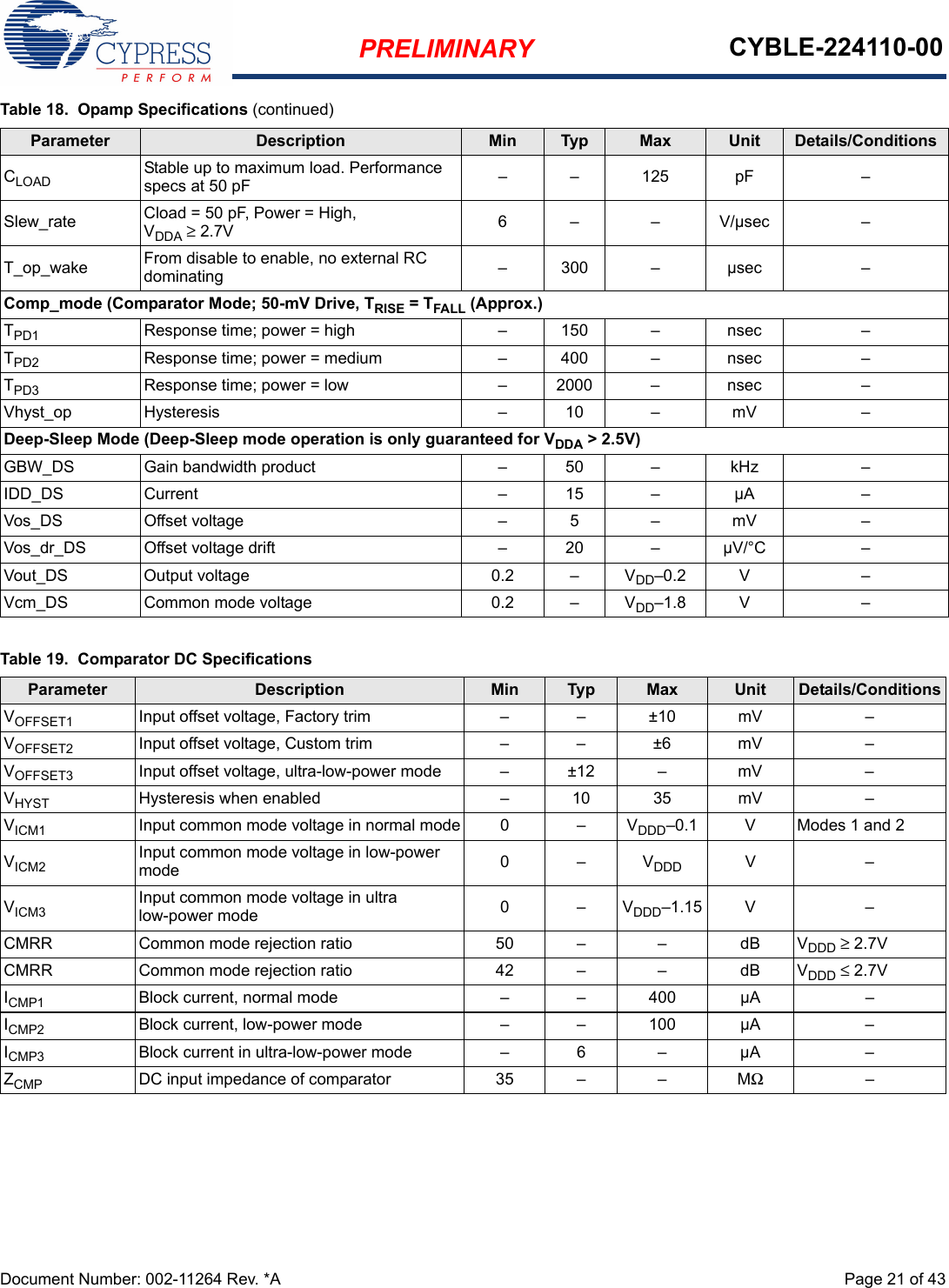
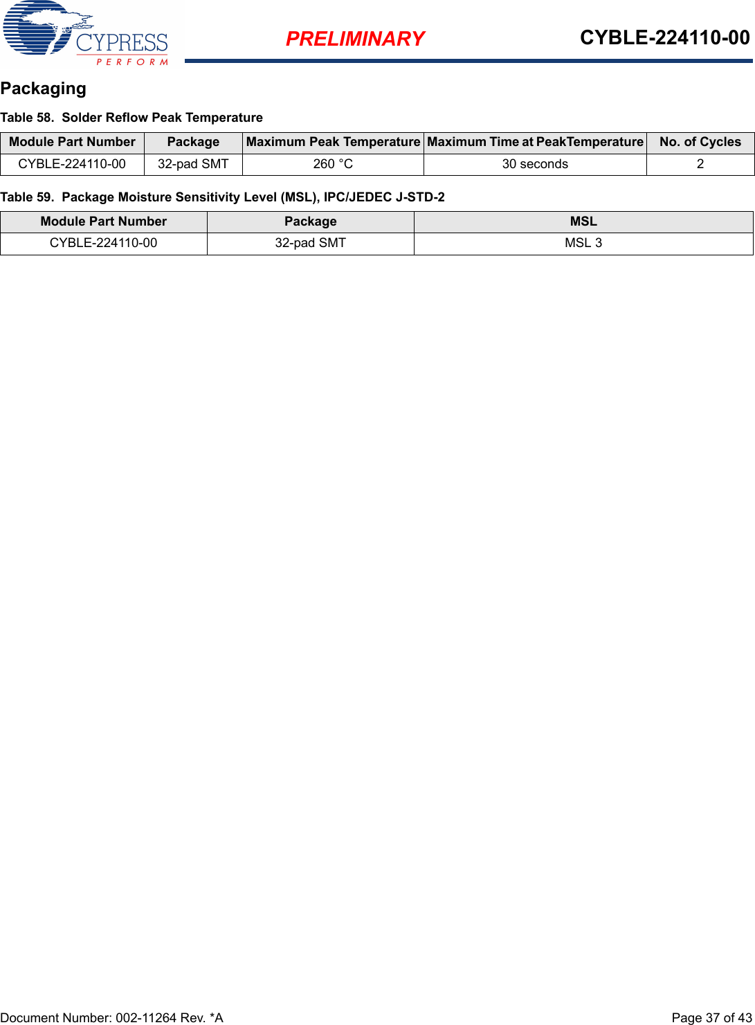
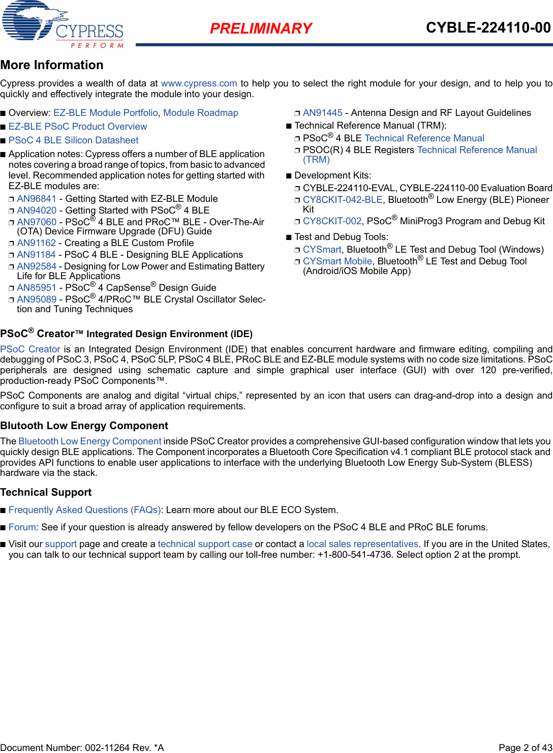
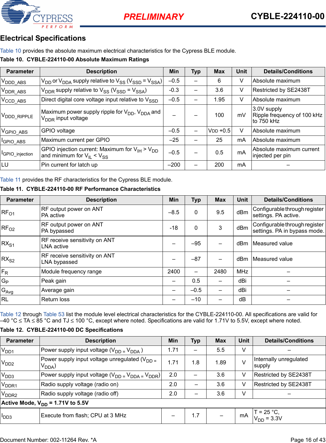
![PRELIMINARY CYBLE-224110-00Document Number: 002-11264 Rev. *A Page 27 of 43MemorySystem ResourcesPower-on-Reset (POR) TSSELSCK SSEL valid to first SCK valid edge 100 – – nsTable 40. Fixed SPI Slave Mode AC Specifications (continued)Parameter Description Min Typ Max UnitNote5. It can take as much as 20 ms to write to flash. During this time, the device should not be reset, or flash operations will be interrupted and cannot be relied on to have completed. Reset sources include the XRES pin, software resets, CPU lockup states and privilege violations, improper power supply levels, and watchdogs. Make certain that these are not inadvertently activated.Table 41. Flash DC SpecificationsParameter Description Min Typ Max Unit Details/ConditionsVPE Erase and program voltage 1.71 – 5.5 V –TWS48 Number of Wait states at 32–48 MHz 2 – – – CPU execution from flashTWS32 Number of Wait states at 16–32 MHz 1 – – – CPU execution from flashTWS16 Number of Wait states for 0–16 MHz 0 – – – CPU execution from flashTable 42. Flash AC SpecificationsParameter Description Min Typ Max Unit Details/ConditionsTROWWRITE[5] Row (block) write time (erase and program) – – 20 ms Row (block) = 256 bytesTROWERASE[5] Row erase time – – 13 ms –TROWPROGRAM[5] Row program time after erase – – 7 ms –TBULKERASE[5] Bulk erase time (256 KB) – – 35 ms –TDEVPROG[5] Total device program time – – 25 seconds –FEND Flash endurance 100 K – – cycles –FRET Flash retention. TA ≤ 55 °C, 100 K P/E cycles 20 – – years –FRET2 Flash retention. TA ≤ 85 °C, 10 K P/E cycles 10 – – years –Table 43. POR DC SpecificationsParameter Description Min Typ Max Unit Details/ConditionsVRISEIPOR Rising trip voltage 0.80 – 1.45 V –VFALLIPOR Falling trip voltage 0.75 – 1.40 V –VIPORHYST Hysteresis 15 – 200 mV –Table 44. POR AC SpecificationsParameter Description Min Typ Max Unit Details/ConditionsTPPOR_TR Precision power-on reset (PPOR) response time in Active and Sleep modes ––1µs –Table 45. Brown-Out DetectParameter Description Min Typ Max Unit Details/ConditionsVFALLPPOR BOD trip voltage in Active and Sleep modes 1.64 – – V –VFALLDPSLP BOD trip voltage in Deep Sleep 1.4 – – V –](https://usermanual.wiki/Cypress-Semiconductor/4110.User-Manual/User-Guide-3001048-Page-27.png)
![PRELIMINARY CYBLE-224110-00Document Number: 002-11264 Rev. *A Page 28 of 43Voltage Monitors (LVD) SWD Interface Table 46. Hibernate ResetParameter Description Min Typ Max Unit Details/ConditionsVHBRTRIP BOD trip voltage in Hibernate 1.1 – – V –Table 47. Voltage Monitor DC SpecificationsParameter Description Min Typ Max Unit Details/ConditionsVLVI1 LVI_A/D_SEL[3:0] = 0000b 1.71 1.75 1.79 V –VLVI2 LVI_A/D_SEL[3:0] = 0001b 1.76 1.80 1.85 V –VLVI3 LVI_A/D_SEL[3:0] = 0010b 1.85 1.90 1.95 V –VLVI4 LVI_A/D_SEL[3:0] = 0011b 1.95 2.00 2.05 V –VLVI5 LVI_A/D_SEL[3:0] = 0100b 2.05 2.10 2.15 V –VLVI6 LVI_A/D_SEL[3:0] = 0101b 2.15 2.20 2.26 V –VLVI7 LVI_A/D_SEL[3:0] = 0110b 2.24 2.30 2.36 V –VLVI8 LVI_A/D_SEL[3:0] = 0111b 2.34 2.40 2.46 V –VLVI9 LVI_A/D_SEL[3:0] = 1000b 2.44 2.50 2.56 V –VLVI10 LVI_A/D_SEL[3:0] = 1001b 2.54 2.60 2.67 V –VLVI11 LVI_A/D_SEL[3:0] = 1010b 2.63 2.70 2.77 V –VLVI12 LVI_A/D_SEL[3:0] = 1011b 2.73 2.80 2.87 V –VLVI13 LVI_A/D_SEL[3:0] = 1100b 2.83 2.90 2.97 V –VLVI14 LVI_A/D_SEL[3:0] = 1101b 2.93 3.00 3.08 V –VLVI15 LVI_A/D_SEL[3:0] = 1110b 3.12 3.20 3.28 V –VLVI16 LVI_A/D_SEL[3:0] = 1111b 4.39 4.50 4.61 V –LVI_IDD Block current – – 100 µA –Table 48. Voltage Monitor AC SpecificationsParameter Description Min Typ Max Unit Details/ConditionsTMONTRIP Voltage monitor trip time – – 1 µs –Table 49. SWD Interface SpecificationsParameter Description Min Typ Max Unit Details/ConditionsF_SWDCLK1 3.3V ≤ VDD ≤ 5.5V – – 14 MHz SWDCLK ≤ 1/3 CPU clock frequencyF_SWDCLK2 1.71V ≤ VDD ≤ 3.3V – – 7 MHz SWDCLK ≤ 1/3 CPU clock frequencyT_SWDI_SETUP T = 1/f SWDCLK 0.25 × T – – ns –T_SWDI_HOLD T = 1/f SWDCLK 0.25 × T – – ns –T_SWDO_VALID T = 1/f SWDCLK – – 0.5 × T ns –T_SWDO_HOLD T = 1/f SWDCLK 1 – – ns –](https://usermanual.wiki/Cypress-Semiconductor/4110.User-Manual/User-Guide-3001048-Page-28.png)
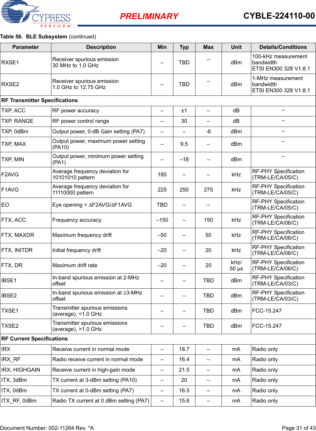
![PRELIMINARY CYBLE-224110-00Document Number: 002-11264 Rev. *A Page 33 of 43Environmental SpecificationsEnvironmental ComplianceThis Cypress BLE module is built in compliance with the Restriction of Hazardous Substances (RoHS) and Halogen Free (HF) directives. The Cypress module and components used to produce this module are RoHS and HF compliant.RF CertificationThe CYBLE-224110-00 module is certified under the following RF certification standards:nFCC ID: WAP4110nCEnIC: 7922A-4110nMICnKCEnvironmental ConditionsTable 57 describes the operating and storage conditions for the Cypress BLE module.ESD and EMI ProtectionExposed components require special attention to ESD and electromagnetic interference (EMI).A grounded conductive layer inside the device enclosure is suggested for EMI and ESD performance. Any openings in the enclosure near the module should be surrounded by a grounded conductive layer to provide ESD protection and a low-impedance path to ground. Device Handling: Proper ESD protocol must be followed in manufacturing to ensure component reliability.Table 57. Environmental Conditions for CYBLE-224110-00Description Minimum Specification Maximum SpecificationOperating temperature –40 °C 105 °COperating humidity (relative, non-condensation) 5% 85%Thermal ramp rate – 3 °C/minuteStorage temperature –40 °C 105 °CStorage temperature and humidity – 105 ° C at 85%ESD: Module integrated into system Components[6] –15 kV Air2.2 kV ContactNote6. This does not apply to the RF pins (ANT, XTALI, and XTALO). RF pins (ANT, XTALI, and XTALO) are tested for 500-V HBM.](https://usermanual.wiki/Cypress-Semiconductor/4110.User-Manual/User-Guide-3001048-Page-33.png)