Cypress Semiconductor 3136 Bluetooth wireless EZ-BLE Module with HomeKit User Manual CYBT 013033 01 EZ BT Module
Cypress Semiconductor Bluetooth wireless EZ-BLE Module with HomeKit CYBT 013033 01 EZ BT Module
UserManual.wiki
>
Cypress Semiconductor
>
3136 User Manual
>
User Manual
Contents
1.
User Manual
2.
Use rmanual_CYBLE-473142-01
3.
Use rmanual_CYBLE-473148-01
4.
User Manual_CYBLE-413136-01
5.
User Manual_CYBLE-413149-01
6.
User manual_CYBLE-473142-01
7.
User manual_CYBLE-473148-01
User Manual
Navigation menu
Upload a User Manual
Namespaces
Wiki Guide
HTML
PDF
Info
Views
User Manual
Discussion / Help
Navigation
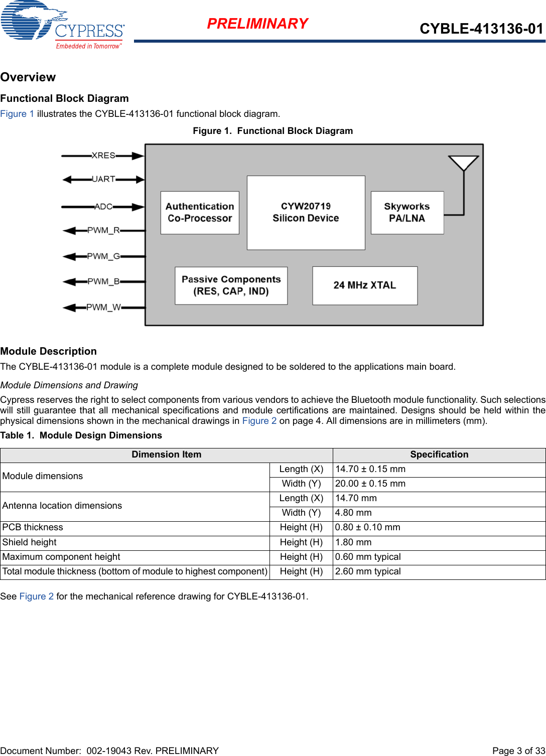
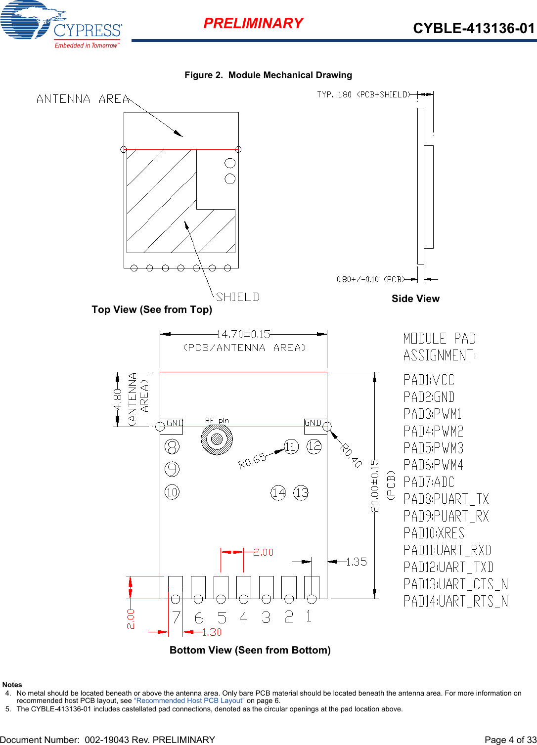
![PRELIMINARY CYBLE-413136-01EZ-BLE™ Module with HomeKitCypress Semiconductor Corporation • 198 Champion Court • San Jose,CA 95134-1709 • 408-943-2600Document Number: 002-19043 Rev. PRELIMINARY Revised May 12, 2017General DescriptionThe CYBLE-413136-01 is a Bluetooth Low Energy (BLE)wireless module solution with integrated Apple HomeKit support,including the authentication co-processor. TheCYBLE-413136-01 includes onboard crystal oscillators, passivecomponents, and the Cypress CYW20719 silicon device. The CYBLE-413136-01 supports a number of peripheralfunctions (ADC and PWM), as well as UART serialcommunication protocol. The CYBLE-413136-01 includes aroyalty-free BLE stack compatible with Bluetooth 4.2 in a 14.7 ×20.0 × 1.40mm package.The CYBLE-413136-01 includes an integrated PCB traceantenna. The CYBLE-413136-01 is qulaified by Bluetooth SIG,and includes regulatory certification approval for FCC, ISED, andCE. Module DescriptionnModule size: 14.70 mm × 20.00 mm × 2.60 mm nExtended Range: pUp to 400 meters bi-directional communication[1,2]pUp to 450 meters in beacon only mode[1]nBluetooth LE 4.2 single-mode modulenCertified to FCC, IED, and CE standardsnCastelated solder pad connections for ease-of-usen1024-KB flash memory, 512-KB SRAM memorynExtended Industrial temperature range: –30 °C to +105 °CnCortex-M4F 32-bit processor operating up to 96MHznWatchdog timer with dedicated internal low-speed oscillator Power ConsumptionnMaximum TX output power: +8.0 dbm[3]nRX Receive Sensitivity: –93 dbmnReceived signal strength indicator (RSSI) with 1-dB resolutionnTX current consumptionpBLE silicon: 5.7 mA (radio only, –16 dbm)pRFX2401C: 27 mA (PA/LNA only, module +8 dBm)nRX current consumptionpBLE silicon: 5.8 mA (radio only)pRFX2401C: 7.5 mA (PA/LNA only)nCypress CYW20719 silicon low power mode supportpPDS: 70 μA with 512 KB SRAM retentionpDeep Sleep: 1 μA with 16 KB SRAM retentionpHIDOFF: 350 nA with XRES wakeupFunctional CapabilitiesnApple HomeKit compliant with on-board authentication co-processornSwitched-cap Sigma-Delta ADC with internal referencenUART serial communication block (PUART) nFour dedicated PWM blocks nBLE protocol stack supporting generic access profile (GAP) Central, Peripheral, Observer, or Broadcaster rolesBenefitsCYBLE-413136-01 is fully integrated and certified solution thatprovides all necessary components required to operate BLEcommunication standards. nProven hardware design ready to usenLarge non-volatile memory for complex application devel-opmentnOver-the-air update capable for development or field updatesnBluetooth SIG qualified with QDID and Declaration ID nWICED™ Studio provides an easy-to-use integrated design environment (IDE) to configure, develop, program, and test a BLE applicationNotes1. Connection range tested module-to-module in full line-of-sight environment, free of obstacles or interferance sources with output power of +8.0 dBm.2. Specified as module-to-module range. Mobile phone connection range will decrease based on the PA/LNA performance of the mobile phone used.3. The CYBLE-413136-01 is capable of higher output power than specified, but is intentionally limited to +8.0dBm due to regulatory requirements for European Standards.](https://usermanual.wiki/Cypress-Semiconductor/3136.User-Manual/User-Guide-3395790-Page-1.png)
![Document Number: 002-19043 Rev. PRELIMINARY Page 24 of 33PRELIMINARY CYBLE-413136-01Environmental SpecificationsEnvironmental ComplianceThis Cypress BLE module is produced in compliance with the Restriction of Hazardous Substances (RoHS) and Halogen-Free (HF)directives. The Cypress module and components used to produce this module are RoHS and HF compliant.RF CertificationThe CYBLE-413136-01 module is certified under the following RF certification standards:nFCC: WAP3136 (pending)nIC: 7922A-3136 (pending)nCE (pending)Safety CertificationThe CYBLE-413136-01 module complies with the following safety regulations:nUnderwriters Laboratories, Inc. (UL): Filing E331901nCSAnTUVEnvironmental ConditionsTab le 19 describes the operating and storage conditions for the Cypress BLE module.ESD and EMI ProtectionExposed components require special attention to ESD and electromagnetic interference (EMI).A grounded conductive layer inside the device enclosure is suggested for EMI and ESD performance. Any openings in the enclosurenear the module should be surrounded by a grounded conductive layer to provide ESD protection and a low-impedance path to ground. Device Handling: Proper ESD protocol must be followed in manufacturing to ensure component reliability.Table 19. Environmental Conditions for CYBLE-413136-01Description Minimum Specification Maximum SpecificationOperating temperature −30 °C 105 °COperating humidity (relative, non-condensation) 5% 85%Thermal ramp rate – 3 °C/minuteStorage temperature –30 °C 110 °CStorage temperature and humidity – 110 °C at 85%ESD: Module integrated into system Components[6] –15 kV Air2.0 kV ContactNote6. This does not apply to the RF pins (ANT).](https://usermanual.wiki/Cypress-Semiconductor/3136.User-Manual/User-Guide-3395790-Page-24.png)