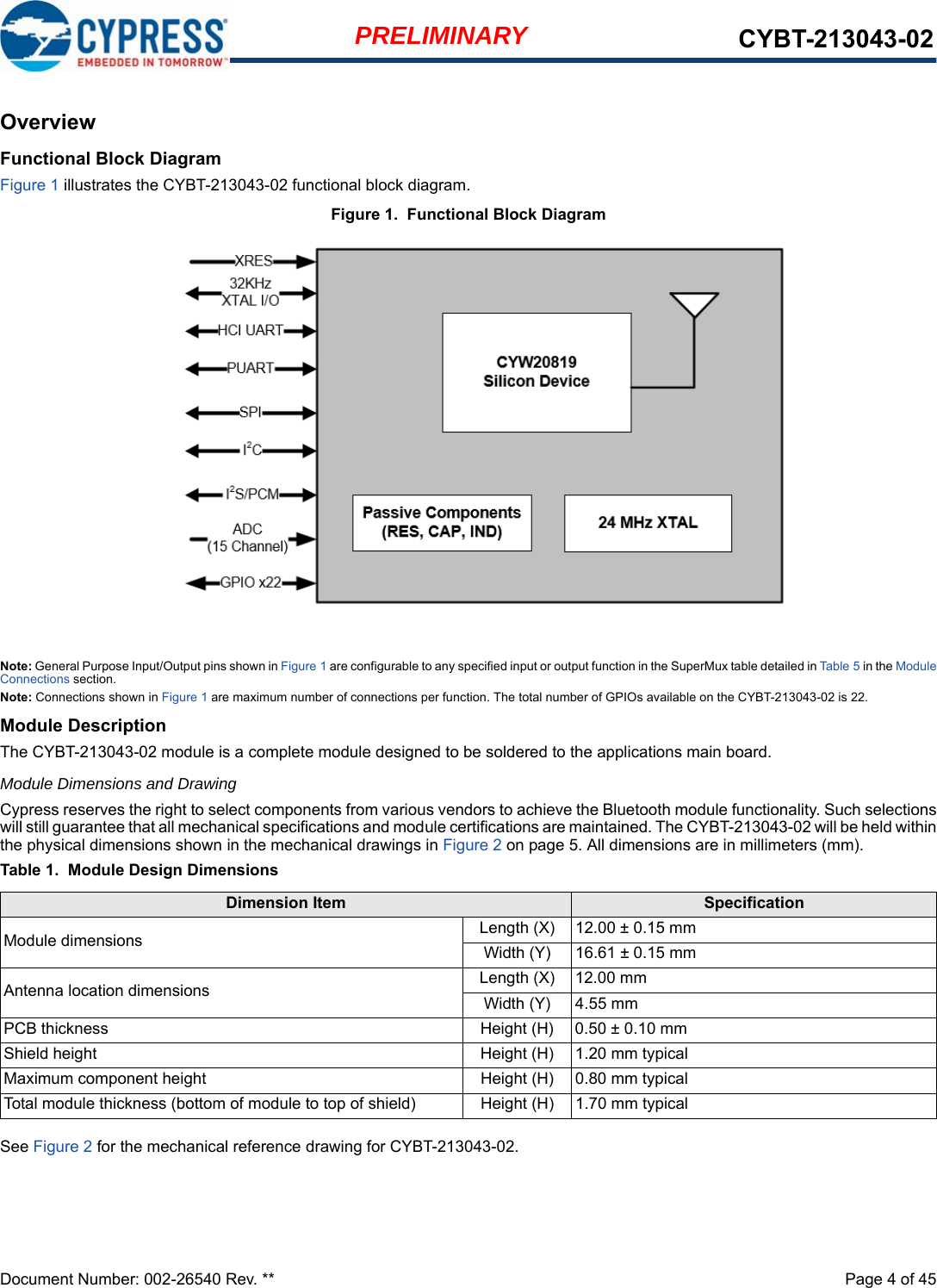
Cypress Semiconductor 3043 This product is a Bluetooth wireless EZ-BT WICED Module User Manual CYBT 013033 01 EZ BT Module
Cypress Semiconductor This product is a Bluetooth wireless EZ-BT WICED Module CYBT 013033 01 EZ BT Module
CYBT-213043-02_User Manual
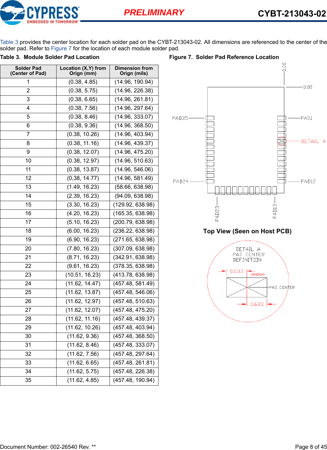
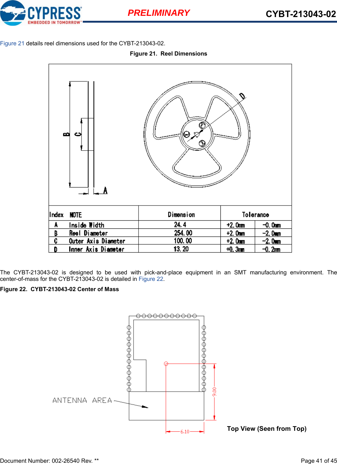
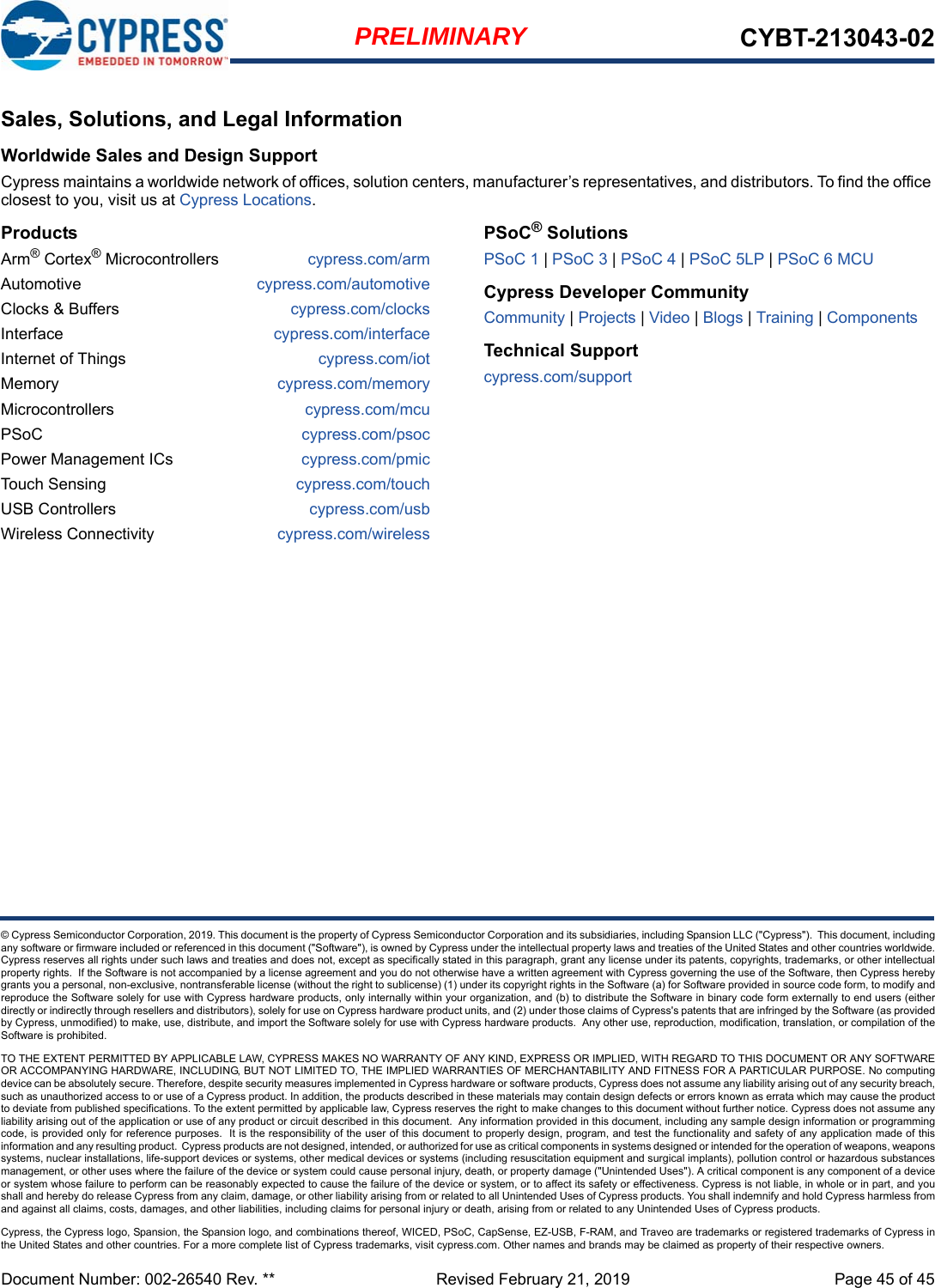
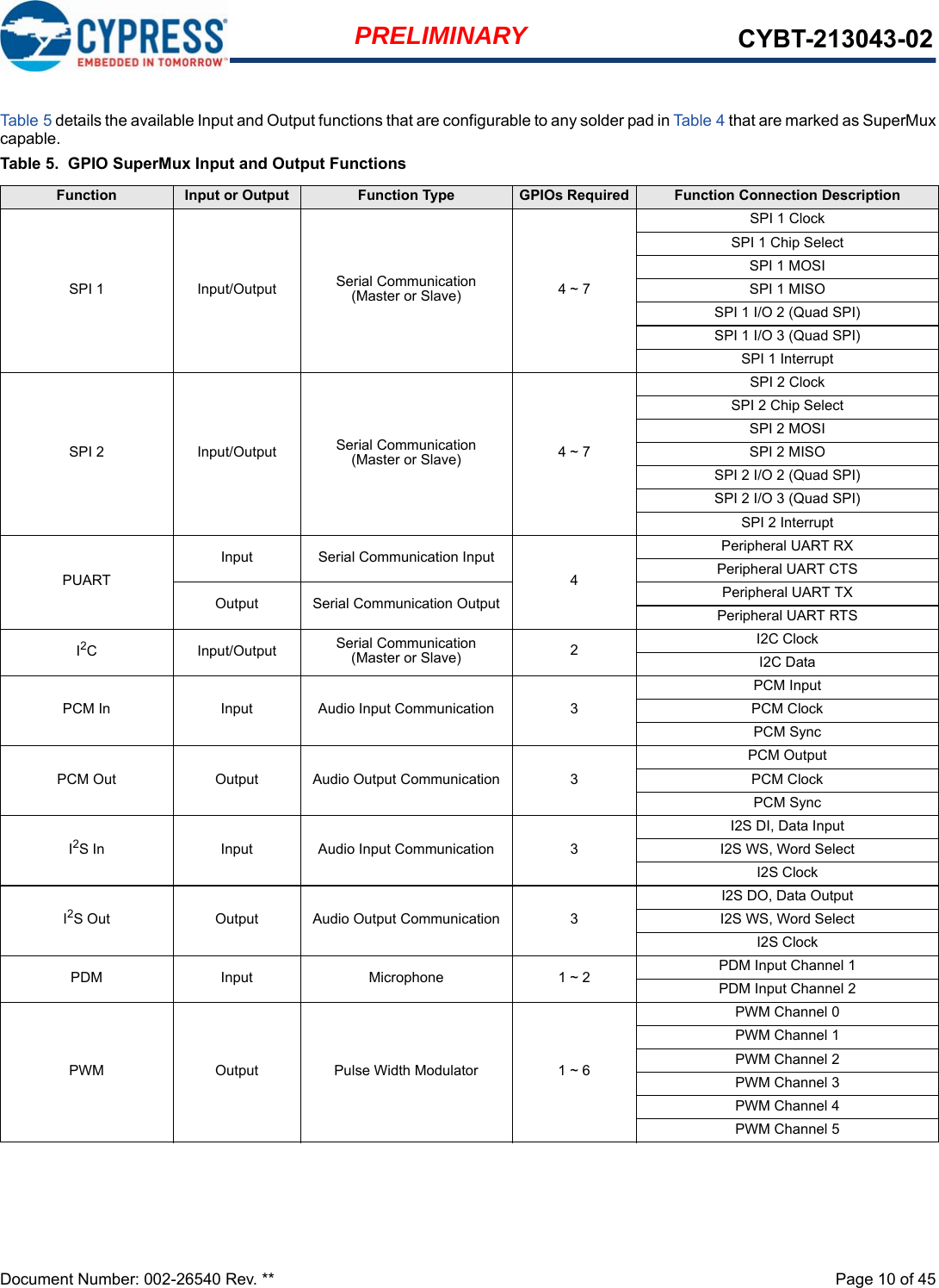
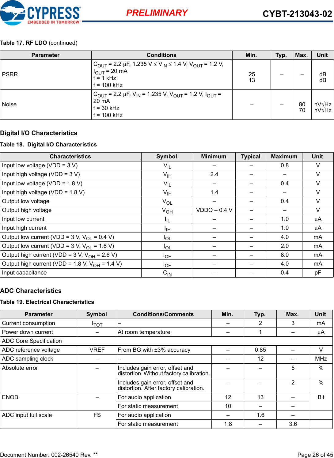
![Document Number: 002-26540 Rev. ** Page 9 of 45PRELIMINARY CYBT-213043-02Module ConnectionsTable 4 details the solder pad connection definitions and available functions for each connection pad. The GPIO connections availableon the CYBT-213043-02 can be configured to any of the input or output functions listed in Table 5. Table 4 specifies any function thatis required to be used on a specific solder pad, and also identifies SuperMux capable GPIOs that can be configured using theModusToolbox device configurator. Table 4. CYBT-213043-02 Solder Pad Connection Definitions Pad Pad Name Silicon Pin Name XTALI/O ADC GPIO SuperMux Capable[2]1 GND GND Ground2 VDD VDDIO Power Supply Input (1.71V ~ 3.63V)3 XRES RST_N External Reset (Active Low)4 P29 P29 - IN10 ✓✓ see Table 55P32 P32 - IN7 ✓✓ see Table 56P27 P27 - - ✓✓ see Table 57P37 P37 - IN2 ✓✓ see Table 58P28 P28 - IN11 ✓✓ see Table 59P0 P0 - IN29 ✓✓ see Table 510 P1 P1 - IN28 ✓✓ see Table 511 P10 P10 - IN25 ✓✓ see Table 512 P13 P13 - IN22 ✓✓ see Table 513 GND GND Ground14 P12 P12 - IN23 ✓✓ see Table 515 P11 P11 - IN24 ✓✓ see Table 516 P9 P9 - IN26 ✓✓ see Table 517 P14 P14 - IN21 ✓✓ see Table 518 P17 P17 - IN18 ✓✓, see Table 519 P5 P5 - - ✓✓ see Table 520 P6 P6 - - ✓✓ see Table 521 P4 P4 - - ✓ ✓ see Table 522 P2 P2 - - ✓✓ see Table 523 P3 P3 - - ✓✓ see Table 524 XTALI_32K XTALI_32K External Oscillator Input (32KHz) -- -25 XTALO_32K XTALO_32K External Oscillator Output (32KHz) -- -26 P15 P15 - IN20 ✓✓ see Table 527 P8 P8 - IN27 ✓✓ see Table 528 UART_CTS_N UART_CTS_N UART (HCI UART) Clear To Send Input Only29 UART_RTS_N UART_RTS_N UART (HCI UART) Request To Send Output Only30 UART_TXD UART_TXD UART (HCI UART) Transmit Data Only31 UART_RXD UART_RXD UART (HCI UART) Receive Data Only32 HOST_WAKE HOST_WAKE A signal from the CYBT-213043-02 module to the host indicating that the Bluetooth device requires attention.33 DEV_WAKE DEV_WAKE A signal from the host to the CYBT-213043-02 module indicating that the host requires attention.34 P26 P26 - - ✓✓ see Table 535 GND GND GroundNote2. The CYBT-213043-02 can configure GPIO connections to any Input/Output function described in Table 5 using the ModusToolbox Device Configurator.](https://usermanual.wiki/Cypress-Semiconductor/3043/User-Guide-4206267-Page-9.png)
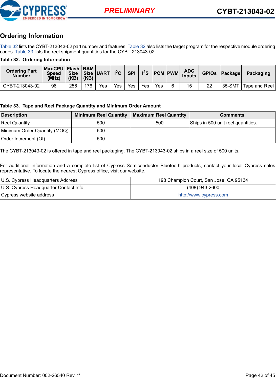
![Document Number: 002-26540 Rev. ** Page 24 of 45PRELIMINARY CYBT-213043-02Current ConsumptionTable 14 provides the current consumption measurements taken at the input of LDOIN and VDDIO combined (LDOIN = VDDIO =3.0 V).Silicon Core Buck RegulatorTable 14. Current ConsumptionOperational Mode Conditions Typical UnitHCI 48 MHz with Pause 1.3mA48 MHz without Pause 2.55RX Continuous RX 5.9TX Continuous TX - 4 dBm 5.8PDS – 16.5AePDS All RAM retained 8.7HID-Off (SDS) 32 kHz XTAL on 1.75Table 15. Core Buck RegulatorParameter Conditions Min. Typ. Max. UnitInput Supply, VBAT DC Range 1.62 3.0 3.63 VOutput Current Active Mode – < 60 100 mAPDS Mode – < 60 70Output VoltageActive Mode 1.1 1.26 1.4VPDS Mode, 40 mV min regulation window. 0.76 0.94 Avg(0.92-0.96) 1.4Output Voltage AccuracyActive Mode, includes line and load regulation.Before trim:After trim:–4–2 –+4+2 %%Ripple VoltageActive Mode2.2 H ± 25% inductor, DCR = 114 m ± 20%4.7 F ± 10% capacitor, Total ESR < 20 m –3–mVPDS Mode 40 40 –Output Inductor, LComponents are included on module. 1.6[3] 2.2 – HOutput Capacitor, COUT 3.0[3] 4.7 – FInput Capacitor, CIN 4.0[3] 10 –Input Supply Voltage Ramp Time 0 to 3.3 V 40 – – sNote3. Minimum values represent minimums after derating due to tolerance, temperature, and voltage effects.](https://usermanual.wiki/Cypress-Semiconductor/3043/User-Guide-4206267-Page-24.png)
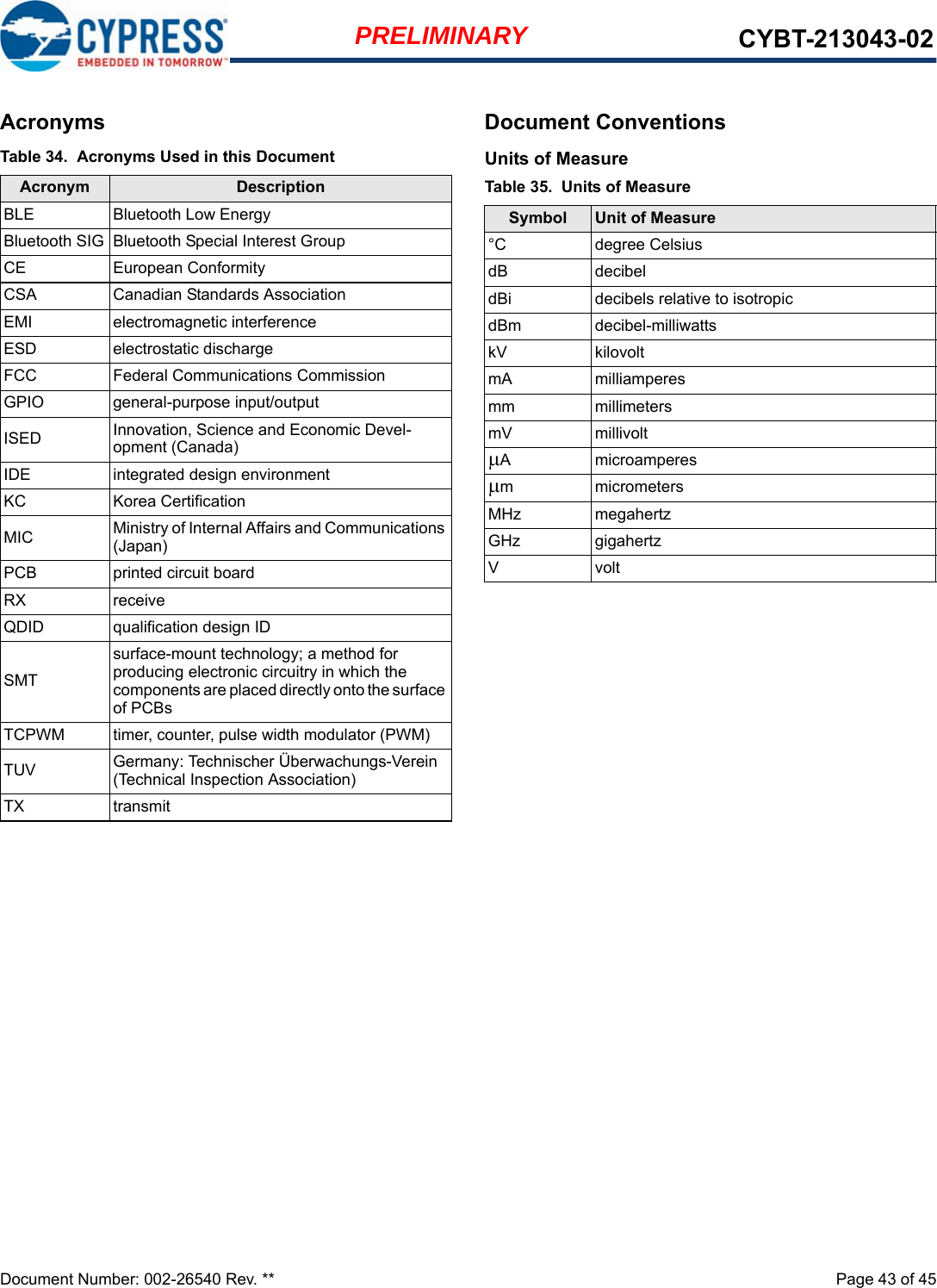
![Document Number: 002-26540 Rev. ** Page 25 of 45PRELIMINARY CYBT-213043-02Digital LDORF LDOTable 16. Digital LDOParameter Condition Min Typ Max UnitInput Supply, DIGLDO_VDDIN Min must be met for correct operation VOUT + 20 mV 1.26 1.4 VOutput Voltage, DIGLDO_VDDOUTRange 0.9 1.2 1.275Step – 25 – mVAccuracy after trimming –2 – +2 %Dropout Voltage At max load current – – 20 mVOutput Current DC Load 0.075 40 60 mAQuiescent Current At T 85 C, VIN = 1.4 V – – 40 AOutput Load Capacitor, COUT Total trace + cap ESR must be < 80 m¶1.55[4] 2.2 – FLine Regulation 1.235 V VIN 1.4 V – 5 10 mV/VLoad Regulation VOUT = 1.2 V, VIN = 1.26 V, 1 mA IOUT 25 mA – – 0.44 mV/mALoad Step Error IOUT step 1 mA 20 mA @ 1 s rise/fall, COUT = 2.2 F, VIN = 1.235 V, VOUT = 1.2 V –24 – +24 mVLeakage Current Power down Mode, VIN = 1.4 V, Temp = 25 C––50nAPower down Mode, VIN = 1.4 V, Temp = 125 C––2AIn-rush Current COUT = 2.2 F, VIN = 1.4 V, VOUT = 1.2 V – – 100 mALDO Turn On Time COUT = 2.2 F, VIN = 1.4 V, VOUT = 1.2 V, IOUT = 20 mA – – 120 sPSRRCOUT = 2.2 F, 1.235V VIN 1.4 V, VOUT = 1.2 V, IOUT = 20 mAf = 1 kHzf = 100 kHz2513 ––dBdBNote4. Minimum values represent minimums after derating due to tolerance, temperature, and voltage effects.Table 17. RF LDOParameter Conditions Min. Typ. Max. UnitInput Supply, RFLDO_VDDIN Min must be met for correct operation VOUT + 20 mV 1.26 1.4 VOutput Voltage, RFLDO_VDDOUTRange 1.1 1.2 1.275Step – 25 – mVAccuracy after trimming –2 – +2 %Dropout Voltage At max load current – – 20 mVOutput Current DC Load 0.075 20 60 mAQuiescent Current At T 85 C, VIN = 1.4 V – – 40 AOutput Load Capacitor, COUT Total trace + cap ESR must be < 80 m¶1.55[4] 2.2 – FLine Regulation 1.235 V VIN 1.4 V – 5 10 mV/VLoad Regulation VOUT = 1.2 V, VIN = 1.26 V, 1 mA IOUT 25 mA – – 0.44 mV/mALoad Step Error IOUT step 1 mA 20 mA @ 1 s rise/fall, COUT = 2.2 F, VIN = 1.235 V, VOUT = 1.2 V –24 – +24 mVLeakage Current Power down Mode, VIN = 1.4 V, Temp = 25 C––50nAPower down Mode, VIN = 1.4 V, Temp = 125 C––2AIn-rush Current COUT = 2.2 F, VIN = 1.4 V, VOUT = 1.2 V – – 100 mALDO Turn On Time COUT = 2.2 F, VIN = 1.4 V, VOUT = 1.2 V, IOUT = 20 mA – – 120 s](https://usermanual.wiki/Cypress-Semiconductor/3043/User-Guide-4206267-Page-25.png)
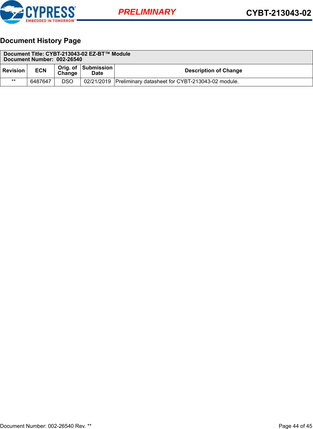
![Document Number: 002-26540 Rev. ** Page 27 of 45PRELIMINARY CYBT-213043-02Conversion rate –For audio application 816 –kHzFor static measurement 50 100 –Signal bandwidth –For audio application 20 –8K HzFor static measurement –DC –Input impedance RIN For audio application 10 – – KWFor static measurement 500 – –Startup time –For audio application –10 –msFor static measurement –20 –sMIC PGA SpecificationsMIC PGA gain range – – 0 – 42 dBMIC PGA gain step – – – 1 – dBMIC PGA gain error – Includes part-to-part gain variation –1 – 1 dBPGA input referred noise – At 42 dB PGA gain A-weighted – – 4 VPassband gain flatness – PGA and ADC, 100 Hz–4 kHz –0.5 – 0.5 dBMIC Bias SpecificationsMIC bias output voltage – At 2.5-V supply – 2.1 – VMIC bias loading current – – – – 3 mAMIC bias noise – Refers to PGA input 20 Hz to 8 kHz, A-weighted ––3VMIC bias PSRR – at 1 kHz 40 – – dBADC SNR – A-weighted 0 dB PGA gain 78 – – dBADC THD + N – –3 dBFS input 0 dB PGA gain 74 – – dBGPIO input voltage Always lower than avddBAT – – 3.6 VGPIO source impedance[5] – Resistance – – 1 kCapacitance – – 10 pFNote5. Conditional requirement for the measurement time of 10 s. Relaxed with longer measurement time for each GPIO input channel.Table 19. Electrical Characteristics (continued)Parameter Symbol Conditions/Comments Min. Typ. Max. Unit](https://usermanual.wiki/Cypress-Semiconductor/3043/User-Guide-4206267-Page-27.png)
![Document Number: 002-26540 Rev. ** Page 28 of 45PRELIMINARY CYBT-213043-02Chipset RF SpecificationsTable 20, Table 21, Table 22, and Table 23 apply to single-ended industrial temperatures. Unused inputs are left open.Table 20. BR/EDR - Receiver RF SpecificationsParameter Mode and Conditions Min Typ Max UnitReceiver SectionFrequency range – 2402 – 2480 MHzRX sensitivityGFSK, BDR GFSK 0.1% BER, 1 Mbps – –92[] –dBmEDR 2M – –93.5 – dBEDR 3M – –87 –Maximum input – –20 – – dBmInterference PerformanceC/I cochannel GFSK, BDR GFSK 0.1% BER[] ––11.0 dBC/I 1 MHz adjacent channel GFSK, BDR GFSK 0.1% BER[] ––0.0C/I 2 MHz adjacent channel GFSK, BDR GFSK 0.1% BER[] – – –30.0C/I 3 MHz adjacent channel GFSK, BDR GFSK 0.1% BER[] – – –40.0C/I image channel GFSK, BDR GFSK 0.1% BER[] –––9.0C/I 1 MHz adjacent to image channel GFSK, BDR GFSK 0.1% BER[] – – –20.0Out-of-Band Blocking Performance (CW)[]30 MHz to 2000 MHz BDR GFSK 0.1% BER – –10.0 –dBm2000 MHz to 2399 MHz BDR GFSK 0.1% BER – –27 –2498 MHz to 3000 MHz BDR GFSK 0.1% BER – –27 –3000 MHz to 12.75 GHz BDR GFSK 0.1% BER – –10.0 –Intermodulation Performance[]BT, interferer signal level BDR GFSK 0.1% BER – – –39.0 dBmSpurious Emissions30 MHz to 1 GHz – – – –57.0 dBm1 GHz to 12.75 GHz – – – –55.0. Notes6. The receiver sensitivity is measured at BER of 0.1% on the device interface with dirty TX Off.7. Desired signal is 10 dB above the reference sensitivity level (defined as –70 dBm).8. Desired signal is 3 dB above the reference sensitivity level (defined as –70 dBm).9. Desired signal is –64 dBm Bluetooth-modulated signal, interferer 1 is –39 dBm sine wave at frequency f1, interferer 2 is –39 dBm Bluetooth-modulated signal at frequency f2, f0 = 2 * f1 – f2, and |f2 – f1| = n * 1 MHz, where n = 3, 4, or 5. For the typical case, n = 4.](https://usermanual.wiki/Cypress-Semiconductor/3043/User-Guide-4206267-Page-28.png)
![Document Number: 002-26540 Rev. ** Page 29 of 45PRELIMINARY CYBT-213043-02Table 21. BR/EDR - Transmitter RF SpecificationsParameter Min Typ Max UnitTransmitter SectionFrequency range 2402 – 2480 MHzClass 2: BR TX power – 4.0 – dBmClass 2: EDR 2M and 3M TX power – 0 –20 dB bandwidth – 930 1000 kHzAdjacent Channel Power|M – N| = 2 – – –20 dBm|M – N| 3 [10] – – –40Out-of-Band Spurious Emission30 MHz to 1 GHz – – –36.0dBm1 GHz to 12.75 GHz – – –30.01.8 GHz to 1.9 GHz – – –47.0 5.15 GHz to 5.3 GHz – – –47.0 LO PerformanceInitial carrier frequency tolerance –75 – +75 kHzFrequency DriftDH1 packet –25 – +25kHzDH3 packet –40 – +40DH5 packet –40 – +40Drift rate –20 – 20 kHz/50 µsFrequency DeviationAverage deviation in payload (sequence used is 00001111) 140 – 175 kHzMaximum deviation in payload (sequence used is 10101010) 115 – – Channel spacing – 1 – MHzNote10. Meet SIG Specification.Table 22. BLE RF SpecificationsParameter Conditions Minimum Typical Maximum UnitFrequency range N/A 2402 – 2480 MHzRX sensitivity[11] GFSK, BDR GFSK 0.1% BER 0.1% BER, 1 Mbps ––95–dBmTX power N/A – 4.0 –Mod Char: Delta F1 average N/A 225 255 275 kHzMod Char: Delta F2 max[12] N/A 99.9 – – %Mod Char: Ratio N/A 0.8 – – %Notes11. Dirty TX is Off.12. At least 99.9% of all delta F2 max frequency values recorded over 10 packets must be greater than 185 kHz.](https://usermanual.wiki/Cypress-Semiconductor/3043/User-Guide-4206267-Page-29.png)
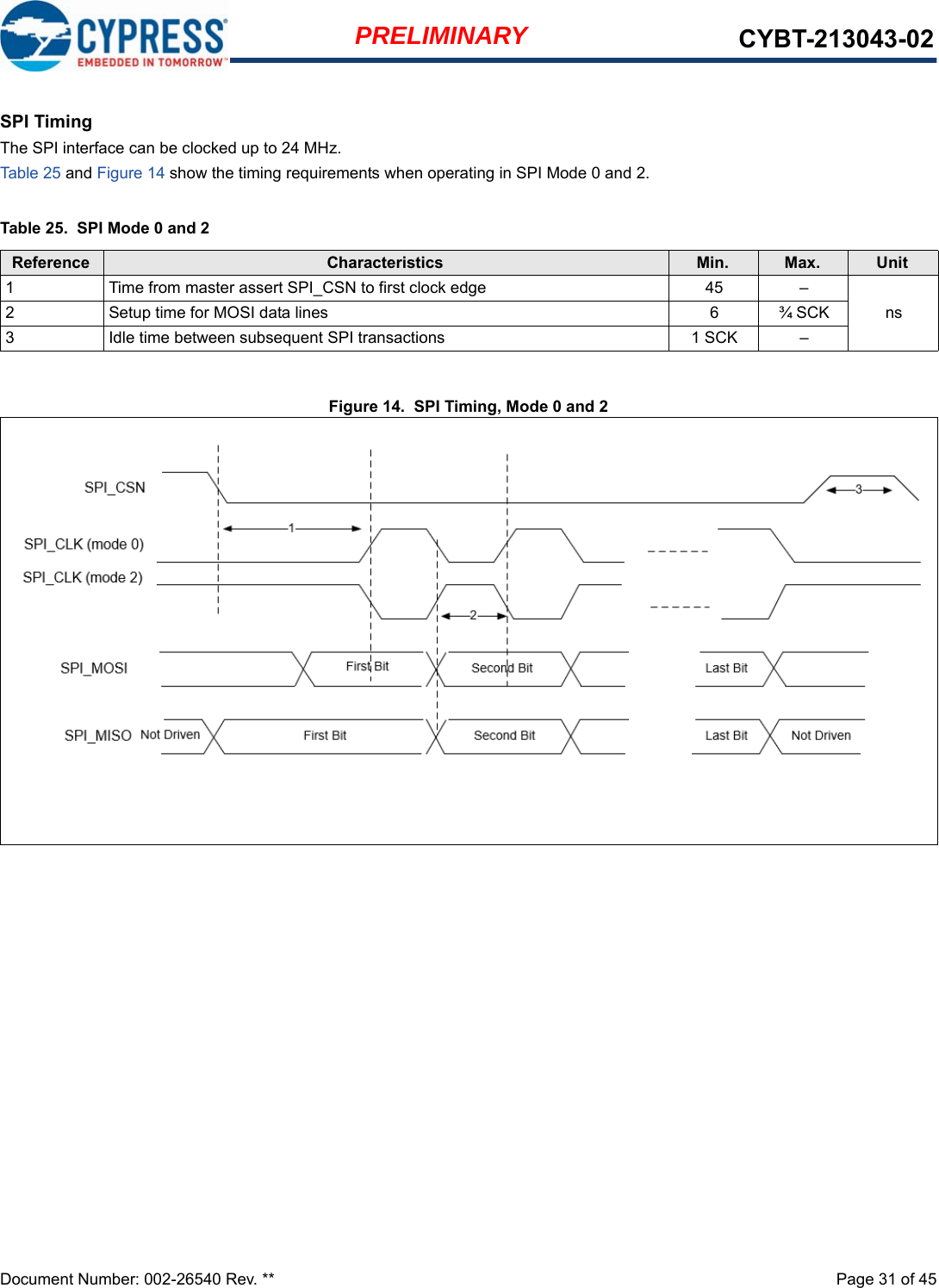
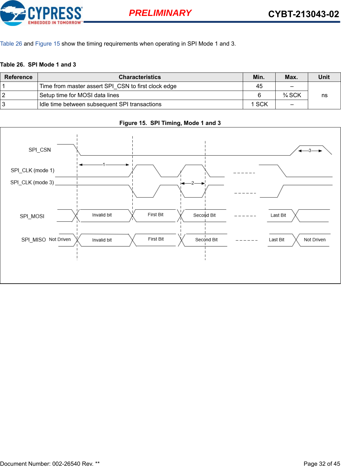
![Document Number: 002-26540 Rev. ** Page 30 of 45PRELIMINARY CYBT-213043-02Timing and AC CharacteristicsIn this section, use the numbers listed in the Reference column of each table to interpret the following timing diagrams.UART TimingFigure 13. UART TimingTable 23. BLE2 RF SpecificationsParameter Conditions Minimum Typical Maximum UnitRX sensitivity[13] –––89–dBmTX power – – 4.0 –Note13. 255 packet.Table 24. UART Timing SpecificationsReference Characteristics Min. Typ. Max. Unit1 Delay time, UART_CTS_N low to UART_TXD valid. – – 1.50 Bit periods2 Setup time, UART_CTS_N high before midpoint of stop bit. – – 0.67 Bit periods3 Delay time, midpoint of stop bit to UART_RTS_N high. – – 1.33 Bit periods](https://usermanual.wiki/Cypress-Semiconductor/3043/User-Guide-4206267-Page-30.png)
![Document Number: 002-26540 Rev. ** Page 33 of 45PRELIMINARY CYBT-213043-02I2C Compatible Interface TimingThe specifications in Table 26 references Figure .Figure 16. I2C Interface Timing DiagramTable 27. I2C Interface Timing Specifications (up to 1 MHz)Reference Characteristics Minimum Maximum Unit1 Clock frequency –100kHz40080010002 START condition setup time 650 –ns3 START condition hold time 280 –4 Clock low time 650 –5 Clock high time 280 –6 Data input hold time[14] 0 –7 Data input setup time 100 –8 STOP condition setup time 280 –9 Output valid from clock – 400 10 Bus free time[15] 650 –Notes14. As a transmitter, 125 ns of delay is provided to bridge the undefined region of the falling edge of SCL to avoid unintended generation of START or STOP conditions.15. Time that the CBUS must be free before a new transaction can start.](https://usermanual.wiki/Cypress-Semiconductor/3043/User-Guide-4206267-Page-33.png)
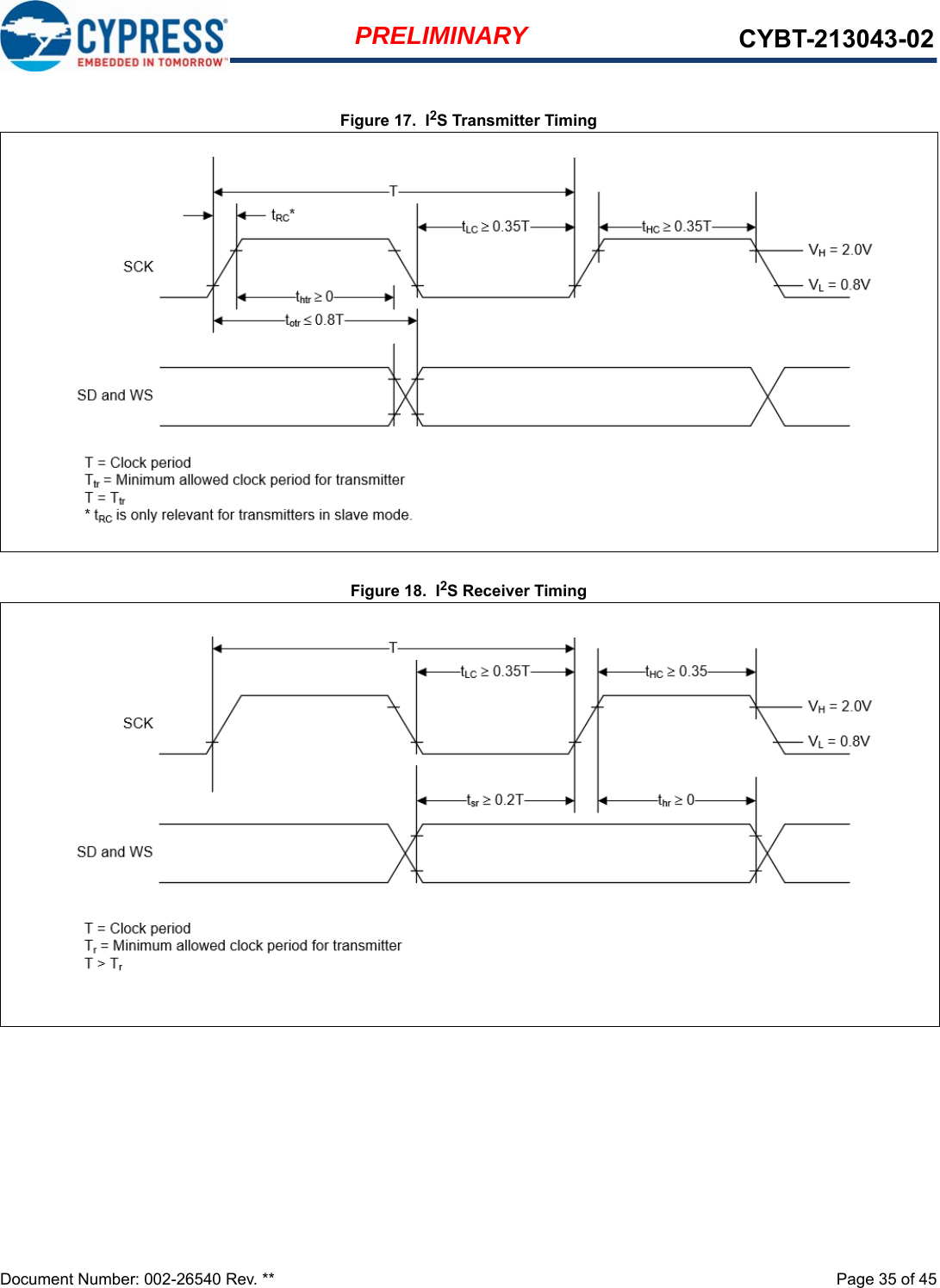
![Document Number: 002-26540 Rev. ** Page 34 of 45PRELIMINARY CYBT-213043-02I2S Interface TimingI2S timing is shown below in Table 28, Figure 17, and Figure 18.Table 28. Timing for I2S Transmitters and ReceiversTransmitter ReceiverNotesLower LImit Upper Limit Lower Limit Upper LimitMin Max Min Max Min Max Min MaxClock Period T Ttr –––Tr–––[16]Master Mode: Clock generated by transmitter or receiverHIGH tHC 0.35Ttr – – – 0.35Ttr – – – [17]LOWtLC 0.35Ttr – – – 0.35Ttr – – – [17]Slave Mode: Clock accepted by transmitter or receiverHIGH tHC –0.35Ttr –––0.35Ttr ––[16]LOW tLC –0.35Ttr –––0.35Ttr ––[16]Rise time tRC – – 0.15Ttr – – – – [17]TransmitterDelay tdtr – – – 0.8T – – – – [18]Hold time thtr 0–––––––[17]ReceiverSetup time tsr ––––0.2Ttr – – – [19]Hold time thr ––––0.2Ttr – – – [19]Notes16. The system clock period T must be greater than Ttr and Tr because both the transmitter and receiver have to be able to handle the data transfer rate.17. At all data rates in master mode, the transmitter or receiver generates a clock signal with a fixed mark/space ratio. For this reason, tHC and tLC are specified with respect to T.18. In slave mode, the transmitter and receiver need a clock signal with minimum HIGH and LOW periods so that they can detect the signal. So long as the minimum periods are greater than 0.35Tr, any clock that meets the requirements can be used.19. Because the delay (tdtr) and the maximum transmitter speed (defined by Ttr) are related, a fast transmitter driven by a slow clock edge can result in tdtr not exceeding tRC which means thtr becomes zero or negative. Therefore, the transmitter has to guarantee that thtr is greater than or equal to zero, so long as the clock rise-time tRC is not more than tRCmax, where tRCmax is not less than 0.15Ttr.20. To allow data to be clocked out on a falling edge, the delay is specified with respect to the rising edge of the clock signal and T, always giving the receiver sufficient setup time.21. The data setup and hold time must not be less than the specified receiver setup and hold time.](https://usermanual.wiki/Cypress-Semiconductor/3043/User-Guide-4206267-Page-34.png)
![Document Number: 002-26540 Rev. ** Page 36 of 45PRELIMINARY CYBT-213043-02Environmental SpecificationsEnvironmental ComplianceThis Cypress BLE module is produced in compliance with the Restriction of Hazardous Substances (RoHS) and Halogen-Free (HF)directives. The Cypress module and components used to produce this module are RoHS and HF compliant.RF CertificationThe CYBT-213043-02 module is certified under the following RF certification standards:■FCC: WAP3034■ISED: 7922A-3034■MIC: TBD■CESafety CertificationThe CYBT-213043-02 module complies with the following safety regulations:■Underwriters Laboratories, Inc. (UL): Filing E331901■CSA■TUVEnvironmental ConditionsTable 29 describes the operating and storage conditions for the Cypress Bluetooth module.ESD and EMI ProtectionExposed components require special attention to ESD and electromagnetic interference (EMI).A grounded conductive layer inside the device enclosure is suggested for EMI and ESD performance. Any openings in the enclosurenear the module should be surrounded by a grounded conductive layer to provide ESD protection and a low-impedance path to ground. Device Handling: Proper ESD protocol must be followed in manufacturing to ensure component reliability.Table 29. Environmental Conditions for CYBT-213043-02Description Minimum Specification Maximum SpecificationOperating temperature 30 °C 85 °COperating humidity (relative, non-condensation) 5% 85%Thermal ramp rate – 10 °C/minuteStorage temperature –40 °C 85 °CStorage temperature and humidity – 85 °C at 85%ESD: Module integrated into system Components[22] –15 kV Air2.0 kV ContactNote22. This does not apply to the RF pins (ANT).](https://usermanual.wiki/Cypress-Semiconductor/3043/User-Guide-4206267-Page-36.png)