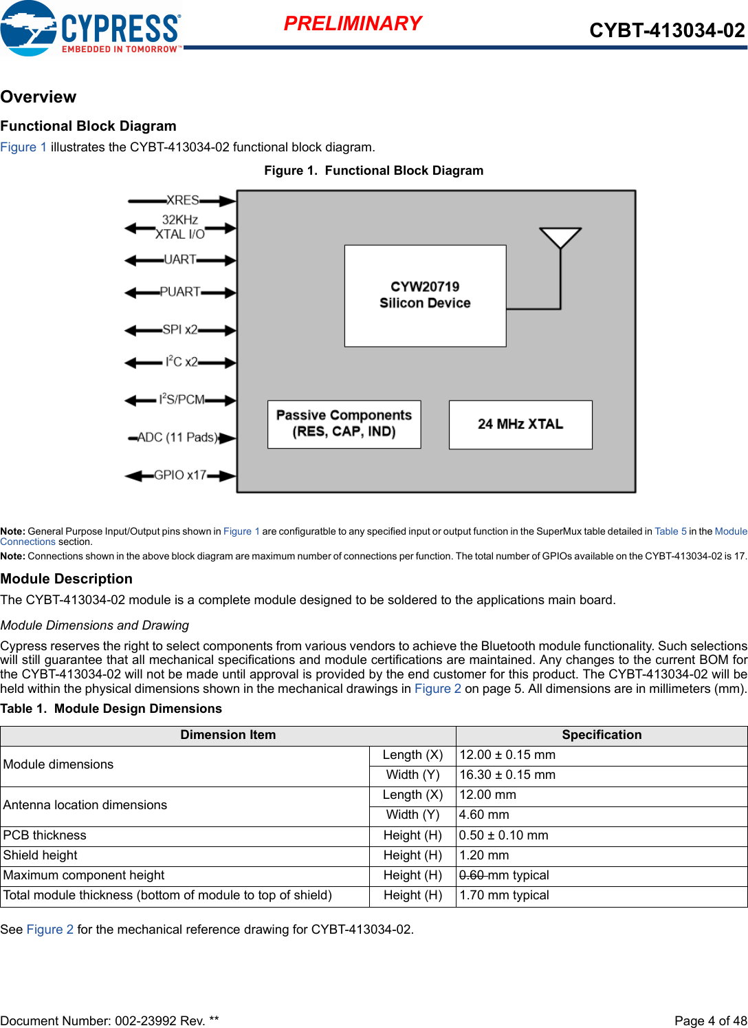
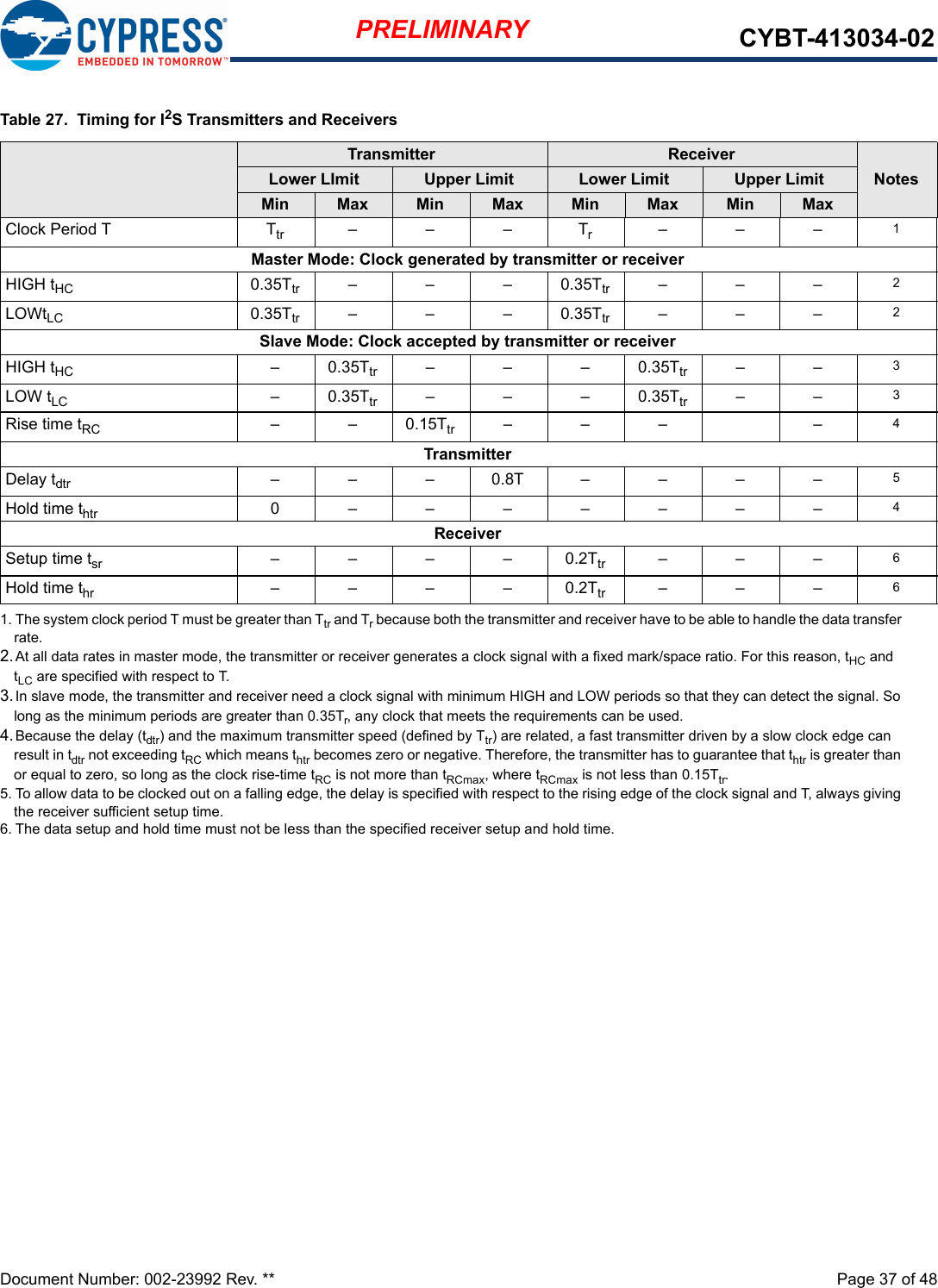
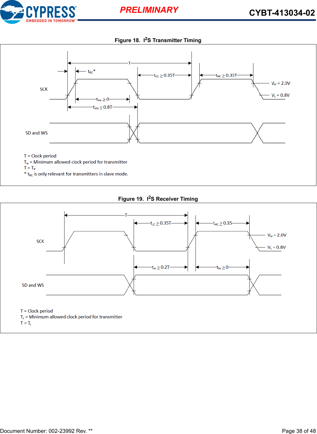
Cypress Semiconductor 3034 This product is a Bluetooth wireless EZ-BT WICED Module with Mesh User Manual CYBT 013033 01 EZ BT Module
Cypress Semiconductor This product is a Bluetooth wireless EZ-BT WICED Module with Mesh CYBT 013033 01 EZ BT Module
User Manual
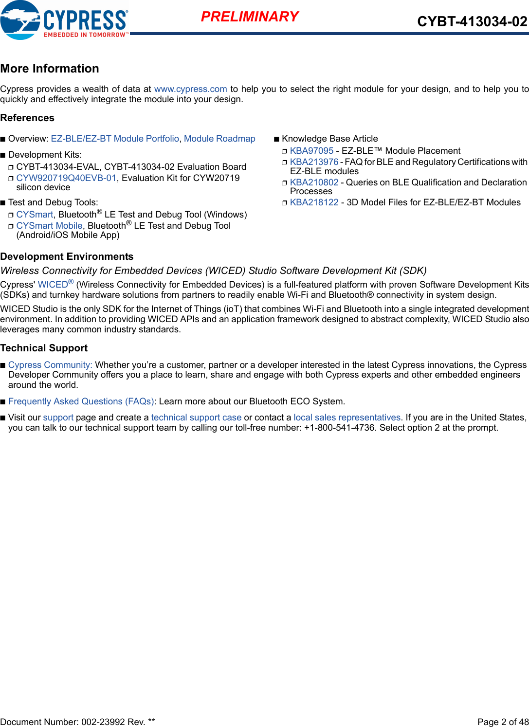
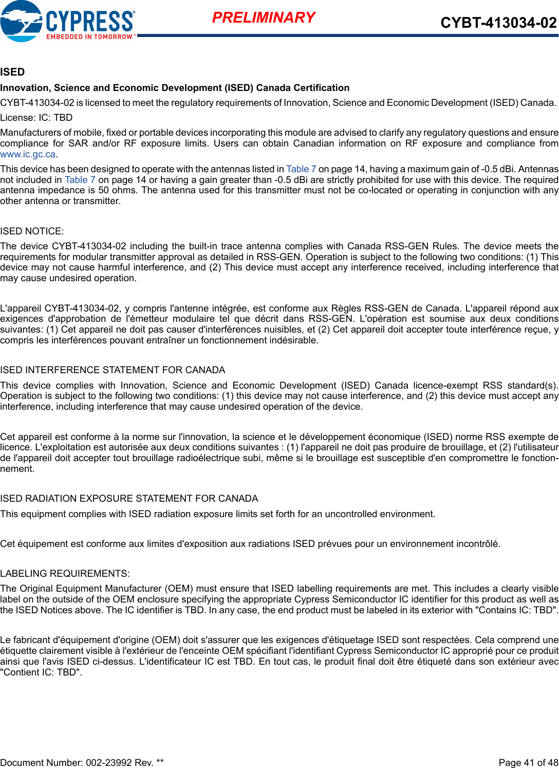
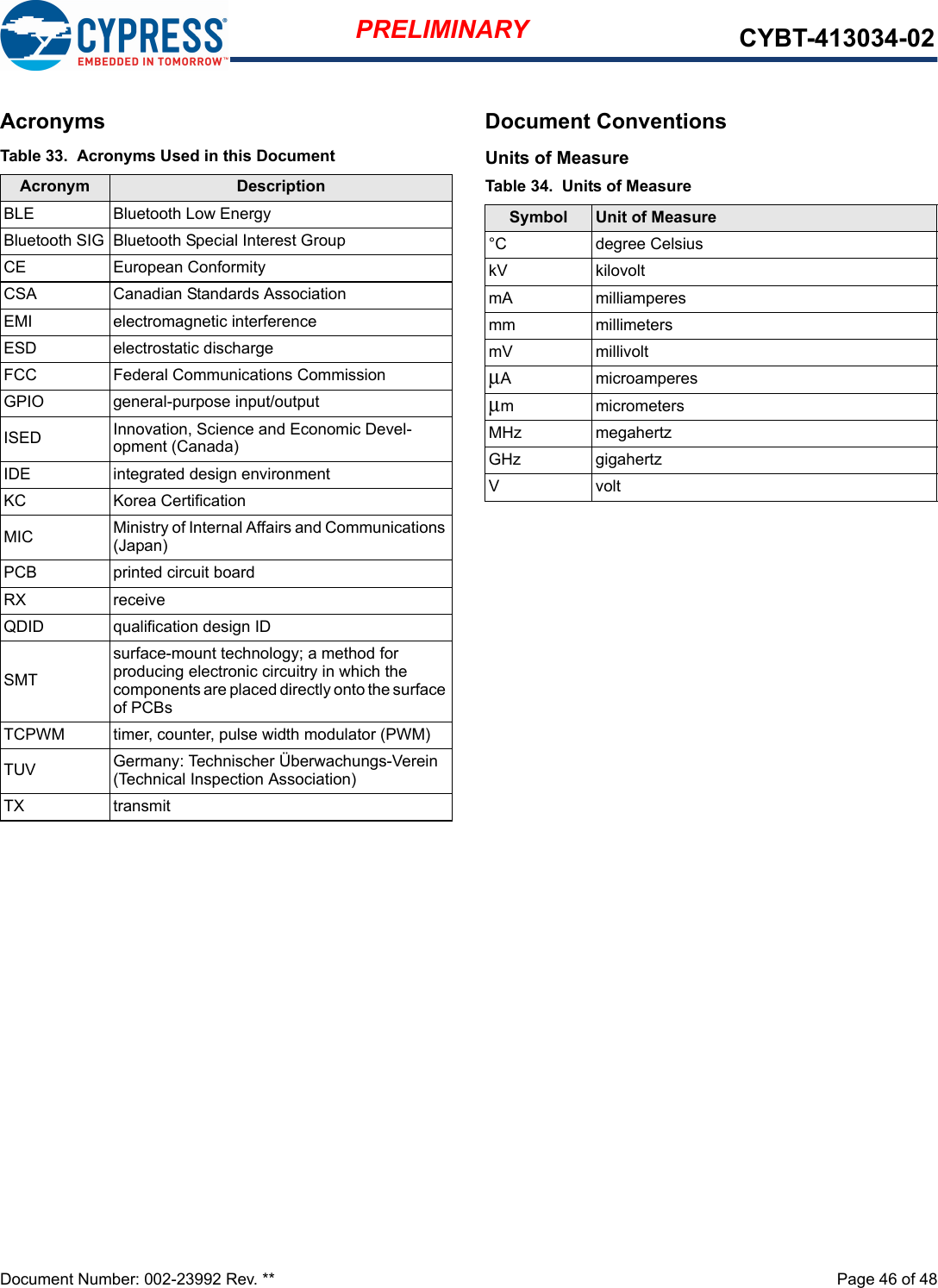
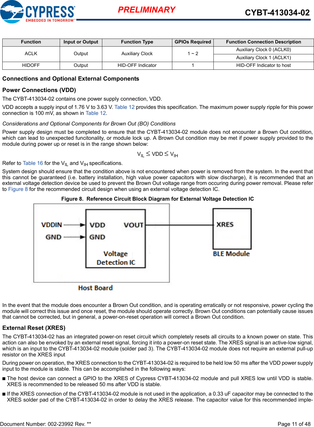
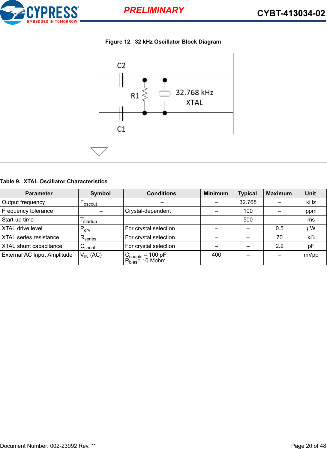
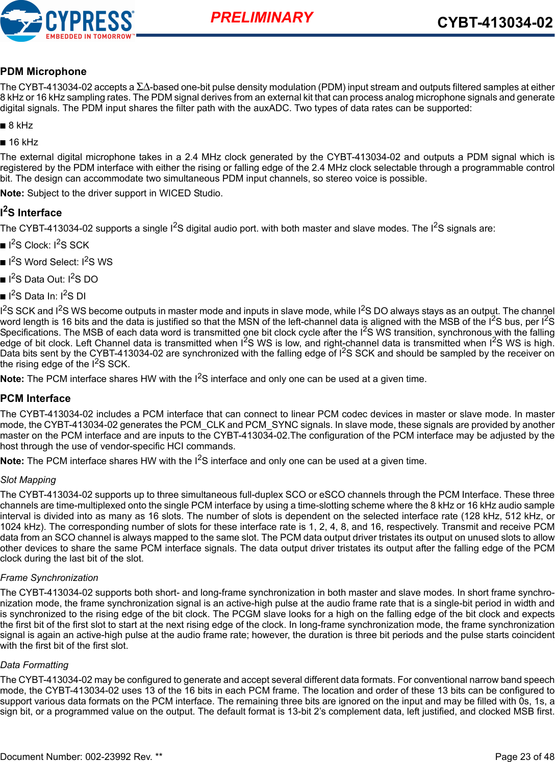
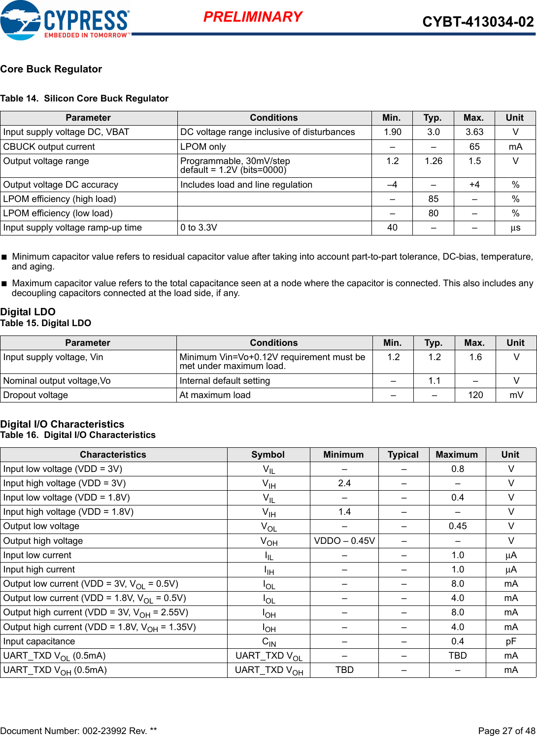
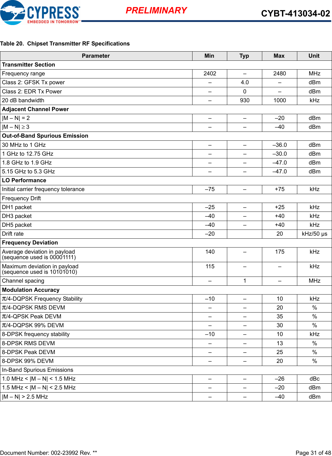
![Document Number: 002-23992 Rev. ** Page 9 of 48PRELIMINARY CYBT-413034-02Module ConnectionsTable 4 details the solder pad connection definitions and available functions for each connection pad. The GPIO connections availableon the CYBT-413034-02 can be configured to any of the input or output funcitons listed in Table 5. Table 4 specifies any function thatis required to be used on a specific solder pad, and also identifies GPIOs that can be configured using the SuperMux. Table 4. CYBT-413034-02 Solder Pad Connection DefinitionsTable 5 details the available Input and Ouput functions that are configurable to any sodler pad in Table 4 that are marked as SuperMuxcapable. Pad Pad Name Silicon Pin Name XTALI/O ADC GPIO SuperMux Capable[2]1 GND GND Ground2 VDD VDDIO Power Supply Input (1.76V ~ 3.63V)3 XRES RST_N External Reset (Active Low)4P25 P25 - - 33 see Table 55P33 P33 - IN6 33 see Table 56P26 P26 - - 33 see Table 57P38 P38 - IN1 33 see Table 58P1 P1 - IN28 33 see Table 59P0 P0 - IN29 33 see Table 510 P29 P29 - IN10 33 see Table 511 GND GND Ground12 P13/P23/P28 P13P23P28 -IN22 (P13)IN12 (P23)IN11 (P28)3(P13/P23/P28) 3 see Table 513 P17 P17 - IN18 33 see Table 514 P7 P7 - - 3-15 P4 P4 - - 3-16 P2 P2 - - 33 see Table 517 P16 P16 - IN19 3-18 XTALI_32K/P15[3] XTALI_32KP15 External Oscillator Input (32KHz) IN20 (P15) 3(P15) 3(P15), see Ta b le 519 P6 P6 - - 33 see Table 520 XTALO_32K XTALO_32K External Oscillator Output (32KHz) -- -21 P10/P11 P10P11 -IN25 (P10)IN24 (P11) 3 (P10/P11) 3 see Table 522 P34/P35/P36 P34P35P36 -IN5 (P34)IN4 (P35)IN3 (P36)3 (P34/P35/P36) 3 see Table 523 UART_CTS_N BT_UART_CTS_N UART (HCI UART) Clear To Send Input Only24 UART_RTS_N BT_UART_RTS_N UART (HCI UART) Request To Send Output Only25 UART_TXD BT_UART_TXD UART (HCI UART) Transmit Data Only26 UART_RXD BT_UART_RXD UART (HCI UART) Receive Data Only27 HOST_WAKE BT_HOST_WAKE A signal from the CYBT-423028-02 module to the host indicating that the Bluetooth device requires attention.28 GND GND Ground29 GND GND Ground30 GND GND GroundNote2. The CYBT-413034-02 can configure GPIO connections to any Input/Output function described in Table 5. 3. P15 should not be driven high externally while the part is held in reset (it can be floating or driven low). Failure to do so may cause some current to flow through P15 until the device comes out of reset.](https://usermanual.wiki/Cypress-Semiconductor/3034/User-Guide-3884229-Page-9.png)
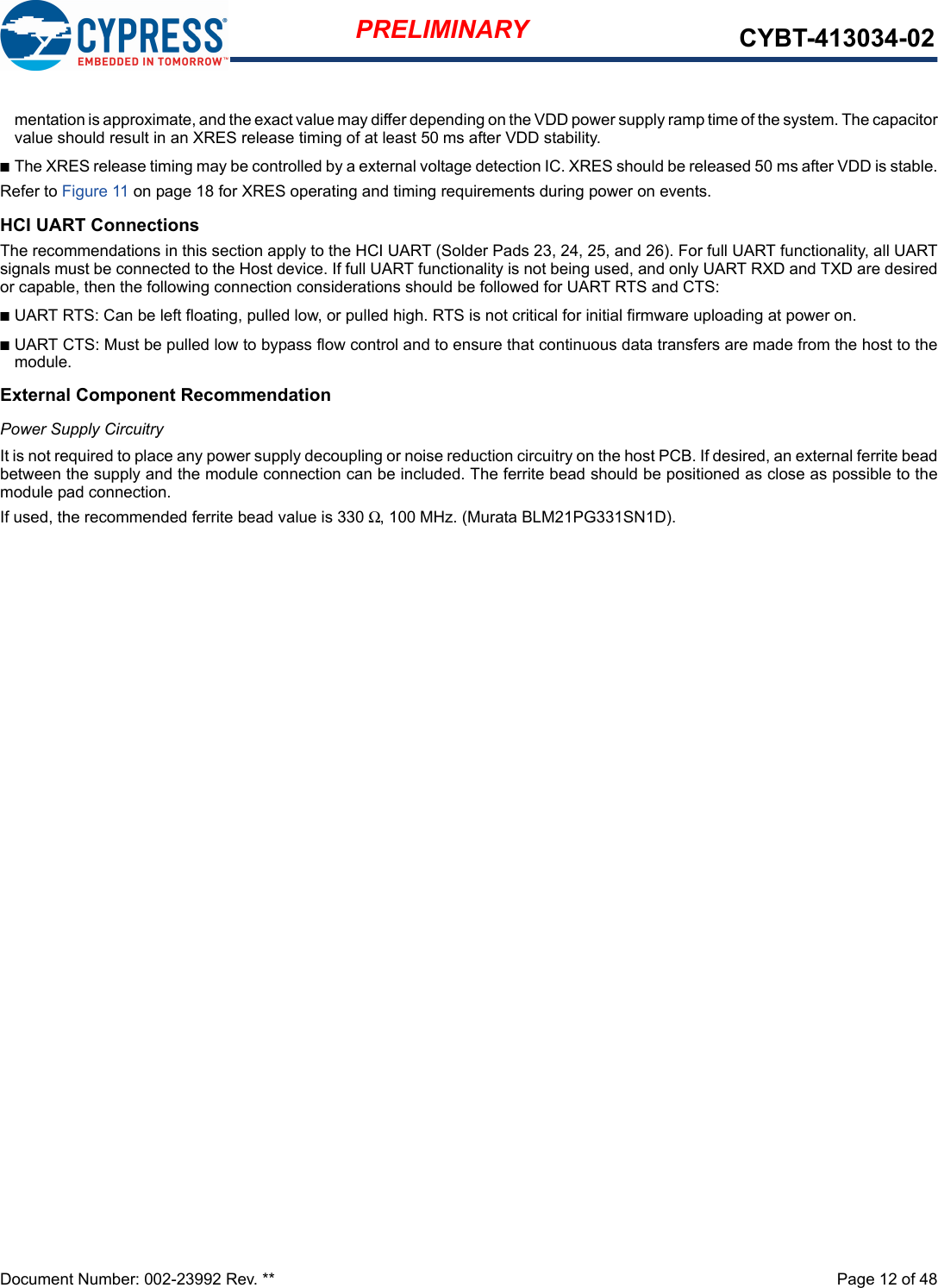
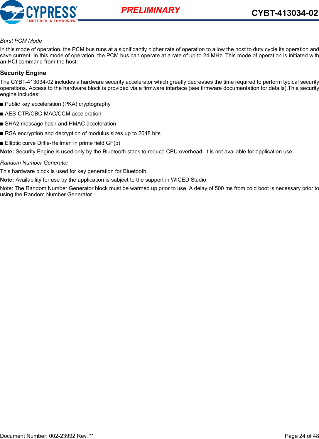
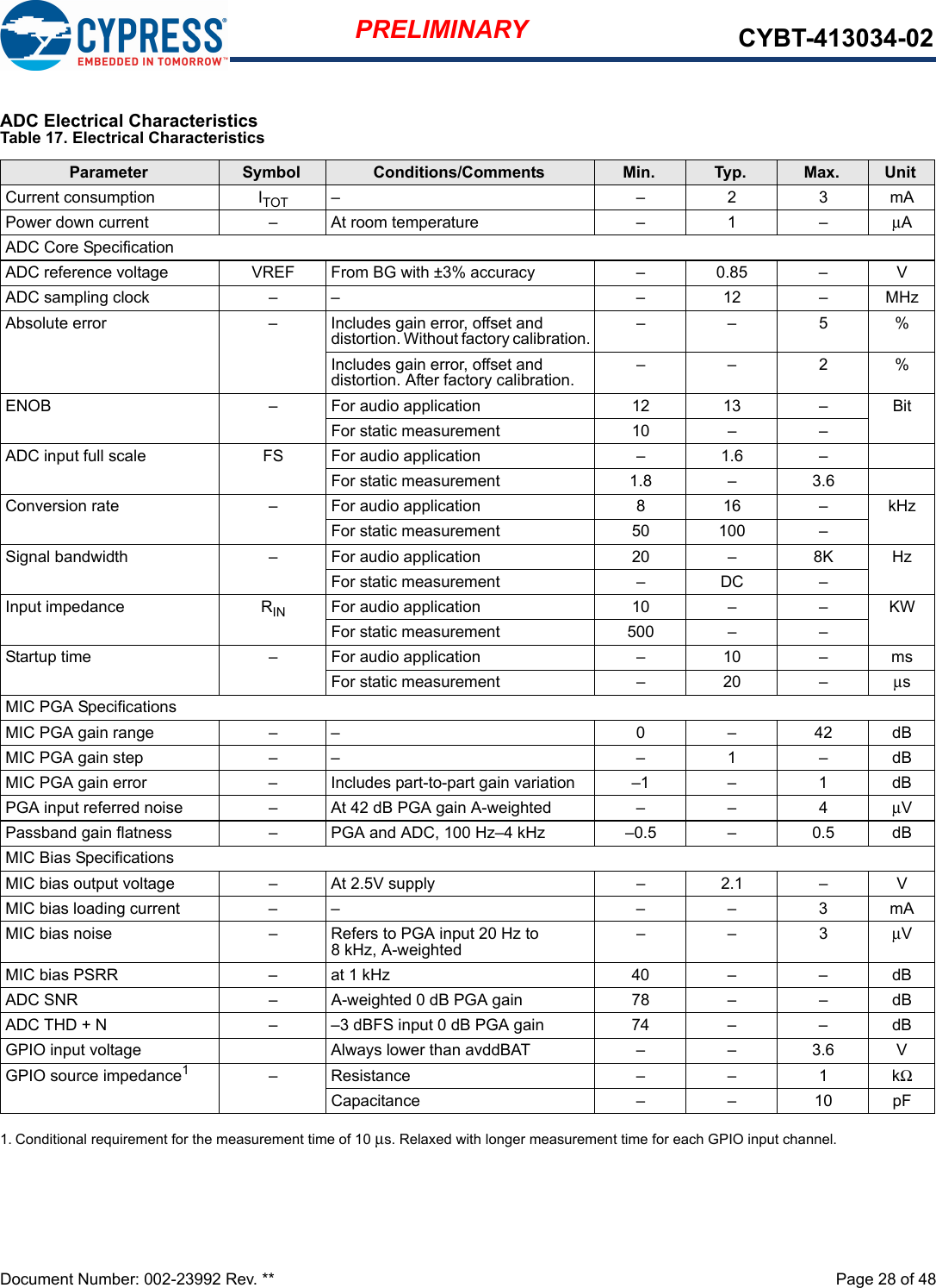
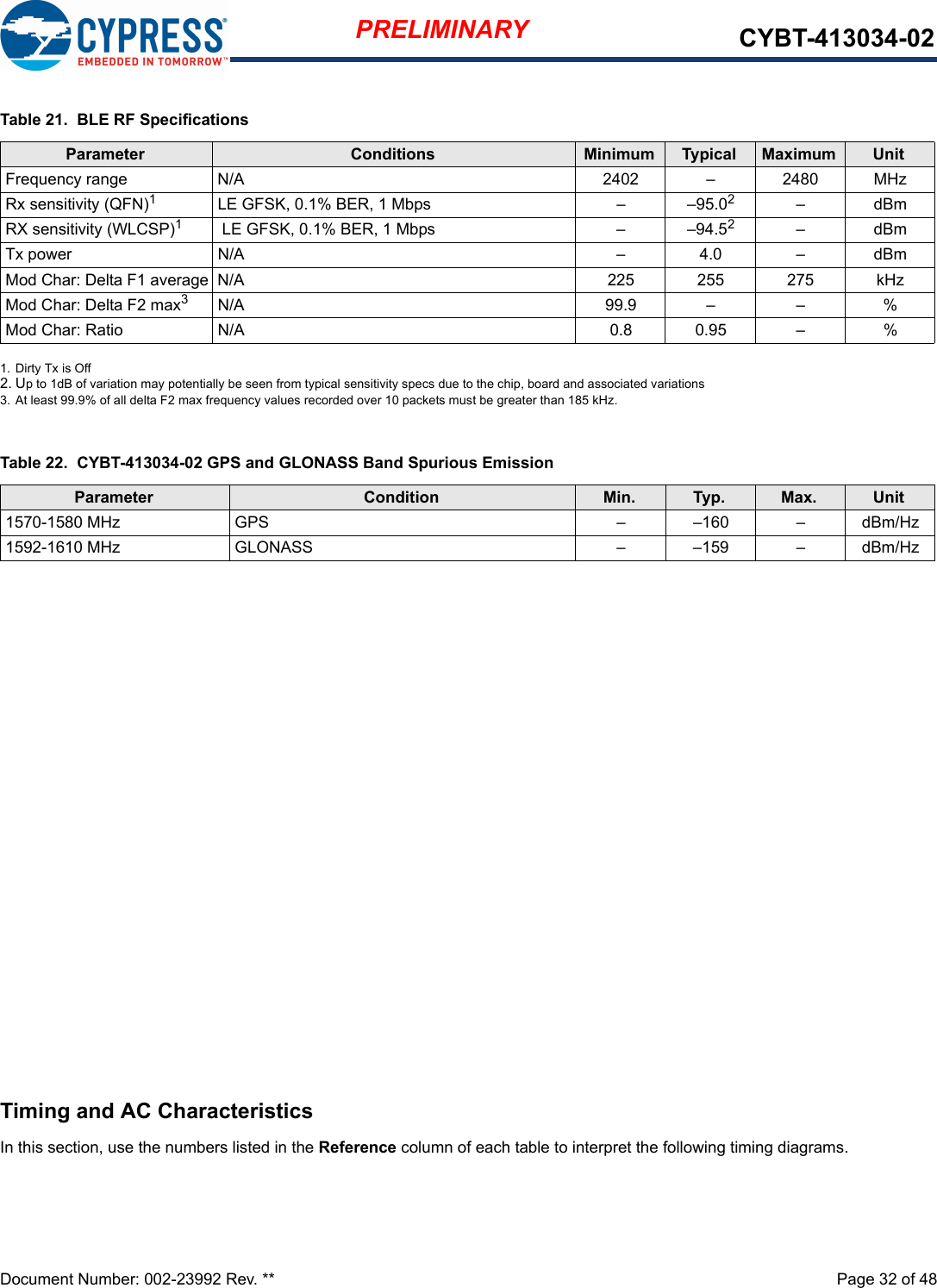
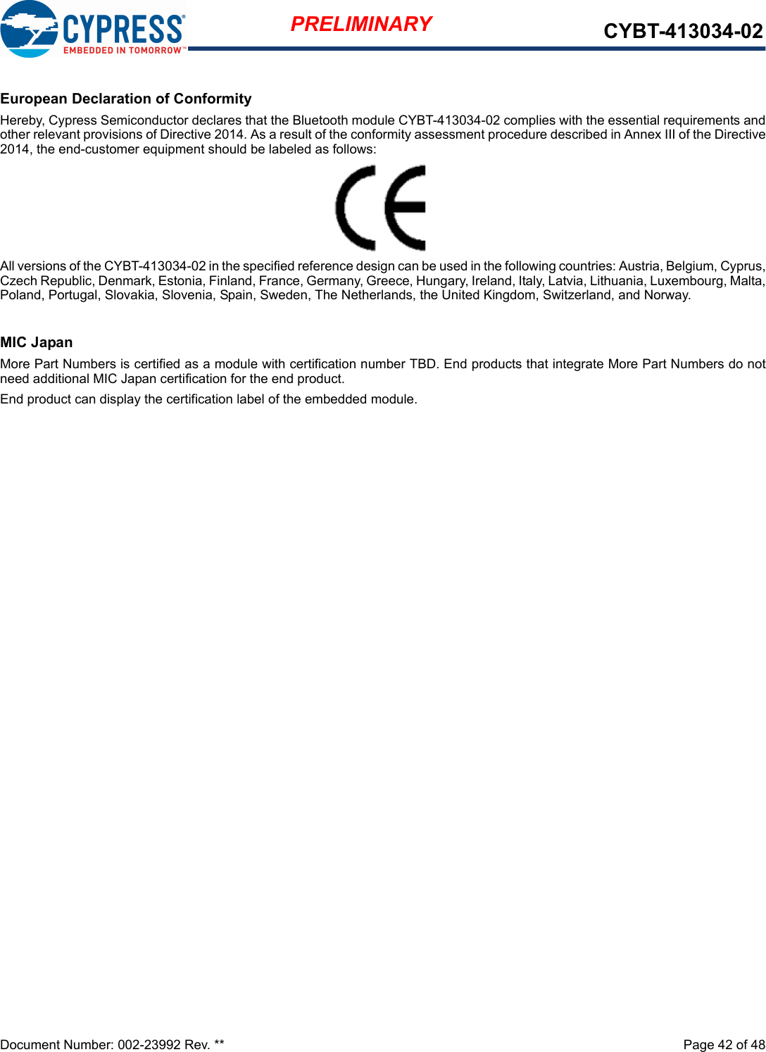
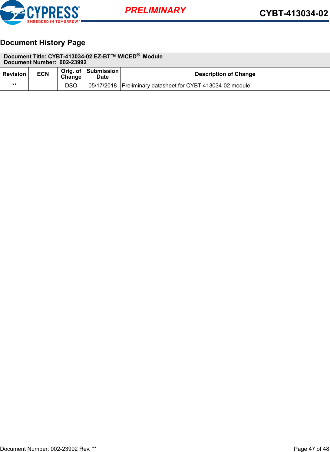
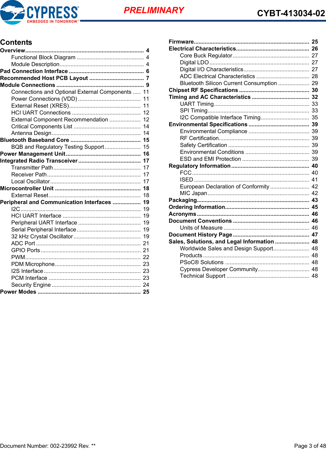
![Document Number: 002-23992 Rev. ** Page 39 of 48PRELIMINARY CYBT-413034-02Environmental SpecificationsEnvironmental ComplianceThis Cypress BLE module is produced in compliance with the Restriction of Hazardous Substances (RoHS) and Halogen-Free (HF)directives. The Cypress module and components used to produce this module are RoHS and HF compliant.RF CertificationThe CYBT-413034-02 module is certified under the following RF certification standards:nFCC: TBDnISED: TBDnMIC: TBDnCESafety CertificationThe CYBT-413034-02 module complies with the following safety regulations:nUnderwriters Laboratories, Inc. (UL): Filing E331901nCSAnTUVEnvironmental ConditionsTable 28 describes the operating and storage conditions for the Cypress BLE module.ESD and EMI ProtectionExposed components require special attention to ESD and electromagnetic interference (EMI).A grounded conductive layer inside the device enclosure is suggested for EMI and ESD performance. Any openings in the enclosurenear the module should be surrounded by a grounded conductive layer to provide ESD protection and a low-impedance path to ground. Device Handling: Proper ESD protocol must be followed in manufacturing to ensure component reliability.Table 28. Environmental Conditions for CYBT-413034-02Description Minimum Specification Maximum SpecificationOperating temperature −30 °C 85 °COperating humidity (relative, non-condensation) 5% 85%Thermal ramp rate – 10 °C/minuteStorage temperature –40 °C 85 °CStorage temperature and humidity – 85 °C at 85%ESD: Module integrated into system Components[4] –15 kV Air2.0 kV ContactNote4. This does not apply to the RF pins (ANT).](https://usermanual.wiki/Cypress-Semiconductor/3034/User-Guide-3884229-Page-39.png)