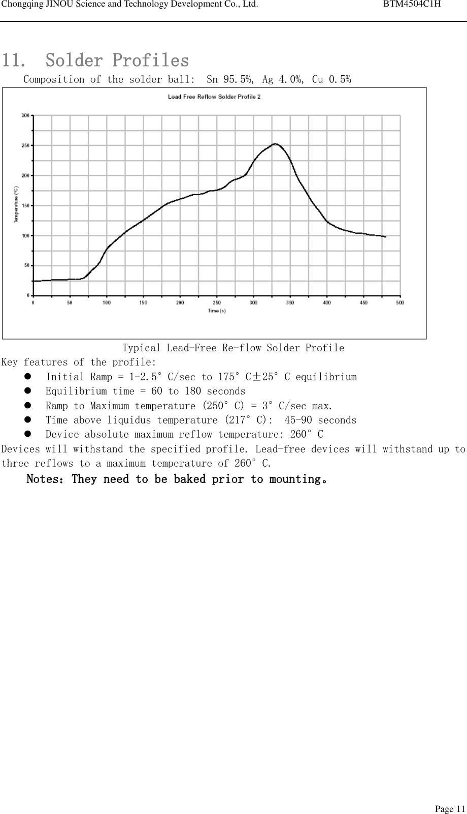
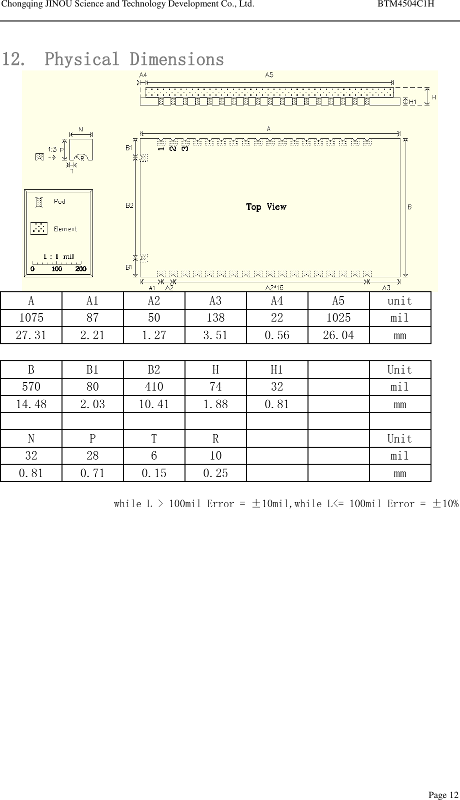
Chongqing Jinou Science and Technology Development BTM4504C1H Class1 Bluetooth Module User Manual
Chongqing Jinou Science & Technology Development Co., Ltd. Class1 Bluetooth Module
UserManual.wiki
>
Chongqing Jinou Science and Technology Development
>
BTM4504C1H User Manual
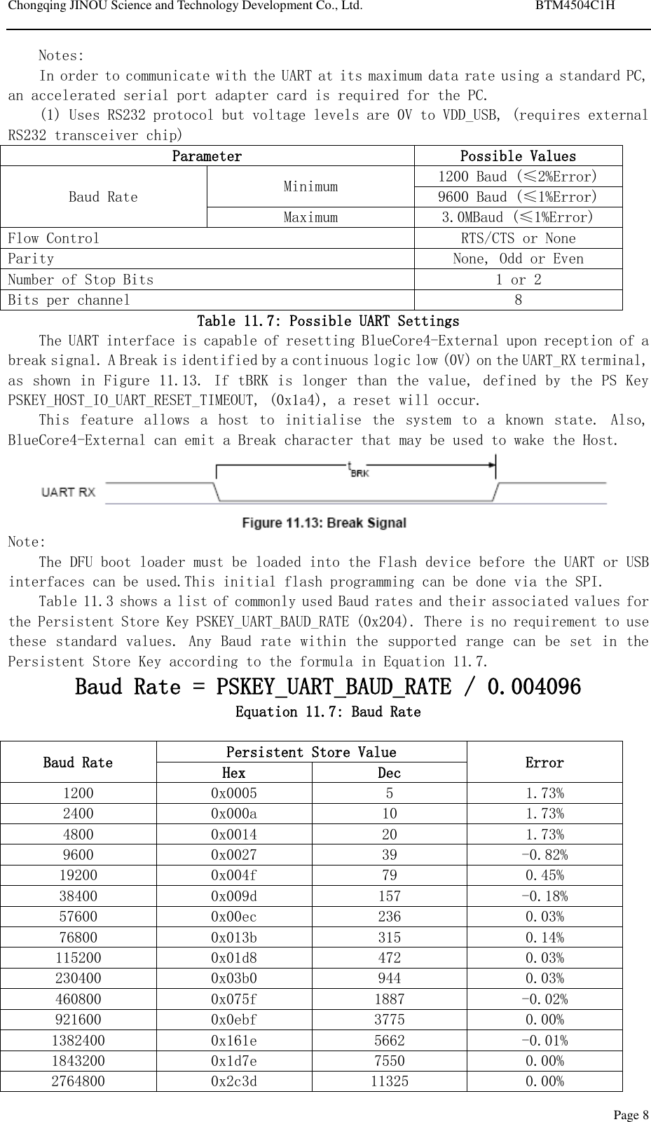
User Manual
Navigation menu
Upload a User Manual
Namespaces
Wiki Guide
HTML
PDF
Info
Views
User Manual
Discussion / Help
Navigation
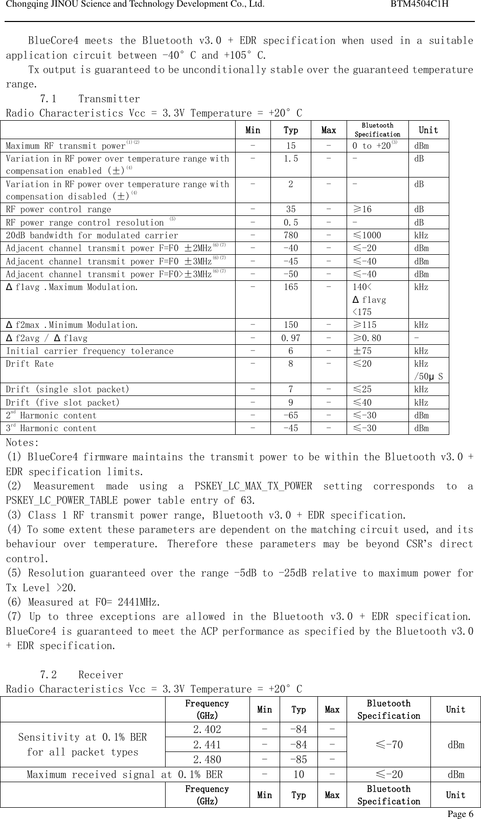
![Chongqing JINOU Science and Technology Development Co., Ltd. BTM4504C1H Page 9 Table 11.8: Standard Baud Rates 8.1 UART Bypass Figure 11.14: UART Bypass Architecture 8.2 UART Configuration While RESET is Active The UART interface for BlueCore4-External while the chip is being held in reset is tri-state. This will allow the user to daisy chain devices onto the physical UART bus. The constraint on this method is that any devices connected to this bus must tri-state when BlueCore4-External reset is de-asserted and the firmware begins to run. 8.3 UART Bypass Mode Alternatively, for devices that do not tri-state the UART bus, the UART bypass mode on BlueCore4-External can be used. The default state of BlueCore4-External after reset is de-asserted, this is for the host UART bus to be connected to the BlueCore4-External UART, thereby allowing communication to BlueCore4-External via the UART. In order to apply the UART bypass mode, a BCCMD command will be issued to BlueCore4-External upon this, it will switch the bypass to PIO[7:4] as shown in Figure 11.14. Once the bypass mode has been invoked, BlueCore4-External will enter the deep sleep state indefinitely. In order to re-establish communication with BlueCore4-External, the chip must be reset so that the default configuration takes affect. It is important for the host to ensure a clean Bluetooth disconnection of any active links before the bypass mode is invoked. Therefore it is not possible to have active Bluetooth links while operating the bypass mode. 8.4 Current Consumption in UART Bypass Mode The current consumption for a device in UART Bypass Mode is equal to the values quoted for a device in standby mode. 9. I/O Parallel PortsFifteen lines of programmable bi-directional input/outputs (I/O) are provided.PIO[11:8] and PIO[3:0] are powered from Vcc. PIO[7:4] are powered from Vcc. AIO [2:0] are powered from Vref. PIO lines can be configured through software to have either weak or strong pull-ups or pull-downs. All PIO lines are configured as inputs with weak pull-downs at reset. PIO[0] and PIO[1] are normally dedicated to RXEN and TXEN respectively, but they are available for general use. Any of the PIO lines can be configured as interrupt request lines or as wake-up lines from sleep modes. PIO[6] or PIO [2] can be configured as a request line for an external clock source. This is useful when the clock to BlueCore4-External is provided from a](https://usermanual.wiki/Chongqing-Jinou-Science-and-Technology-Development/BTM4504C1H/User-Guide-3947404-Page-10.png)
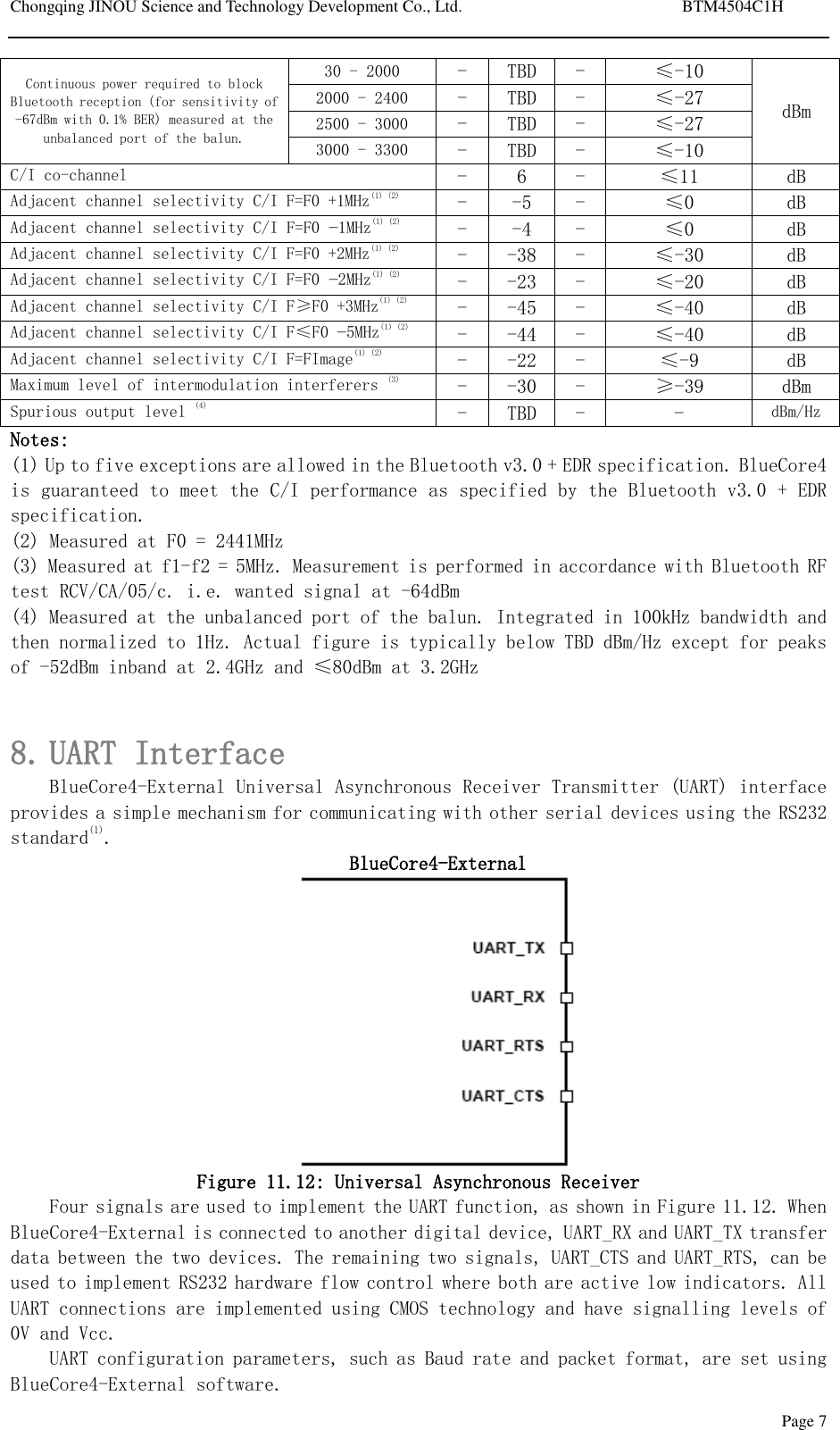
![Chongqing JINOU Science and Technology Development Co., Ltd. BTM4504C1H Page 10 system application specific integrated circuit (ASIC). BlueCore4-External has three general purpose analogue interface pins, AIO[0], AIO[1] and AIO[2]. These are used to access internal circuitry and control signals. One pin is allocated to decoupling for the on-chip band gap reference voltage, the other three may be configured to provide additional functionality. Auxiliary functions available via these pins include an 8-bit ADC and an 8-bit DAC. Typically the ADC is used for battery voltage measurement. Signals selectable at these pins include the band gap reference voltage and a variety of clock signals; 48, 24, 16, 8MHz and the XTAL clock frequency. When used with analogue signals the voltage range is constrained by the analogue supply voltage (1.8V). When configured to drive out digital level signals (clocks) generated from within the analogue part of the device, the output voltage level is determined by Vref (1.8V). Important Note: CSR cannot guarantee that terminal functions PIOs remain the same. Please refer to the software release note for the implementation of these PIO lines, as they are firmware build specific. 10. RESETBBlueCore4 Module may be reset from several sources: power on reset, a UART break character or via a software configured watchdog timer. The power on reset occurs when the VDD_CORE supply falls below typically 1.5V and is released when VDD_CORE rises above typically 1.6V. At reset the digital I/O pins are set to inputs for bi-directional pins and outputs are tri-stated. The PIOs have weak pull-downs. Following a reset, BlueCore4-External assumes the maximum XTAL_IN frequency, which ensures that the internal clocks run at a safe (low) frequency until BlueCore4-External is configured for the actual XTAL_IN frequency. If no clock is present at XTAL_IN, the oscillator in BlueCore4-External free runs, again at a safe frequency. 10.1 Pin States on Reset Table 11.15 shows the pin states of BlueCore4-External on reset. Pin Name State: BlueCore4-External PIO[6:2] Input with weak pull-down UART_TX Output tri-stated with weak pull-up UART_RX Input with weak pull-down UART_RTS Output tri-stated with weak pull-up UART_CTS Input with weak pull-down SPI_CSB Input with weak pull-up SPI_CLK Input with weak pull-down SPI_MOSI Input with weak pull-down SPI_MISO Output tri-stated with weak pull-down AIO[1] Output, driving low Table 11.15: Pin States of BlueCore4-External on Reset 10.2 Status after Reset The chip status after a reset is as follows: Warm Reset: Baud rate and RAM data remain availableCold Reset(1): Baud rate and RAM data not availableNote: (1) Cold Reset constitutes one of the following: Power cycleSystem reset (firmware fault code)](https://usermanual.wiki/Chongqing-Jinou-Science-and-Technology-Development/BTM4504C1H/User-Guide-3947404-Page-11.png)