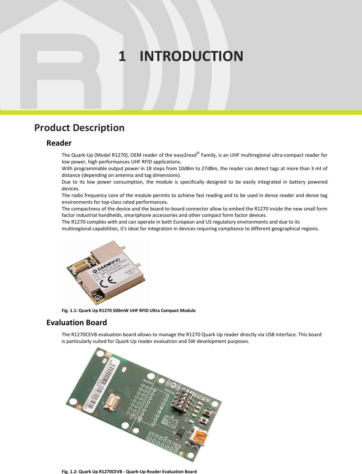
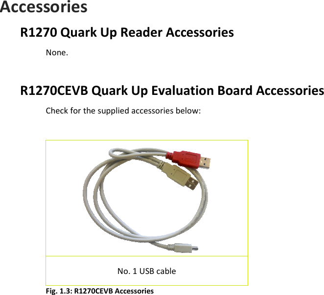
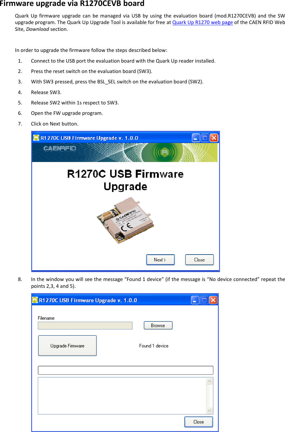
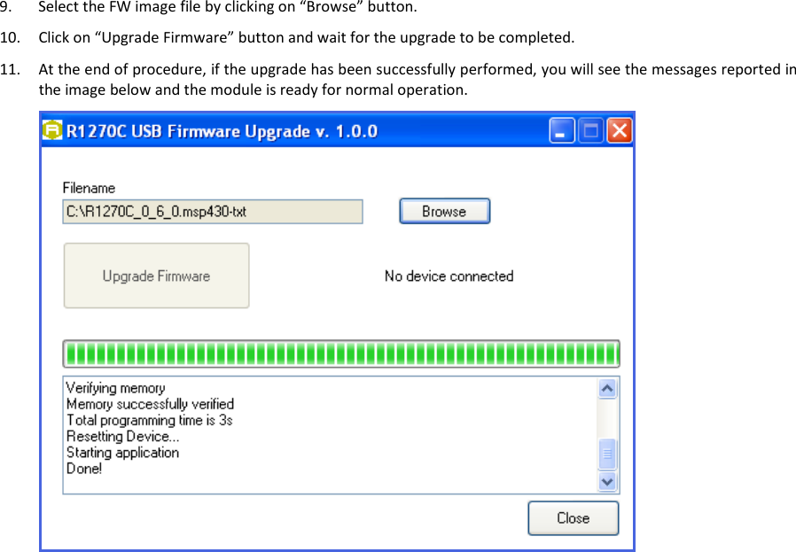
CAEN RFID srl CAENRFID015 UHF RFID Ultra Compact Reader User Manual Technical Information Manual
CAEN RFID srl UHF RFID Ultra Compact Reader Technical Information Manual
Contents
- 1. users manual
- 2. technical information manual
- 3. quark up technical information manual
- 4. Technical Information Manual
Technical Information Manual
![Scope of Manual The goal of this manual is to provide the basic information to work with the Quark Up R1270 500mW UHF RFID Ultra Compact Module. Change Document Record Date Revision Changes Pages 12 Oct 2016 01 First release - 18 May 2018 02 Modified REGULATORY COMPLIANCE chapter 29 Modified Technical Specifications Table 10 Added USB Communication Setup 27 Modified R1270 Quark up photo 1-6 4 June 2018 02.1 Added information for FCC Class II Permissive Change: - Dual antenna configuration - Addition of 7R1251IUNFAA to approved antenna list 18,29 Reference Document [RD1] EPCglobal: EPC Radio-Frequency Identity Protocols Class-1 Generation-2 UHF RFID Protocol for Communications at 860 MHz – 960 MHz, Version 2.0.1 (April, 2015). CAEN RFID srl Via Vetraia, 11 55049 Viareggio (LU) - ITALY Tel. +39.0584.388.398 Fax +39.0584.388.959 info@caenrfid.com www.caenrfid.com © CAEN RFID srl – 2018 Disclaimer No part of this manual may be reproduced in any form or by any means, electronic, mechanical, recording, or otherwise, without the prior written permission of CAEN RFID. The information contained herein has been carefully checked and is believed to be accurate; however, no responsibility is assumed for inaccuracies. CAEN RFID reserves the right to modify its products specifications without giving any notice; for up to date information please visit www.caenrfid.com. Visit the Quark Up R1270 web page, you will find the latest revision of data sheets, manuals, certifications, technical drawings, software and firmware. All you need to start using your reader in a few clicks!](https://usermanual.wiki/CAEN-RFID-srl/CAENRFID015.Technical-Information-Manual/User-Guide-3908907-Page-2.png)
![QUARK UP R1270 - Quark Up Technical Information Manual 10 2 QUARK UP R1270 Technical Specifications Table Frequency Band 865.600÷867.600 MHz (ETSI EN 302 208 v3.1.1) 902÷928 MHz (FCC part 15.247) RF Power Programmable in 18 levels (1dB step) from 10dBm to 27dBm (from 10mW to 500mW) conducted Output Power Accuracy +/- 1dB Antenna VSWR Requirement 2:1 or better for optimum performances Antenna Connector Nr. 1 U.FL type Frequency Tolerance ±10 ppm over the entire temperature range Number of Channels 4 channels (compliant to ETSI EN 302 208 v3.1.1) 50 hopping channels (compliant to FCC part 15.247). Standard Compliance EPC C1G2 [RD1]/ISO 18000-63 Digital I/O 4 I/O lines (3.3V level; Iout=3mA max) Connectivity USB interface: One USB 2.0 Full Speed (12Mbit/s) device port UART Serial Port: Baudrate: up to 115200 Databits: 8 Stopbits: 1 Parity: none Flow control: none 3.3 V I/O Voltage Level DC Power 5.0 VDC+/-5% Power Consumption 2.7W @ RF out = 27dBm 1.6W @ RF out = 23dBm 0.15W in idle mode Operating Temperature -10 °C to +55 °C Dimensions (W)25 x (L)25 x (H)6 mm3 (1.0 x 1.0 x 0.2 inch3) Weight 5 g Tab. 2.1: Quark Up R1270 Technical Specifications Warning: The RF settings must match the country/region of operating to comply with local laws and regulations. It is not allowed the use in different countries/regions from the one in which the device has been sold. Y](https://usermanual.wiki/CAEN-RFID-srl/CAENRFID015.Technical-Information-Manual/User-Guide-3908907-Page-10.png)
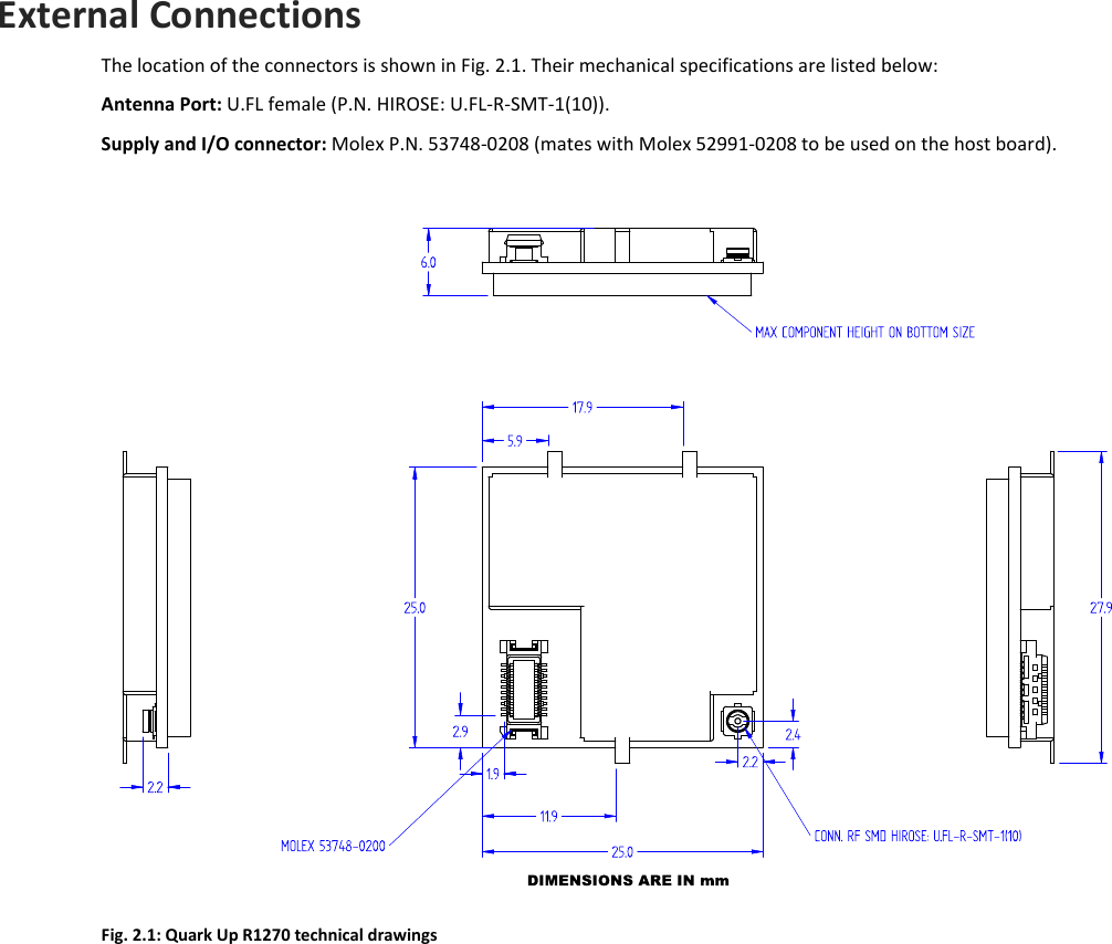
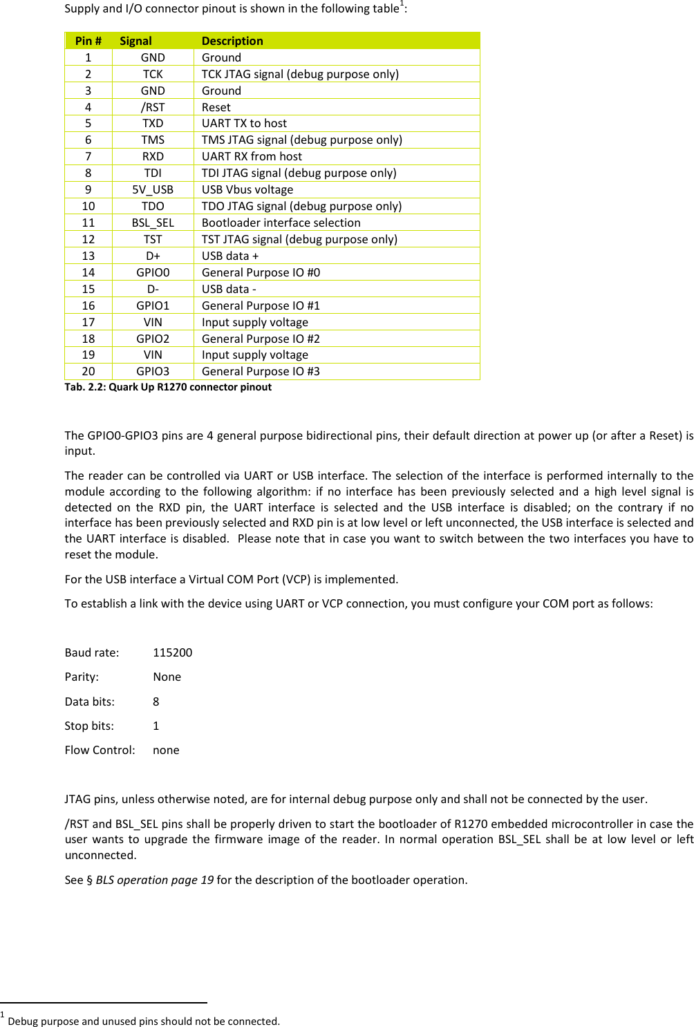
![QUARK UP R1270 - Quark Up Technical Information Manual 13 R1270 supply and I/O connector electrical characteristics2 Pin name Pin No. Parameter Min Type Max Unit GND 1,3 TCK 2 VIL -0.3 0.75 V VIH 1.5 3.6 V Input current 10 μA /RESET 4 VIL -0.3 0.6 V VIH 1.65 3.6 V Internal pull-up resistance 47 kΩ Pulse width 10 μs TXD 5 VOL 0 0.55 V VOH 2.5 3.5 V Output current 3.0 mA TMS 6 VIL -0.3 0.75 V VIH 1.5 3.6 V Input current 10 μA RXD 7 VIL -0.3 0.75 V VIH 1.5 3.6 V Input current 10 μA TDI 8 VIL -0.3 0.75 V VIH 1.5 3.6 V Input current 10 μA 5V_USB 9 Input DC voltage 4.75 5.00 5.25 V Input current 20 mA TDO 10 VOL 0 0.55 V VOH 2.5 3.5 V Output current 3.0 μA BSL_SEL 11 VIL -0.3 1.0 V VIH 2.2 3.6 V Internal pull-down resistance 10 kΩ TST 12 VIL -0.3 0.75 V VIH 1.5 3.6 V Internal pull-down resistance 45 kΩ D+,D- 13,15 VOL 0 0.3 V VOH 2.8 3.6 V Impedance 28 44 Ω GPIO[0:3] 14, 16, 18, 20 VOL 0 0.55 V VOH 2.5 3.5 V Output current 3.0 mA VIL -0.3 0.75 V VIH 1.5 3.6 V Input current 10 μA 2 Exceeding maximum values reported in the table may cause permanent damage to the model.](https://usermanual.wiki/CAEN-RFID-srl/CAENRFID015.Technical-Information-Manual/User-Guide-3908907-Page-13.png)
![QUARK UP R1270CEVB - Quark Up Technical Information Manual 23 3 QUARK UP R1270CEVB Technical Specifications Table Switch SW1= GPIO SW2= BSL_SEL SW3= RESET USB Port Mini USB Type A plug connector Bus powered USB 2.0 device Must be connected to two High-power Port (500 mA @ VBUS) with a dual USB cable. It appears as USB serial port Virtual Com Port (VCP) 5 drivers for Windows XP/Vista/Seven (7) Baudrate: 115200 Databits: 8 Stopbits: 1 Parity: none Flow control: none User Interface Red LED: Power Green LED: GPIO[0..3]. Dimensions (W)38.0 x (L)76.0 x (H)12.0 mm3 (1.5 x 3.0 x 0.5 inch3) Electrical Power DC Voltage 5V +/-5% Max 800 mA6 Operating Temperature -10 °C to +55 °C Tab. 3.1: R1270CEVB - Quark-Up Reader Evaluation Board Warning: The RF settings must match the country/region of operating to comply with local laws and regulations. The usage of the reader in different countries/regions from the one in which the device has been sold is not allowed. 5 You can download VCP drivers for Windows based systems from the CAEN RFID Web Site at Quark Up R1270 page. 6 With Quark Up reader operating. Y](https://usermanual.wiki/CAEN-RFID-srl/CAENRFID015.Technical-Information-Manual/User-Guide-3908907-Page-23.png)