CAEN RFID srl CAENRFID010 Low Power OEM UHF Compact RFID Reader User Manual CAENRFIDLibrary
CAEN RFID srl Low Power OEM UHF Compact RFID Reader CAENRFIDLibrary
Contents
- 1. Users Manual I
- 2. Users Manual II
- 3. Users Manual III
- 4. Users Manual IV
- 5. User Manual
Users Manual III
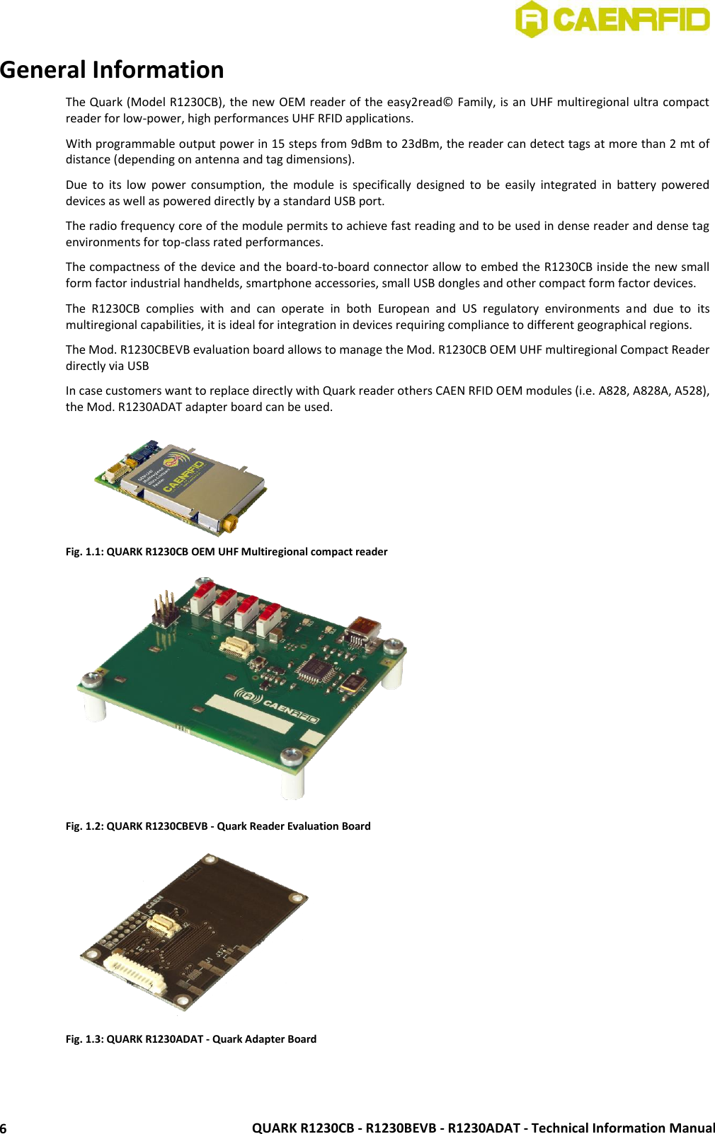
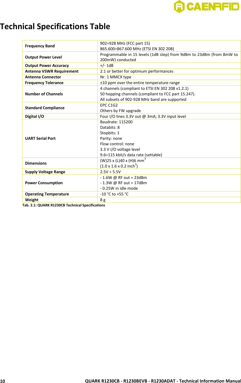
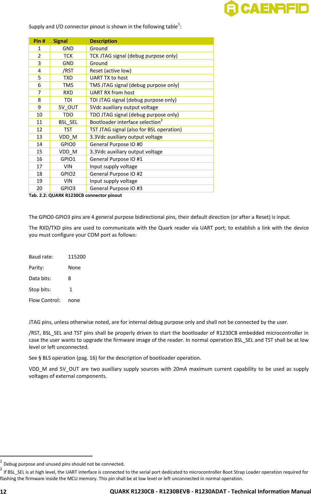
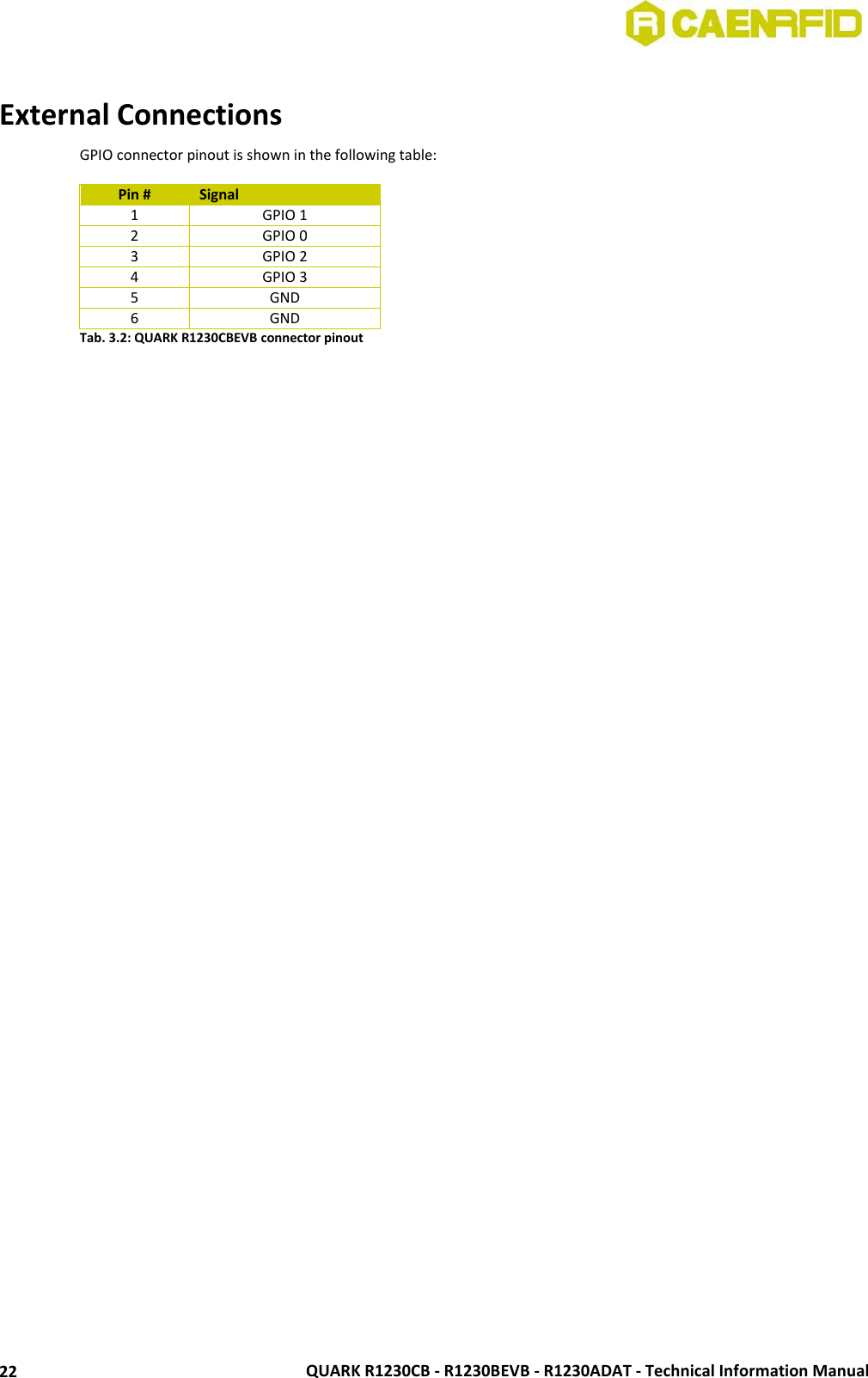
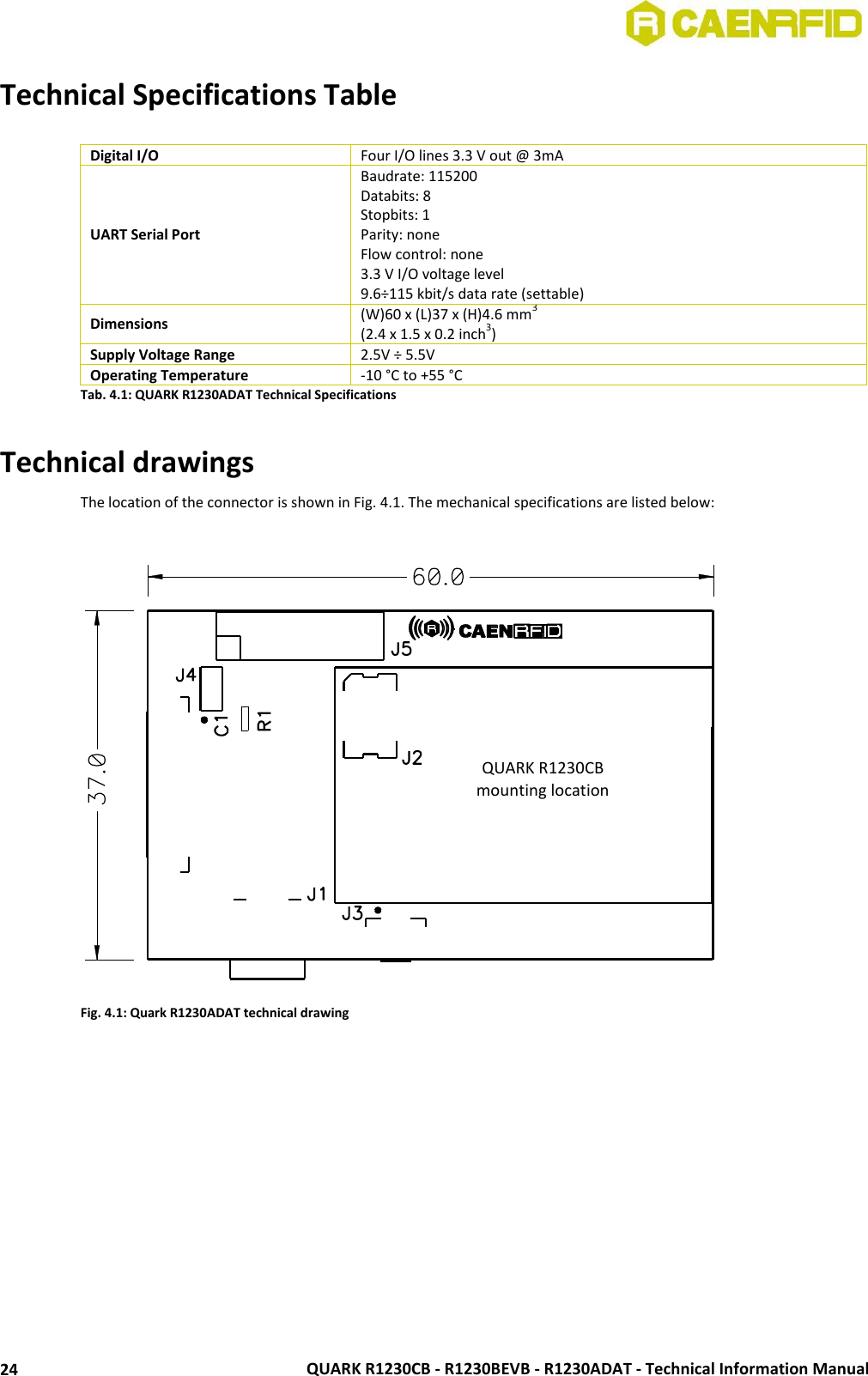
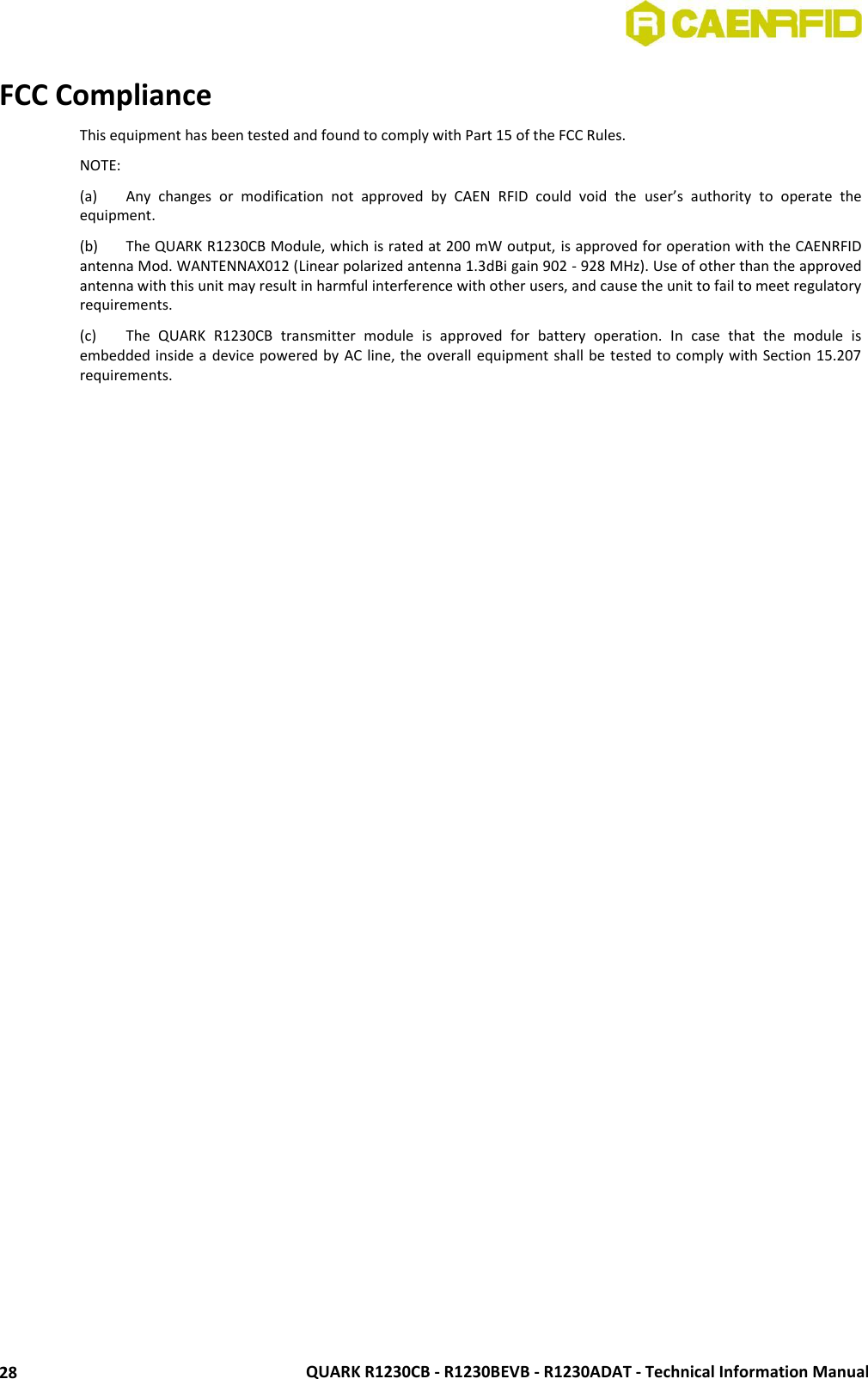
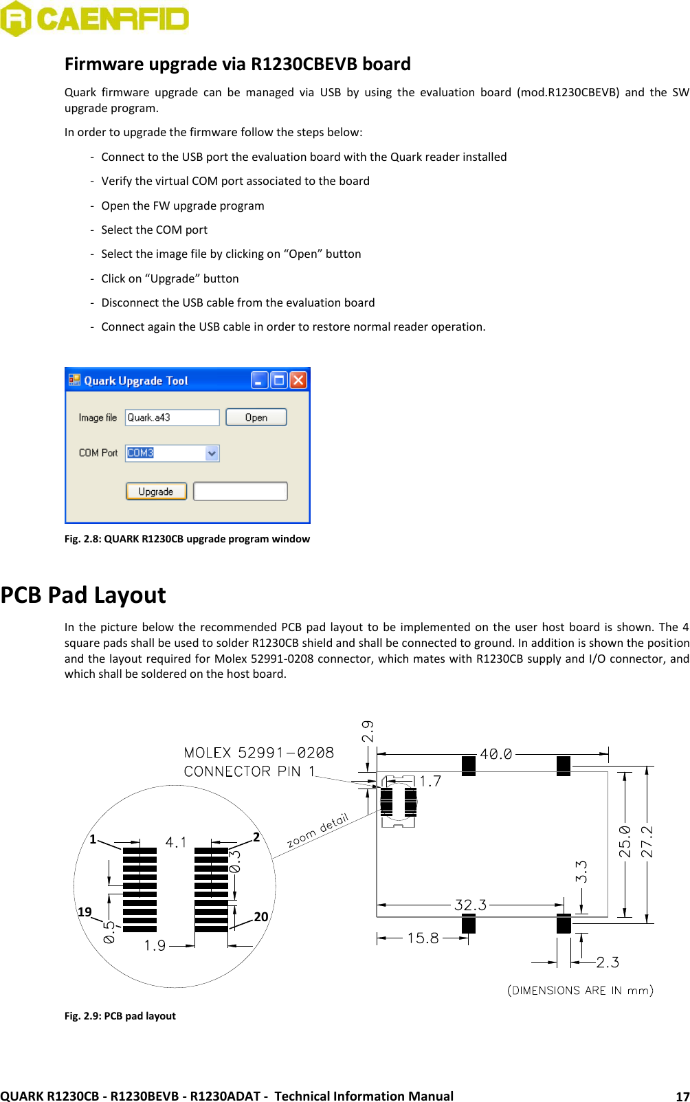
![QUARK R1230CB - R1230BEVB - R1230ADAT - Technical Information Manual 13 R1230CB supply and I/O connector electrical characteristics3 Pin name Pin No. Parameter Min Type Max Unit GND 1,3 TCK 2 VIL -0.3 0.75 V VIH 1.5 3.6 V Input current 10 μA /RESET 4 VIL -0.3 0.6 V VIH 1.65 3.6 V Internal pull-up resistance 47 kΩ Pulse width 10 μs TXD 5 VOL 0 0.55 V VOH 2.5 3.5 V Output current 3.0 mA TMS 6 VIL -0.3 0.75 V VIH 1.5 3.6 V Input current 10 μA RXD 7 VIL -0.3 0.75 V VIH 1.5 3.6 V Input current 10 μA TDI 8 VIL -0.3 0.75 V VIH 1.5 3.6 V Input current 10 μA 5V_OUT 9 Output DC voltage 4.75 5.00 5.25 V Output current 20 mA TDO 10 VOL 0 0.55 V VOH 2.5 3.5 V Output current 3.0 μA BSL_SEL 11 VIL -0.3 1.0 V VIH 2.2 3.6 V Internal pull-down resistance 10 kΩ TST 12 VIL -0.3 0.75 V VIH 1.5 3.6 V Internal pull-down resistance 45 kΩ VDD_M 13,15 Output DC voltage 3.1 3.3 3.5 V Output current 20 mA GPIO[0:3] 14, 16, 18, 20 VOL 0 0.55 V VOH 2.5 3.5 V Output current 3.0 mA VIL -0.3 0.75 V VIH 1.5 3.6 V Input current 10 μA VIN4 17,19 Input supply voltage 2.5 5.5 V Supply current @ Vin = 2.5V 0.68 A Supply current @ Vin = 3.7V 0.42 A Supply current @ Vin = 5.0V 0.30 A Tab. 2.3: QUARK R1230CB supply and I/O connector electrical characteristics 3 Exceeding maximum values reported in the table may cause permanent damage to the model. 4 External 100uF bypass capacitor between Vin and GND is recommended for proper operation.](https://usermanual.wiki/CAEN-RFID-srl/CAENRFID010.Users-Manual-III/User-Guide-1405618-Page-13.png)
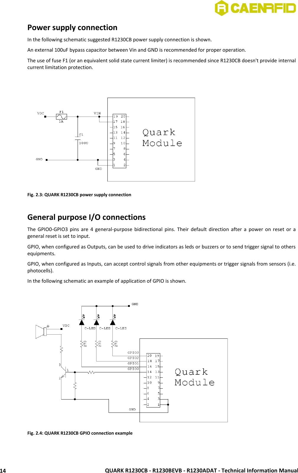
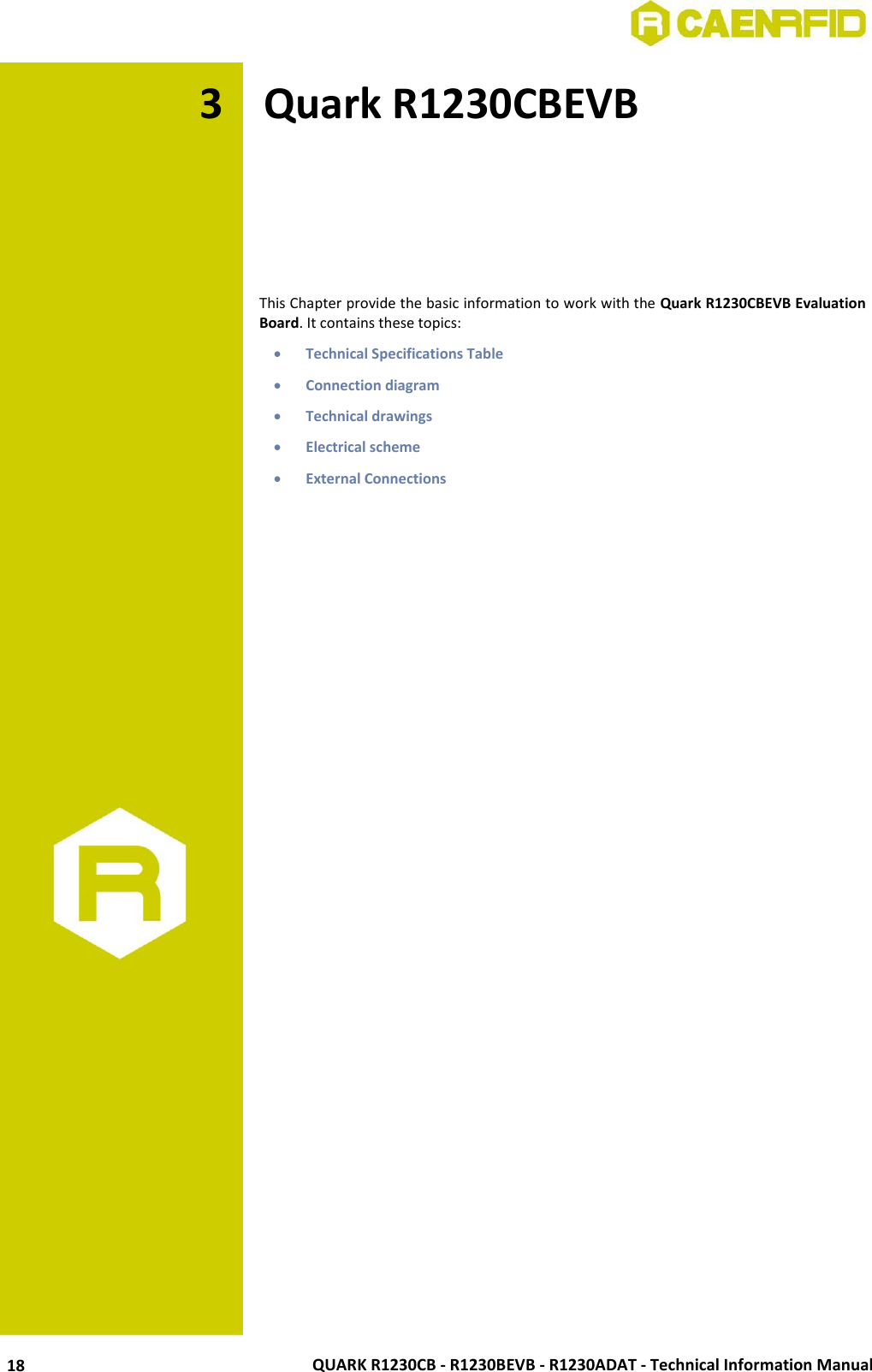
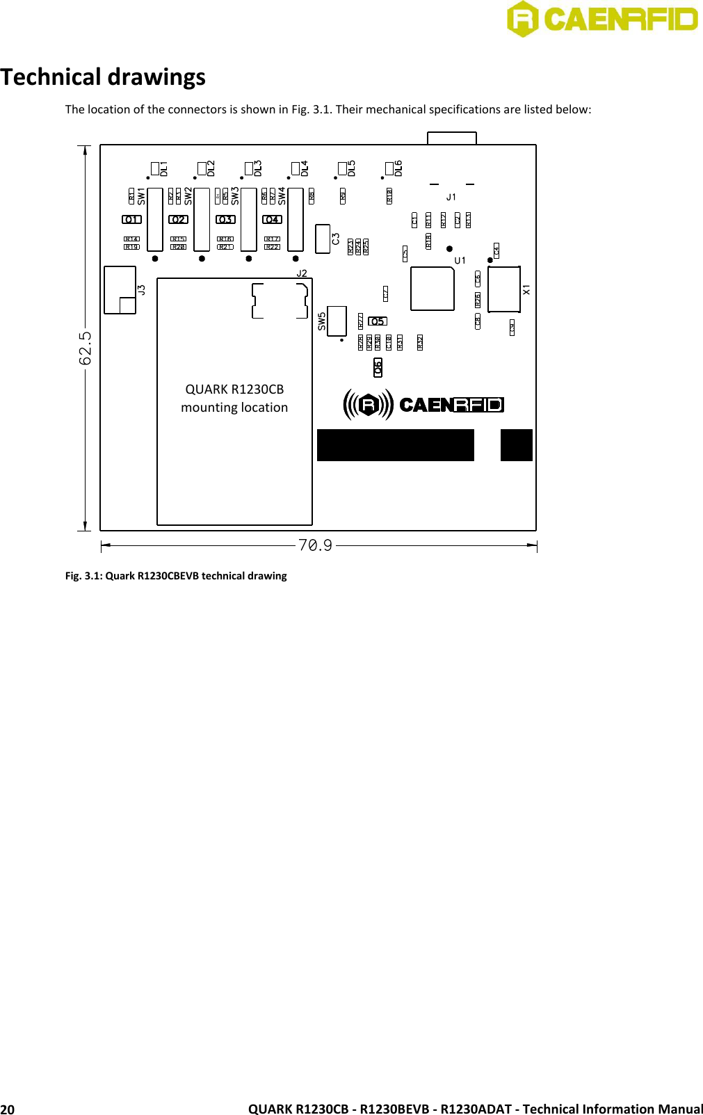
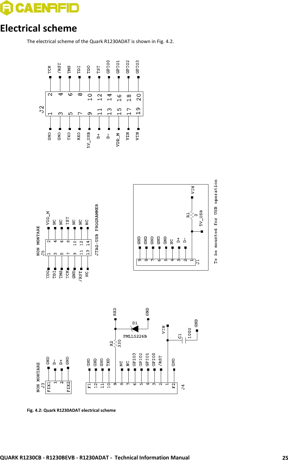
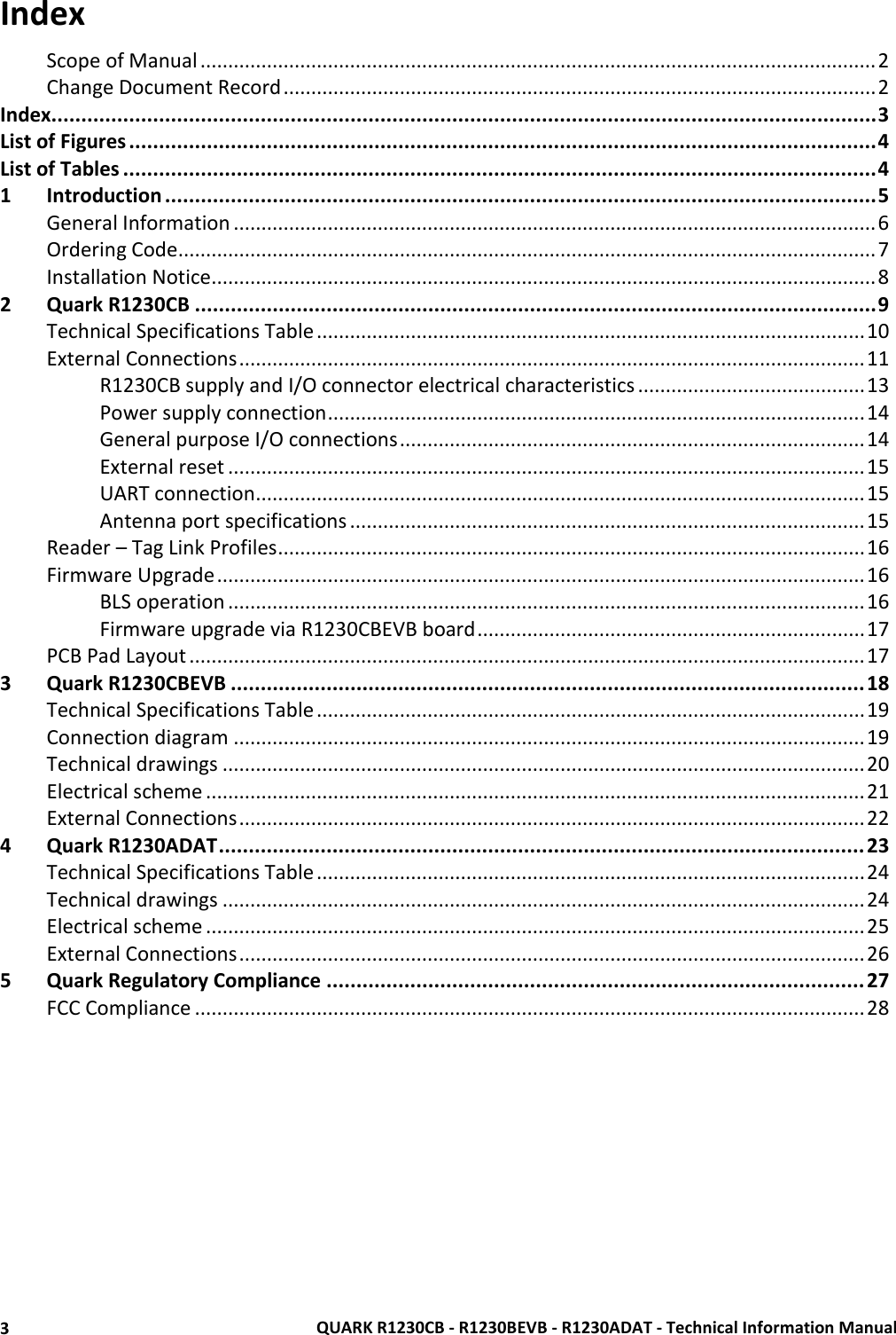
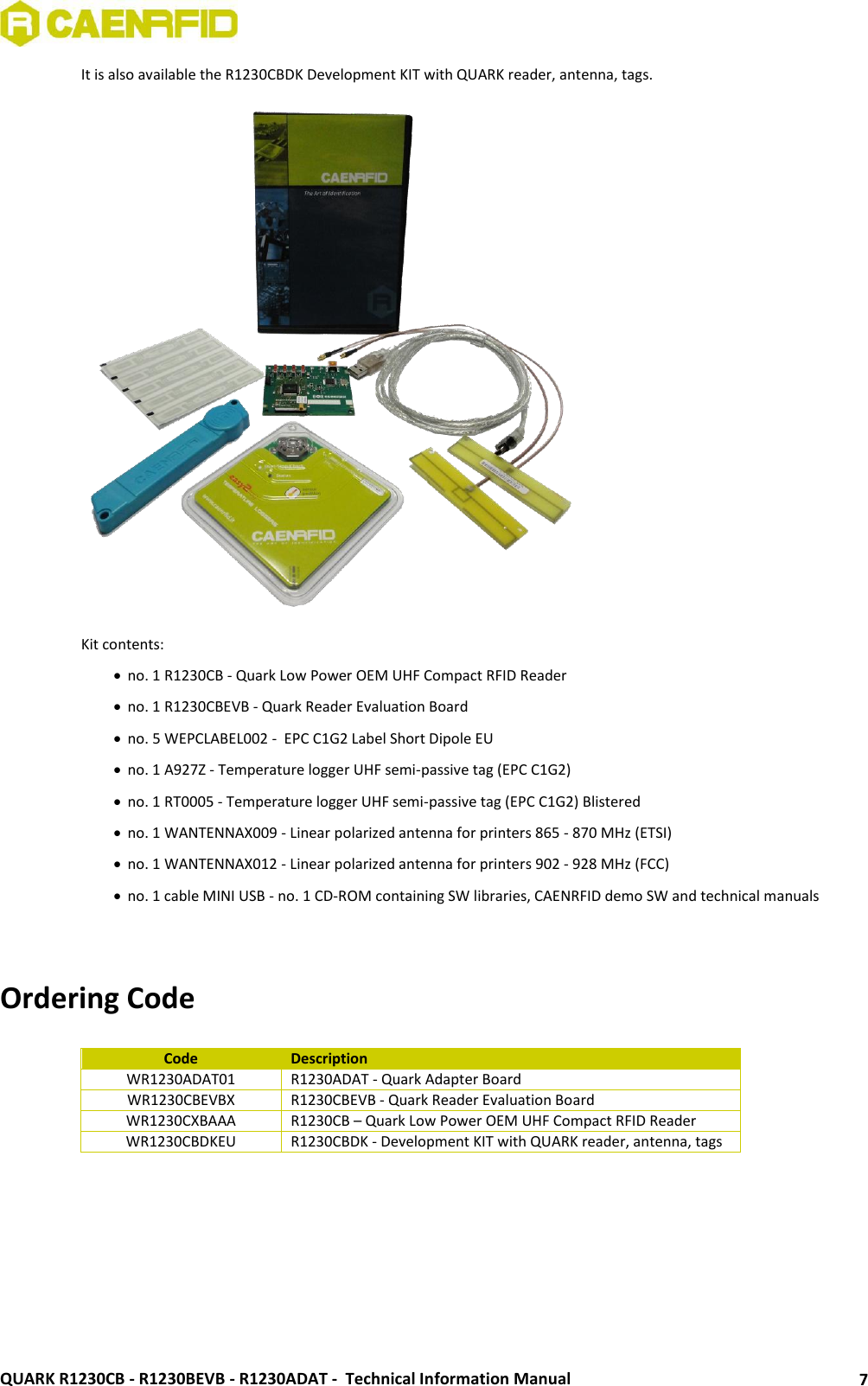
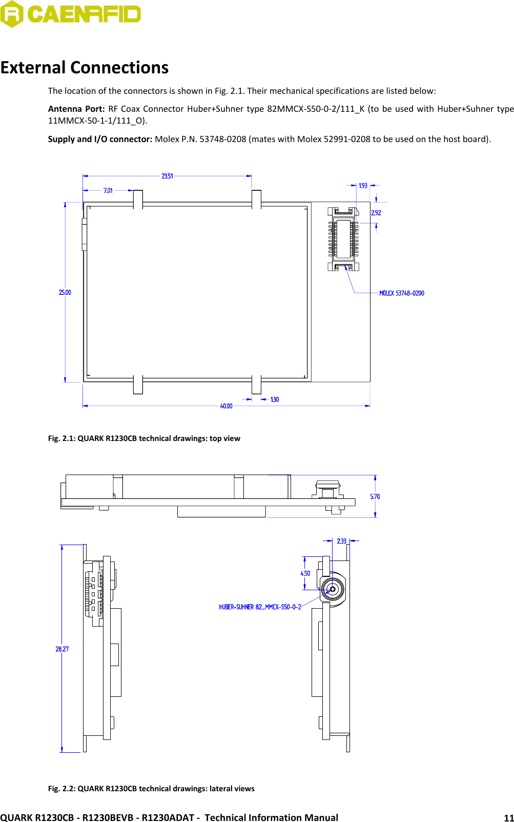
![QUARK R1230CB - R1230BEVB - R1230ADAT - Technical Information Manual 19 Technical Specifications Table Switch SW1= RESET SW2...SW5=GPIO USB Port USB Type A plug connector Bus powered USB 2.0 device Must be connected to Hight-power Port (500 mA @ VBUS) It appears as USB serial port Virtual Com Port (VCP) drivers for Windows XP/Vista/Seven (7), Windows CE 4.2, Linux 2.40 and greater Baudrate: 115200 Databits: 8 Stopbits: 1 Parity: none Flow control: none User Interface Red LED: Power Yellow LED: USB communication activity Green LED: GPIO[0..3]. Dimensions (W)70.9 x (L)62.5 x (H)11.6 mm3 (2.8 x 2.5 x 0.5 inch3) Electrical Power DC Voltage 5V +/-5% Max 400 mA5 Operating Temperature -10 °C to +55 °C Tab. 3.1: QUARK R1230CBEVB Technical Specifications Connection diagram The following block diagram shows how to connect the Mod. R1230CB with the PC host via the Mod. R1230CBEVB evaluation board. 5 With Quark reader operating. Antenna USB R1230CBEVB Molex Connector R1230CB OEM UHF Multiregional Ultra Compact Reader to host](https://usermanual.wiki/CAEN-RFID-srl/CAENRFID010.Users-Manual-III/User-Guide-1405618-Page-19.png)