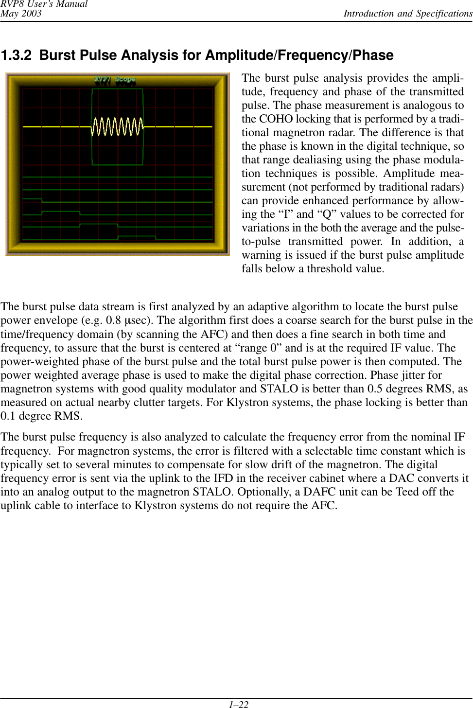
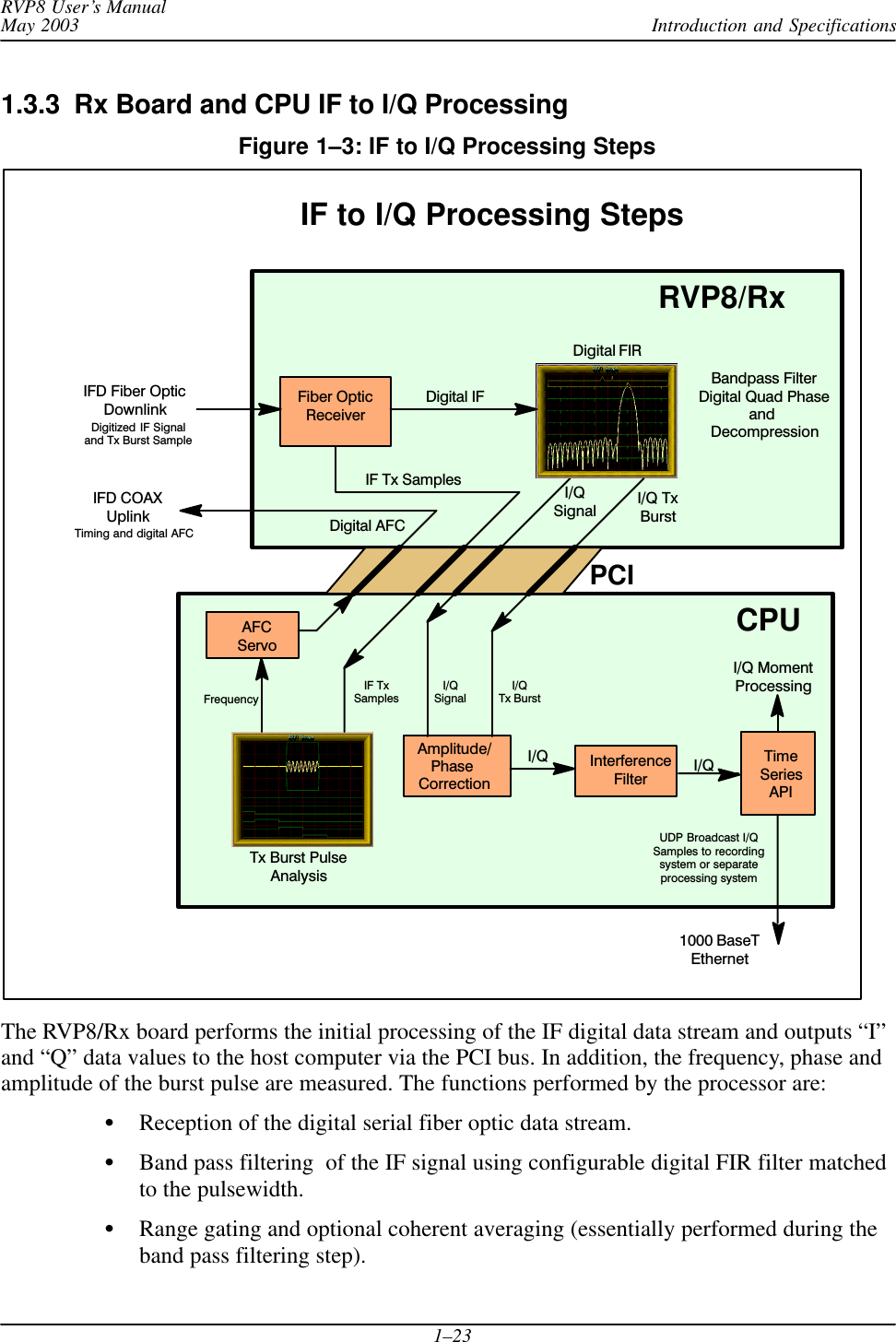
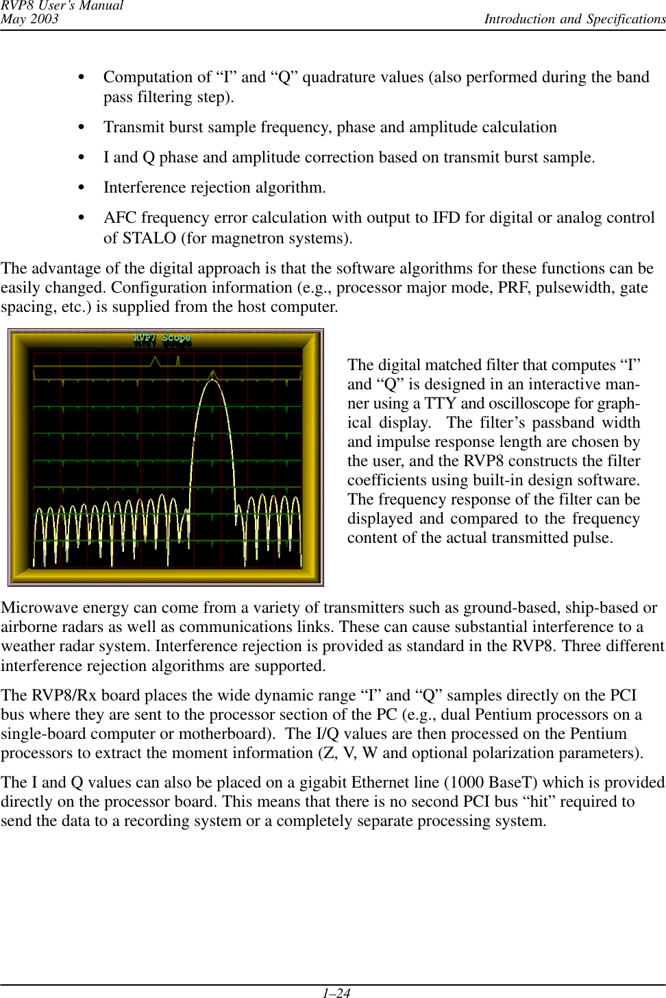
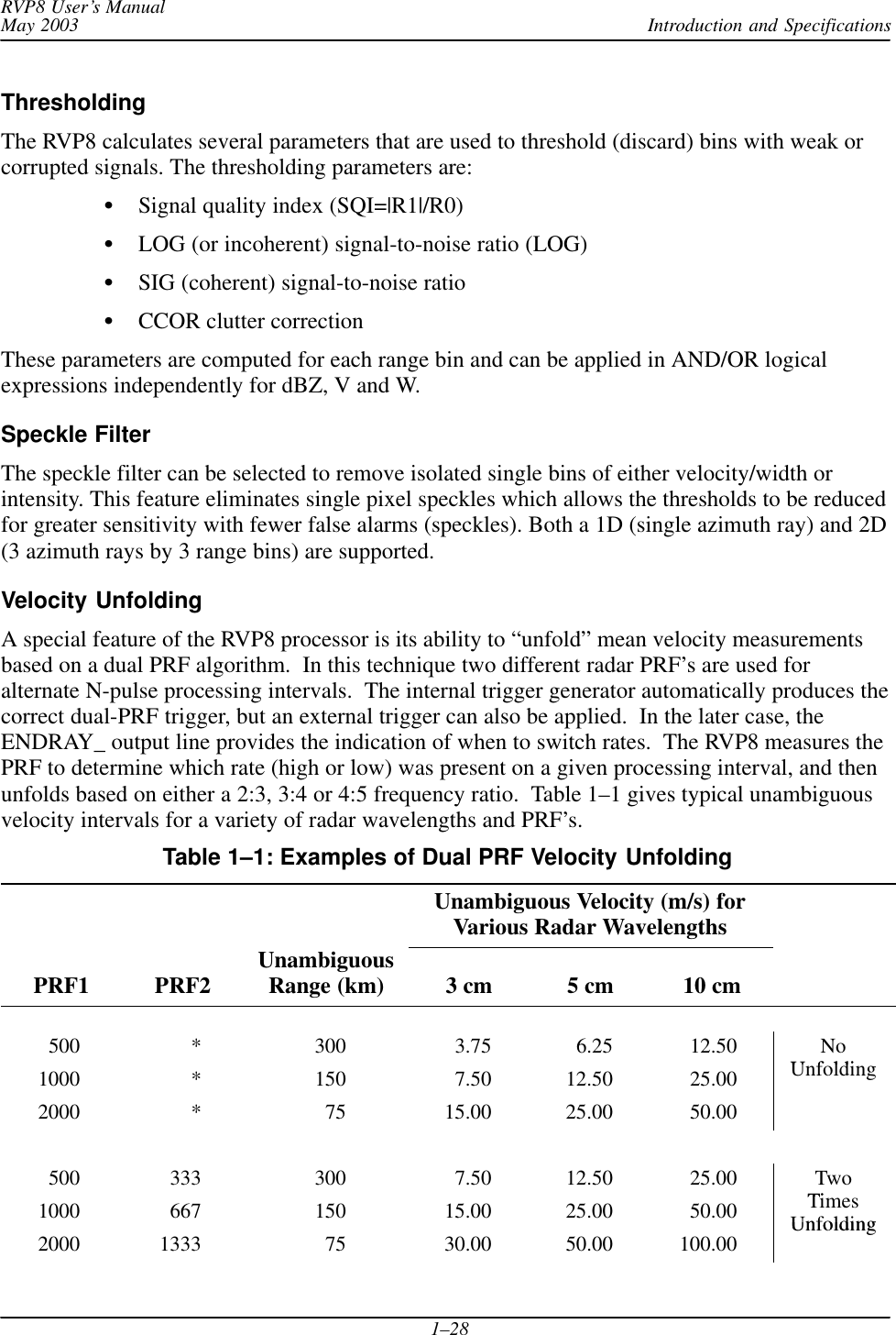
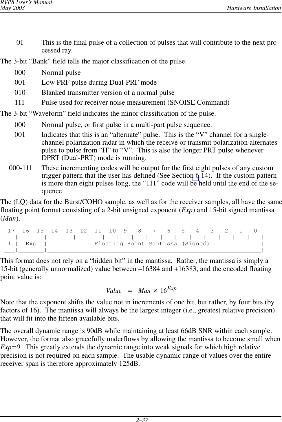
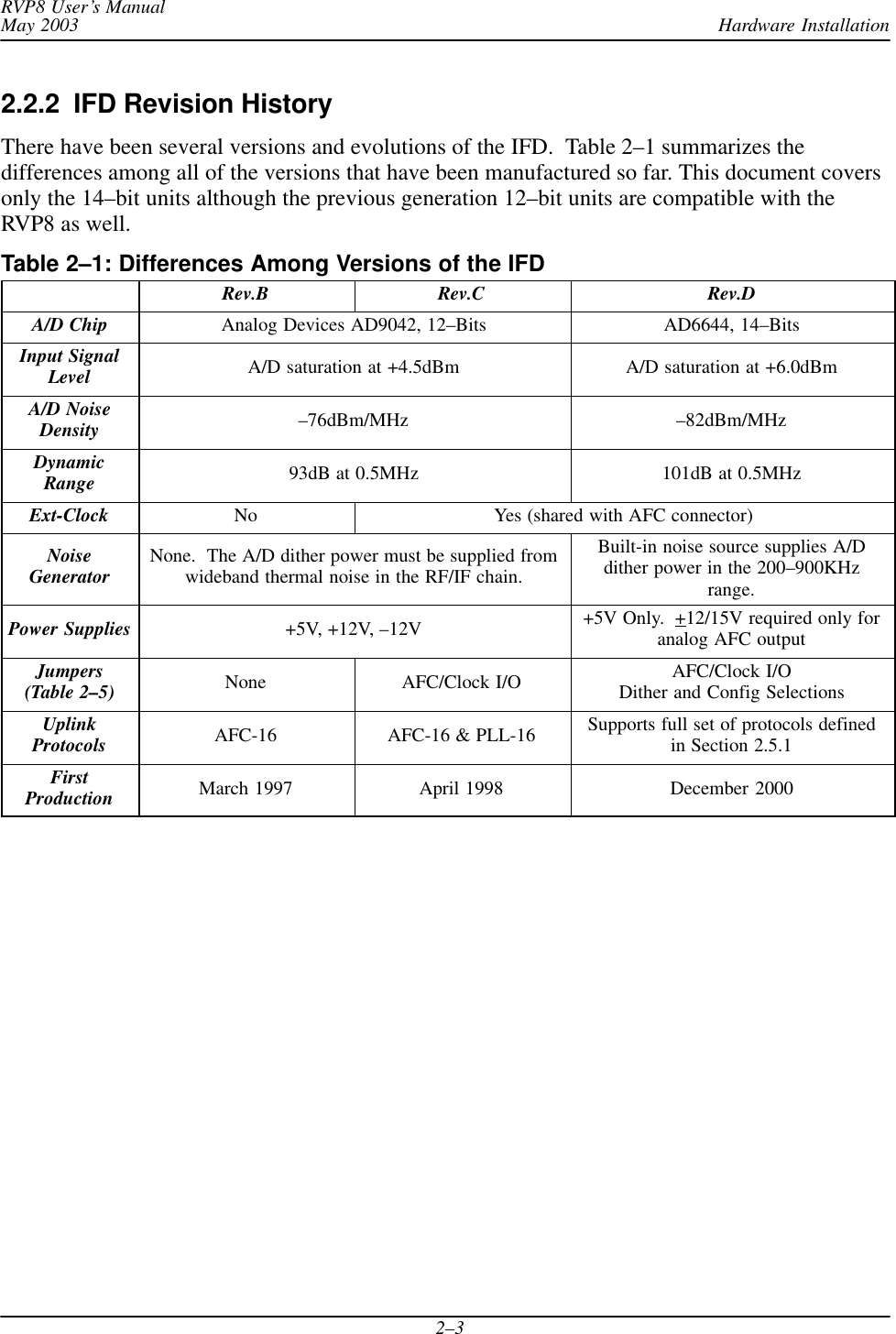
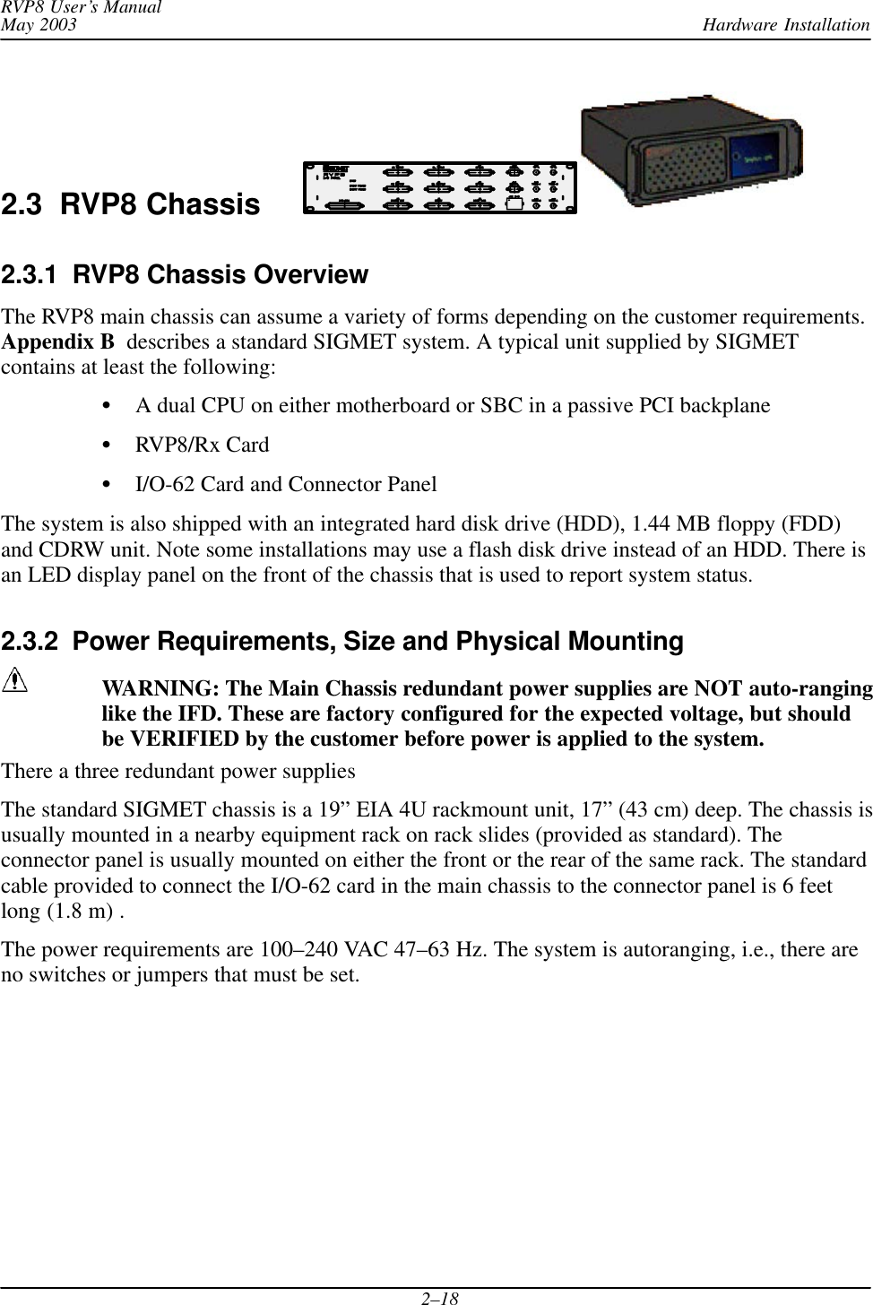
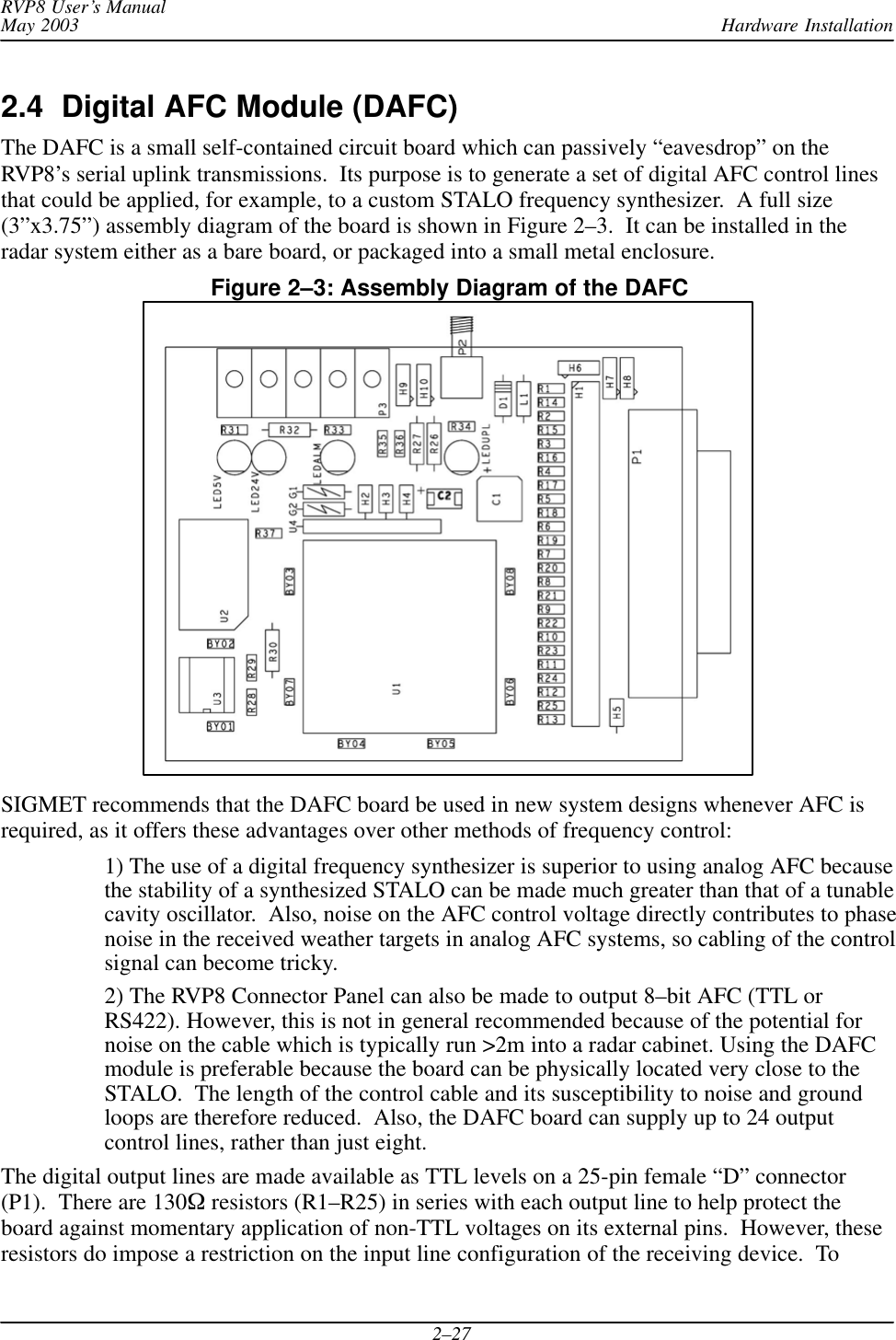
Baron Services XDD-1000C C-BAND DOPPLER WEATHER RADAR User Manual

Baron Services Inc C-BAND DOPPLER WEATHER RADAR

S10 RECEIVER AND PROCESSOR USERS MANUAL PART 1
DRAFT RVP8Digital IF Receiver/Doppler Signal ProcessorUser’s ManualMay 2003 Copyright  2003 SIGMET, Inc.The designs and descriptions contained in this manual may not be copied, translated orreproduced in any form without the prior written consent of SIGMET, Inc.
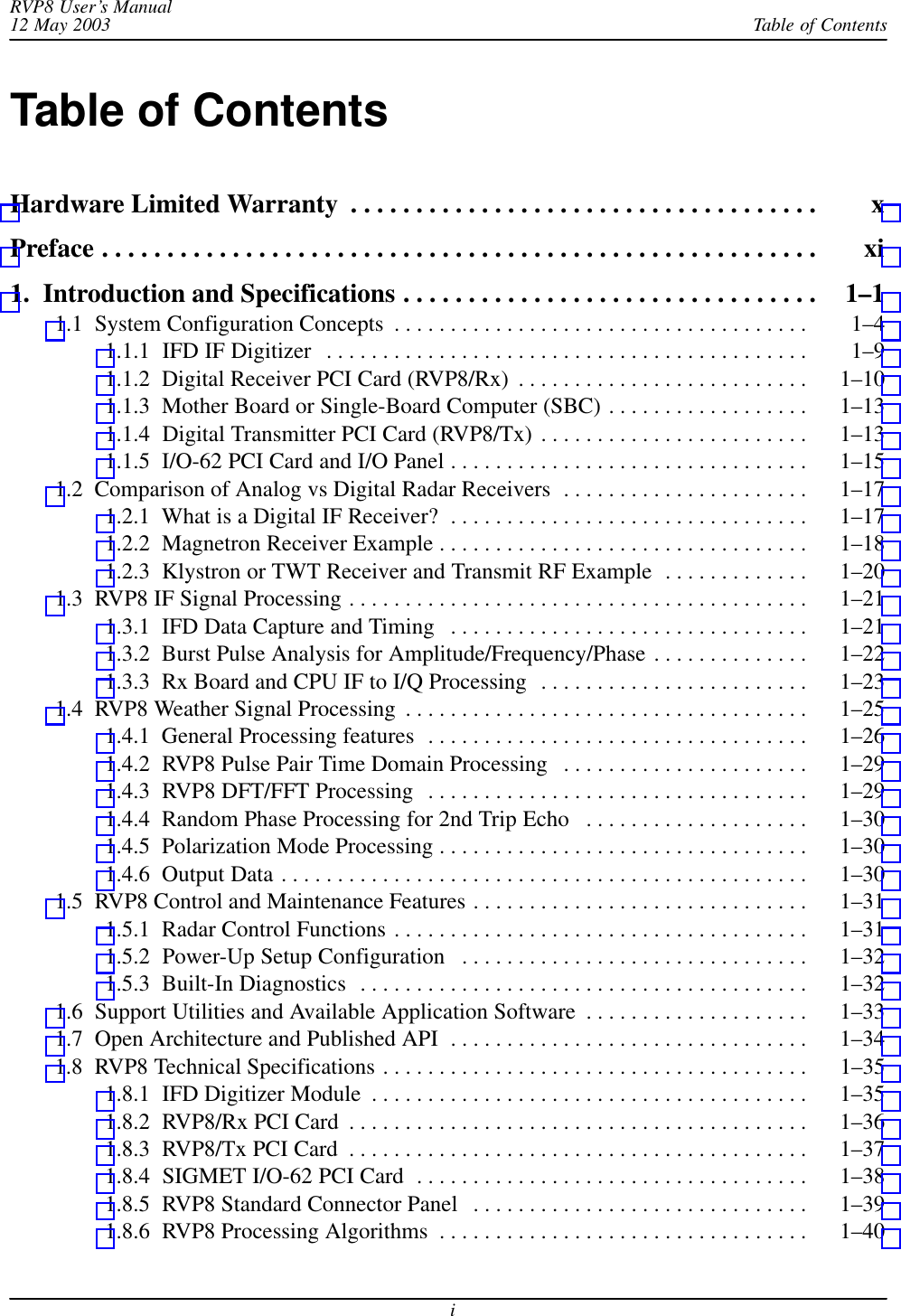
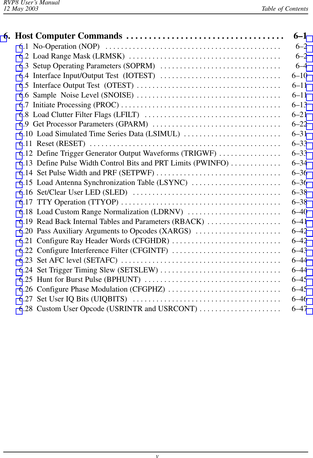
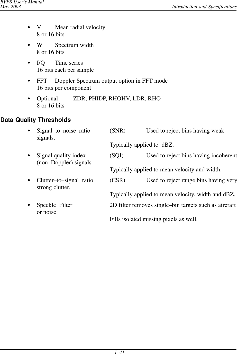
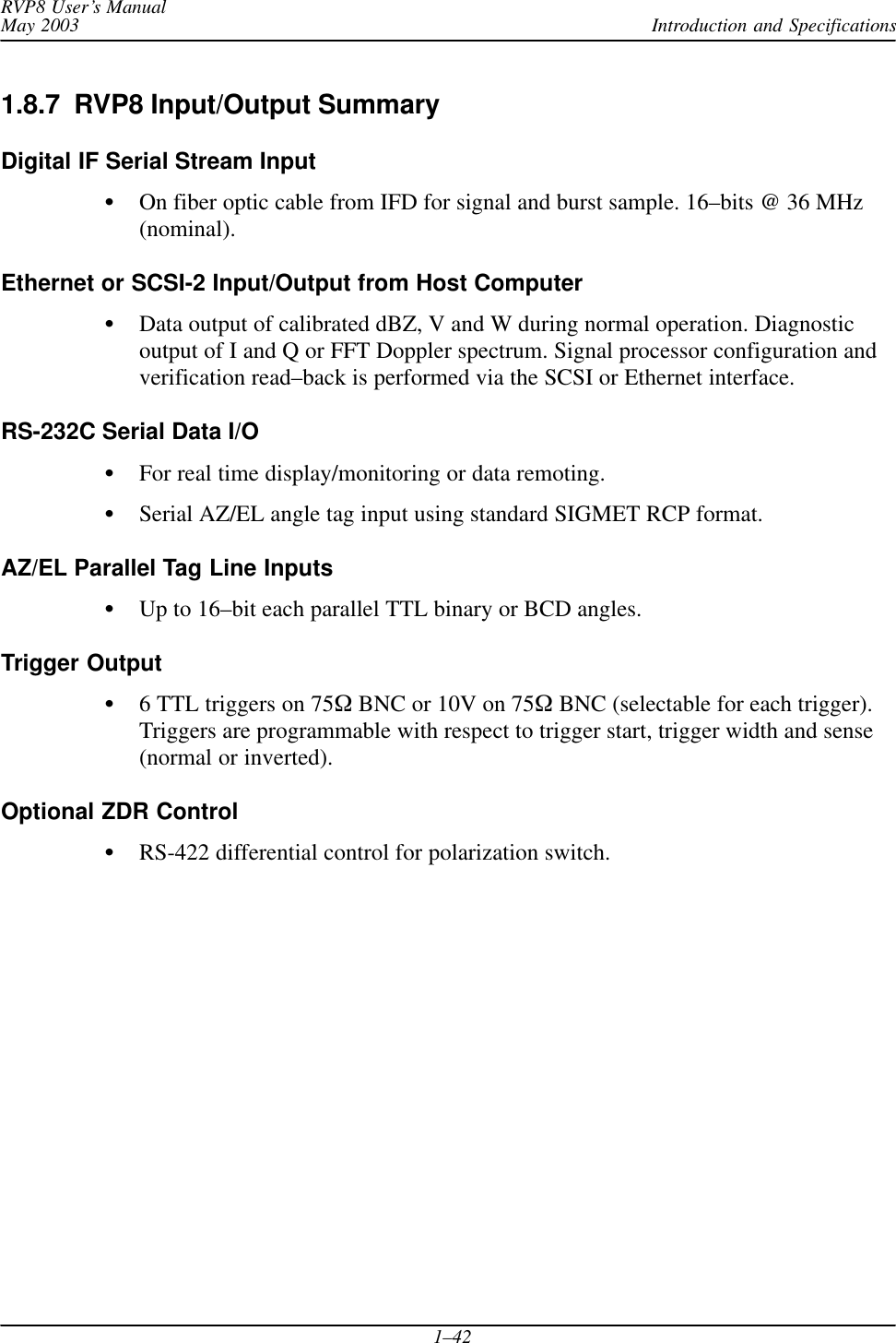
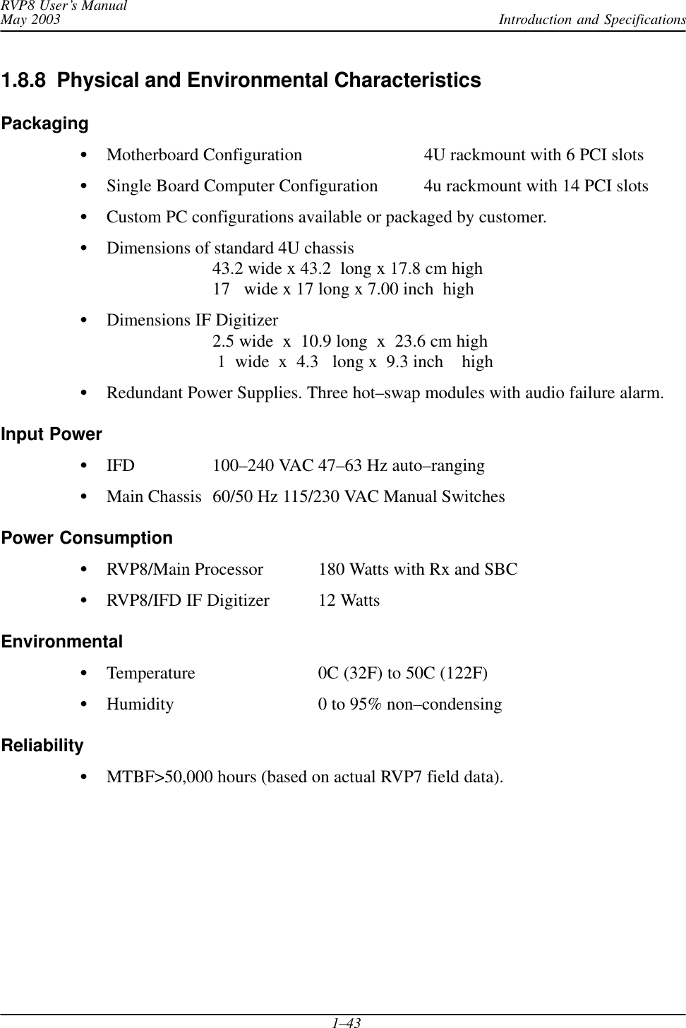
Table of ContentsRVP8 User’s Manual12 May 2003iTable of ContentsHardware Limited Warranty x . . . . . . . . . . . . . . . . . . . . . . . . . . . . . . . . . . . . Preface xi . . . . . . . . . . . . . . . . . . . . . . . . . . . . . . . . . . . . . . . . . . . . . . . . . . . . . . . 1.  Introduction and Specifications 1–1 . . . . . . . . . . . . . . . . . . . . . . . . . . . . . . . . 1.1  System Configuration Concepts 1–4 . . . . . . . . . . . . . . . . . . . . . . . . . . . . . . . . . . . . . 1.1.1  IFD IF Digitizer 1–9 . . . . . . . . . . . . . . . . . . . . . . . . . . . . . . . . . . . . . . . . . . . 1.1.2  Digital Receiver PCI Card (RVP8/Rx) 1–10 . . . . . . . . . . . . . . . . . . . . . . . . . . 1.1.3  Mother Board or Single-Board Computer (SBC) 1–13 . . . . . . . . . . . . . . . . . . 1.1.4  Digital Transmitter PCI Card (RVP8/Tx) 1–13 . . . . . . . . . . . . . . . . . . . . . . . . 1.1.5  I/O-62 PCI Card and I/O Panel 1–15 . . . . . . . . . . . . . . . . . . . . . . . . . . . . . . . . 1.2  Comparison of Analog vs Digital Radar Receivers 1–17 . . . . . . . . . . . . . . . . . . . . . . 1.2.1  What is a Digital IF Receiver? 1–17 . . . . . . . . . . . . . . . . . . . . . . . . . . . . . . . . 1.2.2  Magnetron Receiver Example 1–18 . . . . . . . . . . . . . . . . . . . . . . . . . . . . . . . . . 1.2.3  Klystron or TWT Receiver and Transmit RF Example 1–20 . . . . . . . . . . . . . 1.3  RVP8 IF Signal Processing 1–21 . . . . . . . . . . . . . . . . . . . . . . . . . . . . . . . . . . . . . . . . . 1.3.1  IFD Data Capture and Timing 1–21 . . . . . . . . . . . . . . . . . . . . . . . . . . . . . . . . 1.3.2  Burst Pulse Analysis for Amplitude/Frequency/Phase 1–22 . . . . . . . . . . . . . . 1.3.3  Rx Board and CPU IF to I/Q Processing 1–23 . . . . . . . . . . . . . . . . . . . . . . . . 1.4  RVP8 Weather Signal Processing 1–25 . . . . . . . . . . . . . . . . . . . . . . . . . . . . . . . . . . . . 1.4.1  General Processing features 1–26 . . . . . . . . . . . . . . . . . . . . . . . . . . . . . . . . . . 1.4.2  RVP8 Pulse Pair Time Domain Processing 1–29 . . . . . . . . . . . . . . . . . . . . . . 1.4.3  RVP8 DFT/FFT Processing 1–29 . . . . . . . . . . . . . . . . . . . . . . . . . . . . . . . . . . 1.4.4  Random Phase Processing for 2nd Trip Echo 1–30 . . . . . . . . . . . . . . . . . . . . 1.4.5  Polarization Mode Processing 1–30 . . . . . . . . . . . . . . . . . . . . . . . . . . . . . . . . . 1.4.6  Output Data 1–30 . . . . . . . . . . . . . . . . . . . . . . . . . . . . . . . . . . . . . . . . . . . . . . . 1.5  RVP8 Control and Maintenance Features 1–31 . . . . . . . . . . . . . . . . . . . . . . . . . . . . . . 1.5.1  Radar Control Functions 1–31 . . . . . . . . . . . . . . . . . . . . . . . . . . . . . . . . . . . . . 1.5.2  Power-Up Setup Configuration 1–32 . . . . . . . . . . . . . . . . . . . . . . . . . . . . . . . 1.5.3  Built-In Diagnostics 1–32 . . . . . . . . . . . . . . . . . . . . . . . . . . . . . . . . . . . . . . . . 1.6  Support Utilities and Available Application Software 1–33 . . . . . . . . . . . . . . . . . . . . 1.7  Open Architecture and Published API 1–34 . . . . . . . . . . . . . . . . . . . . . . . . . . . . . . . . 1.8  RVP8 Technical Specifications 1–35 . . . . . . . . . . . . . . . . . . . . . . . . . . . . . . . . . . . . . . 1.8.1  IFD Digitizer Module 1–35 . . . . . . . . . . . . . . . . . . . . . . . . . . . . . . . . . . . . . . . 1.8.2  RVP8/Rx PCI Card 1–36 . . . . . . . . . . . . . . . . . . . . . . . . . . . . . . . . . . . . . . . . . 1.8.3  RVP8/Tx PCI Card 1–37 . . . . . . . . . . . . . . . . . . . . . . . . . . . . . . . . . . . . . . . . . 1.8.4  SIGMET I/O-62 PCI Card 1–38 . . . . . . . . . . . . . . . . . . . . . . . . . . . . . . . . . . . 1.8.5  RVP8 Standard Connector Panel 1–39 . . . . . . . . . . . . . . . . . . . . . . . . . . . . . . 1.8.6  RVP8 Processing Algorithms 1–40 . . . . . . . . . . . . . . . . . . . . . . . . . . . . . . . . .
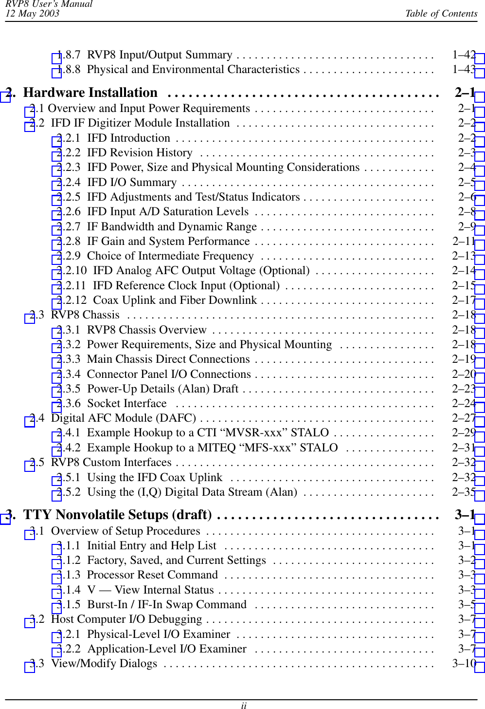
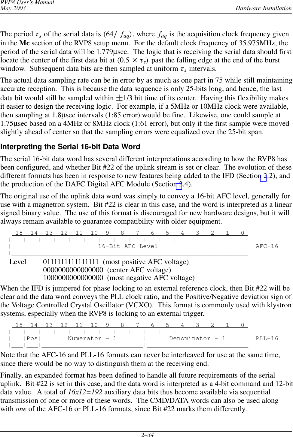
Table of ContentsRVP8 User’s Manual12 May 2003ii1.8.7  RVP8 Input/Output Summary 1–42 . . . . . . . . . . . . . . . . . . . . . . . . . . . . . . . . . 1.8.8  Physical and Environmental Characteristics 1–43 . . . . . . . . . . . . . . . . . . . . . . 2.  Hardware Installation 2–1 . . . . . . . . . . . . . . . . . . . . . . . . . . . . . . . . . . . . . . . 2.1 Overview and Input Power Requirements 2–1 . . . . . . . . . . . . . . . . . . . . . . . . . . . . . . 2.2  IFD IF Digitizer Module Installation 2–2 . . . . . . . . . . . . . . . . . . . . . . . . . . . . . . . . . 2.2.1  IFD Introduction 2–2 . . . . . . . . . . . . . . . . . . . . . . . . . . . . . . . . . . . . . . . . . . . 2.2.2  IFD Revision History 2–3 . . . . . . . . . . . . . . . . . . . . . . . . . . . . . . . . . . . . . . . 2.2.3  IFD Power, Size and Physical Mounting Considerations 2–4 . . . . . . . . . . . . 2.2.4  IFD I/O Summary 2–5 . . . . . . . . . . . . . . . . . . . . . . . . . . . . . . . . . . . . . . . . . . 2.2.5  IFD Adjustments and Test/Status Indicators 2–6 . . . . . . . . . . . . . . . . . . . . . . 2.2.6  IFD Input A/D Saturation Levels 2–8 . . . . . . . . . . . . . . . . . . . . . . . . . . . . . . 2.2.7  IF Bandwidth and Dynamic Range 2–9 . . . . . . . . . . . . . . . . . . . . . . . . . . . . . 2.2.8  IF Gain and System Performance 2–11 . . . . . . . . . . . . . . . . . . . . . . . . . . . . . . 2.2.9  Choice of Intermediate Frequency 2–13 . . . . . . . . . . . . . . . . . . . . . . . . . . . . . 2.2.10  IFD Analog AFC Output Voltage (Optional) 2–14 . . . . . . . . . . . . . . . . . . . . 2.2.11  IFD Reference Clock Input (Optional) 2–15 . . . . . . . . . . . . . . . . . . . . . . . . . 2.2.12  Coax Uplink and Fiber Downlink 2–17 . . . . . . . . . . . . . . . . . . . . . . . . . . . . . 2.3  RVP8 Chassis 2–18 . . . . . . . . . . . . . . . . . . . . . . . . . . . . . . . . . . . . . . . . . . . . . . . . . . . 2.3.1  RVP8 Chassis Overview 2–18 . . . . . . . . . . . . . . . . . . . . . . . . . . . . . . . . . . . . . 2.3.2  Power Requirements, Size and Physical Mounting 2–18 . . . . . . . . . . . . . . . . 2.3.3  Main Chassis Direct Connections 2–19 . . . . . . . . . . . . . . . . . . . . . . . . . . . . . . 2.3.4  Connector Panel I/O Connections 2–20 . . . . . . . . . . . . . . . . . . . . . . . . . . . . . . 2.3.5  Power-Up Details (Alan) Draft 2–23 . . . . . . . . . . . . . . . . . . . . . . . . . . . . . . . . 2.3.6  Socket Interface 2–24 . . . . . . . . . . . . . . . . . . . . . . . . . . . . . . . . . . . . . . . . . . . 2.4  Digital AFC Module (DAFC) 2–27 . . . . . . . . . . . . . . . . . . . . . . . . . . . . . . . . . . . . . . . 2.4.1  Example Hookup to a CTI “MVSR-xxx” STALO 2–29 . . . . . . . . . . . . . . . . . 2.4.2  Example Hookup to a MITEQ “MFS-xxx” STALO 2–31 . . . . . . . . . . . . . . . 2.5  RVP8 Custom Interfaces 2–32 . . . . . . . . . . . . . . . . . . . . . . . . . . . . . . . . . . . . . . . . . . . 2.5.1  Using the IFD Coax Uplink 2–32 . . . . . . . . . . . . . . . . . . . . . . . . . . . . . . . . . . 2.5.2  Using the (I,Q) Digital Data Stream (Alan) 2–35 . . . . . . . . . . . . . . . . . . . . . . 3.  TTY Nonvolatile Setups (draft) 3–1 . . . . . . . . . . . . . . . . . . . . . . . . . . . . . . . . 3.1  Overview of Setup Procedures 3–1 . . . . . . . . . . . . . . . . . . . . . . . . . . . . . . . . . . . . . . 3.1.1  Initial Entry and Help List 3–1 . . . . . . . . . . . . . . . . . . . . . . . . . . . . . . . . . . . 3.1.2  Factory, Saved, and Current Settings 3–2 . . . . . . . . . . . . . . . . . . . . . . . . . . . 3.1.3  Processor Reset Command 3–3 . . . . . . . . . . . . . . . . . . . . . . . . . . . . . . . . . . . 3.1.4  V — View Internal Status 3–3 . . . . . . . . . . . . . . . . . . . . . . . . . . . . . . . . . . . . 3.1.5  Burst-In / IF-In Swap Command 3–5 . . . . . . . . . . . . . . . . . . . . . . . . . . . . . . 3.2  Host Computer I/O Debugging 3–7 . . . . . . . . . . . . . . . . . . . . . . . . . . . . . . . . . . . . . . 3.2.1  Physical-Level I/O Examiner 3–7 . . . . . . . . . . . . . . . . . . . . . . . . . . . . . . . . . 3.2.2  Application-Level I/O Examiner 3–7 . . . . . . . . . . . . . . . . . . . . . . . . . . . . . . 3.3  View/Modify Dialogs 3–10 . . . . . . . . . . . . . . . . . . . . . . . . . . . . . . . . . . . . . . . . . . . . .
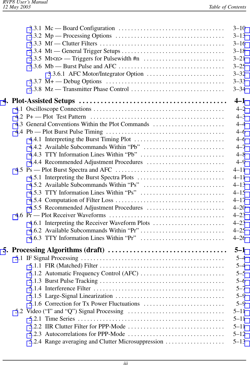
Table of ContentsRVP8 User’s Manual12 May 2003iii3.3.1  Mc — Board Configuration 3–10 . . . . . . . . . . . . . . . . . . . . . . . . . . . . . . . . . . 3.3.2  Mp — Processing Options 3–13 . . . . . . . . . . . . . . . . . . . . . . . . . . . . . . . . . . . 3.3.3  Mf — Clutter Filters 3–16 . . . . . . . . . . . . . . . . . . . . . . . . . . . . . . . . . . . . . . . . 3.3.4  Mt — General Trigger Setups 3–18 . . . . . . . . . . . . . . . . . . . . . . . . . . . . . . . . . 3.3.5  Mt<n> — Triggers for Pulsewidth #n 3–21 . . . . . . . . . . . . . . . . . . . . . . . . . . 3.3.6  Mb — Burst Pulse and AFC 3–25 . . . . . . . . . . . . . . . . . . . . . . . . . . . . . . . . . . 3.3.6.1  AFC Motor/Integrator Option 3–32 . . . . . . . . . . . . . . . . . . . . . . . . . 3.3.7  M+ — Debug Options 3–33 . . . . . . . . . . . . . . . . . . . . . . . . . . . . . . . . . . . . . . 3.3.8  Mz — Transmitter Phase Control 3–34 . . . . . . . . . . . . . . . . . . . . . . . . . . . . . . 4.  Plot-Assisted Setups 4–1 . . . . . . . . . . . . . . . . . . . . . . . . . . . . . . . . . . . . . . . . . 4.1  Oscilloscope Connections 4–2 . . . . . . . . . . . . . . . . . . . . . . . . . . . . . . . . . . . . . . . . . . 4.2  P+ — Plot  Test Pattern 4–3 . . . . . . . . . . . . . . . . . . . . . . . . . . . . . . . . . . . . . . . . . . . 4.3  General Conventions Within the Plot Commands 4–4 . . . . . . . . . . . . . . . . . . . . . . . 4.4  Pb — Plot Burst Pulse Timing 4–6 . . . . . . . . . . . . . . . . . . . . . . . . . . . . . . . . . . . . . . 4.4.1  Interpreting the Burst Timing Plot 4–6 . . . . . . . . . . . . . . . . . . . . . . . . . . . . . 4.4.2  Available Subcommands Within “Pb” 4–7 . . . . . . . . . . . . . . . . . . . . . . . . . . 4.4.3  TTY Information Lines Within “Pb” 4–8 . . . . . . . . . . . . . . . . . . . . . . . . . . . 4.4.4  Recommended Adjustment Procedures 4–9 . . . . . . . . . . . . . . . . . . . . . . . . . 4.5  Ps — Plot Burst Spectra and AFC 4–11 . . . . . . . . . . . . . . . . . . . . . . . . . . . . . . . . . . . 4.5.1  Interpreting the Burst Spectra Plots 4–11 . . . . . . . . . . . . . . . . . . . . . . . . . . . . 4.5.2  Available Subcommands Within “Ps” 4–13 . . . . . . . . . . . . . . . . . . . . . . . . . . 4.5.3  TTY Information Lines Within “Ps” 4–15 . . . . . . . . . . . . . . . . . . . . . . . . . . . 4.5.4  Computation of Filter Loss 4–17 . . . . . . . . . . . . . . . . . . . . . . . . . . . . . . . . . . . 4.5.5  Recommended Adjustment Procedures 4–20 . . . . . . . . . . . . . . . . . . . . . . . . . 4.6  Pr — Plot Receiver Waveforms 4–23 . . . . . . . . . . . . . . . . . . . . . . . . . . . . . . . . . . . . . 4.6.1  Interpreting the Receiver Waveform Plots 4–23 . . . . . . . . . . . . . . . . . . . . . . . 4.6.2  Available Subcommands Within “Pr” 4–25 . . . . . . . . . . . . . . . . . . . . . . . . . . . 4.6.3  TTY Information Lines Within “Pr” 4–26 . . . . . . . . . . . . . . . . . . . . . . . . . . . 5.  Processing Algorithms (draft) 5–1 . . . . . . . . . . . . . . . . . . . . . . . . . . . . . . . . . 5.1  IF Signal Processing 5–4 . . . . . . . . . . . . . . . . . . . . . . . . . . . . . . . . . . . . . . . . . . . . . . 5.1.1  FIR (Matched) Filter 5–4 . . . . . . . . . . . . . . . . . . . . . . . . . . . . . . . . . . . . . . . . 5.1.2  Automatic Frequency Control (AFC) 5–5 . . . . . . . . . . . . . . . . . . . . . . . . . . . 5.1.3  Burst Pulse Tracking 5–6 . . . . . . . . . . . . . . . . . . . . . . . . . . . . . . . . . . . . . . . . 5.1.4  Interference Filter 5–7 . . . . . . . . . . . . . . . . . . . . . . . . . . . . . . . . . . . . . . . . . . 5.1.5  Large-Signal Linearization 5–9 . . . . . . . . . . . . . . . . . . . . . . . . . . . . . . . . . . . 5.1.6  Correction for Tx Power Fluctuations 5–9 . . . . . . . . . . . . . . . . . . . . . . . . . . 5.2  Video (“I” and “Q”) Signal Processing 5–11 . . . . . . . . . . . . . . . . . . . . . . . . . . . . . . . 5.2.1  Time Series 5–11 . . . . . . . . . . . . . . . . . . . . . . . . . . . . . . . . . . . . . . . . . . . . . . . 5.2.2  IIR Clutter Filter for PPP-Mode 5–11 . . . . . . . . . . . . . . . . . . . . . . . . . . . . . . . 5.2.3  Autocorrelations for PPP-Mode 5–12 . . . . . . . . . . . . . . . . . . . . . . . . . . . . . . . 5.2.4  Range averaging and Clutter Microsuppression 5–13 . . . . . . . . . . . . . . . . . . .
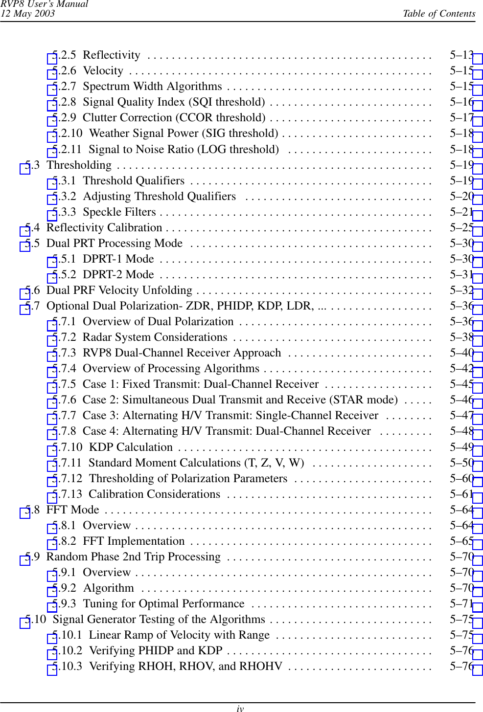
Table of ContentsRVP8 User’s Manual12 May 2003iv5.2.5  Reflectivity 5–13 . . . . . . . . . . . . . . . . . . . . . . . . . . . . . . . . . . . . . . . . . . . . . . . 5.2.6  Velocity 5–15 . . . . . . . . . . . . . . . . . . . . . . . . . . . . . . . . . . . . . . . . . . . . . . . . . . 5.2.7  Spectrum Width Algorithms 5–15 . . . . . . . . . . . . . . . . . . . . . . . . . . . . . . . . . . 5.2.8  Signal Quality Index (SQI threshold) 5–16 . . . . . . . . . . . . . . . . . . . . . . . . . . . 5.2.9  Clutter Correction (CCOR threshold) 5–17 . . . . . . . . . . . . . . . . . . . . . . . . . . . 5.2.10  Weather Signal Power (SIG threshold) 5–18 . . . . . . . . . . . . . . . . . . . . . . . . . 5.2.11  Signal to Noise Ratio (LOG threshold) 5–18 . . . . . . . . . . . . . . . . . . . . . . . . 5.3  Thresholding 5–19 . . . . . . . . . . . . . . . . . . . . . . . . . . . . . . . . . . . . . . . . . . . . . . . . . . . . 5.3.1  Threshold Qualifiers 5–19 . . . . . . . . . . . . . . . . . . . . . . . . . . . . . . . . . . . . . . . . 5.3.2  Adjusting Threshold Qualifiers 5–20 . . . . . . . . . . . . . . . . . . . . . . . . . . . . . . . 5.3.3  Speckle Filters 5–21 . . . . . . . . . . . . . . . . . . . . . . . . . . . . . . . . . . . . . . . . . . . . . 5.4  Reflectivity Calibration 5–25 . . . . . . . . . . . . . . . . . . . . . . . . . . . . . . . . . . . . . . . . . . . . 5.5  Dual PRT Processing Mode 5–30 . . . . . . . . . . . . . . . . . . . . . . . . . . . . . . . . . . . . . . . . 5.5.1  DPRT-1 Mode 5–30 . . . . . . . . . . . . . . . . . . . . . . . . . . . . . . . . . . . . . . . . . . . . . 5.5.2  DPRT-2 Mode 5–31 . . . . . . . . . . . . . . . . . . . . . . . . . . . . . . . . . . . . . . . . . . . . . 5.6  Dual PRF Velocity Unfolding 5–32 . . . . . . . . . . . . . . . . . . . . . . . . . . . . . . . . . . . . . . . 5.7  Optional Dual Polarization- ZDR, PHIDP, KDP, LDR, ... 5–36 . . . . . . . . . . . . . . . . . 5.7.1  Overview of Dual Polarization 5–36 . . . . . . . . . . . . . . . . . . . . . . . . . . . . . . . . 5.7.2  Radar System Considerations 5–38 . . . . . . . . . . . . . . . . . . . . . . . . . . . . . . . . . 5.7.3  RVP8 Dual-Channel Receiver Approach 5–40 . . . . . . . . . . . . . . . . . . . . . . . . 5.7.4  Overview of Processing Algorithms 5–42 . . . . . . . . . . . . . . . . . . . . . . . . . . . . 5.7.5  Case 1: Fixed Transmit: Dual-Channel Receiver 5–45 . . . . . . . . . . . . . . . . . . 5.7.6  Case 2: Simultaneous Dual Transmit and Receive (STAR mode) 5–46 . . . . . 5.7.7  Case 3: Alternating H/V Transmit: Single-Channel Receiver 5–47 . . . . . . . . 5.7.8  Case 4: Alternating H/V Transmit: Dual-Channel Receiver 5–48 . . . . . . . . . 5.7.10  KDP Calculation 5–49 . . . . . . . . . . . . . . . . . . . . . . . . . . . . . . . . . . . . . . . . . . 5.7.11  Standard Moment Calculations (T, Z, V, W) 5–50 . . . . . . . . . . . . . . . . . . . . 5.7.12  Thresholding of Polarization Parameters 5–60 . . . . . . . . . . . . . . . . . . . . . . . 5.7.13  Calibration Considerations 5–61 . . . . . . . . . . . . . . . . . . . . . . . . . . . . . . . . . . 5.8  FFT Mode 5–64 . . . . . . . . . . . . . . . . . . . . . . . . . . . . . . . . . . . . . . . . . . . . . . . . . . . . . . 5.8.1  Overview 5–64 . . . . . . . . . . . . . . . . . . . . . . . . . . . . . . . . . . . . . . . . . . . . . . . . . 5.8.2  FFT Implementation 5–65 . . . . . . . . . . . . . . . . . . . . . . . . . . . . . . . . . . . . . . . . 5.9  Random Phase 2nd Trip Processing 5–70 . . . . . . . . . . . . . . . . . . . . . . . . . . . . . . . . . . 5.9.1  Overview 5–70 . . . . . . . . . . . . . . . . . . . . . . . . . . . . . . . . . . . . . . . . . . . . . . . . . 5.9.2  Algorithm 5–70 . . . . . . . . . . . . . . . . . . . . . . . . . . . . . . . . . . . . . . . . . . . . . . . . 5.9.3  Tuning for Optimal Performance 5–71 . . . . . . . . . . . . . . . . . . . . . . . . . . . . . . 5.10  Signal Generator Testing of the Algorithms 5–75 . . . . . . . . . . . . . . . . . . . . . . . . . . . 5.10.1  Linear Ramp of Velocity with Range 5–75 . . . . . . . . . . . . . . . . . . . . . . . . . . 5.10.2  Verifying PHIDP and KDP 5–76 . . . . . . . . . . . . . . . . . . . . . . . . . . . . . . . . . . 5.10.3  Verifying RHOH, RHOV, and RHOHV 5–76 . . . . . . . . . . . . . . . . . . . . . . . .
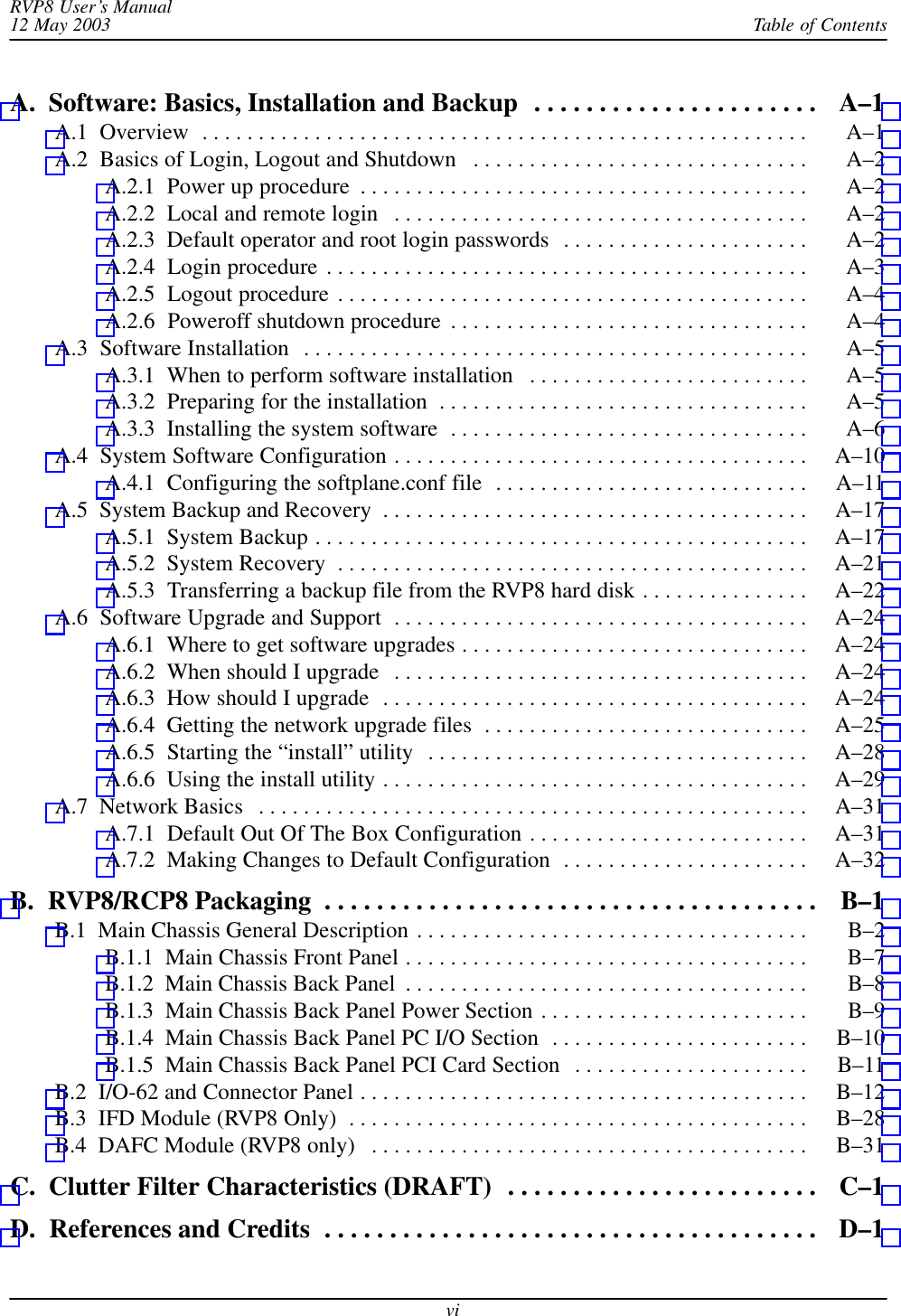
Table of ContentsRVP8 User’s Manual12 May 2003v6.  Host Computer Commands 6–1 . . . . . . . . . . . . . . . . . . . . . . . . . . . . . . . . . . . 6.1  No-Operation (NOP) 6–2 . . . . . . . . . . . . . . . . . . . . . . . . . . . . . . . . . . . . . . . . . . . . . 6.2  Load Range Mask (LRMSK) 6–2 . . . . . . . . . . . . . . . . . . . . . . . . . . . . . . . . . . . . . . . 6.3  Setup Operating Parameters (SOPRM) 6–4 . . . . . . . . . . . . . . . . . . . . . . . . . . . . . . . 6.4  Interface Input/Output Test  (IOTEST) 6–10 . . . . . . . . . . . . . . . . . . . . . . . . . . . . . . . 6.5  Interface Output Test  (OTEST) 6–11 . . . . . . . . . . . . . . . . . . . . . . . . . . . . . . . . . . . . . 6.6  Sample  Noise Level (SNOISE) 6–11 . . . . . . . . . . . . . . . . . . . . . . . . . . . . . . . . . . . . . 6.7  Initiate Processing (PROC) 6–13 . . . . . . . . . . . . . . . . . . . . . . . . . . . . . . . . . . . . . . . . . 6.8  Load Clutter Filter Flags (LFILT) 6–21 . . . . . . . . . . . . . . . . . . . . . . . . . . . . . . . . . . . 6.9  Get Processor Parameters (GPARM) 6–22 . . . . . . . . . . . . . . . . . . . . . . . . . . . . . . . . . 6.10  Load Simulated Time Series Data (LSIMUL) 6–31 . . . . . . . . . . . . . . . . . . . . . . . . . 6.11  Reset (RESET) 6–33 . . . . . . . . . . . . . . . . . . . . . . . . . . . . . . . . . . . . . . . . . . . . . . . . . 6.12  Define Trigger Generator Output Waveforms (TRIGWF) 6–33 . . . . . . . . . . . . . . . . 6.13  Define Pulse Width Control Bits and PRT Limits (PWINFO) 6–34 . . . . . . . . . . . . . 6.14  Set Pulse Width and PRF (SETPWF) 6–36 . . . . . . . . . . . . . . . . . . . . . . . . . . . . . . . . 6.15  Load Antenna Synchronization Table (LSYNC) 6–36 . . . . . . . . . . . . . . . . . . . . . . . 6.16  Set/Clear User LED (SLED) 6–38 . . . . . . . . . . . . . . . . . . . . . . . . . . . . . . . . . . . . . . 6.17  TTY Operation (TTYOP) 6–38 . . . . . . . . . . . . . . . . . . . . . . . . . . . . . . . . . . . . . . . . . 6.18  Load Custom Range Normalization (LDRNV) 6–40 . . . . . . . . . . . . . . . . . . . . . . . . 6.19  Read Back Internal Tables and Parameters (RBACK) 6–41 . . . . . . . . . . . . . . . . . . . 6.20  Pass Auxiliary Arguments to Opcodes (XARGS) 6–42 . . . . . . . . . . . . . . . . . . . . . . 6.21  Configure Ray Header Words (CFGHDR) 6–42 . . . . . . . . . . . . . . . . . . . . . . . . . . . . 6.22  Configure Interference Filter (CFGINTF) 6–43 . . . . . . . . . . . . . . . . . . . . . . . . . . . . 6.23  Set AFC level (SETAFC) 6–44 . . . . . . . . . . . . . . . . . . . . . . . . . . . . . . . . . . . . . . . . . 6.24  Set Trigger Timing Slew (SETSLEW) 6–44 . . . . . . . . . . . . . . . . . . . . . . . . . . . . . . . 6.25  Hunt for Burst Pulse (BPHUNT) 6–45 . . . . . . . . . . . . . . . . . . . . . . . . . . . . . . . . . . . 6.26  Configure Phase Modulation (CFGPHZ) 6–45 . . . . . . . . . . . . . . . . . . . . . . . . . . . . . 6.27  Set User IQ Bits (UIQBITS) 6–46 . . . . . . . . . . . . . . . . . . . . . . . . . . . . . . . . . . . . . . 6.28  Custom User Opcode (USRINTR and USRCONT) 6–47 . . . . . . . . . . . . . . . . . . . . .
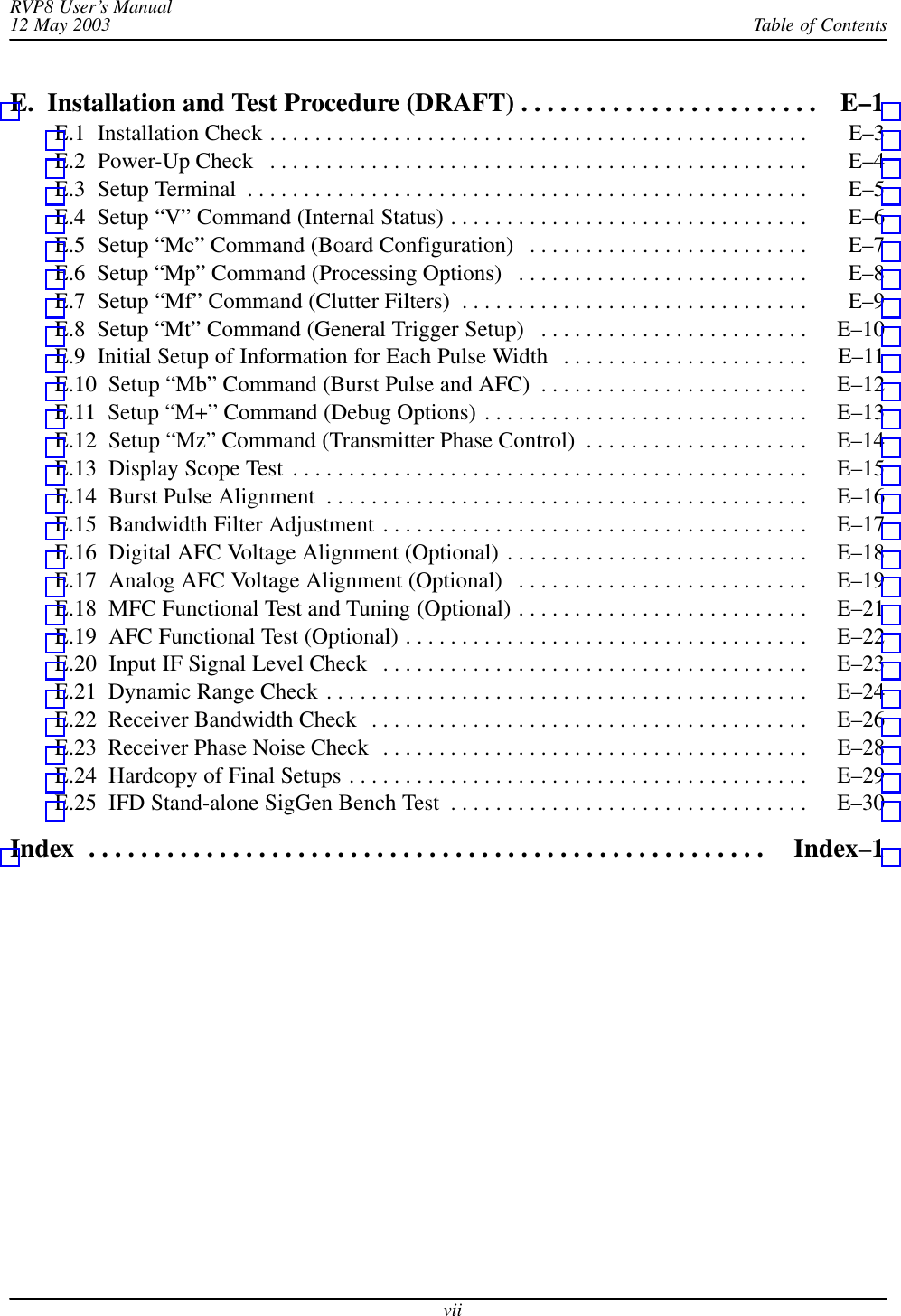
Table of ContentsRVP8 User’s Manual12 May 2003viA.  Software: Basics, Installation and Backup A–1 . . . . . . . . . . . . . . . . . . . . . . A.1  Overview A–1 . . . . . . . . . . . . . . . . . . . . . . . . . . . . . . . . . . . . . . . . . . . . . . . . . . . . . . A.2  Basics of Login, Logout and Shutdown A–2 . . . . . . . . . . . . . . . . . . . . . . . . . . . . . . A.2.1  Power up procedure A–2 . . . . . . . . . . . . . . . . . . . . . . . . . . . . . . . . . . . . . . . . A.2.2  Local and remote login A–2 . . . . . . . . . . . . . . . . . . . . . . . . . . . . . . . . . . . . . A.2.3  Default operator and root login passwords A–2 . . . . . . . . . . . . . . . . . . . . . . A.2.4  Login procedure A–3 . . . . . . . . . . . . . . . . . . . . . . . . . . . . . . . . . . . . . . . . . . . A.2.5  Logout procedure A–4 . . . . . . . . . . . . . . . . . . . . . . . . . . . . . . . . . . . . . . . . . . A.2.6  Poweroff shutdown procedure A–4 . . . . . . . . . . . . . . . . . . . . . . . . . . . . . . . . A.3  Software Installation A–5 . . . . . . . . . . . . . . . . . . . . . . . . . . . . . . . . . . . . . . . . . . . . . A.3.1  When to perform software installation A–5 . . . . . . . . . . . . . . . . . . . . . . . . . A.3.2  Preparing for the installation A–5 . . . . . . . . . . . . . . . . . . . . . . . . . . . . . . . . . A.3.3  Installing the system software A–6 . . . . . . . . . . . . . . . . . . . . . . . . . . . . . . . . A.4  System Software Configuration A–10 . . . . . . . . . . . . . . . . . . . . . . . . . . . . . . . . . . . . . A.4.1  Configuring the softplane.conf file A–11 . . . . . . . . . . . . . . . . . . . . . . . . . . . . A.5  System Backup and Recovery A–17 . . . . . . . . . . . . . . . . . . . . . . . . . . . . . . . . . . . . . . A.5.1  System Backup A–17 . . . . . . . . . . . . . . . . . . . . . . . . . . . . . . . . . . . . . . . . . . . . A.5.2  System Recovery A–21 . . . . . . . . . . . . . . . . . . . . . . . . . . . . . . . . . . . . . . . . . . A.5.3  Transferring a backup file from the RVP8 hard disk A–22 . . . . . . . . . . . . . . . A.6  Software Upgrade and Support A–24 . . . . . . . . . . . . . . . . . . . . . . . . . . . . . . . . . . . . . A.6.1  Where to get software upgrades A–24 . . . . . . . . . . . . . . . . . . . . . . . . . . . . . . . A.6.2  When should I upgrade A–24 . . . . . . . . . . . . . . . . . . . . . . . . . . . . . . . . . . . . . A.6.3  How should I upgrade A–24 . . . . . . . . . . . . . . . . . . . . . . . . . . . . . . . . . . . . . . A.6.4  Getting the network upgrade files A–25 . . . . . . . . . . . . . . . . . . . . . . . . . . . . . A.6.5  Starting the “install” utility A–28 . . . . . . . . . . . . . . . . . . . . . . . . . . . . . . . . . . A.6.6  Using the install utility A–29 . . . . . . . . . . . . . . . . . . . . . . . . . . . . . . . . . . . . . . A.7  Network Basics A–31 . . . . . . . . . . . . . . . . . . . . . . . . . . . . . . . . . . . . . . . . . . . . . . . . . A.7.1  Default Out Of The Box Configuration A–31 . . . . . . . . . . . . . . . . . . . . . . . . . A.7.2  Making Changes to Default Configuration A–32 . . . . . . . . . . . . . . . . . . . . . . B.  RVP8/RCP8 Packaging B–1 . . . . . . . . . . . . . . . . . . . . . . . . . . . . . . . . . . . . . . B.1  Main Chassis General Description B–2 . . . . . . . . . . . . . . . . . . . . . . . . . . . . . . . . . . . B.1.1  Main Chassis Front Panel B–7 . . . . . . . . . . . . . . . . . . . . . . . . . . . . . . . . . . . . B.1.2  Main Chassis Back Panel B–8 . . . . . . . . . . . . . . . . . . . . . . . . . . . . . . . . . . . . B.1.3  Main Chassis Back Panel Power Section B–9 . . . . . . . . . . . . . . . . . . . . . . . . B.1.4  Main Chassis Back Panel PC I/O Section B–10 . . . . . . . . . . . . . . . . . . . . . . . B.1.5  Main Chassis Back Panel PCI Card Section B–11 . . . . . . . . . . . . . . . . . . . . . B.2  I/O-62 and Connector Panel B–12 . . . . . . . . . . . . . . . . . . . . . . . . . . . . . . . . . . . . . . . . B.3  IFD Module (RVP8 Only) B–28 . . . . . . . . . . . . . . . . . . . . . . . . . . . . . . . . . . . . . . . . . B.4  DAFC Module (RVP8 only) B–31 . . . . . . . . . . . . . . . . . . . . . . . . . . . . . . . . . . . . . . . C.  Clutter Filter Characteristics (DRAFT) C–1 . . . . . . . . . . . . . . . . . . . . . . . . D.  References and Credits D–1 . . . . . . . . . . . . . . . . . . . . . . . . . . . . . . . . . . . . . .
Table of ContentsRVP8 User’s Manual12 May 2003viiE.  Installation and Test Procedure (DRAFT) E–1 . . . . . . . . . . . . . . . . . . . . . . . E.1  Installation Check E–3 . . . . . . . . . . . . . . . . . . . . . . . . . . . . . . . . . . . . . . . . . . . . . . . . E.2  Power-Up Check E–4 . . . . . . . . . . . . . . . . . . . . . . . . . . . . . . . . . . . . . . . . . . . . . . . . E.3  Setup Terminal E–5 . . . . . . . . . . . . . . . . . . . . . . . . . . . . . . . . . . . . . . . . . . . . . . . . . . E.4  Setup “V” Command (Internal Status) E–6 . . . . . . . . . . . . . . . . . . . . . . . . . . . . . . . . E.5  Setup “Mc” Command (Board Configuration) E–7 . . . . . . . . . . . . . . . . . . . . . . . . . E.6  Setup “Mp” Command (Processing Options) E–8 . . . . . . . . . . . . . . . . . . . . . . . . . . E.7  Setup “Mf” Command (Clutter Filters) E–9 . . . . . . . . . . . . . . . . . . . . . . . . . . . . . . . E.8  Setup “Mt” Command (General Trigger Setup) E–10 . . . . . . . . . . . . . . . . . . . . . . . . E.9  Initial Setup of Information for Each Pulse Width E–11 . . . . . . . . . . . . . . . . . . . . . . E.10  Setup “Mb” Command (Burst Pulse and AFC) E–12 . . . . . . . . . . . . . . . . . . . . . . . . E.11  Setup “M+” Command (Debug Options) E–13 . . . . . . . . . . . . . . . . . . . . . . . . . . . . . E.12  Setup “Mz” Command (Transmitter Phase Control) E–14 . . . . . . . . . . . . . . . . . . . . E.13  Display Scope Test E–15 . . . . . . . . . . . . . . . . . . . . . . . . . . . . . . . . . . . . . . . . . . . . . . E.14  Burst Pulse Alignment E–16 . . . . . . . . . . . . . . . . . . . . . . . . . . . . . . . . . . . . . . . . . . . E.15  Bandwidth Filter Adjustment E–17 . . . . . . . . . . . . . . . . . . . . . . . . . . . . . . . . . . . . . . E.16  Digital AFC Voltage Alignment (Optional) E–18 . . . . . . . . . . . . . . . . . . . . . . . . . . . E.17  Analog AFC Voltage Alignment (Optional) E–19 . . . . . . . . . . . . . . . . . . . . . . . . . . E.18  MFC Functional Test and Tuning (Optional) E–21 . . . . . . . . . . . . . . . . . . . . . . . . . . E.19  AFC Functional Test (Optional) E–22 . . . . . . . . . . . . . . . . . . . . . . . . . . . . . . . . . . . . E.20  Input IF Signal Level Check E–23 . . . . . . . . . . . . . . . . . . . . . . . . . . . . . . . . . . . . . . E.21  Dynamic Range Check E–24 . . . . . . . . . . . . . . . . . . . . . . . . . . . . . . . . . . . . . . . . . . . E.22  Receiver Bandwidth Check E–26 . . . . . . . . . . . . . . . . . . . . . . . . . . . . . . . . . . . . . . . E.23  Receiver Phase Noise Check E–28 . . . . . . . . . . . . . . . . . . . . . . . . . . . . . . . . . . . . . . E.24  Hardcopy of Final Setups E–29 . . . . . . . . . . . . . . . . . . . . . . . . . . . . . . . . . . . . . . . . . E.25  IFD Stand-alone SigGen Bench Test E–30 . . . . . . . . . . . . . . . . . . . . . . . . . . . . . . . . Index Index–1 . . . . . . . . . . . . . . . . . . . . . . . . . . . . . . . . . . . . . . . . . . . . . . . . . . . .
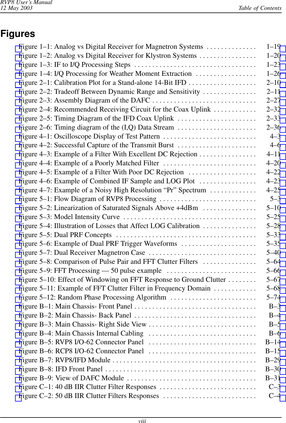
Table of ContentsRVP8 User’s Manual12 May 2003viiiFiguresFigure 1–1: Analog vs Digital Receiver for Magnetron Systems 1–19 . . . . . . . . . . . . . . Figure 1–2: Analog vs Digital Receiver for Klystron Systems 1–20 . . . . . . . . . . . . . . . . Figure 1–3: IF to I/Q Processing Steps 1–23 . . . . . . . . . . . . . . . . . . . . . . . . . . . . . . . . . . Figure 1–4: I/Q Processing for Weather Moment Extraction 1–26 . . . . . . . . . . . . . . . . . Figure 2–1: Calibration Plot for a Stand-alone 14-Bit IFD 2–10 . . . . . . . . . . . . . . . . . . . Figure 2–2: Tradeoff Between Dynamic Range and Sensitivity 2–11 . . . . . . . . . . . . . . . Figure 2–3: Assembly Diagram of the DAFC 2–27 . . . . . . . . . . . . . . . . . . . . . . . . . . . . . Figure 2–4: Recommended Receiving Circuit for the Coax Uplink 2–32 . . . . . . . . . . . . Figure 2–5: Timing Diagram of the IFD Coax Uplink 2–33 . . . . . . . . . . . . . . . . . . . . . . Figure 2–6: Timing diagram of the (I,Q) Data Stream 2–36 . . . . . . . . . . . . . . . . . . . . . . Figure 4–1: Oscilloscope Display of Test Pattern 4–3 . . . . . . . . . . . . . . . . . . . . . . . . . . Figure 4–2: Successful Capture of the Transmit Burst 4–6 . . . . . . . . . . . . . . . . . . . . . . Figure 4–3: Example of a Filter With Excellent DC Rejection 4–11 . . . . . . . . . . . . . . . . Figure 4–4: Example of a Poorly Matched Filter 4–20 . . . . . . . . . . . . . . . . . . . . . . . . . . Figure 4–5: Example of a Filter With Poor DC Rejection 4–22 . . . . . . . . . . . . . . . . . . . Figure 4–6: Example of Combined IF Sample and LOG Plot 4–23 . . . . . . . . . . . . . . . . Figure 4–7: Example of a Noisy High Resolution “Pr” Spectrum 4–25 . . . . . . . . . . . . . Figure 5–1: Flow Diagram of RVP8 Processing 5–3 . . . . . . . . . . . . . . . . . . . . . . . . . . . Figure 5–2: Linearization of Saturated Signals Above +4dBm 5–10 . . . . . . . . . . . . . . . Figure 5–3: Model Intensity Curve 5–25 . . . . . . . . . . . . . . . . . . . . . . . . . . . . . . . . . . . . . Figure 5–4: Illustration of Losses that Affect LOG Calibration 5–28 . . . . . . . . . . . . . . . Figure 5–5: Dual PRF Concepts 5–33 . . . . . . . . . . . . . . . . . . . . . . . . . . . . . . . . . . . . . . . Figure 5–6: Example of Dual PRF Trigger Waveforms 5–35 . . . . . . . . . . . . . . . . . . . . . Figure 5–7: Dual Receiver Magnetron Case 5–40 . . . . . . . . . . . . . . . . . . . . . . . . . . . . . . Figure 5–8: Comparison of Pulse Pair and FFT Clutter Filters 5–64 . . . . . . . . . . . . . . . Figure 5–9: FFT Processing — 50 pulse example 5–66 . . . . . . . . . . . . . . . . . . . . . . . . . Figure 5–10: Effect of Windowing on FFT Response to Ground Clutter 5–67 . . . . . . . . Figure 5–11: Example of FFT Clutter Filter in Frequency Domain 5–68 . . . . . . . . . . . . Figure 5–12: Random Phase Processing Algorithm 5–74 . . . . . . . . . . . . . . . . . . . . . . . . Figure B–1: Main Chassis- Front Panel B–3 . . . . . . . . . . . . . . . . . . . . . . . . . . . . . . . . . . Figure B–2: Main Chassis- Back Panel B–4 . . . . . . . . . . . . . . . . . . . . . . . . . . . . . . . . . . Figure B–3: Main Chassis- Right Side View B–5 . . . . . . . . . . . . . . . . . . . . . . . . . . . . . . Figure B–4: Main Chassis Internal Cabling B–6 . . . . . . . . . . . . . . . . . . . . . . . . . . . . . . Figure B–5: RVP8 I/O-62 Connector Panel B–14 . . . . . . . . . . . . . . . . . . . . . . . . . . . . . . Figure B–6: RCP8 I/O-62 Connector Panel B–15 . . . . . . . . . . . . . . . . . . . . . . . . . . . . . . Figure B–7: RVP8/IFD Module B–29 . . . . . . . . . . . . . . . . . . . . . . . . . . . . . . . . . . . . . . . . Figure B–8: IFD Front Panel B–30 . . . . . . . . . . . . . . . . . . . . . . . . . . . . . . . . . . . . . . . . . . Figure B–9: View of DAFC Module B–31 . . . . . . . . . . . . . . . . . . . . . . . . . . . . . . . . . . . . Figure C–1: 40 dB IIR Clutter Filter Responses C–3 . . . . . . . . . . . . . . . . . . . . . . . . . . . Figure C–2: 50 dB IIR Clutter Filters Responses C–4 . . . . . . . . . . . . . . . . . . . . . . . . . .
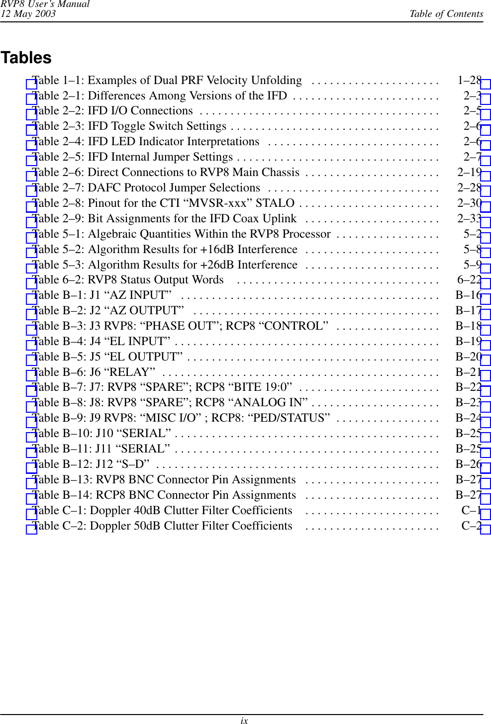
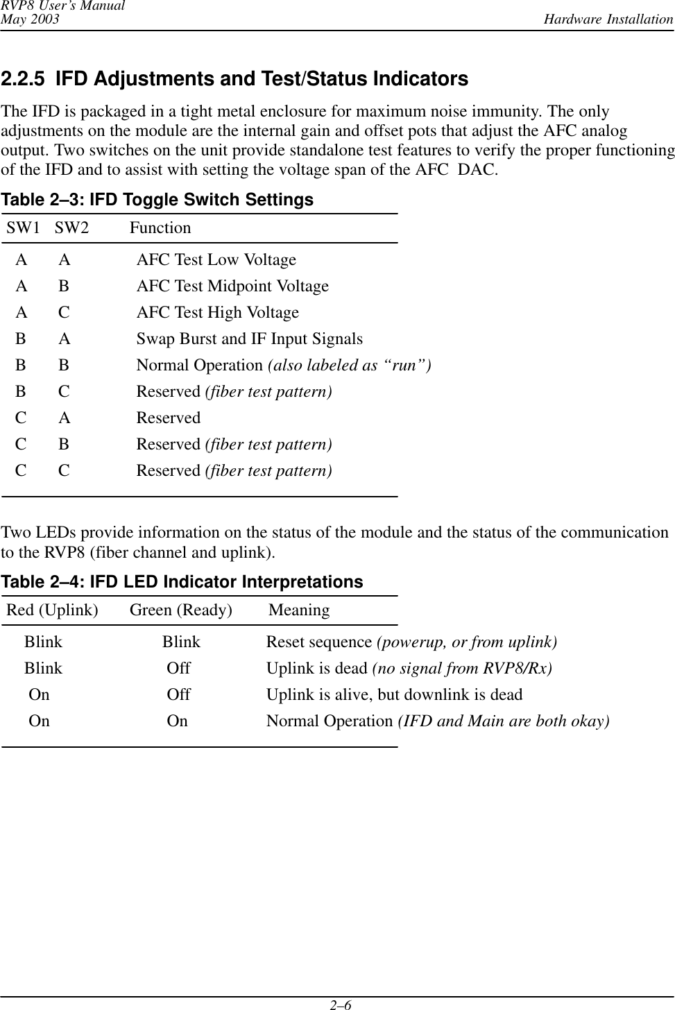
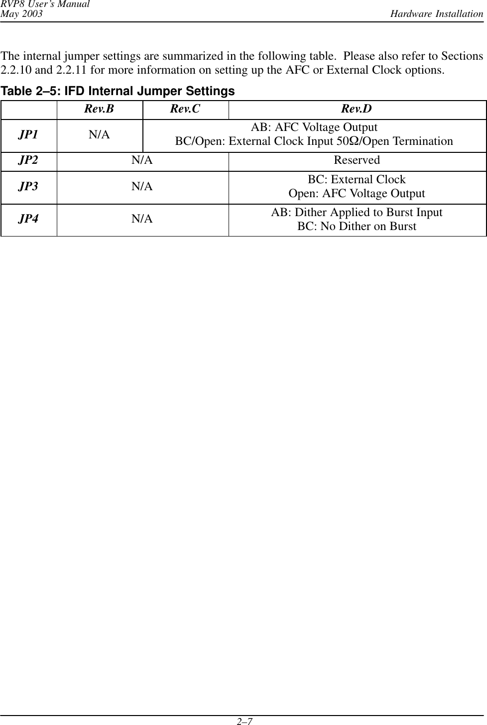
Table of ContentsRVP8 User’s Manual12 May 2003ixTablesTable 1–1: Examples of Dual PRF Velocity Unfolding 1–28 . . . . . . . . . . . . . . . . . . . . . Table 2–1: Differences Among Versions of the IFD 2–3 . . . . . . . . . . . . . . . . . . . . . . . . Table 2–2: IFD I/O Connections 2–5 . . . . . . . . . . . . . . . . . . . . . . . . . . . . . . . . . . . . . . . Table 2–3: IFD Toggle Switch Settings 2–6 . . . . . . . . . . . . . . . . . . . . . . . . . . . . . . . . . . Table 2–4: IFD LED Indicator Interpretations 2–6 . . . . . . . . . . . . . . . . . . . . . . . . . . . . Table 2–5: IFD Internal Jumper Settings 2–7 . . . . . . . . . . . . . . . . . . . . . . . . . . . . . . . . . Table 2–6: Direct Connections to RVP8 Main Chassis 2–19 . . . . . . . . . . . . . . . . . . . . . . Table 2–7: DAFC Protocol Jumper Selections 2–28 . . . . . . . . . . . . . . . . . . . . . . . . . . . . Table 2–8: Pinout for the CTI “MVSR-xxx” STALO 2–30 . . . . . . . . . . . . . . . . . . . . . . . Table 2–9: Bit Assignments for the IFD Coax Uplink 2–33 . . . . . . . . . . . . . . . . . . . . . . Table 5–1: Algebraic Quantities Within the RVP8 Processor 5–2 . . . . . . . . . . . . . . . . . Table 5–2: Algorithm Results for +16dB Interference 5–8 . . . . . . . . . . . . . . . . . . . . . . Table 5–3: Algorithm Results for +26dB Interference 5–9 . . . . . . . . . . . . . . . . . . . . . . Table 6–2: RVP8 Status Output Words   6–22 . . . . . . . . . . . . . . . . . . . . . . . . . . . . . . . . . Table B–1: J1 “AZ INPUT” B–16 . . . . . . . . . . . . . . . . . . . . . . . . . . . . . . . . . . . . . . . . . . Table B–2: J2 “AZ OUTPUT” B–17 . . . . . . . . . . . . . . . . . . . . . . . . . . . . . . . . . . . . . . . . Table B–3: J3 RVP8: “PHASE OUT”; RCP8 “CONTROL” B–18 . . . . . . . . . . . . . . . . . Table B–4: J4 “EL INPUT” B–19 . . . . . . . . . . . . . . . . . . . . . . . . . . . . . . . . . . . . . . . . . . . Table B–5: J5 “EL OUTPUT” B–20 . . . . . . . . . . . . . . . . . . . . . . . . . . . . . . . . . . . . . . . . . Table B–6: J6 “RELAY” B–21 . . . . . . . . . . . . . . . . . . . . . . . . . . . . . . . . . . . . . . . . . . . . . Table B–7: J7: RVP8 “SPARE”; RCP8 “BITE 19:0” B–22 . . . . . . . . . . . . . . . . . . . . . . . Table B–8: J8: RVP8 “SPARE”; RCP8 “ANALOG IN” B–23 . . . . . . . . . . . . . . . . . . . . . Table B–9: J9 RVP8: “MISC I/O” ; RCP8: “PED/STATUS” B–24 . . . . . . . . . . . . . . . . . Table B–10: J10 “SERIAL” B–25 . . . . . . . . . . . . . . . . . . . . . . . . . . . . . . . . . . . . . . . . . . . Table B–11: J11 “SERIAL” B–25 . . . . . . . . . . . . . . . . . . . . . . . . . . . . . . . . . . . . . . . . . . . Table B–12: J12 “S–D” B–26 . . . . . . . . . . . . . . . . . . . . . . . . . . . . . . . . . . . . . . . . . . . . . . Table B–13: RVP8 BNC Connector Pin Assignments B–27 . . . . . . . . . . . . . . . . . . . . . . Table B–14: RCP8 BNC Connector Pin Assignments B–27 . . . . . . . . . . . . . . . . . . . . . . Table C–1: Doppler 40dB Clutter Filter Coefficients   C–1 . . . . . . . . . . . . . . . . . . . . . . Table C–2: Doppler 50dB Clutter Filter Coefficients   C–2 . . . . . . . . . . . . . . . . . . . . . .
PrefaceRVP8 User’s ManualApril 2003xHardware Limited WarrantySIGMET, Inc. warrants its IRIS hardware (RVP8 and RCP8) to function according to thehardware User’s Manual documentation for a period of one year following delivery.  In the eventof a failure during the warranty period, the customer should notify SIGMET to obtain a ReturnAuthorization.  Upon receiving the Return Authorization from SIGMET, the customer ships thefailed unit to SIGMET by pre-paid freight.  SIGMET, at its option, will repair or replace thedefective unit within 30 days and return the unit to the customer.Damage caused by fire, flood, lightning, or other catastrophe, and damage caused by misuse orabuse are not covered by this warranty.In no event shall SIGMET, Inc. be liable for any direct, indirect, special, incidental, orconsequential damages arising out of the use or inability to use the hardware ordocumentation provided by SIGMET, Inc.  SIGMET, Inc. makes no warranty, eitherexpress or implied, with respect to any of the hardware or documentation, as to the quality,performance, merchantability, or fitness for a particular purpose.
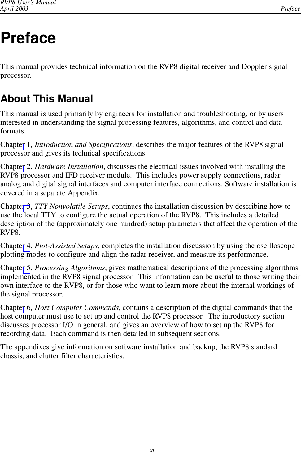
PrefaceRVP8 User’s ManualApril 2003xiPrefaceThis manual provides technical information on the RVP8 digital receiver and Doppler signalprocessor.About This ManualThis manual is used primarily by engineers for installation and troubleshooting, or by usersinterested in understanding the signal processing features, algorithms, and control and dataformats.Chapter 1, Introduction and Specifications, describes the major features of the RVP8 signalprocessor and gives its technical specifications.Chapter 2, Hardware Installation, discusses the electrical issues involved with installing theRVP8 processor and IFD receiver module.  This includes power supply connections, radaranalog and digital signal interfaces and computer interface connections. Software installation iscovered in a separate Appendix.Chapter 3, TTY Nonvolatile Setups, continues the installation discussion by describing how touse the local TTY to configure the actual operation of the RVP8.  This includes a detaileddescription of the (approximately one hundred) setup parameters that affect the operation of theRVP8.Chapter 4, Plot-Assisted Setups, completes the installation discussion by using the oscilloscopeplotting modes to configure and align the radar receiver, and measure its performance.Chapter 5, Processing Algorithms, gives mathematical descriptions of the processing algorithmsimplemented in the RVP8 signal processor.  This information can be useful to those writing theirown interface to the RVP8, or for those who want to learn more about the internal workings ofthe signal processor.Chapter 6, Host Computer Commands, contains a description of the digital commands that thehost computer must use to set up and control the RVP8 processor.  The introductory sectiondiscusses processor I/O in general, and gives an overview of how to set up the RVP8 forrecording data.  Each command is then detailed in subsequent sections.The appendixes give information on software installation and backup, the RVP8 standardchassis, and clutter filter characteristics.
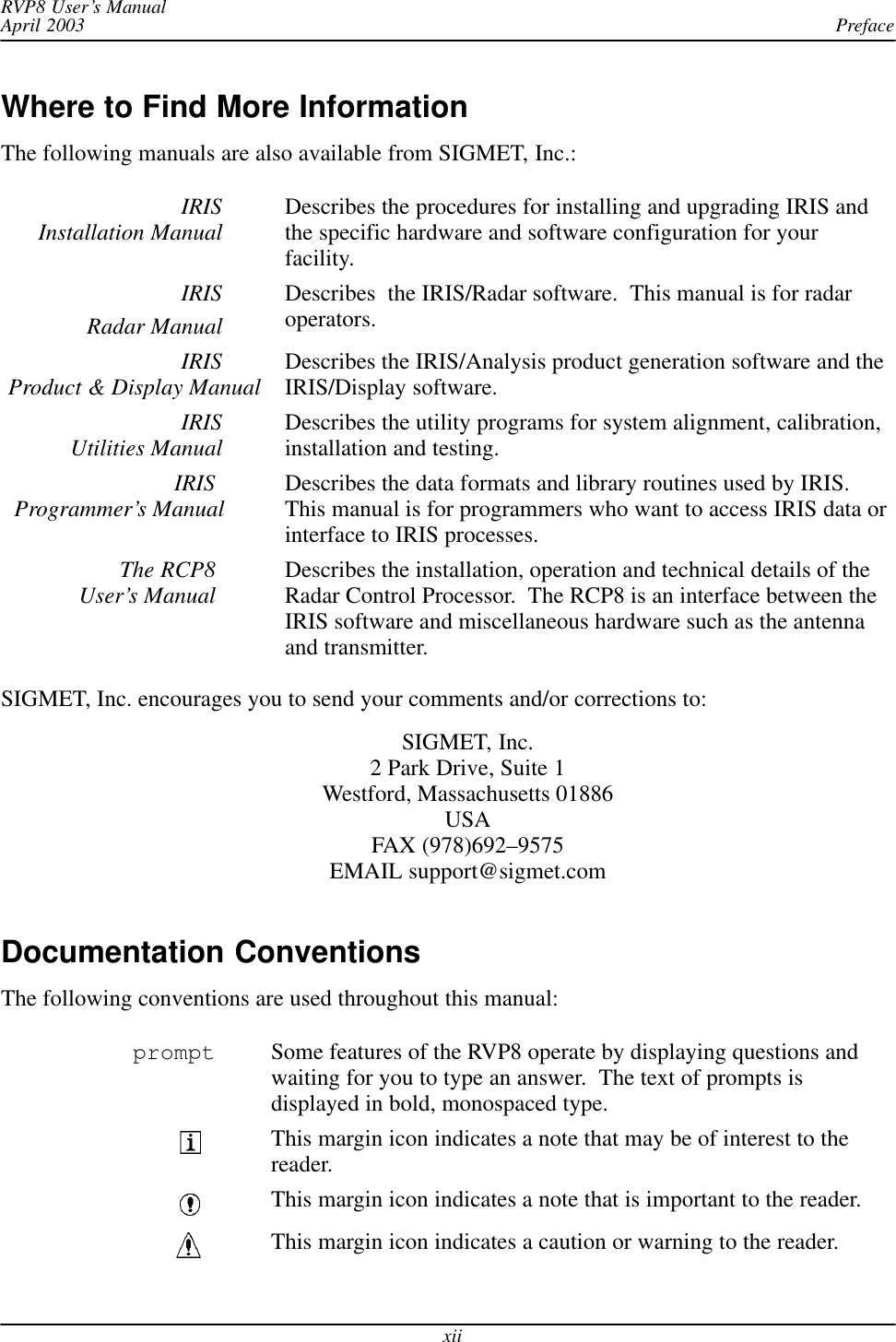
PrefaceRVP8 User’s ManualApril 2003xiiWhere to Find More InformationThe following manuals are also available from SIGMET, Inc.:IRISInstallation Manual Describes the procedures for installing and upgrading IRIS andthe specific hardware and software configuration for yourfacility.IRISRadar ManualDescribes  the IRIS/Radar software.  This manual is for radaroperators.IRISProduct & Display Manual Describes the IRIS/Analysis product generation software and theIRIS/Display software.IRISUtilities Manual Describes the utility programs for system alignment, calibration,installation and testing.IRIS Programmer’s Manual Describes the data formats and library routines used by IRIS.This manual is for programmers who want to access IRIS data orinterface to IRIS processes.The RCP8 User’s Manual Describes the installation, operation and technical details of theRadar Control Processor.  The RCP8 is an interface between theIRIS software and miscellaneous hardware such as the antennaand transmitter.SIGMET, Inc. encourages you to send your comments and/or corrections to:SIGMET, Inc.2 Park Drive, Suite 1Westford, Massachusetts 01886USAFAX (978)692–9575EMAIL support@sigmet.comDocumentation ConventionsThe following conventions are used throughout this manual:prompt Some features of the RVP8 operate by displaying questions andwaiting for you to type an answer.  The text of prompts isdisplayed in bold, monospaced type.This margin icon indicates a note that may be of interest to thereader.This margin icon indicates a note that is important to the reader.This margin icon indicates a caution or warning to the reader.
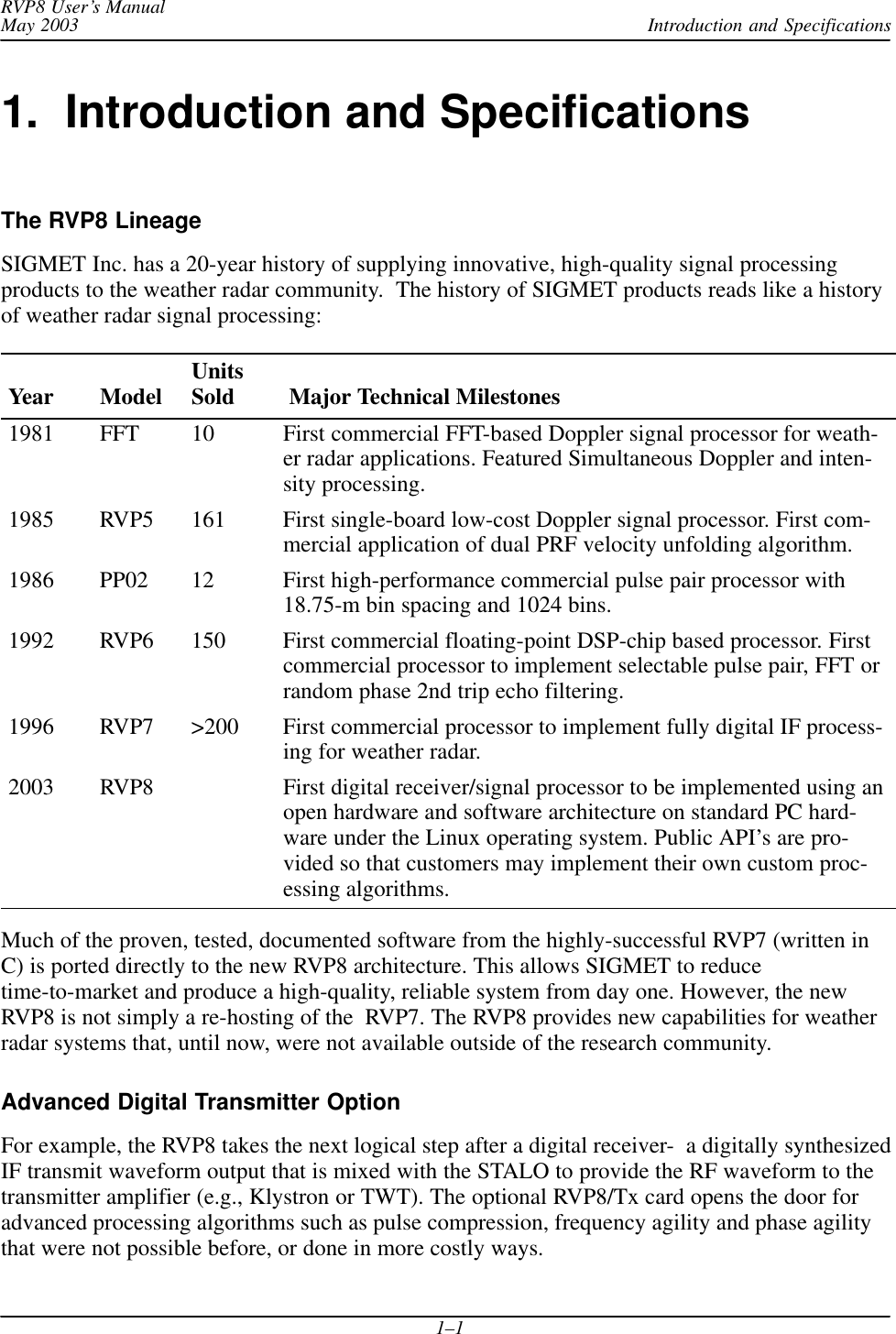
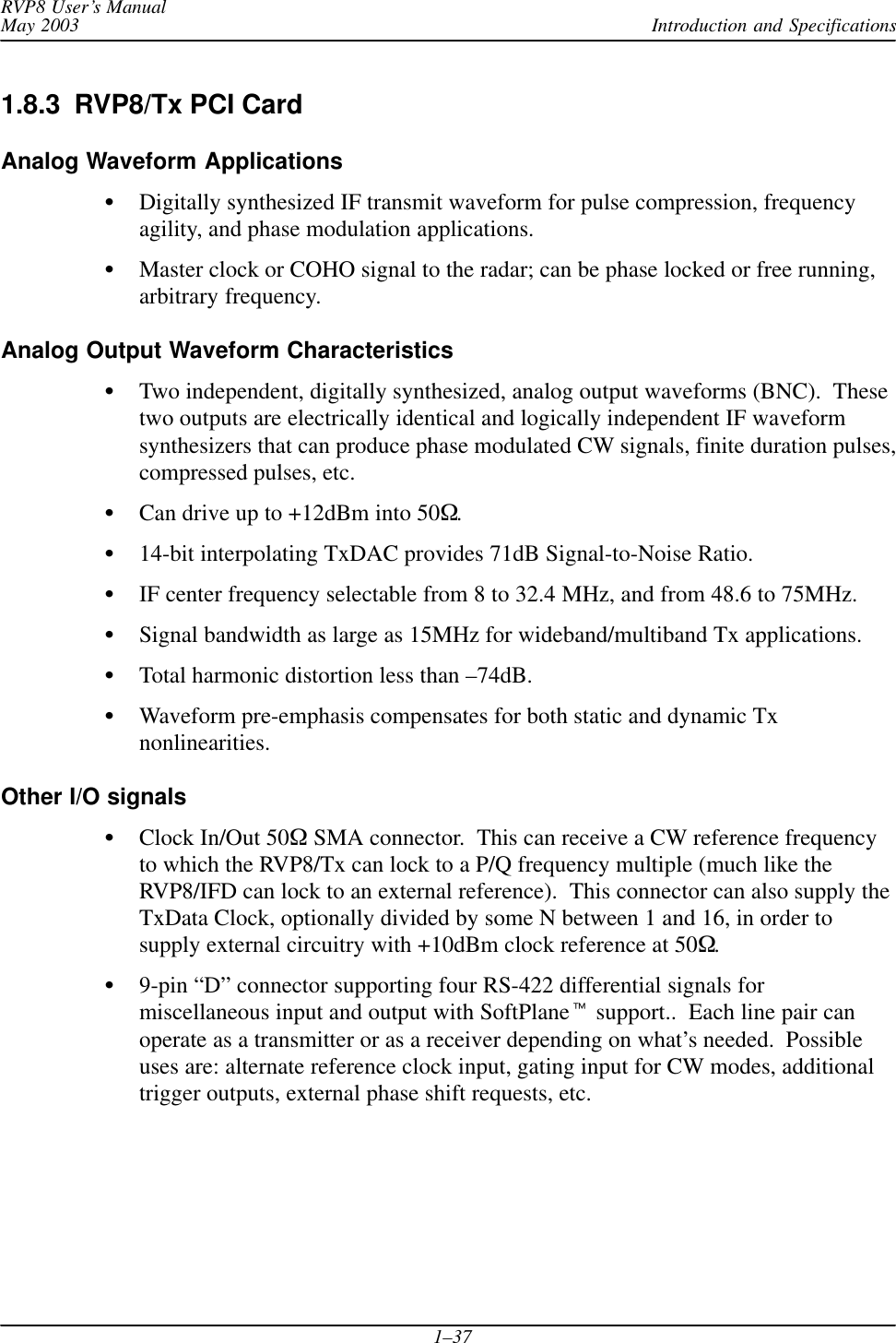
Introduction and SpecificationsRVP8 User’s ManualMay 20031–11.  Introduction and SpecificationsThe RVP8 LineageSIGMET Inc. has a 20-year history of supplying innovative, high-quality signal processingproducts to the weather radar community.  The history of SIGMET products reads like a historyof weather radar signal processing:Year Model UnitsSold  Major Technical Milestones1981 FFT 10 First commercial FFT-based Doppler signal processor for weath-er radar applications. Featured Simultaneous Doppler and inten-sity processing.1985 RVP5 161 First single-board low-cost Doppler signal processor. First com-mercial application of dual PRF velocity unfolding algorithm.1986 PP02 12 First high-performance commercial pulse pair processor with18.75-m bin spacing and 1024 bins.1992 RVP6 150 First commercial floating-point DSP-chip based processor. Firstcommercial processor to implement selectable pulse pair, FFT orrandom phase 2nd trip echo filtering.1996 RVP7 >200 First commercial processor to implement fully digital IF process-ing for weather radar.2003 RVP8 First digital receiver/signal processor to be implemented using anopen hardware and software architecture on standard PC hard-ware under the Linux operating system. Public API’s are pro-vided so that customers may implement their own custom proc-essing algorithms.Much of the proven, tested, documented software from the highly-successful RVP7 (written inC) is ported directly to the new RVP8 architecture. This allows SIGMET to reducetime-to-market and produce a high-quality, reliable system from day one. However, the newRVP8 is not simply a re-hosting of the  RVP7. The RVP8 provides new capabilities for weatherradar systems that, until now, were not available outside of the research community.Advanced Digital Transmitter OptionFor example, the RVP8 takes the next logical step after a digital receiver-  a digitally synthesizedIF transmit waveform output that is mixed with the STALO to provide the RF waveform to thetransmitter amplifier (e.g., Klystron or TWT). The optional RVP8/Tx card opens the door foradvanced processing algorithms such as pulse compression, frequency agility and phase agilitythat were not possible before, or done in more costly ways.
Introduction and SpecificationsRVP8 User’s ManualMay 20031–2Open Hardware and Software DesignCompared to previous processors that were built around proprietary DSP chips, perhaps the mostinnovative aspect of the RVP8 is that it is implemented on standard PC hardware and softwarethat can be purchased from a wide variety of sources. The Intel Pentium/PCI approach promisescontinued improvement in processor speed, bus bandwidth and the availability of low–costcompatible hardware and peripherals. The performance of an entry level RVP8 (currently dual2.4 GHz Pentium processors) is 6 times faster than the fastest RVP7 ever produced (with twoRVP7/AUX boards).Aside from the open hardware approach, the RVP8 has an open software approach as well. TheRVP8 runs in the context of the Linux operating system. The code is structured and public API’sare provided so that research customers can modify/replace existing SIGMET algorithms, orwrite their own software from scratch using the RVP8 software structure as a foundation onwhich to build.The advantage of the open hardware and software PCI approach is reduced cost and the abilityfor customers to maintain, upgrade and expand the processor in the future by purchasingstandard, low cost PC components from local sources.SoftPlane  High–Speed I/O InterconnectThere are potentially many different I/O signals emanating from the backpanel of the RVP8.Most of these conform to well-known electrical and protocol standards (VGA, SCSI, 10–BaseT,RS-232 Serial, PS/2 Keyboard, etc.), and can be driven by standard commercial boards that areavailable from multiple vendors. However, there are other interface signals such as triggers andclocks that require careful timing. These precise signals cannot tolerate the PCI bus latency. Forsignals that  have medium–speed requirements (~1 microsec latency) for which the PCI bus isinappropriate; and others that require a high–speed (~ 1 ns latency) connection that can only beachieved with a dedicated wire, the RVP8 Softplane  provides the solution.Physically, the Softplane is a 16-wire digital “daisy-chain” bus that plugs into the tops of theRVP8/Rx, RVP8/Tx, and I/O boards. The wires connect to the FPGA chips on each card, and thefunction of each wire is assigned at run–time based on the connectivity needs of the overallsystem. The Softplane allocates a dedicated wire to carry each high-speed signal; but groups ofmedium-speed signals are multiplexed onto single wires in order to conserve resources. Eventhough there are only 16 wires available, the Softplane is able to carry several high-speed signalsand hundreds of medium–speed signals, as long as the total bandwidth does not exceed about600MBits/sec.The Softplane I/O is configured at run–time based on a file description rather than customwiring such as wirewrap. Neither the PCI backplane nor the physical Softplane are customizedin any way. Since there is no custom wiring, a failed board can be replaced with a genericoff–the–shelf spare, and that spare will automatically resume whatever functions had beenassigned to the original board. Similarly, if the chassis itself were to fail, then simply pluggingthe boards into another generic chassis would restore complete operation. Cards and chassis canbe swapped between systems without needing to worry about custom wiring.
Introduction and SpecificationsRVP8 User’s ManualMay 20031–3Standard LAN Interconnection for Data Transfer or Parallel ProcessingFor communication with the outside world, the RVP8 supports as standard a 10/100/1000 Base TEthernet. For most applications, the 100 BaseT Ethernet is used to transfer moment results (Z, T,V, W) to the applications host computer (e.g., a product generator). However, the gigabitEthernet is sufficiently fast to allow UDP broadcast of the I and Q values for the purpose ofarchiving and/or parallel processing. In other words, a completely separate signal processor caningest and process the I and Q values generated by the RVP8.
Introduction and SpecificationsRVP8 User’s ManualMay 20031–41.1  System Configuration ConceptsThe hardware building blocks of an RVP8 system are actually quite few in number:RVP8/IFD  IF Digitizer Unit- This is a separate sealed unit usually mounted inthe receiver cabinet. The primary input to the IFD is the received IF signal. Inaddition, the IFD has channels to sample the transmit pulse and to take in anexternal clock to phase lock the A/D conversion with the transmit pulse (not usedfor magnetron systems).RVP8/Rx  Card- A PCI long format card mounted in the chassis. It connects tothe IFD by a fiberoptic downlink and a coax uplink which can be up to 100mdistant. In addition, there are two BNC trigger input/output (programmable).I/O-62  Card and Connector Panel- These handle all of the various I/Oassociated with a radar signal processor, such as triggers, antenna angles,polarization switch controls, pulse width control, etc. The Connector Panel ismounted on either the front or rear of the equipment rack and a cable (supplied)connects the panel to the I/O-62.Optional RVP8/Tx  card- This supplies two IF output signals withprogrammable frequency, phase and amplitude modulation. In the simplest case,it supplies the COHO which is then mixed up with the STALO to generate thetransmit RF for Klystron or TWT systems. This card is not necessary formagnetron systems.PC Chassis and Processor with various peripherals- a robust 6U rack mountunit with either a mother board or single board computer (SBC) in a passive backplane. There is a diagnostic front panel display, disk (mechanical or flash),CDRW, keyboard, mouse and optional monitor for local diagnostic work. Dual ortri–redundant power supplies are used and there are redundant fans as well.This modular hardware approach allows the various components to be mixed and matched tosupport applications ranging from a simple magnetron system to an advanced dual polarizationsystem with pulse compression.  Typically SIGMET supplies turn-key systems, although someOEM customers who produce many systems purchase individual components and integrate themby themselves. This allows OEM customers to put their own custom “stamp” on the processorand even their own custom software if they so choose.For the turnkey systems provided by SIGMET, the basic chassis is a 6U rackmount unit asdescribed above. A 2U chassis can be provided for applications for which space is limited. Avery low cost approach is to use a desk side PC, but this is not recommended for applicationsthat require long periods of unattended operation.To illustrate various RVP8 configurations, some typical examples are shown below. For clarity,all the examples show the single–board computer approach. A mother board approach isequivalent.
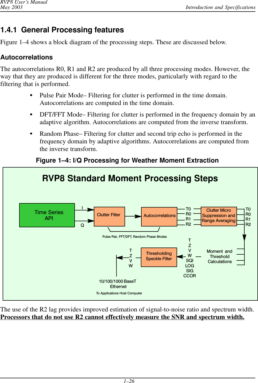
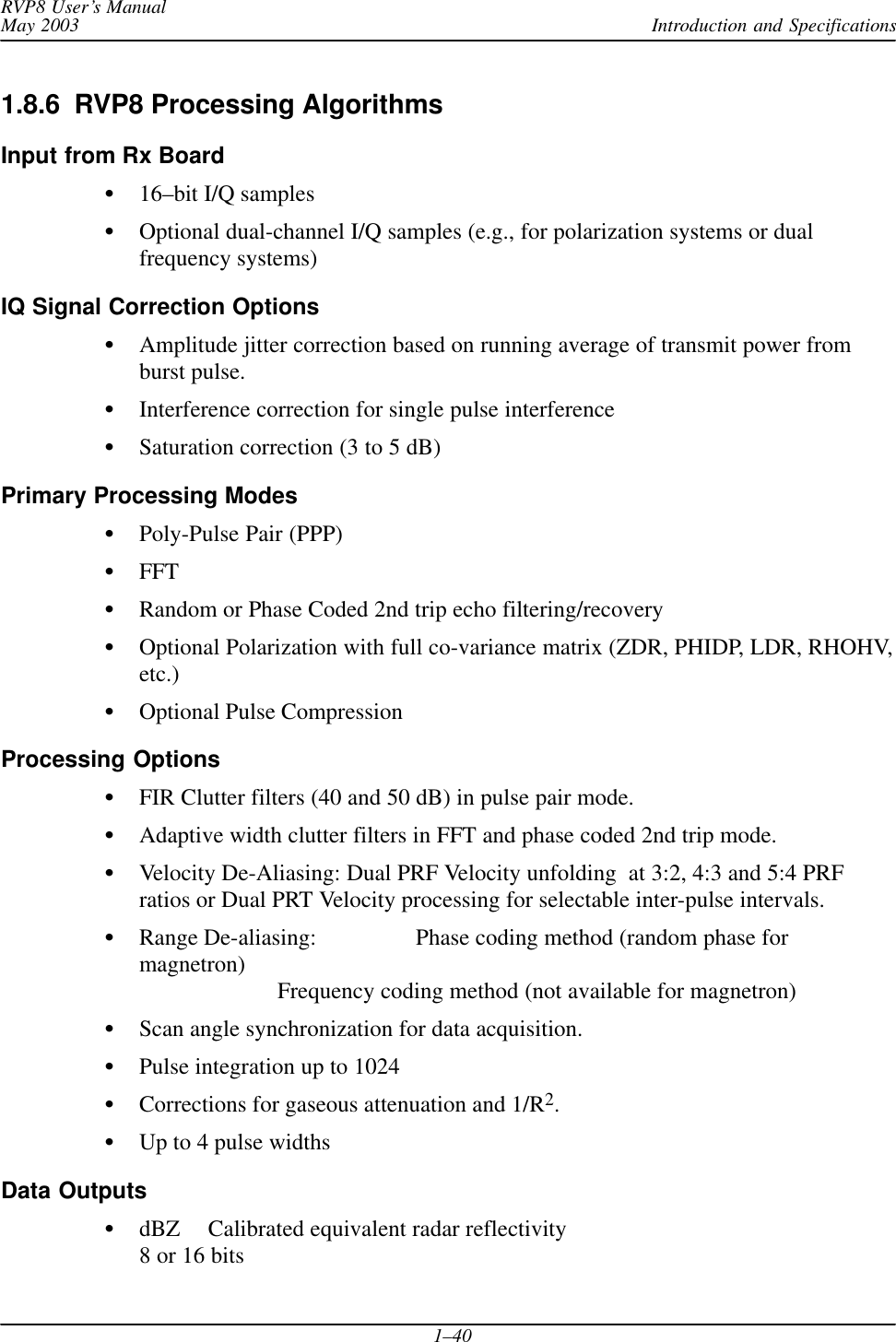
Introduction and SpecificationsRVP8 User’s ManualMay 20031–5KeyboardMouseMonitor10/100 BaseT LAN InterfaceIFD Fiber DownlinkCOAX UplinkRS232C Antenna AnglesRVP8 Configuration Example: Basic Magnetron SystemTriggersIF SignalIF Magnetron BurstDAFCDigital STALOOptionalUtilities14-BitSBCRVP8/RxExample 1: Basic Magnetron SystemThe building blocks required to construct the basic system are:IFD- IF Digitizer installed in the radar receiver cabinet. This can be located up to 100meters from the RVP8 main chassis (fiber optic connection). The DAFC (Digital AFC) isan option to interface to a digitally controlled STALO. Like the RVP7, the RVP8provides full AFC with burst pulse auto-tracking.RVP8/Rx- The digital receiver collects digitized samples from the IFD and does theprocessing to obtain  I/Q. It also provides two trigger connections configurable for inputor output.SBC Card- Single Board Computer with dual SMP processors  (PC) running Linux.The figure above shows a basic magnetron system constructed with an IFD, and two PCI cards.A standard RS-232 serial input (included with the SBC) is used for obtaining the antenna anglesand the output/input trigger is provided directly from the Rx card. This system has 5 times theprocessing power of the fastest version of the previous generation processor (RVP7/Main boardplus 2 RVP7/AUX boards) so that it is capable of performing DFT processing in 2048 rangebinswith advanced algorithms such as random phase 2nd trip echo filtering and recovery.
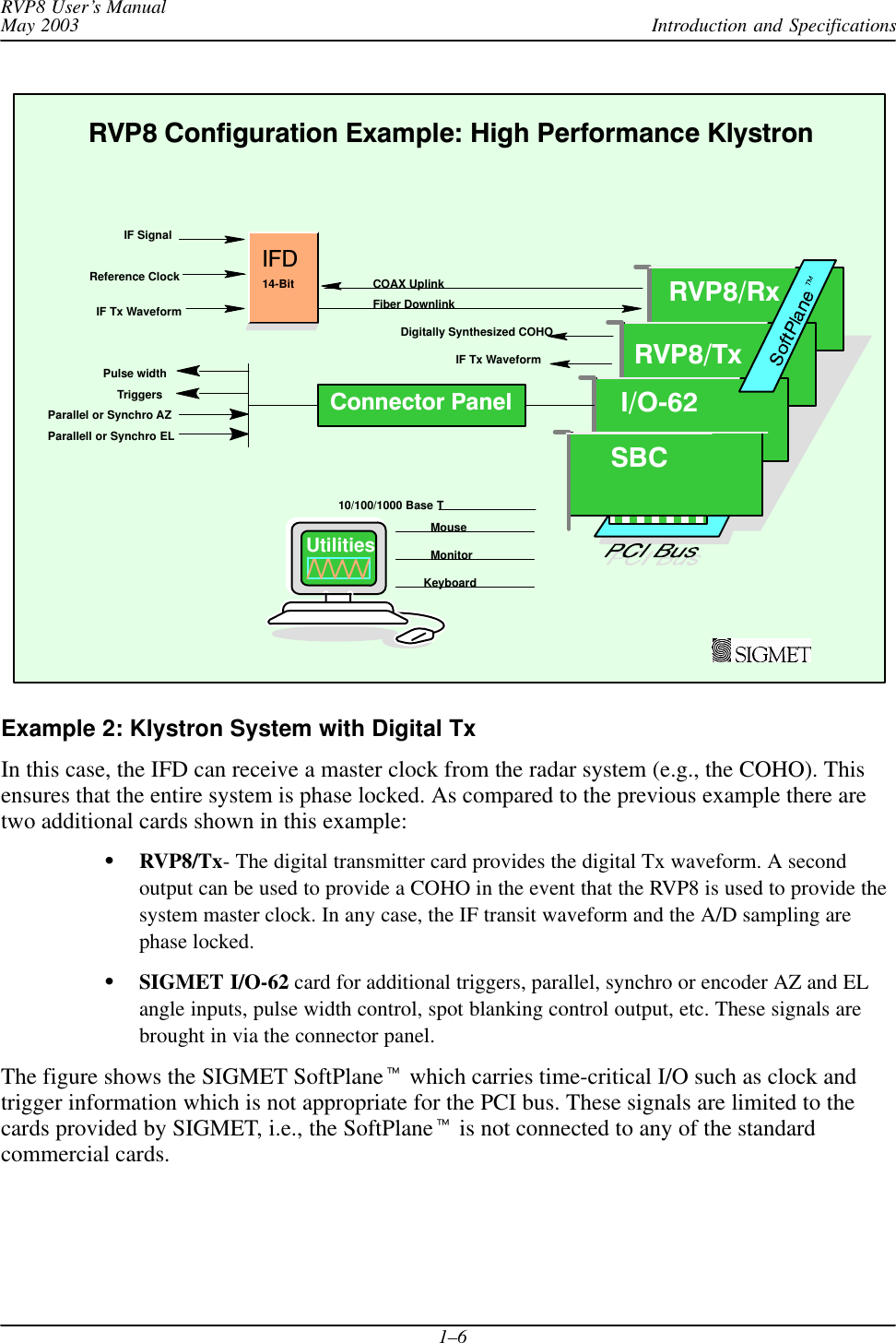
Introduction and SpecificationsRVP8 User’s ManualMay 20031–6RVP8 Configuration Example: High Performance KlystronKeyboardMouseMonitor10/100/1000 Base TIFDFiber DownlinkCOAX UplinkTriggersIF SignalReference ClockDigitally Synthesized COHOParallel or Synchro AZParallell or Synchro ELPulse width IF Tx WaveformUtilitiesIF Tx Waveform14-BitI/O62SBCRVP8/TxRVP8/RxConnector PanelExample 2: Klystron System with Digital TxIn this case, the IFD can receive a master clock from the radar system (e.g., the COHO). Thisensures that the entire system is phase locked. As compared to the previous example there aretwo additional cards shown in this example:RVP8/Tx- The digital transmitter card provides the digital Tx waveform. A secondoutput can be used to provide a COHO in the event that the RVP8 is used to provide thesystem master clock. In any case, the IF transit waveform and the A/D sampling arephase locked.SIGMET I/O-62 card for additional triggers, parallel, synchro or encoder AZ and ELangle inputs, pulse width control, spot blanking control output, etc. These signals arebrought in via the connector panel.The figure shows the SIGMET SoftPlane which carries time-critical I/O such as clock andtrigger information which is not appropriate for the PCI bus. These signals are limited to thecards provided by SIGMET, i.e., the SoftPlane is not connected to any of the standardcommercial cards.
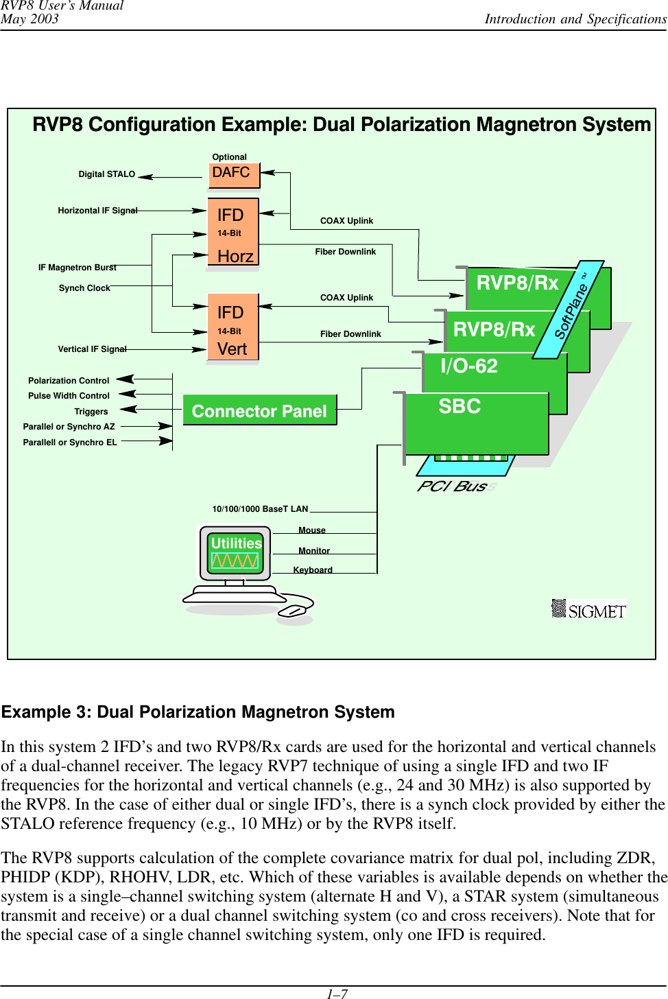
Introduction and SpecificationsRVP8 User’s ManualMay 20031–7IFDFiber DownlinkCOAX UplinkRVP8 Configuration Example: Dual Polarization Magnetron SystemKeyboardMouseMonitor10/100/1000 BaseT LANIFDHorizontal IF SignalDAFCDigital STALOOptionalVertical IF SignalUtilities14-Bit14-BitIF Magnetron BurstSynch ClockFiber DownlinkHorzVert I/O62SBCRVP8/RxRVP8/RxCOAX UplinkTriggersParallel or Synchro AZParallell or Synchro ELPulse Width ControlConnector PanelPolarization ControlExample 3: Dual Polarization Magnetron SystemIn this system 2 IFD’s and two RVP8/Rx cards are used for the horizontal and vertical channelsof a dual-channel receiver. The legacy RVP7 technique of using a single IFD and two IFfrequencies for the horizontal and vertical channels (e.g., 24 and 30 MHz) is also supported bythe RVP8. In the case of either dual or single IFD’s, there is a synch clock provided by either theSTALO reference frequency (e.g., 10 MHz) or by the RVP8 itself.The RVP8 supports calculation of the complete covariance matrix for dual pol, including ZDR,PHIDP (KDP), RHOHV, LDR, etc. Which of these variables is available depends on whether thesystem is a single–channel switching system (alternate H and V), a STAR system (simultaneoustransmit and receive) or a dual channel switching system (co and cross receivers). Note that forthe special case of a single channel switching system, only one IFD is required.
Introduction and SpecificationsRVP8 User’s ManualMay 20031–8COTS AccessoriesAside from the basic PCI cards required for the radar application, there are additional cards thatcan be installed to meet different customer requirements, e.g.,10/100–BaseT Ethernet card for additional network I/O (e.g., a backup network).RS-232/RS-422 serial cards for serial angles, remote TTY control, etc.Sound card to synthesize audio waveforms for wind profiler applications.GPS card for time synch.IEEE 488 GPIB card for control of test equipment.The bottom line is that the PCI open hardware approach provides unparalleled hardwareflexibility. In addition, the availability of compatible low-cost replacement or upgrade parts isassured for years into the future.
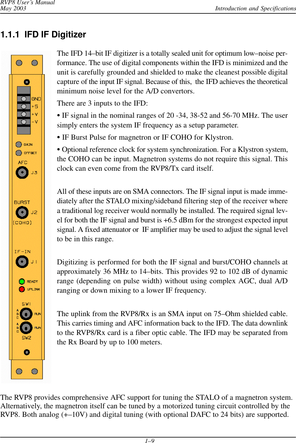
Introduction and SpecificationsRVP8 User’s ManualMay 20031–91.1.1  IFD IF DigitizerThe IFD 14–bit IF digitizer is a totally sealed unit for optimum low–noise per-formance. The use of digital components within the IFD is minimized and theunit is carefully grounded and shielded to make the cleanest possible digitalcapture of the input IF signal. Because of this,  the IFD achieves the theoreticalminimum noise level for the A/D convertors.There are 3 inputs to the IFD: IF signal in the nominal ranges of 20 -34, 38-52 and 56-70 MHz. The usersimply enters the system IF frequency as a setup parameter. IF Burst Pulse for magnetron or IF COHO for Klystron. Optional reference clock for system synchronization. For a Klystron system,the COHO can be input. Magnetron systems do not require this signal. Thisclock can even come from the RVP8/Tx card itself.All of these inputs are on SMA connectors. The IF signal input is made imme-diately after the STALO mixing/sideband filtering step of the receiver wherea traditional log receiver would normally be installed. The required signal lev-el for both the IF signal and burst is +6.5 dBm for the strongest expected inputsignal. A fixed attenuator or  IF amplifier may be used to adjust the signal levelto be in this range.Digitizing is performed for both the IF signal and burst/COHO channels atapproximately 36 MHz to 14–bits. This provides 92 to 102 dB of dynamicrange (depending on pulse width) without using complex AGC, dual A/Dranging or down mixing to a lower IF frequency.The uplink from the RVP8/Rx is an SMA input on 75–Ohm shielded cable.This carries timing and AFC information back to the IFD. The data downlinkto the RVP8/Rx card is a fiber optic cable. The IFD may be separated fromthe Rx Board by up to 100 meters.The RVP8 provides comprehensive AFC support for tuning the STALO of a magnetron system.Alternatively, the magnetron itself can be tuned by a motorized tuning circuit controlled by theRVP8. Both analog (+–10V) and digital tuning (with optional DAFC to 24 bits) are supported.
Introduction and SpecificationsRVP8 User’s ManualMay 20031–101.1.2  Digital Receiver PCI Card (RVP8/Rx)The RVP8/Rx card receives the digitized IF samples from the IFD via the fiber opticlink. The advantage of this design is that the receiver electronics (LNA, RF mixer,IF preamp, and IFD) can be located as far as 100–meters away from the RVP8 mainchassis. This makes it possible to choose optimum locations for both the IFD and theRVP8, e.g., the IFD could be mounted on the antenna itself, and the processor boxin a nearby equipment room.The RVP8/Rx is 100% compatible with the 14–bit RVP7/IFD, but it also includeshooks for future IFD’s operating at higher sampling clock rates. Two additional BNCconnectors are included on the board’s faceplate. These can be used for trigger input,programmable trigger output, or a simple LOG analog ascope waveform.A remarkable amount of computing power is resident on the receiver board, in theform of an FIR filter array that can execute 6.9 billion multiply/accumulate cyclesper second. These chips serve as the first stage of processing of the raw IF data sam-ples. Their job is to perform the down–conversion, bandpass, and deconvolutionsteps that are required to produce (I,Q) time series. The time series data are then trans-ferred over the PCI bus to the SBC for final processing.The FIR filter array can buffer as much as 80 microsec of 36MHz IF samples, and then computea pair of 2880–point dot products on those data every 0.83 microsec. This could be used toproduce over-sampled (I,Q) time series having a range resolution of 125–meters and abandwidth as narrow as 30Khz. The same computation could also yield independent 125–metertime series data from an 80 microsec compressed pulse whose transmit bandwidth wasapproximately 1MHz.Finer range resolutions are also possible, down to a minimum of 25–meters. A special feature ofthe RVP8/Rx is that the bin spacing of the (I,Q) data can be set to any desired value between 25and 2000 meters. Range bins are placed accurately to within +2.2 meters of any selected grid,which does not have to be an integer multiple of the sampling clock. However, when an integermultiple (N x 8.333–meters) is selected, the error in bin placement effectively drops to zero.Dual polarization radars that are capable of simultaneous reception for both horizontal andvertical channels can be interfaced to the RVP8 using a separate RVP8/Rx and IFD for eachchannel. Note that the multiplexed dual IF approach used for the RVP7 with a single IFD canalso be used.One of the primary advantages of the digital receiver approach is that wide linear dynamic rangecan be achieved without the need for complex AGC circuits that require both phase andamplitude calibration.
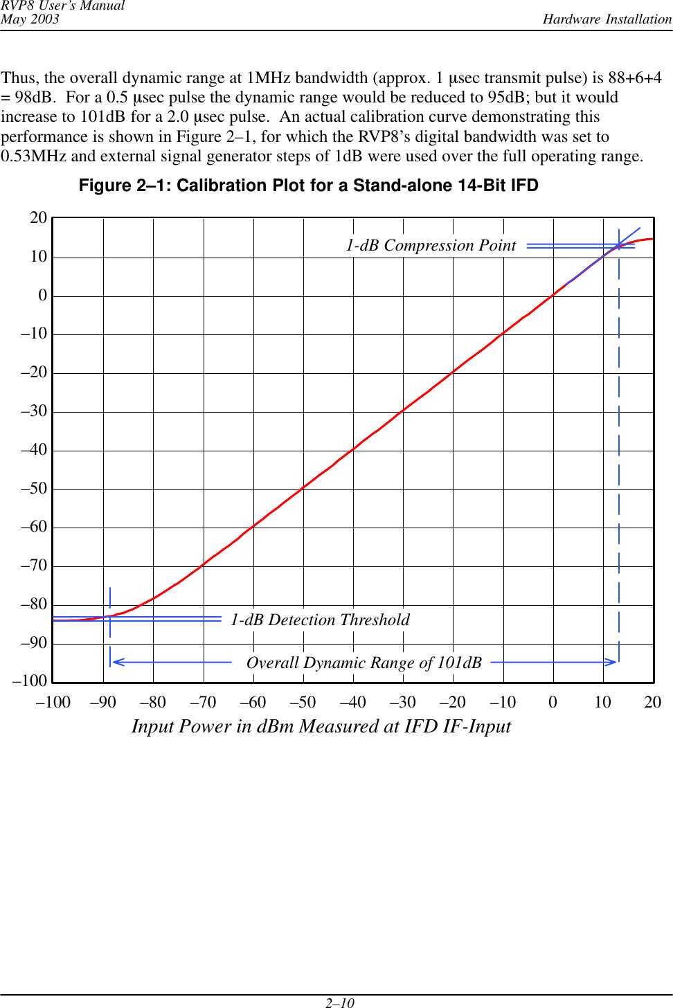
Introduction and SpecificationsRVP8 User’s ManualMay 20031–11Calibration Plot for RVP8/IFDThe figure above shows a calibration plot for a 14–bit IFD with the digital filter matched to a 2microsecond pulse. The performance in this case is >100 dB dynamic range– fully linear.The RVP8 performs several real time signal corrections to the I/Q samples from the Rx,including:Amplitude Correction- A running average of the transmit pulse power  in the magnetron burstchannel is computed in real-time by the RVP8/Rx. The individual received I/Q samples arecorrected for pulse–to–pulse deviations from this average. This can substantially improve the“phase stability” of a magnetron system to improve the clutter cancelation performance to nearKlystron levels.Phase Correction- The phase of the transmit waveform is measured for each pulse (either theburst pulse for magnetron systems or the Tx Waveform for coherent systems).  The I/Q valuesare adjusted for the actual measured phase. The coherency achievable is better than 0.1 degreesby this technique.Large Signal Linearization- When an IF signal saturates, there is still considerable informationin the signal since only the peaks are clipped. The proprietary large signal linearizationalgorithm used in the RVP8 provides an extra 3 to 4 dB of dynamic range by accounting for theeffects of saturation.The RVP8/Rx card provides the same comprehensive configuration and test utilities as theRVP7, with the difference that no external host computer is required to run the utilities. Theseutilities can be run either locally or remotely– over the network! Some examples are shownbelow:
Introduction and SpecificationsRVP8 User’s ManualMay 20031–12Digital IF Band Pass Design ToolThe built–in filter design tool makes it easy foranyone to design the optimal IF filter to matcheach pulse width and application. Simply specifythe impulse response and pass band and the filterappears. The user interface makes it easy to wid-en/narrow the filter with simple keyboard com-mands. There is even a command to automatical-ly search for an optimal filter. This display can also show the actual spectrumof the transmit burst pulse for quality control andcomparison with the filter.Burst Pulse Alignment ToolThe quality assessment of the transmit burstpulse and its precise alignment at range zeroare easy to do, either manually using this tooland/or automatically using the burst pulseauto-track feature. This performs a 2D searchin both time and frequency space if a validburst pulse is not detected. The automatictracking makes the AFC robust to start–uptemperature changes and pulse width changesthat can effect the magnetron frequency.AFC alignment/check is now much easiersince it can be done manually from a centralmaintenance site or fully automatically.Received Signal Spectrum Analysis ToolThe RVP8 provides plots of the IF signal versusrange as well as spectrum analysis of the signalas shown in this example.In the past, these types of displays and tools re-quired that a highly-skilled engineer transportsome very  expensive test equipment to the radarsite. Now, detailed analysis and configurationcan all be done from a central maintenance facil-ity via the network. For a multi-radar networkthis results in substantial savings in equipment,time and labor.
Introduction and SpecificationsRVP8 User’s ManualMay 20031–131.1.3  Mother Board or Single-Board Computer (SBC)The dual-CPU Pentium mother board or single-board computer (SBC) acts as the hostto the Linux operating system and provides all of the compute resources for processingthe I/Q values that are generated by the RVP8/Rx card. Standard keyboard, mouse andmonitor connections are on the Rx backpanel, along with a 10/100/1000 BaseT Ether-net port. The system does not require that a keyboard, mouse or monitor be connectedwhich is typically the case at an unattended site. An SBC example is shown on the left.Motherboards and SBC’s are available from many vendors, at various speeds  Typical-ly the SBC is equipped with 128 MB RAM. The RVP8 chassis has a front bay for eithera >20 GB hard disk or a Flash Disk. The Flash Disk approach is well suited to applica-tions where high–reliability is important. CDRW is also provided for software mainte-nance. Note that the latest versions of the RVP8 software and documentation can al-ways be down-loaded from SIGMET’s web site for FREE.The SBC also plays host for SIGMET’s RVP8 Utilities which provide test, configura-tion, control and monitoring software as well as built–in on-line documentation.1.1.4  Digital Transmitter PCI Card (RVP8/Tx) Many of the exciting new meteorological applications for the RVP8 are made possibleby its ability to function as a digital radar transmitter. The RVP8/Tx PCI card synthe-sizes an output waveform that is centered at at the radar’s intermediate frequency. Thissignal is filtered using analog components, then up–converted to RF, and finally am-plified for transmission. The actual transmitter can be a solid state or vacuum tube de-vice. The RVP8 can even correct for waveform distortion by adaptively “pre–distort-ing” the transmit waveform, based on the measured transmit burst sample.The Tx card has a BNC output for the IF Tx waveform. In addition, there is a secondoutput for an auxiliary signal or clock, or for a clock input. At the bottom of the cardis a 9–pin connector for arbitrary I/O (e.g., TTL, RS422, additional clock).The RVP8 digital transmitter finds a place within the overall radar system that exactlycomplements the digital receiver. The receiver samples an IF waveform that has beendown–converted from RF, and the transmitter synthesizes an IF waveform for up–con-version to RF. The beauty of this approach is that the RVP8 now has complete controlover both halves of the radar, making possible a whole new realm of matched Tx/Rxprocessing algorithms. Some examples are given below:Phase Modulation- Some radar processing algorithms rely on modulating the phase ofthe transmitter from pulse to pulse. This is traditionally done using an external IF phasemodulator that is operated by digital control lines. While this usually works well, itrequires additional hardware and cabling within the radar cabinet, and the
Introduction and SpecificationsRVP8 User’s ManualMay 20031–14phase/amplitude characteristics may not be precise or repeatable. In contrast, theRVP8/Tx can perform precise phase modulation to any desired angle, without requiringthe use of external phase shifting hardware.Pulse Compression- There is increasing demand for siting radars in urban areasthat also happen to have strict regulations on transmit emissions. Often the peaktransmit power is limited in these areas; so the job for the weather radar is tosomehow illuminate its targets using longer pulses at lower power. The problem,of course, is that a simple long pulse lacks the ability (bandwidth) to discerntargets in range. The remedy is to increase the Tx bandwidth by modulating theoverall pulse envelope, so that a reasonable range resolution is restored. Theexceptional fidelity of the RVP8/Tx waveform can accomplish this withoutintroducing any of the spurious modulation components that often occur whenexternal phase modulation hardware is used.Frequency Agility- This has been well studied within the research community,but has remained out of the reach of practical weather radars. The RVP8/Txchanges all of this, because frequency agility is as simple as changing the centerfrequency of the synthesized IF waveform. Many new Range/Doppler unfoldingalgorithms become possible when multiple transmit frequencies can coexist.Frequency agility can also be combined with pulse compression to remedy theblind spot at close ranges while the long pulse is being transmitted.COHO synthesis-  The RVP8/Tx output waveform can be programmed to be asimple CW sine wave. It can be synthesized at any desired frequency andamplitude, and its phase is locked to the other system clocks. If you need adedicated oscillator at some random frequency in the IF band, this is a simpleway to get it.
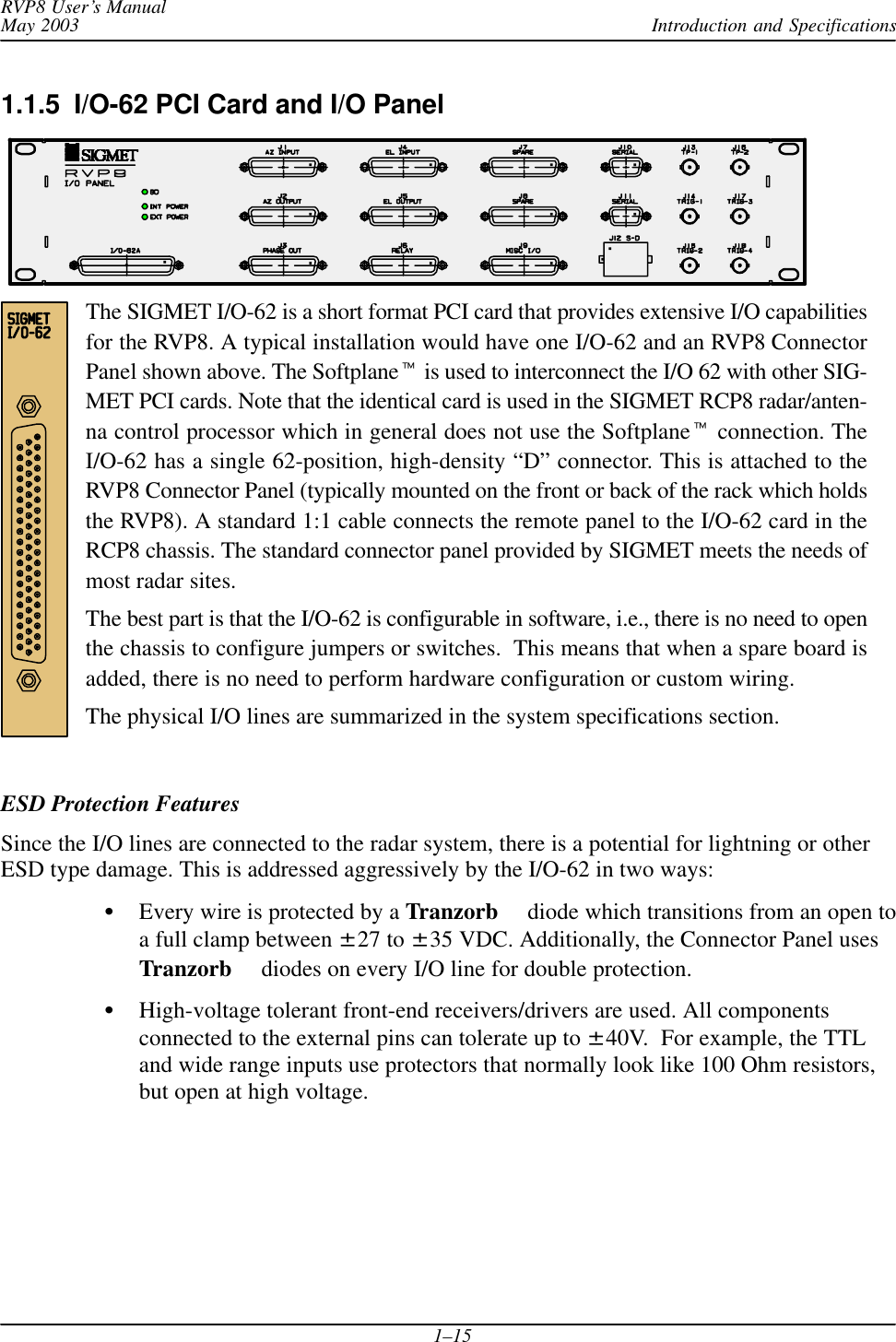
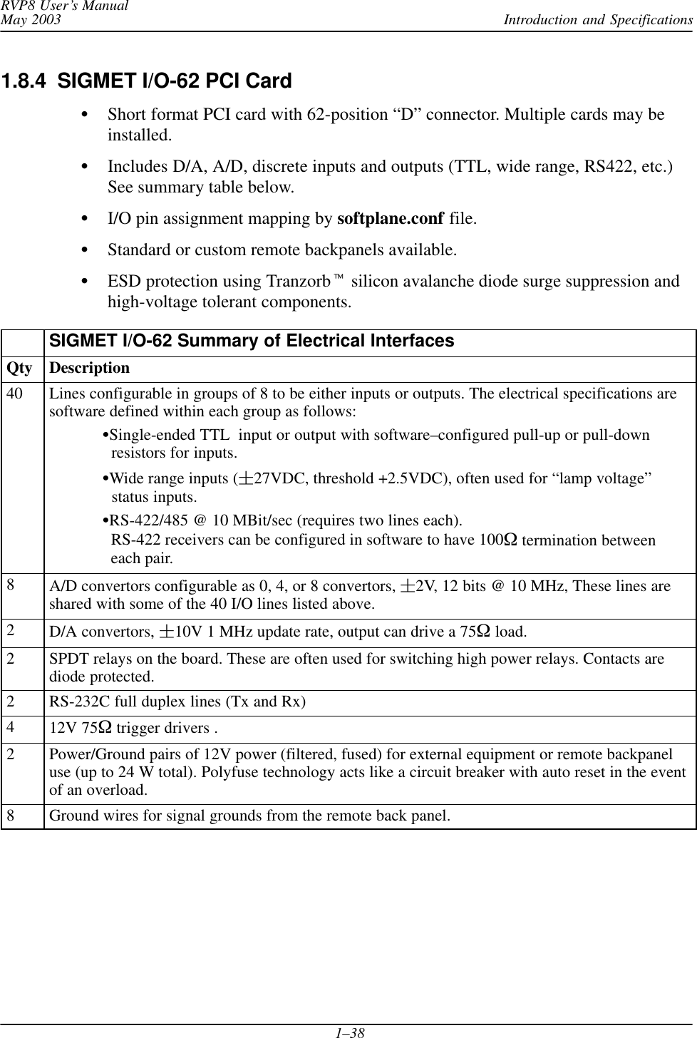
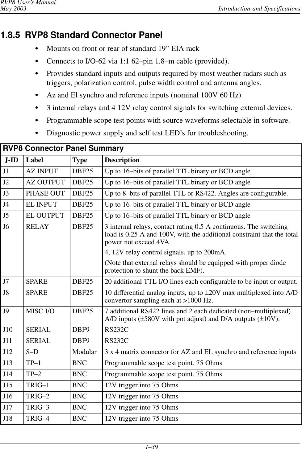
Introduction and SpecificationsRVP8 User’s ManualMay 20031–151.1.5  I/O-62 PCI Card and I/O PanelThe SIGMET I/O-62 is a short format PCI card that provides extensive I/O capabilitiesfor the RVP8. A typical installation would have one I/O-62 and an RVP8 ConnectorPanel shown above. The Softplane is used to interconnect the I/O 62 with other SIG-MET PCI cards. Note that the identical card is used in the SIGMET RCP8 radar/anten-na control processor which in general does not use the Softplane connection. TheI/O-62 has a single 62-position, high-density “D” connector. This is attached to theRVP8 Connector Panel (typically mounted on the front or back of the rack which holdsthe RVP8). A standard 1:1 cable connects the remote panel to the I/O-62 card in theRCP8 chassis. The standard connector panel provided by SIGMET meets the needs ofmost radar sites.The best part is that the I/O-62 is configurable in software, i.e., there is no need to openthe chassis to configure jumpers or switches.  This means that when a spare board isadded, there is no need to perform hardware configuration or custom wiring.The physical I/O lines are summarized in the system specifications section.ESD Protection FeaturesSince the I/O lines are connected to the radar system, there is a potential for lightning or otherESD type damage. This is addressed aggressively by the I/O-62 in two ways:Every wire is protected by a Tranzorb  diode which transitions from an open toa full clamp between ±27 to ±35 VDC. Additionally, the Connector Panel usesTranzorb  diodes on every I/O line for double protection.High-voltage tolerant front-end receivers/drivers are used. All componentsconnected to the external pins can tolerate up to ±40V.  For example, the TTLand wide range inputs use protectors that normally look like 100 Ohm resistors,but open at high voltage.
Introduction and SpecificationsRVP8 User’s ManualMay 20031–16Run Time FPGA ConfigurationThe SIGMET I/O-62 card is built around a 100K–Gate FPGA which, in addition to driving theI/O signals on the 62-position  connector, also coordinates the PCI and Softplane traffic. Thesechips are SRAM–based, meaning that they are configured at run time. This allows the FPGAcode to be automatically upgraded during each RVP8 code release without needing to physicallyreprogram any parts.The board’s basic I/O services use up only 40% of the complete FPGA. The leftover spacemakes it possible to add smart processing right on the I/O-62 board to handle custom needs. Forexample the 16–bit floating–point (I,Q) data in the previous example could be reformatted into a32–bit fixed–point stream. Other examples include generating custom serial formats, datadebouncing, and signal transition detection. In general, I/O functions that would either betedious or inappropriate for the host computer SBC  can likely be moved onto the I/O-62 carditself.
Introduction and SpecificationsRVP8 User’s ManualMay 20031–171.2  Comparison of Analog vs Digital Radar Receivers1.2.1  What is a Digital IF Receiver?A digital IF receiver accepts the analog IF signal (typically 30 MHz), processes it and outputs astream of wide dynamic range digital “I” and “Q” values. These quantities are then processed toobtain the moment data (e.g., Z, V, W or polarization variables). Additionally, the digitalreceiver can accept the transmit pulse “burst sample” for the purpose of measuring thefrequency, phase and power of the transmit pulse. The functions that can be performed by thedigital receiver are:IF band pass filtering“I” and “Q” calculation over wide dynamic rangePhase measurement and correction of transmitted pulse for magnetron systems –from burst sampleAmplitude measurement and correction of transmitted pulse – from burst sampleFrequency measurement for AFC output – from burst sampleThe digital approach replaces virtually all of the traditional IF receiver components with flexiblesoftware-controlled modules that can be easily adapted to function for a wide variety of radarsand operational requirements.The digital receiver approach made a very rapid entry into the weather radar market. Up untilthe about 1997 weather radars were not supplied with digital receivers. Today in 2003 nearly allnew weather radars and weather radar upgrades use the digital receiver approach. Much of thisrapid change is attributed to the previous generation RVP7 which is the most widely soldweather radar signal processor of all time.The number one advantage of a digital receiver is that it achieves a wide linear dynamic range(e.g., >95dB depending on pulse width) without having to use AGC circuits which are complexto build, calibrate and maintain. However, there are other advantages as well:Lower initial cost by eliminating virtually all IF receiver components.Lower life cycle cost do to reduced maintenance.Selectable IF frequency.Software controlled AFC with automatic alignment.Programmable band pass filterDual or multiple IF multiplexingImproved remote monitoring down to the IF level.The following sections compare the digital receiver approach to the analog receiver approach.This illustrates the advantages of the digital approach and what functions are performed by adigital receiver.
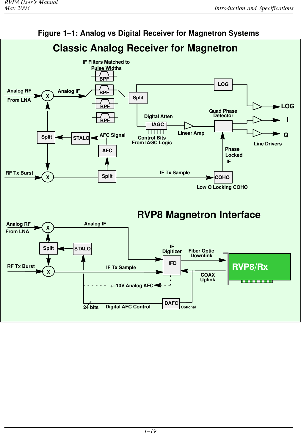
Introduction and SpecificationsRVP8 User’s ManualMay 20031–181.2.2  Magnetron Receiver ExampleA typical analog receiver for a magnetron system is shown in the top portion of Figure 1–1.  Thereceived RF signal from the LNA is first mixed with the STALO (RF–IF) and the resulting IFsignal is applied to one of several bandpass filters that match the width of the transmitted pulse.The filter selection is usually done with relays.  The narrow band waveform is then split.  Half isapplied to a LOG amplifier having a dynamic range of 80–100dB, from which a calibratedmeasurement of signal power can be obtained.  The LOG amplifier is required because it isalmost impossible to build a linear amplifier with the required dynamic range.  However, phasedistortion within the LOG amplifier renders it unsuitable for making Doppler measurements;hence, a separate linear channel is still required.The linear amplifier is fed from the other half of the bandpass filter split.  It may be preceded bya gain control circuit (IAGC) which adjusts the instantaneous signal strength to fall within thelimited dynamic range of the linear amplifier.  The amplitude and phase characteristics of theIAGC attenuator must be calibrated so that the “I” and “Q” samples may be corrected duringprocessing.The IF output from the linear amplifier is applied to a pair of mixers that produce “I” and “Q”.The mixer pair must have very symmetric phase and gain characteristics, and each must besupplied with an accurate 0-degree and 90-degree version of the Coherent Local Oscillator(COHO).  The later is usually obtained by sampling a portion of the transmitted pulse, and thenphase locking an oscillator (COHO) that continues to “ring” afterward.  Phase locked COHO’sof this sort can be very troublesome – they often fail to lock properly, drift with age, and fail tomaintain coherence over the full unambiguous range.The transmit burst that locks the COHO is also used by the Automatic Frequency Control (AFC)loop.  The AFC relies on an FM discriminator and low pass filter to produce a correction voltagethat maintains a constant difference between the magnetron frequency and the reference STALOfrequency.  The AFC circuit is often troublesome to set and maintain.  Also, since it operatescontinuously, small phase errors are continually being introduced within each coherentprocessing interval.In contrast, the RVP8 digital receiver is shown in to lower portion of  Figure 1–1.  The only oldparts that still remain are the microwave STALO oscillator, and the mixer that produces thetransmit burst. The burst pulse and the analog IF waveform are cabled directly into the IFD onSMA coax cables.  Likewise, the AFC control voltage is also a simple direct connection eitherwith analog tuning (+–10V from IFD) or digital control via the optional DAFC interface.  Thesecables constitute the complete interface to the radar’s internal signals; no other connections arerequired within the receiver cabinet.
Introduction and SpecificationsRVP8 User’s ManualMay 20031–19Figure 1–1: Analog vs Digital Receiver for Magnetron SystemsClassic Analog Receiver for MagnetronAnalog IF IFDigital AttenControl BitsIAGCSplitLOGLinear AmpQuad PhaseDetectorCOHORVP8 Magnetron InterfaceAnalog IFFrom IAGC LogicIFDigitizer Fiber OpticRF Tx BurstSplitXSplitAFCIF Tx SampleIF Tx SampleXDigital AFC ControlCOAXUplinkAFC SignalIQLOGLine DriversLow Q Locking COHOIF Filters Matched toPulse WidthsBPFBPFBPFIFDDownlinkDAFC+–10V Analog AFCXXAnalog RFFrom LNABPFAnalog RFFrom LNASplit24 bitsPhaseLockedRVP8/RxOptionalSTALORF Tx BurstSTALO
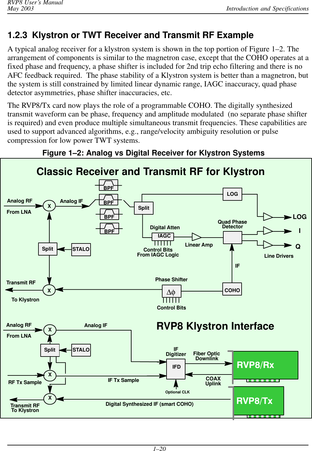
Introduction and SpecificationsRVP8 User’s ManualMay 20031–201.2.3  Klystron or TWT Receiver and Transmit RF ExampleA typical analog receiver for a klystron system is shown in the top portion of Figure 1–2. Thearrangement of components is similar to the magnetron case, except that the COHO operates at afixed phase and frequency, a phase shifter is included for 2nd trip echo filtering and there is noAFC feedback required.  The phase stability of a Klystron system is better than a magnetron, butthe system is still constrained by limited linear dynamic range, IAGC inaccuracy, quad phasedetector asymmetries, phase shifter inaccuracies, etc.The RVP8/Tx card now plays the role of a programmable COHO. The digitally synthesizedtransmit waveform can be phase, frequency and amplitude modulated  (no separate phase shifteris required) and even produce multiple simultaneous transmit frequencies. These capabilities areused to support advanced algorithms, e.g., range/velocity ambiguity resolution or pulsecompression for low power TWT systems.Figure 1–2: Analog vs Digital Receiver for Klystron SystemsClassic Receiver and Transmit RF for KlystronCOHORVP8 Klystron InterfaceTransmit RFXTo KlystronAnalog IF IFDigital AttenControl BitsIAGCSplitLOGLinear AmpQuad PhaseDetectorFrom IAGC LogicSplitIQLOGLine DriversBPFBPFBPFXAnalog RFFrom LNABPFAnalog IFIFDigitizer Fiber OpticIF Tx SampleRF Tx SampleXDigital Synthesized IF (smart COHO)COAXUplinkIFDDownlinkXAnalog RFFrom LNASplitXTransmit RFTo KlystronOptional CLKRVP8/TxRVP8/Rx∆φPhase ShifterControl BitsSTALOSTALO
Introduction and SpecificationsRVP8 User’s ManualMay 20031–211.3  RVP8 IF Signal Processing1.3.1  IFD Data Capture and TimingThe RVP8 design concept is to perform very little signal processing within the IFD digitizermodule itself.  This is to minimize the presence of digital components that might interfere withthe clean capture of the IF signals.The digitized IF and burst pulse samples are multiplexed onto the fiber channel link whichprovides the digital data to the RVP8/Main board at approximately 540-MBits/sec. The 14-bitsamples are encoded for transmission over a fiber channel link.  This optical link allows the IFDto be as far as 100 meters away from the RVP8/Main board and provides an added degree ofnoise immunity and isolation.The uplink input from the RVP8/Main board provides the timing for multiplexing the burst pulsesample with the IF signal. In addition, it is used to set the AFC DAC or digital output level, andto perform self tests.The sample clock oscillator in the IFD is selected to be very stable. The sample clock serves asimilar function to the COHO on a traditional Klystron system, i.e., it is the master time keeper.Because of this the IFD sample clock is used to phase lock the entire RVP8, i.e., the Rx, Tx,IO-62 boards and the SoftPlane are all phase locked to the IFD sample clock. Designers havetwo choices for factory configuration of the IFD sample clock:A fixed crystal frequency selected to achieve a desired range resolution. Thestandard range resolution corresponds to 25 m increments.A very narrow band VCXO (50 ppm) selected to lock to an input reference signalfrom the radar, and provide a desired range resolution.  SIGMET stocks VCXO’sfor 25 m range resolution increments for reference inputs of 10, 20, 30 and 60MHz. Custom frequency VCXO’s are available on request. Examples of externalreference signal sources are an external COHO, external STALO reference orperhaps even a GPS clock).
Introduction and SpecificationsRVP8 User’s ManualMay 20031–221.3.2  Burst Pulse Analysis for Amplitude/Frequency/PhaseThe burst pulse analysis provides the ampli-tude, frequency and phase of the transmittedpulse. The phase measurement is analogous tothe COHO locking that is performed by a tradi-tional magnetron radar. The difference is thatthe phase is known in the digital technique, sothat range dealiasing using the phase modula-tion techniques is possible. Amplitude mea-surement (not performed by traditional radars)can provide enhanced performance by allow-ing the “I” and “Q” values to be corrected forvariations in the both the average and the pulse-to-pulse transmitted power. In addition, awarning is issued if the burst pulse amplitudefalls below a threshold value.The burst pulse data stream is first analyzed by an adaptive algorithm to locate the burst pulsepower envelope (e.g. 0.8 sec). The algorithm first does a coarse search for the burst pulse in thetime/frequency domain (by scanning the AFC) and then does a fine search in both time andfrequency, to assure that the burst is centered at “range 0” and is at the required IF value. Thepower-weighted phase of the burst pulse and the total burst pulse power is then computed. Thepower weighted average phase is used to make the digital phase correction. Phase jitter formagnetron systems with good quality modulator and STALO is better than 0.5 degrees RMS, asmeasured on actual nearby clutter targets. For Klystron systems, the phase locking is better than0.1 degree RMS.The burst pulse frequency is also analyzed to calculate the frequency error from the nominal IFfrequency.  For magnetron systems, the error is filtered with a selectable time constant which istypically set to several minutes to compensate for slow drift of the magnetron. The digitalfrequency error is sent via the uplink to the IFD in the receiver cabinet where a DAC converts itinto an analog output to the magnetron STALO. Optionally, a DAFC unit can be Teed off theuplink cable to interface to Klystron systems do not require the AFC.
Introduction and SpecificationsRVP8 User’s ManualMay 20031–231.3.3  Rx Board and CPU IF to I/Q ProcessingFigure 1–3: IF to I/Q Processing Steps Fiber OpticReceiverDigital IFIF Tx SamplesBandpass FilterDigital Quad Phaseand DecompressionTx Burst PulseAnalysisFrequencyAmplitude/Phase CorrectionInterferenceFilterAFCServoI/QSignal I/Q TxBurstIFD Fiber OpticDownlinkIFD COAXUplinkDigitized IF Signaland Tx Burst SampleTiming and digital AFCIF to I/Q Processing Steps1000 BaseTEthernetUDP Broadcast I/QSamples to recordingsystem or separateprocessing systemDigital FIRRVP8/RxCPUPCII/QDigital AFCI/Q MomentProcessingIF TxSamplesI/QTx BurstI/QSignalI/Q TimeSeriesAPIThe RVP8/Rx board performs the initial processing of the IF digital data stream and outputs “I”and “Q” data values to the host computer via the PCI bus. In addition, the frequency, phase andamplitude of the burst pulse are measured. The functions performed by the processor are:Reception of the digital serial fiber optic data stream.Band pass filtering  of the IF signal using configurable digital FIR filter matchedto the pulsewidth.Range gating and optional coherent averaging (essentially performed during theband pass filtering step).
Introduction and SpecificationsRVP8 User’s ManualMay 20031–24Computation of “I” and “Q” quadrature values (also performed during the bandpass filtering step).Transmit burst sample frequency, phase and amplitude calculationI and Q phase and amplitude correction based on transmit burst sample.Interference rejection algorithm.AFC frequency error calculation with output to IFD for digital or analog controlof STALO (for magnetron systems).The advantage of the digital approach is that the software algorithms for these functions can beeasily changed. Configuration information (e.g., processor major mode, PRF, pulsewidth, gatespacing, etc.) is supplied from the host computer.The digital matched filter that computes “I”and “Q” is designed in an interactive man-ner using a TTY and oscilloscope for graph-ical display.  The filter’s passband widthand impulse response length are chosen bythe user, and the RVP8 constructs the filtercoefficients using built-in design software.The frequency response of the filter can bedisplayed and compared to the frequencycontent of the actual transmitted pulse.Microwave energy can come from a variety of transmitters such as ground-based, ship-based orairborne radars as well as communications links. These can cause substantial interference to aweather radar system. Interference rejection is provided as standard in the RVP8. Three differentinterference rejection algorithms are supported.The RVP8/Rx board places the wide dynamic range “I” and “Q” samples directly on the PCIbus where they are sent to the processor section of the PC (e.g., dual Pentium processors on asingle-board computer or motherboard).  The I/Q values are then processed on the Pentiumprocessors to extract the moment information (Z, V, W and optional polarization parameters).The I and Q values can also be placed on a gigabit Ethernet line (1000 BaseT) which is provideddirectly on the processor board. This means that there is no second PCI bus “hit” required tosend the data to a recording system or a completely separate processing system.
Introduction and SpecificationsRVP8 User’s ManualMay 20031–251.4  RVP8 Weather Signal ProcessingThe processing of weather signals by the RVP8 is based on the algorithms used in the previousgeneration RVP7 and RVP6. However, the performance of the RVP8 allows a different approachto some of the processing algorithms, especially the frequency domain spectrum processing. Allof the algorithms start with the wide dynamic range I and Q samples that are obtained from theRx card over the PCI bus.The resulting intensity, radial velocity, spectrum width and polarization measurements are thensent to a separate host computer to serve as input for applications such as:Quantitative Rainfall MeasurementVertical Wind ProfilingZDR Hail DetectionTornado Detection and Microburst DetectionGust Front DetectionParticle IdentificationTarget Detection and TrackingGeneral Weather MonitoringTo obtain the basic moments, the RVP8 offers the option of several major processing modes:Pulse Pair Mode Time Domain ProcessingDFT/FFT Mode Frequency Domain ProcessingRandom Phase Mode for 2nd trip echo filteringPolarization Mode ProcessingNote that the RVP8 is the first commercial processor to perform discrete Fourier transforms(DFT) as well as fast Fourier transforms (FFT). FFT is more computationally efficient thanDFT, but the sample size is limited to be a power of two (16, 32, 64, ...) This is too restrictive onthe scan strategy for a modern Doppler radar since this means, for example, that a one degreeazimuth radial must be constructed from say exactly 64 input I/Q values. The RVP8 has theprocessing power such that when the sample size is not a power of 2, a DFT is performed insteadof an FFTThese modes share some common features that are described first, followed by descriptions ofthe unique features of each mode.
Introduction and SpecificationsRVP8 User’s ManualMay 20031–261.4.1  General Processing featuresFigure 1–4 shows a block diagram of the processing steps. These are discussed below.AutocorrelationsThe autocorrelations R0, R1 and R2 are produced by all three processing modes. However, theway that they are produced is different for the three modes, particularly with regard to thefiltering that is performed.Pulse Pair Mode– Filtering for clutter is performed in the time domain.Autocorrelations are computed in the time domain.DFT/FFT Mode– Filtering for clutter is performed in the frequency domain by anadaptive algorithm. Autocorrelations are computed from the inverse transform.Random Phase– Filtering for clutter and second trip echo is performed in thefrequency domain by adaptive algorithms. Autocorrelations are computed fromthe inverse transform.Figure 1–4: I/Q Processing for Weather Moment Extraction Moment  andThresholdCalculationsClutter FilterIQAutocorrelationsRVP8 Standard Moment Processing StepsClutter MicroSuppression andRange AveragingThresholdingSpeckle FilterTZVWSQILOGSIGCCORT0R0R1R2T0R0R1R2TZVWPulse Pair, FFT/DFT, Random Phase Modes10/100/1000 BaseT EthernetTo Applications Host ComputerTime SeriesAPIThe use of the R2 lag provides improved estimation of signal-to-noise ratio and spectrum width.Processors that do not use R2 cannot effectively measure the SNR and spectrum width.
Introduction and SpecificationsRVP8 User’s ManualMay 20031–27Time (azimuth) AveragingThe autocorrelations are based on input “I” and “Q” values over a selectable number of pulsesbetween 8, 9, 10, ...,256. Any integer number of pulses in this interval may be used includingDFT/FFT and random phase modes.Selectable angle synchronization using the input AZ and EL tag lines assures that all possiblepulses are used during averaging for each, say, 1 degree interval. This minimizes the number of“wasted” pulses for maximum sensitivity. Azimuth angle synchronization also assures theaccurate vertical alignment of radial data from different elevation angles in a volume scan (seebelow).TAG Angle Samples of Azimuth and Elevation During data acquisition and processing it is usually necessary to associate each output ray withan antenna position.  To make this task simpler the RVP8 samples 32 digital input “TAG” lines,once at the beginning and once at the end of each data acquisition period.  These samples areoutput in a four-word header of each processed ray.  When connected to antenna azimuth andelevation, the TAG samples provide starting and ending angles for the ray, from which themidpoint could easily be deduced.  Since the bits are merely passed on to the user, any anglecoding scheme may be used.  The processor also supports an angle synchronization mode, inwhich data rays are automatically aligned with a user-defined table of positions.  For thatapplication, angles may be input either in binary or BCD.Range Averaging and Clutter Microsuppression To improve the accuracy of the reflectivity measurements, the RVP8 can perform rangeaveraging.  When this is done, autocorrelations from consecutive range bins are averaged, andthe result is treated as if it were a single bin.  This type of averaging is useful to lower thenumber of range bins that the host computer must process.Range averaging of the autocorrelations may be performed over 2, 3, 4, ..., 16 bins. Prior torange averaging, any bins that exceed the selectable clutter-to-signal threshold are discarded.This prevents isolated strong clutter targets from corrupting the range average, which improvesthe sub-clutter visibility.Moment ExtractionThe autocorrelations serve as the basis for the Doppler moment calculations,Mean velocity – from Arg [ R1 ]Spectrum width – from |R1| and |R2| assuming Gaussian spectrumdBZ – from R0 with correction for ground clutter, system noise and gaseousattenuation. Uses calibration information supplied by host computer.dBT – identical to dBZ except without ground clutter.These are the standard parameters that are output to the host computer on the high-speedEthernet interface.
Introduction and SpecificationsRVP8 User’s ManualMay 20031–28ThresholdingThe RVP8 calculates several parameters that are used to threshold (discard) bins with weak orcorrupted signals. The thresholding parameters are:Signal quality index (SQI=|R1|/R0)LOG (or incoherent) signal-to-noise ratio (LOG)SIG (coherent) signal-to-noise ratioCCOR clutter correctionThese parameters are computed for each range bin and can be applied in AND/OR logicalexpressions independently for dBZ, V and W.Speckle FilterThe speckle filter can be selected to remove isolated single bins of either velocity/width orintensity. This feature eliminates single pixel speckles which allows the thresholds to be reducedfor greater sensitivity with fewer false alarms (speckles). Both a 1D (single azimuth ray) and 2D(3 azimuth rays by 3 range bins) are supported.Velocity UnfoldingA special feature of the RVP8 processor is its ability to “unfold” mean velocity measurementsbased on a dual PRF algorithm.  In this technique two different radar PRF’s are used foralternate N-pulse processing intervals.  The internal trigger generator automatically produces thecorrect dual-PRF trigger, but an external trigger can also be applied.  In the later case, theENDRAY_ output line provides the indication of when to switch rates.  The RVP8 measures thePRF to determine which rate (high or low) was present on a given processing interval, and thenunfolds based on either a 2:3, 3:4 or 4:5 frequency ratio.  Table 1–1 gives typical unambiguousvelocity intervals for a variety of radar wavelengths and PRF’s.Table 1–1: Examples of Dual PRF Velocity UnfoldingUnambiguous Velocity (m/s) forVarious Radar WavelengthsPRF1 PRF2 UnambiguousRange (km) 3 cm 5 cm 10 cm500 * 300 3.75 6.25 12.50 NoU f ldi1000 * 150 7.50 12.50 25.00 Unfolding2000 * 75 15.00 25.00 50.00500 333 300 7.50 12.50 25.00 TwoTi1000 667 150 15.00 25.00 50.00 TimesUnfolding2000 1333 75 30.00 50.00 100.00Unfolding
Introduction and SpecificationsRVP8 User’s ManualMay 20031–29PRF1 10 cm5 cm3 cmUnambiguousRange (km)PRF2500 375 300 11.25 18.75 37.50 Three TimesU f ldi1000 750 150 22.50 37.50 75.00 Unfolding2000 1500 75 45.00 75.00 150.00500 400 300 15.00 25.00 50.00 FourTi1000 800 150 30.00 15.00 100.00 TimesUnfolding2000 1600 75 60.00 100.00 200.00Unfolding1.4.2  RVP8 Pulse Pair Time Domain ProcessingPulse pair processing is done by direct calculation of the autocorrelation.  Prior to pulse pairprocessing, the input “I” and “Q” values are filtered for clutter using a a time domain notchfilter. Filters of various selectable widths are available for either 40 or 50 dB stop bandattenuation. The filtered I/Q values are processed to obtain the autocorrelation lags R0, R1 andR2. The unfiltered power is also calculated (T0). The autocorrelations  are then sent to the rangeaveraging and moment extraction steps.1.4.3  RVP8 DFT/FFT Processing The DFT/FFT mode allows clutter cancelation to be performed in the frequency domain. DFT isused in general, with FFT’s used if the requested sample size is a power of 2.Three standard windows are supported to provide the best match of window width to thespectrum dynamic range:RectangularHammingBlackmanAfter the FFT step, clutter cancelation is done using a selectable fixed width filter thatinterpolates across the noise or any overlapped weather or an adaptive filter which automaticallydetermines the optimal width. This technique preserves overlapped weather as compared to timedomain notch filters which will always attenuate overlapped weather to some extent, dependingon the spectrum width. After clutter cancelation, R0, R1 and R2 are computed by inversetransform and these are used for moment estimation.
Introduction and SpecificationsRVP8 User’s ManualMay 20031–301.4.4  Random Phase Processing for 2nd Trip EchoSecond trip echoes can be a serious problem for applications that require operation at a highPRF. Second trip echoes can appear separately or can be overlaid on first trip echoes (second tripobscuration). The random phase technique separates the first and second trip echoes so that:In nearly all cases, the 2nd trip echo can be removed from the first trip even in thecase of overlapped 1st and 2nd trip echoes. The benefit is a clean first trip display.The 2nd trip echoes can be recovered and placed at their proper range at 1sttrip/2nd trip signal ratios of up to 40 dB difference for overlapped echoes.Because of the wide dynamic range of weather echoes, this power limit willsometimes be exceeded.The technique requires that the phase of each pulse be random. Digital phase correction is thenapplied in the processor for the first and second trips. The critical step is the adaptive filterwhich removes the echo of the other trip to increase the SNR. Magnetrons have a naturallyrandom phase. For Klystron radars, a digitally controlled precision IF phase shifter is required.The RVP8 provides an 8-bit RS422 output for the phase shifter.For more information on the technique refer to Joe, et. al., 1995.1.4.5  Polarization Mode ProcessingPolarization processing uses a time domain autocorrelation approach to calculate the variousparameters of the polarization co-variance matrix, i.e., ZDR, LDR, PHIDP, RHOHV, PHIDP(KDP), etc. In addition, the standard moments T, V, Z, W are also calculated. Which parametersare available and which algorithms are used to calculate them depends on the type ofpolarization radar, e.g., single channel switching, simultaneous transmit and receive (STAR),dual channel switching. SIGMET, Inc. is licensed by US National Severe Storms Laboratory(NSSL) to use the STAR hardware and processing techniques and algorithms.Polarization measurements require special calibration of the ZDR and LDR offsets. The use of aclutter filter for the polarization variables can sometimes bias the derived parameters. Because ofthis, the user decides whether or not to use filtered or unfiltered time series.1.4.6  Output DataThe RVP8 output data for standard moment calculations consist of mean radial velocity (V),Spectrum Width (W), Corrected Reflectivity(Z or dBZ) and Uncorrected Reflectivity (T ordBT). Other data outputs include I/Q time series, DFT/FFT power spectrum points andpolarization parameters. The output can be made in either 8 or 16-bit format. 8-bit format ispreferred over 16-bit format for most applications since the accuracy is more than adequate foran operational radar system, and the data communications are reduced by 50%. 16-bit formatsare sometimes used by research customers for data archive purposes. Note that time series andFFT are always 16-bit formats. All data formats are documented in Chapter 6 of this manual.A standard output is the I/Q time series on gigabit network (1000 BaseT). These are sent viaUDP broadcast to an I/Q archiving system or even a completely independent parallel processingsystem.
Introduction and SpecificationsRVP8 User’s ManualMay 20031–311.5  RVP8 Control and Maintenance Features1.5.1  Radar Control FunctionsThe RVP8 also performs several important radar control functions:Trigger generation- up to 6 programmable triggers.Pulsewidth control (four states controlled by four bits).Angle/data synchronization- to collect data at precise azimuth intervals (e.g.,every 0.5, 1, 1.5 degrees) based on the AZ/EL angle inputs.Phase shifter- to control the phase on legacy Klystron systems. New or upgradeKlystron or TWT systems can use the RVP8/Tx card to provide very accuratephase shifting.ZDR switch control- for horizontal/vertical or other polarization switchingscheme.AFC output (digital or analog) based on the burst pulse analysis for magnetronsystems.Pulsewidth and trigger control are both built into the RVP8.  Four TTL output lines can beprogrammed to drive external relays that control the transmitter pulsewidth.  The internal triggergenerator drives six separate lines, each of which can be programmed to produce a desiredwaveform.  The trigger generator is unique in that the waveforms are stored in RAM and can bemodified interactively by user software.  Thus, precisely delayed and jitter-free strobes and gatescan easily be produced.  For each pulsewidth there is a corresponding maximum trigger rate thatcan be generated.  Note, however, that the RVP8 can also operate from an external user-suppliedtrigger.  In either case, the processor measures the trigger period between pulses so that usersoftware can monitor it as needed.The RVP8 also supports trigger blanking during which one or more (selectable) of the transmittriggers can be inhibited. Trigger blanking is used to avoid interference with other electronicequipment and to protect nearby personnel from radiation hazard. There are two techniques forthis:2D AZ/EL sector blanking areas can be defined in the RVP8 itself.An external trigger blanking signal (switch closure to ground, TTL or RS422) canbe supplied, for example from a proximity switch that triggers when the antennagoes below a safe elevation angle or connected to the radome access hatch.
Introduction and SpecificationsRVP8 User’s ManualMay 20031–321.5.2  Power-Up Setup ConfigurationThe RVP8 stores on disk an extensive set of configuration information.  The purpose of thesedata is to define the exact configuration of the RVP8 upon startup.  The setup information can beaccessed and modified using either a local keyboard and monitor, or over the network. Formultiple radar networks, the configuration management can be centrally administered bycopying tested “master” configuration files to the various network radars. It is not necessary togo to the radar to change ROM’s as was the case for previous generation processors.1.5.3  Built-In DiagnosticsOn power-up, the RVP8 performs a sequence of internal self-tests.  The test sequence requiresabout four seconds to perform, and tests approximately 95% of the internal digital circuitry.Errors are isolated to specific sections of the board as much as possible.  If any check fails, theuser can be certain that some component is not functioning correctly.  However, there is a verysmall chance that even a defective board may pass all the tests; the failure may be in one of thefew areas that can not be checked.The RVP8 displays the test results on the LED front panel (for a standard SIGMET chassis).  Inthis way, there is immediate visual confirmation of the diagnostic tests, even if the host computerhas not yet been connected.  The local keyboard and monitor or a networked workstation can beused to see the test results in the TTY menus or even invoke a power–up reset and test.
Introduction and SpecificationsRVP8 User’s ManualMay 20031–331.6  Support Utilities and Available Application SoftwareThe RVP8 system includes a complete set of tools for the calibration, alignment andconfiguration of the RVP8. These includes the following utilities:ascope- a comprehensive utility for manual signal processor control and datadisplay of moments, times series and Doppler spectra. ascope includes a realisticsignal simulator capable of producing both first and second trip targets.Recording/playback of time series and moments is included as well.dspx- an ASCII text-based program to access and control the signal processor,including providing access to the local setup menus. speed- a performance measuring utility.DspExport- exports the RVP8 to another workstation over the network. Thisallows utilities on a remote network to run locally, as opposed to exporting theutility display window over the network.setup- interactive GUI for creating/editing the RVP8 configuration files.zauto- calibration utility for use with a test signal generator.These tools can be run locally on the RVP8 itself or over the network from a central maintenancefacility. The DspExport utility improves the performance of the utilities for network applicationsby letting them be run on the workstation that is remote from the RVP8. Note that standardX–Window export is of course supported but requires more bandwidth.In addition, complete radar application software can be purchased from SIGMET:IRIS/Radar on a separate PC, interfaces to the RVP8 by 100 BaseT Ethernet.IRIS/Radar controls both the RVP8 and the SIGMET RCP8 radar/antenna controlprocessor.  The package provides complete local and remote control/monitoring,data processing and communication for a radar system.IRIS/Analysis (and options) runs on a separate PC, often at a central site. OneIRIS/Analysis can support up to 20 radar systems. This functions as a radarproduct generator (RPG) to provide outputs such as CAPPI, rain accumulations,echo tops, automatic warning and tracking, etc. Optional software packages areprovided for special applications: wind shear and microburst detection,hydrometeorology with raingage calibration and subcatchments, composite, dualDoppler and 3D Display.IRIS/Web provides IRIS displays to network users on standard PC’s (Windowsor Linux) running Netscape or Internet Explorer.IRIS/Display can display products sent to it and, with password authorization,can serve as a remote control and monitoring site for networked radar systems.Features such as looping, cross–section, track, local warning, annotation, etc. areall provided by IRIS/Display. Note that both IRIS/Analysis and IRIS/Radar haveall of the capabilities of IRIS/Display in addition to their own functions. Thismeans that any IRIS system can display products.
Introduction and SpecificationsRVP8 User’s ManualMay 20031–341.7  Open Architecture and Published APIThe RVP8 is largely software compatible with the RVP7, and uses the same published APIopcode interface that has evolved over the years from the RVP5, RVP6, and RVP7 products.Driver code that has been written for the RVP7 can be easily adapted to the RVP8. The 16–bitI/O command protocols are identical, and the data formats are unchanged. What is different isthat the RVP8 supports an Ethernet interface rather than only a SCSI interface. SIGMETprovides a free source code example for the driver in C.In addition to assuring backward compatibility, SIGMET also recognizes that certain users mayrequire the ability to write their own signal processing algorithms which will run on the RVP8.To accommodate this, the RVP8 software is organized to allow separately compiled plug-inmodules to be statically linked into the running code. The application program interface (API)allows user code to be inserted at the following stages of processing:Tx/Rx waveform synthesis and matched filter generation— The API allows thetransmit waveforms to be defined from pulse to pulse, along with thecorresponding FIR coefficients that will extract (I,Q) from that Tx waveform.This allows users to experiment with arbitrary waveforms for pulse compressionand frequency agility.Time series and spectra processing from (I,Q)- The API allows you to modify thedefault time series and spectra data, e.g., to perform averaging or windowing in adifferent way.Parameter generation from (I,Q)- This is probably where the greatest activity willoccur for user–supplied code. The API allows you to redefine how the standardparameters (dBZ, Velocity, Width, PHIDP, etc.) are computed from the incoming(I,Q) time series. You may also create brand new parameter types that are notincluded in the basic RVP8 data set.Note that the standard SIGMET algorithms are not made public in this model. Rather, theinterface hooks and development tools are provided so that users can add their own softwareextensions to the RVP8 framework. Many of the library routines that are fundamental to theRVP8 are also documented and can be called by user code; but the source to these routines is notgenerally released. Development tools which are not under public license must be purchasedseparately by the customer.While most customers will use the signal processing software supplied by SIGMET, the newopen software architecture approach employed by the RVP8 will be very useful to those researchcustomers who want to try innovative new approaches to signal processing, or to those OEMmanufacturers who are interested in having their own “custom” stamp on the product.
Introduction and SpecificationsRVP8 User’s ManualMay 20031–351.8  RVP8 Technical Specifications1.8.1  IFD Digitizer ModuleInput SignalsIF Received Signal: 50, + 6.5 dBm maxIF Magnetron Burst or COHO: 50, +6.5 dBm maxOptional Reference Clock: 2–60 MHz –10 to 0 dBmIF Ranges6 to 16MHz, 20-34 MHz, 38-52 MHz, 56-70 MHzLinear Dynamic Range90 to >100dB depending on pulsewidth/bandwidth filterA/D ConversionResolution 14 bit  with jitter  <2.5 picosecSampling rate 33.5 to 39.5 MHz (selectable, standard is 35.975 MHz)AFC OutputAnalog –10 to +10VOptional Digital AFC (DAFC) with up to 24 programmable output bits.Automatic 2-D (time/frequency) burst pulse search and fine tracking algorithms.Fiber Optic Down Link540 MHz optical link, 62.5/125-micron multimode ST cable.Coax Uplink75 electrically isolated (16K) from receiver’s ground.Maximum Separation from RVP8/Rx100 meters, with automatic calibration of round trip time and range correction.
Introduction and SpecificationsRVP8 User’s ManualMay 20031–361.8.2  RVP8/Rx PCI CardPulse Repetition Frequency50 Hz to 20 KHz  +0.1%, continuously selectable.IF Band Pass FilterProgrammable Digital FIR with software selectable bandwidth. Built-in filterdesign software with graphical user interface.Impulse ResponseUp to 3024 FIR filter taps, corresponding to approximately 84 sec impulseresponse length for 36 MHz IF samples.  These very long filters are intended foruse with pulse compression.Range ResolutionMinimum bin spacing of 25 meters  selectable in N*8.33 meter steps. Bins can bepositioned in a configurable range mask with resolution of N* the fundamentalbin spacing, or arbitrarily to an accuracy of  ±2.2 meters.Maximum RangeUp to 1024 kmNumber of Range BinsFull unambiguous range at minimum resolution or 2048 range bins (whichever isless).Electrical and Optical InterfacesReceives fiber-optic downlink from the RVP8/IFD, and generates the 75  coaxuplink to the RVP8/IFD.BNC #1 for trigger output (12V, 75), or pretrigger input.BNC #2 for trigger output (12V, 75).Data Output via PCI Bus16–bit I and Q values14-bit raw IF samples
Introduction and SpecificationsRVP8 User’s ManualMay 20031–371.8.3  RVP8/Tx PCI CardAnalog Waveform ApplicationsDigitally synthesized IF transmit waveform for pulse compression, frequencyagility, and phase modulation applications.Master clock or COHO signal to the radar; can be phase locked or free running,arbitrary frequency.Analog Output Waveform CharacteristicsTwo independent, digitally synthesized, analog output waveforms (BNC).  Thesetwo outputs are electrically identical and logically independent IF waveformsynthesizers that can produce phase modulated CW signals, finite duration pulses,compressed pulses, etc.Can drive up to +12dBm into 50.14-bit interpolating TxDAC provides 71dB Signal-to-Noise Ratio.IF center frequency selectable from 8 to 32.4 MHz, and from 48.6 to 75MHz.Signal bandwidth as large as 15MHz for wideband/multiband Tx applications.Total harmonic distortion less than –74dB.Waveform pre-emphasis compensates for both static and dynamic Txnonlinearities.Other I/O signalsClock In/Out 50 SMA connector.  This can receive a CW reference frequencyto which the RVP8/Tx can lock to a P/Q frequency multiple (much like theRVP8/IFD can lock to an external reference).  This connector can also supply theTxData Clock, optionally divided by some N between 1 and 16, in order tosupply external circuitry with +10dBm clock reference at 50.9-pin “D” connector supporting four RS-422 differential signals formiscellaneous input and output with SoftPlane support..  Each line pair canoperate as a transmitter or as a receiver depending on what’s needed.  Possibleuses are: alternate reference clock input, gating input for CW modes, additionaltrigger outputs, external phase shift requests, etc.
Introduction and SpecificationsRVP8 User’s ManualMay 20031–381.8.4  SIGMET I/O-62 PCI CardShort format PCI card with 62-position “D” connector. Multiple cards may beinstalled.Includes D/A, A/D, discrete inputs and outputs (TTL, wide range, RS422, etc.)See summary table below.I/O pin assignment mapping by softplane.conf file.Standard or custom remote backpanels available.ESD protection using Tranzorb silicon avalanche diode surge suppression andhigh-voltage tolerant components.SIGMET I/O-62 Summary of Electrical InterfacesQty Description40 Lines configurable in groups of 8 to be either inputs or outputs. The electrical specifications aresoftware defined within each group as follows:Single-ended TTL  input or output with software–configured pull-up or pull-down  resistors for inputs.Wide range inputs (27VDC, threshold +2.5VDC), often used for “lamp voltage”   status inputs.RS-422/485 @ 10 MBit/sec (requires two lines each).   RS-422 receivers can be configured in software to have 100 termination between  each pair.8A/D convertors configurable as 0, 4, or 8 convertors, 2V, 12 bits @ 10 MHz, These lines areshared with some of the 40 I/O lines listed above.2D/A convertors, 10V 1 MHz update rate, output can drive a 75 load.2SPDT relays on the board. These are often used for switching high power relays. Contacts arediode protected.2RS-232C full duplex lines (Tx and Rx)412V 75 trigger drivers .2Power/Ground pairs of 12V power (filtered, fused) for external equipment or remote backpaneluse (up to 24 W total). Polyfuse technology acts like a circuit breaker with auto reset in the eventof an overload.8Ground wires for signal grounds from the remote back panel.
Introduction and SpecificationsRVP8 User’s ManualMay 20031–391.8.5  RVP8 Standard Connector PanelMounts on front or rear of standard 19” EIA rackConnects to I/O-62 via 1:1 62–pin 1.8–m cable (provided).Provides standard inputs and outputs required by most weather radars such astriggers, polarization control, pulse width control and antenna angles.Az and El synchro and reference inputs (nominal 100V 60 Hz)3 internal relays and 4 12V relay control signals for switching external devices.Programmable scope test points with source waveforms selectable in software.Diagnostic power supply and self test LED’s for troubleshooting.RVP8 Connector Panel Summary J-ID Label Type DescriptionJ1 AZ INPUT DBF25 Up to 16–bits of parallel TTL binary or BCD angleJ2 AZ OUTPUT DBF25 Up to 16–bits of parallel TTL binary or BCD angleJ3 PHASE OUT DBF25 Up to 8–bits of parallel TTL or RS422. Angles are configurable.J4 EL INPUT DBF25 Up to 16–bits of parallel TTL binary or BCD angleJ5 EL OUTPUT DBF25 Up to 16–bits of parallel TTL binary or BCD angleJ6 RELAY DBF25 3 internal relays, contact rating 0.5 A continuous. The switchingload is 0.25 A and 100V, with the additional constraint that the totalpower not exceed 4VA.4, 12V relay control signals, up to 200mA.(Note that external relays should be equipped with proper diodeprotection to shunt the back EMF).J7 SPARE DBF25 20 additional TTL I/O lines each configurable to be input or output.J8 SPARE DBF25 10 differential analog inputs, up to ±20V max multiplexed into A/Dconvertor sampling each at >1000 Hz.J9 MISC I/O DBF25 7 additional RS422 lines and 2 each dedicated (non–multiplexed)A/D inputs (±580V with pot adjust) and D/A outputs (±10V).J10 SERIAL DBF9 RS232CJ11 SERIAL DBF9 RS232CJ12 S–D Modular 3 x 4 matrix connector for AZ and EL synchro and reference inputsJ13 TP–1 BNC Programmable scope test point. 75 OhmsJ14 TP–2 BNC Programmable scope test point. 75 OhmsJ15 TRIG–1 BNC 12V trigger into 75 OhmsJ16 TRIG–2 BNC 12V trigger into 75 OhmsJ17 TRIG–3 BNC 12V trigger into 75 OhmsJ18 TRIG–4 BNC 12V trigger into 75 Ohms
Introduction and SpecificationsRVP8 User’s ManualMay 20031–401.8.6  RVP8 Processing AlgorithmsInput from Rx Board16–bit I/Q samplesOptional dual-channel I/Q samples (e.g., for polarization systems or dualfrequency systems)IQ Signal Correction OptionsAmplitude jitter correction based on running average of transmit power fromburst pulse.Interference correction for single pulse interferenceSaturation correction (3 to 5 dB)Primary Processing ModesPoly-Pulse Pair (PPP)FFTRandom or Phase Coded 2nd trip echo filtering/recoveryOptional Polarization with full co-variance matrix (ZDR, PHIDP, LDR, RHOHV,etc.)Optional Pulse CompressionProcessing OptionsFIR Clutter filters (40 and 50 dB) in pulse pair mode.Adaptive width clutter filters in FFT and phase coded 2nd trip mode.Velocity De-Aliasing: Dual PRF Velocity unfolding  at 3:2, 4:3 and 5:4 PRFratios or Dual PRT Velocity processing for selectable inter-pulse intervals.Range De-aliasing: Phase coding method (random phase formagnetron) Frequency coding method (not available for magnetron)Scan angle synchronization for data acquisition.Pulse integration up to 1024Corrections for gaseous attenuation and 1/R2.Up to 4 pulse widthsData OutputsdBZ Calibrated equivalent radar reflectivity 8 or 16 bits
Introduction and SpecificationsRVP8 User’s ManualMay 20031–41V Mean radial velocity8 or 16 bitsW Spectrum width8 or 16 bitsI/Q Time series16 bits each per sampleFFT Doppler Spectrum output option in FFT mode16 bits per componentOptional: ZDR, PHIDP, RHOHV, LDR, RHO8 or 16 bitsData Quality ThresholdsSignal–to–noise  ratio (SNR) Used to reject bins having weaksignals.  Typically applied to  dBZ.Signal quality index (SQI) Used to reject bins having incoherent(non–Doppler) signals.  Typically applied to mean velocity and width.Clutter–to–signal  ratio (CSR) Used to reject range bins having verystrong clutter.   Typically applied to mean velocity, width and dBZ.Speckle  Filter 2D filter removes single–bin targets such as aircraftor noise Fills isolated missing pixels as well.
Introduction and SpecificationsRVP8 User’s ManualMay 20031–421.8.7  RVP8 Input/Output SummaryDigital IF Serial Stream InputOn fiber optic cable from IFD for signal and burst sample. 16–bits @ 36 MHz(nominal).Ethernet or SCSI-2 Input/Output from Host ComputerData output of calibrated dBZ, V and W during normal operation. Diagnosticoutput of I and Q or FFT Doppler spectrum. Signal processor configuration andverification read–back is performed via the SCSI or Ethernet interface.RS-232C Serial Data I/OFor real time display/monitoring or data remoting.Serial AZ/EL angle tag input using standard SIGMET RCP format.AZ/EL Parallel Tag Line InputsUp to 16–bit each parallel TTL binary or BCD angles.Trigger Output6 TTL triggers on 75 BNC or 10V on 75 BNC (selectable for each trigger).Triggers are programmable with respect to trigger start, trigger width and sense(normal or inverted).Optional ZDR ControlRS-422 differential control for polarization switch.
Introduction and SpecificationsRVP8 User’s ManualMay 20031–431.8.8  Physical and Environmental CharacteristicsPackagingMotherboard Configuration 4U rackmount with 6 PCI slotsSingle Board Computer Configuration 4u rackmount with 14 PCI slotsCustom PC configurations available or packaged by customer.Dimensions of standard 4U chassis43.2 wide x 43.2  long x 17.8 cm high17   wide x 17 long x 7.00 inch  highDimensions IF Digitizer2.5 wide  x  10.9 long  x  23.6 cm high  1  wide  x  4.3   long x  9.3 inch    highRedundant Power Supplies. Three hot–swap modules with audio failure alarm.Input PowerIFD  100–240 VAC 47–63 Hz auto–rangingMain Chassis 60/50 Hz 115/230 VAC Manual SwitchesPower ConsumptionRVP8/Main Processor 180 Watts with Rx and SBCRVP8/IFD IF Digitizer 12 WattsEnvironmentalTemperature 0C (32F) to 50C (122F)Humidity 0 to 95% non–condensingReliabilityMTBF>50,000 hours (based on actual RVP7 field data).
Hardware InstallationRVP8 User’s ManualMay 20032–312.4.2  Example Hookup to a MITEQ “MFS-xxx” STALO The electrical interface for this STALO uses a 25-pin “D” connector with the following pinassignmentsGROUND on pins 1 and 2.Four BCD digits of 1KHz, 10KHz, 100KHz, and 1MHz frequency steps, usingPins <25:22>, <21:18>, <17:14>, <13:10>.Seven binary bits of representing 10MHz steps, Bits<0:6> on Pins<9:3>.First configure the IFD pins themselves.  Pins 1 and 2 are ground, and are connected withwirewrap wire to the nearby ground posts.  Pins 3 through 25 all are signal pins, so we plug in ajumper for each of these 23 pins.  We will use pinmap uplink protocol, so H3 and H4 areremoved; and a x1 on-board crystal, so H2 is also removed.In this example we will assume that we wish to control the STALO in 20KHz steps from1.350GHz to 1.365GHz.  This can be done with the following setups from the Mb section:  AFC span– [–100%,+100%] maps into [ 1350000 , 1365000 ]  AFC format– 0:Bin, 1:BCD, 2:8B4D: 2,  ActLow: NO  AFC uplink protocol– 0:Off, 1:Normal, 2:PinMap : 2    PinMap Table (Type ’31’ for GND, ’30’ for +5)    –––––––––––––––––––––––––––––––––––––––––––––    Pin01:GND  Pin02:GND  Pin03:22   Pin04:21   Pin05:20    Pin06:19   Pin07:18   Pin08:17   Pin09:16   Pin10:15    Pin11:14   Pin12:13   Pin13:12   Pin14:11   Pin15:10    Pin16:09   Pin17:08   Pin18:07   Pin19:06   Pin20:05    Pin21:GND  Pin22:GND  Pin23:GND  Pin24:GND  Pin25:GND    FAULT status pin (0:None): 0,  ActLow: NOWe map the AFC interval into a numeric span from 1350000 to 1365000, and choose the“8B4D” mixed-radix encoding format.  The STALO itself has 1KHz frequency steps, but theAFC servo will be easier to tune if we intentionally degrade this to 20KHz.  This is done simplyby grounding all four of the 1KHz BCD input lines, plus the LSB of the 10KHz BCD digit.  Amore creative use for one of these unused pins would be to remove the pin 25 jumper, wirewrappin 25 to ground (so the STALO sill reads it a logic low), and assign pin 25 as a fault statusinput.  That pin could then be connected to an external fault line, if the STALO has one.
Hardware InstallationRVP8 User’s ManualMay 20032–322.5  RVP8 Custom InterfacesThis section describes some additional points of interface to the RVP8.  These hookups are lessconventional than the “standard” interfaces described earlier in this chapter, but they sometimescan supply exactly what is needed in exactly the right place.  For the most part, these custominterfaces are merely taps into existing internal signals that would not normally be seen by theuser.2.5.1  Using the IFD Coax UplinkThe Coax Uplink is the IFD’s single line of communication from the RVP8/Rx processor board.All of the information that is needed by the IFD arrives through this uplink; and as such, thissignal might contain information that is also useful for other parts of the radar system.  Inparticular, it is a convenient source of digital AFC, along with reset and other status bits, pluslimited trigger timing information.The uplink is a single digital transmission line that carries a hybrid serial protocol.  The twologic states, “zero” and “one” are represented by 0-Volt and +15-Volt (open circuit) electricallevels.  The output impedance of the uplink driver is approximately 55Ω.  When the cable isterminated in 75Ω by an internal resistor in the IFD, the overall positive voltage swing will beapproximately 8.6-Volts.The electrical characteristics of the uplink have been optimized for balanced “groundless”reception, so that external noise and ground loop currents will not be introduced into the IFD.The recommended eavesdropping circuit is shown in Figure 2–4, and consists of a high speedcomparator (Maxim MAX913, or equivalent) and input conditioning resistors.  Both the shieldand the center conductor of the coax uplink feed the comparator through 33KΩ isolationresistors; no direct ground attachment is made to the shield itself.  The 500Ω resistors providethe local ground reference, and the 47KΩ resistor supplies a bias to shift the unipolar uplinksignal into a bipolar range for the comparator.Figure 2–4: Recommended Receiving Circuit for the Coax UplinkMax913or  equiv.33K33K50050047KReceivedTTLSignal+5VGNDGNDCoaxUplinkInput
Hardware InstallationRVP8 User’s ManualMay 20032–33The uplink signal, shown in Figure 2–5, is periodic at the radar pulse repetition frequency, andconveys two distinct types of information to the IFD.  The signal is normally low most of thetime (to minimize driver and termination power), but begins a transition sequence at thebeginning of each transmitted pulse.Figure 2–5: Timing Diagram of the IFD Coax Uplink12 345678910...burst sssssThe first part of each pulse sequence is a variable length “burst window” which is centered onthe transmitted pulse itself, and which has a duration burst  approximately 800ns greater than thelength of the current FIR matched filter.  The burst window defines the interval of time duringwhich the IFD transmits digitized burst pulse samples, rather than digitized IF samples, on itsfiber downlink.  The exact placement and width of the burst window will depend on the triggertiming and digital filter specifications that the user has chosen, usually via the Pb and Ps plottingsetup commands.Following the burst window is a fixed-length sequence of 25 serial data bits which conveyinformation from the RVP8/Rx board.  The first four data bits form a characteristic (0,1,1,0)marker pattern.  The first zero in this pattern effectively marks the end of the variable lengthburst window, and the other three bits should be checked for added confidence that a valid bitsequence is being received.  Table 2–9 defines the interpretation of the serial data bits.Table 2–9: Bit Assignments for the IFD Coax UplinkBit(s)        Meaning1–4 Marker Sequence (0,1,1,0).  This fixed 4-bit sequence identifies the startof a valid data sequence following the variable-length burst window.5–20 16-bit multi-purpose data word, MSB is transmitted first (See below)21 Reset Request.  This bit will be set in just one transmitted sequencewhenever an RVP8 reset occurs.22 If set, then interpret the 16-bit data word as 4-bits of command and12-bits of data, rather than as a single 16-bit quantity (See below)23–24 Diagnostic select bits.  These are used by the RVP8 power-up diagnosticroutines; they will both be zero during normal operation.25 Green LED Request; 0=Off, 1=On.  The state of this bit normallyfollows the “Fiber Detect” LED on the RVP8/Rx board.
Hardware InstallationRVP8 User’s ManualMay 20032–34The period s of the serial data is (64faq), where  faq is the acquisition clock frequency givenin the Mc section of the RVP8 setup menu.  For the default clock frequency of 35.975MHz, theperiod of the serial data will be 1.779µsec.  The logic that is receiving the serial data should firstlocate the center of the first data bit at (0.5 s)  past the falling edge at the end of the burstwindow.  Subsequent data bits are then sampled at uniform s intervals.The actual data sampling rate can be in error by as much as one part in 75 while still maintainingaccurate reception.  This is because the data sequence is only 25-bits long, and hence, the lastdata bit would still be sampled within 1/3 bit time of its center.  Having this flexibility makesit easier to design the receiving logic.  For example, if a 5MHz or 10MHz clock were available,then sampling at 1.8µsec intervals (1:85 error) would be fine.  Likewise, one could sample at1.75µsec based on a 4MHz or 8MHz clock (1:61 error), but only if the first sample were movedslightly ahead of center so that the sampling errors were equalized over the 25-bit span.Interpreting the Serial 16-bit Data WordThe serial 16-bit data word has several different interpretations according to how the RVP8 hasbeen configured, and whether Bit #22 of the uplink stream is set or clear.  The evolution of thesedifferent formats has been in response to new features being added to the IFD (Section 2.2), andthe production of the DAFC Digital AFC Module (Section 2.4).The original use of the uplink data word was simply to convey a 16-bit AFC level, generally foruse with a magnetron system.  Bit #22 is clear in this case, and the word is interpreted as a linearsigned binary value.  The use of this format is discouraged for new hardware designs, but it willalways remain available to guarantee compatibility with older equipment.    15  14  13  12  11  10  9   8   7   6   5   4   3   2   1   0   |   |   |   |   |   |   |   |   |   |   |   |   |   |   |   |   |  |                       16–Bit AFC Level                        | AFC–16  |_______________________________________________________________|Level 0111111111111111  (most positive AFC voltage)0000000000000000  (center AFC voltage)1000000000000000  (most negative AFC voltage)When the IFD is jumpered for phase locking to an external reference clock, then Bit #22 will beclear and the data word conveys the PLL clock ratio, and the Positive/Negative deviation sign ofthe Voltage Controlled Crystal Oscillator (VCXO).  This format is commonly used with klystronsystems, especially when the RVP8 is locking to an external trigger.    15  14  13  12  11  10  9   8   7   6   5   4   3   2   1   0   |   |   |   |   |   |   |   |   |   |   |   |   |   |   |   |   |  |   |Pos|       Numerator – 1       |      Denominator – 1      | PLL–16  |___|___|___________________________|___________________________|Note that the AFC-16 and PLL-16 formats can never be interleaved for use at the same time,since there would be no way to distinguish them at the receiving end.Finally, an expanded format has been defined to handle all future requirements of the serialuplink.  Bit #22 is set in this case, and the data word is interpreted as a 4-bit command and 12-bitdata value.  A total of 16x12=192 auxiliary data bits thus become available via sequentialtransmission of one or more of these words.  The CMD/DATA words can also be used alongwith one of the AFC-16 or PLL-16 formats, since Bit #22 marks them differently.
Hardware InstallationRVP8 User’s ManualMay 20032–35    15  14  13  12  11  10  9   8   7   6   5   4   3   2   1   0   |   |   |   |   |   |   |   |   |   |   |   |   |   |   |   |   |  |    Command    |                    Data                       | CMD/DATA  |_______________|_______________________________________________|Commands #1, #2, and #3 control the 25 output pin levels of the DAFC board.  Thesetransmissions may be interspersed with the PLL-16 format in systems that require both clocklocking and AFC, e.g., a dual-receiver magnetron system using a digitally synthesized COHO.Note that the entire 25-bits of pin information are transferred synchronously to the output pinsonly when CMD=3 is received.  This assures that momentary invalid patterns will not beproduced upon arrival of CMD=1 or CMD=2 when the output bits are changing.CMD=1 Data<0> DAFC output pin 25Data<6> Fault Input is active highData<11:7> Which pin to use for Fault Input (0:None)CMD=2 Data<11:0> DAFC output pins 24 through 13CMD=3 Data<11:0> DAFC output pins 12 through 1These three digital AFC pinmap commands are recommended as a replacement for the originalAFC-16 format in all new hardware designs.  If you only need 12-bits of linear AFC, then mapthe AFC range into the –2048 to +2047 numeric span, and select binary coding format (SeeSection 3.3.6); the 12-bit data with CMD=3 will then hold the required values.  To get a full16-bit value, use a –32768 to +32767 span and extract the full word from both CMD=2 andCMD=3.  Of course, other combinations of bit formats and number of bits (up to 25) are alsopossible.Command #4 is used to control some of the internal features of the IFD.  Bits <4:0> configurethe on-board noise generator so that it adds a selectable amount of dither power to the A/Dconverters.  This noise is bandlimited using a 10-pole lowpass filter so that most of the energy iswithin the 150KHz to 900KHz band, with negligible residual power above 1.4MHz.  Each of thefive bits switch in additional noise power when they are set, with the upper bits makingsuccessively greater contributions.  Bits <6:5> permit the IF-Input and Burst-Input signals to bereassigned on the fiber downlink.CMD=4 Data<4:0> Built-in noise generator levelData<6:5> IF-Input and Burst-Input selection  00 : Normal 01 : Swap IF/Burst  10 : Burst Always 11 : IF Always2.5.2  Using the (I,Q) Digital Data Stream (Alan)The (I,Q) data stream that is computed by the FIR filter chips is communicated in real time tothe central CPU. The “IBD<17:0>” data bus and “IBDCLK” clock signals are sourced on the P396-pin DIN connector of the RVP8.  These TTL signals are normally kept internal to the RVP8,but some users may have a need to tap into them directly, e.g., to feed a separate data processorwith the demodulated “I” and “Q”.Making the electrical connections to the (I,Q) data stream is especially easy with the RxNet7packaging of the RVP8, since the complete set of signals are driven onto a dedicated 68-pinconnector on its backpanel.  Moreover, special PECL drivers on that connector make it possible
Hardware InstallationRVP8 User’s ManualMay 20032–36to run the cable over distances as great as ten meters.  Please see the RxNet7 User’s Manual forfull details, as this is the recommended approach for driving the (I,Q) data out to an externaldevice.If the RVP8’s internal TTL signals are to be used directly, the physical connections must bemade in such a way that no more than 12cm of additional wire length is added at the backplane.One way to do this would be to plug a custom driver board into an unused RVP8/AUX slot, fromwhich the IBDxxx signals could be accessed.  Another approach would be to mount the RVP8board(s) in a completely custom backplane enclosure which also includes the user’s equipmentthat receives the (I,Q) data stream.The timing of the clock and data lines is shown in Figure 2–6 for the interval of time after thestart of each transmitted pulse.  The 18-bit data bus conveys two special code words at thebeginning of each pulse, followed by (I,Q) for the Burst/COHO sample, followed by (I,Q) fromthe receiver.  The receiver data continue to flow until the next transmitted pulse restarts thesequence anew, after a brief (approximately one range bin) clearing period.  The data bus can besampled on either the falling or rising edge of the clock, as there is an enforced 28ns data holdtime after each rising clock edge.  Using the rising clock edge will give the greatest data setuptime, and this is usually preferred.Figure 2–6: Timing diagram of the (I,Q) Data StreamNew Pulse Code Burst “I” Burst “Q” Bin #1 “I” Bin #1 “Q”Trigger CodeIBDCLK Data ClockIBD<17:0> Data BusRange Bin Spacing28nsClearing Period(after last pulse)82nsThe “New Pulse” code is a unique 18-bit value that signifies the start of each new pulse of data.This is the only code or data word in which the MSB is zero.  17  16  15  14  13  12  11  10  9   8   7   6   5   4   3   2   1   0 |   |   |   |   |   |   |   |   |   |   |   |   |   |   |   |   |   |   || 0   0   0   0   0   0   0   0   0   0   0   0   0   0   0   0   0   0 ||_______________________________________________________________________|The “Trigger Code” follows immediately after the “New Pulse” code.  It has a “1” in its MSB,and three different bit fields encoded into its low byte.  These fields give information about thepulse itself.  Codes that are not listed below are reserved, and will never appear on the data bus.  17  16  15  14  13  12  11  10  9   8   7   6   5   4   3   2   1   0 |   |   |   |   |   |   |   |   |   |   |   |   |   |   |   |   |   |   || 1   0   0   0   0   0   0   0   0   0 | Flags |   Bank    | Waveform  ||_______________________________________|_______|___________|___________|The 2-bit “Flags” field tells how this pulse will be used internally by the RVP8.  Thisinformation is probably irrelevant to the external data processor, if all that it is doing iseavesdropping on the received data.
Hardware InstallationRVP8 User’s ManualMay 20032–37     01 This is the final pulse of a collection of pulses that will contribute to the next pro-cessed ray.The 3-bit “Bank” field tells the major classification of the pulse.   000 Normal pulse   001 Low PRF pulse during Dual-PRF mode   010 Blanked transmitter version of a normal pulse   111 Pulse used for receiver noise measurement (SNOISE Command)The 3-bit “Waveform” field indicates the minor classification of the pulse.   000 Normal pulse, or first pulse in a multi-part pulse sequence.   001 Indicates that this is an “alternate” pulse.  This is the “V” channel for a single-channel polarization radar in which the receive or transmit polarization alternatespulse to pulse from “H” to “V”.  This is also the longer PRT pulse wheneverDPRT (Dual-PRT) mode is running.000-111 These incrementing codes will be output for the first eight pulses of any customtrigger pattern that the user has defined (See Section 6.14).  If the custom patternis more than eight pulses long, the “111” code will be held until the end of the se-quence.The (I,Q) data for the Burst/COHO sample, as well as for the receiver samples, all have the samefloating point format consisting of a 2-bit unsigned exponent (Exp) and 15-bit signed mantissa(Man).  17  16  15  14  13  12  11  10  9   8   7   6   5   4   3   2   1   0 |   |   |   |   |   |   |   |   |   |   |   |   |   |   |   |   |   |   || 1 |  Exp  |             Floating Point Mantissa (Signed)              ||___|_______|___________________________________________________________|This format does not rely on a “hidden bit” in the mantissa.  Rather, the mantissa is simply a15-bit (generally unnormalized) value between –16384 and +16383, and the encoded floatingpoint value is:Value Man 16ExpNote that the exponent shifts the value not in increments of one bit, but rather, by four bits (byfactors of 16).  The mantissa will always be the largest integer (i.e., greatest relative precision)that will fit into the fifteen available bits.The overall dynamic range is 90dB while maintaining at least 66dB SNR within each sample.However, the format also gracefully underflows by allowing the mantissa to become small whenExp=0.  This greatly extends the dynamic range into weak signals for which high relativeprecision is not required on each sample.  The usable dynamic range of values over the entirereceiver span is therefore approximately 125dB.
RVP8 User’s ManualApril 2003 TTY Nonvolatile Setups (draft)3–13.  TTY Nonvolatile Setups (draft)The RVP8 provides an interactive setup menu that can be accessed either from a serial TTY, orfrom the host computer interface.  Most of the RVP8’s operating parameters can be viewed andmodified with this menu, and the settings can be saved in non-volatile RAM so that they takeeffect immediately on power-up.  This permits custom trigger patterns, pulsewidth control,matched FIR filter specs, PRF, etc., to be configured by the user in the field.The TTY menu also gives access to a collection of graphical setup and monitoring proceduresthat use an ordinary oscilloscope as a synthesized visual display.  The burst pulse and receiverwaveforms can be examined in detail (both in the time and frequency domain) and the digitalFIR filter can be designed interactively to match the characteristics of the transmitted pulse.3.1  Overview of Setup ProceduresThis section describes basic operations within the setup menus such as making TTY connections,entering and exiting the menus, and saving and restoring the configurations.The setup TTY should be plugged into the modular 6-pin phone jack located at the top edge ofthe RVP8 board.  The electrical interface may be either RS232 or RS423.  If the phone jackconnection is inconvenient, the terminal may be wired directly to the TIOXMT and TIORCVsignals on the P2 96-pin connector.  The TTY should be configured for 7-bit or 8-bit data (theMSB is always zeroed), no parity, and either one or two stop bits.With jumper JP4 in the ”AB” position, the interface runs at 9600 baud;  in the ”BC” position therate is 1200 baud (factory default), or some other rate set via the menu.  Thus, the ”AB” settingalways makes a reliable 9600 baud connection, even if the the alternate rate is accidently set to abad or forgotten value.  Note: the reliable 9600 baud rate requires that the crystal located at X1have a frequency of 4.9152MHz.3.1.1  Initial Entry and Help ListThe interactive setup menu is invoked by pressing the Escape key on the TTY.  If that key cannot be found on the keyboard, you can sometimes use Control “[” to generate the ESC code.The RVP8 then responds with the following banner and command prompt.       SIGMET Incorporated, USARVP8 Digital IF Signal Processor Rev.A/01–––––––––––––––––––––––––––––––––––––––––RVP8>The banner identifies the RVP8 product, and gives the hardware version of the board (e.g.,Rev.A) and software version (e.g., 01).  This information is important whenever RVP8 support isrequired, and it is also repeated in the printout of the “V” command (See below).The “Q” command is used to exit from the menus and to restart the RVP8 with the (possiblychanged) set of current values.  It is important to quit from the menus before attempting toresume normal RVP8 operation.  Portions of the RVP8 command interpreter remain runningwhile the menus are active (so that the TTYOP command works properly), but the processor as awhole will not function until the menus are exited.
RVP8 User’s ManualApril 2003 TTY Nonvolatile Setups (draft)3–2From the command prompt, typing “help” or “?” gives the following list of availablecommands.Command List:  F: Use Factory Defaults  S: Save Current Settings  R: Restore Saved Settings  M: Modify/View Current Settings      Mb – Burst Pulse and AFC      Mc – Board Configuration      Mf – Clutter Filters      Mp – Processing Options      Mt<n> – Trigger/Timing <for PW n>      Mz – Transmitter Phase Control      M+ – Debug Options  P: Plot with Oscilloscope      Pb – Burst Pulse Timing      Ps – Burst Spectra and AFC      Pr – Receiver Waveforms      P+ – Visual Test Pattern  V: View Jumpers and Status  ?: Cmd list (?? Settings list)  *: Reboot <Max Slaves> <+>  ~: Swap Burst/IF Inputs on IFD  Q: Quit3.1.2  Factory, Saved, and Current SettingsThe current settings are the collection of setup values with which the RVP8 is presentlyoperating; the saved settings are the collection of values stored in non-volatile RAM.  The savedsettings are restored (made current) each time the RVP8 is powered up.  The “S” command savesthe current settings into the non-volatile RAM, and the “R” command restores those non-volatilevalues so that they become the current settings.  The “F” command initializes the current settingswith factory default values.  Thus, “F” followed by “S” saves factory defaults in non-volatileRAM, so that the RVP8 powers up in its original configuration as shipped.The RVP8 retains all of its saved settings when new ROM upgrades are installed;  the newversion of code will automatically use all of the previous saved values.  However, if the RVP8detects that the new release requires a setup parameter that did not exist in the previous release,then a factory default value will automatically be filled in for that parameter.  A warning isprinted whenever this occurs (See also, Section 3.1.4).There is also support for intermediate minor releases of RVP8 code.  Each ROM has a majorversion number (the one that it always had), plus a minor version number for intermediate”unofficial” releases.  The minor number starts from zero at the time of each ”official” release,and then increments until the next ”official” release.  The RVP8 includes the minor release
RVP8 User’s ManualApril 2003 TTY Nonvolatile Setups (draft)3–3number (if it is not zero) in the printout of the ”V” command.  Likewise, the minor releasenumber of the code that last saved the nonvolatile RAM is also shown.  This is an improvementover having to check the date of the code to determine which minor release was running.Note that the RVP8 does not actually begin using the current settings until after the “Q”command is entered, so that the processor exits the TTY setup mode and returns to normaloperation.3.1.3  Processor Reset CommandThe “*” command may be used to reset the signal processor from the TTY.  This can be handywhen the other methods of reset (power-up, parallel interface reset signal, or SCSI bus reset) cannot easily be done.  The command is robust in that pressing the Escape key followed by “*”,followed by two Returns, always resets the RVP8.  There are certain wait conditions from whicha TTY ESC does not immediately enter the setup monitor.  However, the above four-keysequence always forces a full reset.The RVP8 diagnostics can run in a continuous loop that is useful during production burn–intesting.  In this mode the complete set of powerup tests is repeated approximately once persecond.  The green LEDs on the RVP8/Main and RVP8/AUX boards will blink on each run as aprogress indicator.  All red LEDs will initially be on, but each will begin to blink if anydiagnostic ever fails on that board.  A line of text is also printed to the setup TTY to show theprogress of the tests and a summary of any errors.The RVP8’s Perpetual Diagnostic Loop maintains a histogram of receiver IF-Input noise levelsin 1dB steps from –85dBm to –72dBm.  You can view the accumulated noise distribution bytyping “N” while the diagnostic loop is running.  This feature is intended for use during factoryburn-in and testing of RVP8/IFD units.This special test mode can be started in two ways.  One is to powerup the processor with theRVP8/Main I/O jumpers JP17–JP22 in the (somewhat illegal) pattern: JP17:BC, JP18:BC,JP19:AB, JP20:AB, JP21:AB, JP22:AB.  This method has the advantage of not requiring a TTYconnection.  The second method is to reset the processor from the local TTY monitor using the”*+” command.  This is the normal reset command, but with a plus sign (debugging) suffix.3.1.4  V — View Internal StatusThe “V” command allows you to view some internal status within the RVP8.  This informationis available for inspection only, and can not be changed from the TTY.  The view listing beginswith the banner:Jumpers and Internal Status–––––––––––––––––––––––––––and then prints the following lines:Rev.B board, ROM V14.12 from Mon Jul 12 19:29:07 1999This line shows the revision level of the RVP8 board, the ROM code version, and thedate and time that this release was compiled.  This lets you know the age of therelease, even if the release notes have been misplaced.  The date can also be helpfulin keeping track of “unofficial” interim releases.
RVP8 User’s ManualApril 2003 TTY Nonvolatile Setups (draft)3–4Values were last saved using ROM version V14This line tells which version of RVP8 code was the last to write into the non-volatileRAM.  It is printed only if that last version was different from the ROM version thatis currently running.  The information is included so that a “smart upgrade” can oftenbe done, i.e., values that did not exist in the prior release can be filled in with a guessthat is better than merely taking the factory default.Warning: 3 automatic defaults were inserted.This warning will appear (accompanied by a beep) if one or more automatic factorydefaults were required when the non-volatile RAM was last restored.  It is likely thatthese automatic defaults will be acceptable operating values; but it would be wise tocheck the release notes to see what new parameters were added, and to decide ontheir proper settings.  The warning will disappear once the S command is issued.This is because the missing saved slots are then filled in with valid values.Diagnostics: PASS   Slave DSP Count: 3If errors were detected by the powerup diagnostics then an error bitmask will beshown on the first line.  The word “PASS” indicates that no errors were detected.The slave DSP count is also shown, which is the number of processors that weredetected during the powerup sequence (and which will be used during subsequentprocessing).  The RVP8 main board has three slave DSPs, and the each RVP8/AUXboard supplies ten more.  Up to two RVP8/AUX boards may be attached at the sametime (23 slave DSPs total) for extremely intensive processing applications.An itemized list (consisting of bit pattern and text) is printed whenever any of thepowerup diagnostics fail.  The possible messages that might appear are:   0x00000001 : No fiber downlink signal detected   0x00000002 : 16–Bit AFC level read/write   0x00000004 : IF Receiver reset request not sent   0x00000008 : I/O FIFO full before 4096 writes   0x00000010 : I/O FIFO not full after 4096 writes   0x00000020 : Transmit phase latch bits   0x00000040 : Downlink local counter test   0x00000080 : Receiver status bits & switches   0x00000100 : Test byte pattern from receiver   0x00000200 : Test word pattern from receiver   0x00000400 : Non–Volatile RAM 0x00 and 0xFF flags   0x00000800 : UART read/write check   0x00001000 : External RAM check   0x00002000 : SCSI controller chip error   0x00004000 : Range mask RAM and addressing   0x00008000 : I&Q FIFO interrupt & trigger flags   0x00010000 : I&Q FIFO data bits   0x00020000 : FIR processing of ramp pattern   0x00040000 : Boot words not accepted by first slave   0x00080000 : No reply slave DSP count   0x00100000 : Invalid count of slave DSPs   0x00200000 : Global communication port tests
RVP8 User’s ManualApril 2003 TTY Nonvolatile Setups (draft)3–5   0x00400000 : Internal tests failed on some slave   0x00800000 : Trigger Generator RAM and addressing   0x01000000 : Excessive coax/fiber round trip jitter   0x02000000 : No sync found in round trip test   0x04000000 : Internal error in compile/linkCoax/Fiber/Pipeline Delay: 0.624 usec (Stdev: 0.014 usec)During bootup the RVP8 measures the round trip delay along 1) the coax uplink tothe receiver module, 2) the pipeline delays within the receiver module, 3) the opticalfiber downlink to the main board, and 4) pipeline delays in the data decodinghardware.  The time shown is accurate to within 14ns, and is used internally to insurethat the absolute calibration of trigger and burst pulse timing remains unaffected bythe distance between the main board and the receiver module.  You may freely spliceany lengths of coax and fiber without affecting the calibrations;  the delay time willchange, but the trigger and burst calibrations will remain constant.The standard deviation of the measured delay is also shown.  If the coax uplink andfiber downlink cables are run properly this variation should be less than the period ofthe acquisition clock, e.g., 0.028 sec for the standard 35.975MHz rate.  Largererrors may indicate a problem in the cabling.  A diagnostic error bit is set if the erroris greater than two acquisition clock periods.IFD:Okay,  Burst Pwr:–48.6 dBm,  Freq:35.975 MHzThis line summarizes the receiver status and Burst input signal parameters.  Thestatus may show:Okay RVP8/IFD and connecting cables are all working properlyNoFiber Problem in DownLink fiber cable from RVP8/IFD ––> RVP8/MainUpErr Problem in UpLink COAX cable from RVP8/Main ––> RVP8/IFDNoPLL RVP8/IFD PLL is not locked to external user-supplied clock referenceDiagSW RVP8/IFD test switches are not in their normal operating positionReset by: Software   Up–time: 0–days 00:49:22This line lists the origin of the last processor reset, as well as the total time that haselapsed since that reset occurred.  The running time is given in days, followed byhours : minutes : seconds.  The timer wraps around after approximately 180-days ofcontinuous operation.  The cause of the last reset will be one of the following:        1) Power-Up   2) External RESET line        3) SCSI Bus Reset   4) RESET OpCode with “Pwr” bit        5) RESET OpCode with “Rst” bit   6) RESET OpCode with “Dig” bit        7) BOOT OpCode   8) Internal Watchdog        9) TTY “*” command 10) IFD Power Sequencing      11) Burn-In Self Tests3.1.5  Burst-In / IF-In Swap CommandThe “~” command swaps the Burst and IF inputs at the IFD.  Requests to toggle the state aremade from the top level as follows:
RVP8 User’s ManualApril 2003 TTY Nonvolatile Setups (draft)3–6RVP8> ~IFD Burst/IF Inputs are: SWAPPEDRVP8> ~IFD Burst/IF Inputs are: NORMALThe selection remains in effect for the duration of the setup session, but then returns toNORMAL upon exiting the TTY monitor.  The “~” command is very handy because it allowsthe Pb, Pr, and Ps plotting commands to easily run with one input or the other.  Here are twoexamples of how this might be useful.When checking the range alignment on a Klystron system, the Pb plot can not beused in the usual way to center the Tx burst because a continuous-wave COHO(rather than a burst pulse) is typically used as the phase reference in thesesystems.  However, if you swap the Burst and IF inputs, you can then use the Pbcommand to view and center the received leakage of the Tx pulse, and thus locaterange zero.When setting up the AFC loop, you can use your RF signal generator to simulatethe transmitter’s frequency, and then run the loop with swapped RVP8/IFDinputs.  The AFC servo will then hunt and follow the siggen frequency suppliedvia the receiver.  You can then make step changes in that frequency to verify thatthe loop responds properly.Note that the same input swapping function is also available via the RVP8/IFD toggle switches.However, those switches may be located far away from the operator’s terminal; hence, thecommand interface is still a valuable addition.  The “~” command can only be used with the newRev.D RVP8/IFD; the command is unimplemented, and will not even show up in the “Help” list,when earlier receivers are connected.
RVP8 User’s ManualApril 2003 TTY Nonvolatile Setups (draft)3–73.2  Host Computer I/O DebuggingThe RVP8 supports two very powerful monitoring functions that are helpful in debugging theI/O interface to the host computer.  One examines the physical layer of the interface, i.e., theelectrical handshake and data lines themselves.  The other examines the application layer, i.e.,the 16-bit opcodes and data that define the RVP8’s application programming interface.3.2.1  Physical-Level I/O ExaminerThe RVP8 has TTY support for debugging the physical level of the host computer’s SCSI orParallel interface.  The “X” (eXamine) command allows you to watch all incoming 16-bit wordsas they arrive from the host computer.  In addition, you may also send 16-bit words back theother way.  The “X” command is only available from the RS232 hardware TTY interface; it cannot (obviously) be used via chat mode over the same I/O interface that it trying to examine.  Assuch, the “X” command will not even be listed in the RVP8’s top level help menu during a chatmode session.While the “X” command is running, any words that arrive from the computer will immediatelybe printed in hex format, along with an “address” (word counter, starting from zero) at the startof each line.  Meanwhile, the “W” subcommand can be used to write individual words back tothe computer, and the “Q” subcommand will exit the I/O examiner entirely.Note: When the “X” command is running, the RVP8 does not interpret theincoming 16-bit words as commands and arguments.  Data sent to the RVP8 arediscarded after being printed; and output from the RVP8 will occur only if the“W” subcommand is manually used.  The “X” command is intended to debugthe physical layer of the computer interface in a very controlled manner.The following dialog was captured in response to the host computer writing 100, 200, 300(decimal) to the RVP8.  The “W” subcommand was then used twice to output a 0x4000 and0x8000 from the RVP8, and the computer then sent the values 1, 2, 3, 4, 5.RVP8> XHost Computer I/O Debug Monitor–––––––––––––––––––––––––––––––  Q: Exit the monitor  W: Output a word to the computer0x0000:  0x0064 0x00C8 0x012COutput Word : 0x4000Output Word : 0x80000x0003:  0x0001 0x0002 0x0003 0x0004  0x00053.2.2  Application-Level I/O ExaminerThe RVP8 has TTY support for debugging the application level of the host computer’s SCSI orParallel interface.  The Real Time TTY Monitor (RTM, see Section 3.3.7) can be configured toexpose the computer’s complete I/O stream while the RVP8 is running and processingcommands in its normal manner.  Because of the enormous amount of TTY output that can be
RVP8 User’s ManualApril 2003 TTY Nonvolatile Setups (draft)3–8generated by this option, all other RTM selections are disabled whenever host computer I/O isbeing monitored.  Also, those other RTM selections would interfere with the multi-lineformatting of the I/O text.The TTY printout shows incoming opcodes called out by name, and subsequent input and outputwords formatted into a table.  The data are printed in Hex, twelve words per line, and include aword offset (origin zero) at the start of each line.  The offset is reset to zero at the start of eachnew input or output sequence.Lines of data that are repeats of identical values will be skipped with a “...” indication.  Thisshortens and simplifies the printout; but more importantly, it reduces TTY overhead so that theprocessor is less I/O bound.  Also for this reason, the “0x” Hex prefix is omitted during thepossibly lengthy printing of the data word tables.Note: As with all other Real Time TTY Monitor (RTM) functions, the RVP8remains completely functional while host computer I/O is being monitored.However, unlike all other RTM functions, the I/O monitor will stall the mainprocessor whenever the TTY becomes I/O bound; and the performance of theRVP8 will be degraded, perhaps severely.  It is recommended that you configurethe TTY for 38.4-KBaud to minimize the serial I/O delays.The following sample transactions were captured in response to starting the IRIS/Open ZAUTOutility.  An I/O RESET and diagnostic OTEST are first performed.  The pulse width selectionbits and maximum trigger rates are then set with PWINFO, and angle sync is disabled withLSYNC.  The header words for processed data are decided using CFGHDR, operationalparameters are loaded with SOPRM, and final RVP8 parameters are read back with GPARM.Finally, the trigger rate is set using SETPWF, and a dummy range mask consisting of a singlebin is setup with LRMSK.Opcode 0x008C (RESET)Opcode 0x0004 (OTEST)Output Words    0: 0001 0002 0004 0008  0010 0020 0040 0080  0100 0200 0400 0800   12: 1000 2000 4000 8000Opcode 0x000F (PWINFO)Input Words    0: 8421 012C 0BB8 0FA0  1F40Opcode 0x0011 (LSYNC)Opcode 0x005F (CFGHDR)Input Words    0: 0001 0000Opcode 0x0002 (SOPRM)Input Words    0: 0019 000F 07AE 0008  FE70 0080 00A0 0000  0003 000A AAAA 8888   12: C0C0 C000 0000 0000  0000 AAAA 0000 2710Opcode 0x0009 (GPARM)Output Words    0: 1200 0001 0960 FFFF  FFFF 0D5B 0000 0000  0000 4284 0000 0000   12: 0019 743D 0007 0000  0000 230B 0032 5DC0  0BB8 1770 1D4C 2EE0   24: 8421 0000 2EE0 2EE0  0960 0960 000F 07AE  0008 FE70 0080 00A0   36: 0000 0000 0000 0000  0000 0000 0001 000E  0000 000E 0000 0D5B   48: 8000 0000 0000 0000  0000 0000 0000 0000  0000 0000 0000 0000   60: 0000 0000 0000 0000
RVP8 User’s ManualApril 2003 TTY Nonvolatile Setups (draft)3–9Opcode 0x0010 (SETPWF)Input Words    0: 2EE0Opcode 0x0001 (LRMSK)Input Words    0: 0001 0000 0000 0000  0000 0000 0000 0000  0000 0000 0000 0000   12: ...  504: 0000 0000 0000 0000  0000 0000 0000 0000This RTM option to monitor computer I/O is automatically disabled at powerup, and thereforecan not be saved permanently.  This is to avoid confusing situations in which the monitor isaccidently left running –– the RVP8 would appear to be working, but at a puzzling level ofdegraded performance.
RVP8 User’s ManualApril 2003 TTY Nonvolatile Setups (draft)3–103.3  View/Modify DialogsThe M command may be used to view, and optionally to modify, all of the current settings.  Thecurrent value of each parameter is printed on the screen, and the TTY pauses for input at the endof the line.  Pressing Return advances to the next parameter, leaving the present one unchanged.You may also type U to move back up in the list, and Q to exit from the list at any time.Typing a numeric or YES/NO response (as appropriate to the parameter) changes theparameter’s value, and displays the line again with the new value.  All numbers are entered inbase ten, and may include a decimal point and minus sign.  In some cases, several parameters aredisplayed on one line, in which case, as many parameters are changed as there are new valuesentered.  In all cases, the numbers are checked to be within reasonable bounds, and an errormessage (listing those bounds) is printed if the limits are exceeded.  Note that changes to thesettings (generally) do not take effect until after the Q command is typed, at which point theRVP8 exits the local TTY menu and resumes its normal processing operations.Since the number of setup questions is large, follow the M command with a second letter toselect the subcategory, i.e., Mb (Burst Pulse and AFC), Mc (Board Configuration), Mf (ClutterFilters), Mp (Processing Options), Mt (Triggers and Timing), Mz (Transmitter Phase Control),M* (Stand-alone Settings) or M+ (Debug Options).  The M command by itself prints the entireset of questions so that you can make a hard copy.The M command always works from the current parameter values, not from the saved values innon-volatile RAM.  If the host computer has modified some of the current values, then you willsee these changes as you skip through the setup list.  However, typing S at that point would saveall of the current settings and would, perhaps, make many changes to the original non-volatilesettings.  In general, to make an incremental change to the saved settings, first type R to restoreall of the saved values, then use M to make the changes starting from that point, and S to savethe new values.A listing of the parameters that can be viewed and modified with the M command is detailed inthe following subsections.  In each case, the line of text is shown exactly as it appears on theTTY with the factory default settings.  A definition of each parameter is given and, if applicable,the lower and upper numeric bounds are shown.3.3.1  Mc — Board ConfigurationThis set of commands configure general properties of the RVP8/IFD and RVP8/Main boards.Acquisition clock: 35.9751 MHzThis is the frequency of the oscillator at U5 in the IF receiver module.  Except forcustom receivers, this will always be 35.9751 MHz; which gives a fundamentalsample spacing of 1/240 km (approximately 4.17 meters).Limits: 33.33 to 41.67 MHzDual simultaneous receivers are being used: NOAnswer this question “Yes” if the RVP8 will be processing simultaneous signals fromtwo separate receivers.  Answering “No” will revert to normal operation with just asingle receiver.
RVP8 User’s ManualApril 2003 TTY Nonvolatile Setups (draft)3–11Dual–LNA/Rcvr single–channel switched mode: NOFor dual-polarization single-receiver systems, this question decides whether you havea single LNA and IF-Amplifier that switches between H&V (the typical case); or twoseparate receivers, each hard wired to H and V, with switching performed after the IFamplifiers.  The question affects how noise levels are measured and applied to thedata.Synthesize LOG video output waveform: YES  Upper 100.0 dB will occupy 85.0% of voltage span  Force freerunning video mode: NO  Plot data from secondary receiver: NOThe RVP8 supports the option of sourcing a LOG Video analog output signal fromthe backpanel of the main chassis.  There are two ways that this signal can beconfigured:Self-Triggering, Free-Running ModeThis is the default mode that is available on all RVP8 boards.  The output signalis periodic at approximately the PRF of the radar, but is free-running, i.e., notactually synchronized with the radar trigger.  A synthetic 1.0 sec wide, fullscale, “trigger” pulse is embedded at the zero-range start of each LOG Videowaveform.  This marker can easily trigger an oscilloscope if the scope’s triggerlevel is set just below the maximum LOG Video voltage level.Waveform Locked to Radar TriggerThis mode requires a (one-wire) hardware modification to the Rev.B RVP8/Mainboard.  The LOG Video waveform then becomes locked to the radar trigger, sothat the LOG signal can be displayed on any device that already receives the radartrigger.In either case, the LOG Video output signal is unipolar, ranging from approximately0.0V to 3.0V.  It is active during all data processing modes that the host computermight request, as well as during the idle time between scans.  The signal is absent(zero), however, during the short intervals of time that the RVP8 is beingreconfigured by the host computer, or when the RVP8’s local TTY setups are beingused.The time resolution of the synthesized LOG Video signal is fixed at 1.0 sec per bin.This is independent of the actual range resolution of the FIR matched filter.Whatever (I,Q) data are actually being computed by the FIR front end are selected fora nearest fit to each 1.0 sec synthetic output cell.  The maximum number ofincoming FIR range bins that can be selected among is 5460.  Thus, for example, themaximum range of the LOG Video signal would be 682km when the FIR rangeresolution is 125–meters.Answer the first question “Yes” if  you would like the RVP8/Main board tosynthesize and drive the LOG Video output signal.  The cost of doing this is that oneof the “slave” DSP chips will be removed from the normal Doppler processing chain,and dedicated to the task of LOG Video generation.  On a single-board system, the
RVP8 User’s ManualApril 2003 TTY Nonvolatile Setups (draft)3–12three available slave DSPs would be reduced to two; whereas on a dual-board system,the 13 available DSPs would be reduced to 12.  Obviously, the percentage penalty isless in a larger system.The second question decides how the overall dynamic range of the receiver will fitinto the 12-bit unipolar output voltage span of the DAC that produces the LOG Videowaveform.  The default setting calls for the upper 100dB of dynamic range to occupy85% of the output voltage span.  This means that the strongest IF input signal wouldproduce 85% of the maximum DAC voltage (approximately 2.55 Volts); 50dB downwould be 42.5%, and 100dB down would be 0%, i.e., zero volts.If you are using a self-triggering LOG Video waveform, then the 15% of headroomprovided by the default settings leaves room for the embedded trigger pulse.However, if your RVP8 has the hardware modification required to synchronize theLOG Video to the system trigger, then the full 100% of the DAC voltage span canfreely be used.  The third setup question can be used to force freerunning mode on anRVP8 that has the hardware modification.  This question is included mostly fortesting purposes.The last question only appears in dual-receiver mode.  Answer “Yes” if you wouldlike the LOG video analog output signal to be based on the data from the secondaryreceiver rather than from the primary receiver.Scope plots–  Holdoff ratio: 0.50, Stroke: 1000.0 usecThe oscilloscope plotting commands are described in Chapter 4.  This questionallows you to vary the amount of holdoff time that is inserted between each drawingstroke, as well as the stroke length itself.  Try increasing the holdoff if your scope isnot triggering reliably.  Longer holdoffs make it easier for the scope to find the initialtrigger point, but may introduce visible flicker.  To reduce flicker, try decreasing thestroke duration from its default value of 1000 microseconds.Limits: Holdoff 0.05 to 5.00, Stroke 100 to 10000 sec.PWINFO command enabled: NoThe “Pulsewidth Information” user interface command can be disabled, thus furtherprotecting the radar against inappropriate combinations of pulsewidth and PRF.  Thisis a more safe setting in general, and is even more important when DPRT triggers arebeing generated.  It can also be useful when running user code that is not yet fullydebugged.TRIGWF command enabled: NOThe “Trigger Waveform” user interface command can be disabled if you want toprevent the host computer from overwriting the RVP8’s stored trigger specifications.This is the default setting, based on the assumption that the built-in plottingcommands would be used to configure the triggers.  Answering “YES” will allownew waveforms to be loaded from the host computer.RVP7 Emulation: NoThe RVP8 implements a reasonably precise emulation of the RVP7 command set.This mode is useful because it allows an RVP8 to be plugged directly into a softwaresystem that used to run with an RVP7.  All of the configuration steps that are new and
RVP8 User’s ManualApril 2003 TTY Nonvolatile Setups (draft)3–13unique to the RVP8 can be handled by the local TTY and Scope setups, thus makingno demands on the user’s system code for support.  Answer this question “YES” formaximum compatibility with old driver software.  However, if you are running IRISversion 6.11 or higher, then answer “NO” to enable using new RVP8 features as theyare developed.The RVP8 returns a version number of 35 when the processor is running in RVP7compatibility mode.  This fudged value will appear in the SCSI Inquiry Commandreply, and in the GPARM parameter packet.  Elsewhere, the correct RVP8 ROMversion number will always appear.  The reason for doing this is so that the RVP8appears (to the host computer) to be a modern RVP7 with all of the latest opcodesand features.3.3.2  Mp — Processing OptionsMajor Mode- 0:User, 1:PPP, 2:FFT : 0The top level RVP8 operating modes are described in the documentation of SOPRMcommand word #9.  This question allows you to use the mode that has been selectedby that command, or to force the use of a particular mode.Window- 0:User, 1:Rect, 2:Hamming, 3:Blackman : 0Whenever power spectra are computed by the RVP8, the time series data aremultiplied by a (real) window prior to computation of the Fourier Transform.  Youmay use whichever window has been selected via SOPRM word #10, or force aparticular window to be used.R2 Processing- 0:Never, 1:User, 2:Always : 1Controls R0/R1 versus R0/R1/R2 processing.  Selecting ”0” unconditionally disablesthe R2 algorithms, regardless of what the host computer requests in the SOPRMcommand.  Likewise, selecting ”2” unconditionally enables R2 processing.  Thesechoices allow the RVP8 to run one way or the other without having to rewrite theuser code.  This is useful for compatibility with existing applications.Clutter Microsuppression- 0:Never, 1:User, 2:Always : 1Controls whether individual “cluttery” bins are rejected prior to being averaged inrange.  Same interpretation of cases as for ”R2 Processing” above.2D Final Speckle/Unfold –  0:Never, 1:User, 2:Always : 1The Doppler parameter modes (PPP, FFT, etc) include an optional 3x3 interpolationand speckle removal filter that is applied to the final output rays.  This 2-dimensionalfilter examines three adjacent range bins from three successive rays in order to assigna value to the center point.  Thus, for each output point, its eight neighboring bins inrange and time are available to the filter.  Only the dBZ, dBT, Vel, and Width data arecandidates for this filtering step; all other parameters are processed using the normal1-dimensional (three bins in range) speckle remover.  See Section 5.3.3 for moredetails.
RVP8 User’s ManualApril 2003 TTY Nonvolatile Setups (draft)3–14Unfold Velocity (Vh–Vl) –  0:Never, 1:User, 2:Always : 0This question allows you to choose whether the RVP8 will unfold velocities using asimple (Vhigh – Vlow) algorithm, rather than the standard algorithm described inSection 5.6.  Bit-11 of SOPPRM word #10 is the host computer’s interface to thisfunction when the “1:User” case is selected (See Section 6.3).Note: This setup question is included for research customers only.  The standardunfolding algorithm should still be used in all operational systems because of itslower variance.  For this reason, the factory default value of this parameter is“0:Never”.Process w/ custom trigs –  0:Never, 1:User, 2:Always : 0This question allows you to choose whether the RVP8 will attempt to run its standardprocessing algorithms even when a custom trigger pattern has been selected via theSETPWF command.  Generally it does not make sense to do this, so the defaultsetting is “0:Never”.  Bit-12 of OPPRM word #10 is the host computer’s interface tothis function when the “1:User” case is selected (See Section 6.3).Minimum freerunning ray holdoff: 100% of dwellThis parameter controls the rate at which the RVP8 processes free-running rays in theFFT, DPRT, and Random Phase modes.  This prevents rays from being produced atthe full CPU limit or I/O limit of the processor (whichever was slower); which couldresult in highly overlapping data being output at an unusably fast rate.  Note that thisbehavior will only occur when one of these non-PPP modes is chosen, and is thenallowed to run without angle syncing.  Such is likely the case for IRIS manual scansor during Passive IRIS mode.To make these free-running modes more useful, you may establish a minimumholdoff between successive rays, expressed as a percentage of the number of pulsescontributing to each ray.  Choosing 100% (the default) will produce rays whose inputdata do not overlap at all, i.e., whose rate will be exactly the PRF divided by thesample size.  Choosing 0% will give the unregulated behavior in which no minimumoverlap is enforced and rays may be produced very quickly.Limits: 0 to 100%Linearized saturation headroom: 4.0 dBThe RVP8 uses a statistical saturation algorithm that estimates the real signal powercorrectly even when the IF receiver is overdriven (i.e., for input power levels above+4dBm).  The algorithm works quite well in extending the headroom above the topend of the A/D converter, although the accuracy decreases as the overdrive becomesmore severe.  This parameter allows you to place an upper bound on the maximumextrapolation that will ever be applied.  Choosing 0dB will disable the algorithmentirely.Limits: 0 to 6dBApply amplitude correction based on Burst/COHO: YES  Time constant of mean amplitude estimator: 70 pulsesThe RVP8 can perform pulse-to-pulse amplitude correction of the digital (I,Q) datastream based on the amplitude of the Burst/COHO input.  Please see Section 5.1.6 fora complete discussion of this feature.
RVP8 User’s ManualApril 2003 TTY Nonvolatile Setups (draft)3–15Limits: 10 to 500 pulsesIFD built–in noise dither source: –57.0dBmThis question will only appear if the processor is attached to a Rev.D RVP8/IFD thatincludes an out-of-band noise generator to supply dither power for the A/Dconverters.  The available power levels are { Off, –57dBm, –37dBm, –32dBm,–27dBm, –22dBm, –19dBm }.  The closest available level to your typed-in value willbe used.  You can observe the band-limited noise easily in the Pr plot to confirm itsamplitude and spectral properties.For standard operation, we recommend running at –57dBm.  The problem higherlevels of dither level is that, for certain choices of (I,Q) FIR filter, the stopband of thefilter may not give enough attenuation to preserve the RVP8/IFD’s inherent noiselevel.  For example, the factory default 1MHz bandwidth Hamming filter has astopband attenuation near DC of approximately 43dB.  You can see this graphically atthe right edge of the Ps menu.  The in-band contribution of dither power is thereforeapproximately (–37dBm) – 43dB = –80dBm, which exceeds the A/D converter’s1MHz bandwidth noise of –81.5dBm.TAG bits to invert     AZ:0000    EL:0000TAG scale factors      AZ:1.0000  EL:1.0000TAG offsets (degrees)  AZ:0.00    EL:0.00The incoming TAG input bits may be selectively inverted via each of the 16-bitwords.  The values are displayed in Hex.  Setting a bit will cause the correspondingAZ (bits 0–15) or EL (bits 16–31) lines to be inverted.  Note that the SOPRMcommand also specifies TAG bits to invert.  Both specifications are XOR’ed togetherto yield the net inversion for each TAG line.The overall operations are performed in the order listed.  Incoming bits are firstinverted according to the two 16-bit XOR masks.  This yields an unsigned 16-bitinteger value which is then multiplied by the signed scale factor.  The result isinterpreted as a 16-bit binary angle (in the low sixteen bits), to which the offset angleis finally added.As an example, suppose that the elevation angle input to the RVP8 was in anawkward form such as unsigned integer tenths of degrees, i.e., 0x0000 for zerodegrees, 0x000a for one degree, 0x0e06 for minus one degree, etc.  If we apply ascale factor of 65536/3600 = 18.2044 to these units, we will get 16-bit binary anglesin the standard format.  If we further suppose that the input angle rotated“backwards”, we could take care of this too using a multiplier of –18.2044.Interference Filter– 0:None, Alg.1, Alg.2, Alg.3: 1  Threshold parameter C1: 10.00 dB  Threshold parameter C2: 12.00 dBThe RVP8 can optionally apply an interference filter to remove impulsive-type noisefrom the demodulated (I,Q) data stream.  See Section 5.1.4 for a complete descriptionof this family of algorithms.
RVP8 User’s ManualApril 2003 TTY Nonvolatile Setups (draft)3–16Polarization Params – Filtered:YES  NoiseCorrected:YESPhiDP – Negate: NO ,  Offset:0.0 degKDP   – Length: 5.00 kmT/Z/V/W computed from:   H–Xmt:YES   V–Xmt:YEST/Z/V/W computed from:  Co–Rcv:YES  Cx–Rcv:NOThe first question decides whether all polarization parameters will be computed fromfiltered or unfiltered data, and whether noise correction will be applied to the powermeasurements.The second and third questions define the sign and offset corrections for  DP and thelength scale for KDP.The fourth and fifth questions control how the standard parameters (TotalReflectivity, Corrected Reflectivity, Velocity, and Width) are computed in a multiplepolarization system.  Answering YES to H-Xmt and/or V-Xmt means that data fromthose transmit polarizations should be used whenever there is more than one choiceavailable.  Thus, these selections only apply to the Alternating and Simultaneoustransmit modes.  Likewise, answering YES to Co-Rcv and/or Cx-Rcv means to use thereceived data from the co-channel or cross-channel.  The receiver question will onlyappear when dual simultaneous receivers have been configured.A typical installation might use H-Xmt:YES, V-Xmt:YES, Co-Rcv:YES, Cx-Rcv:NO.This will compute (T/Z/V/W) from the co-polarized receiver using both H&Vtransmissions.  Including both transmissions will decrease the variance of (T/Z/V/W);although some researchers prefer excluding V-Xmt because that is more standard inthe literature.  Also, if your polarizations are such that the main power is returned onthe cross channel, then you will probably want Co-Rcv:NO and Cx-Rcv:YES.DualRx – Sum H+V Time Series: NOIn dual-receiver systems, you may choose whether the (H+V) time series data consistof the sum of the “H” and “V” samples or the concatenation of half the “H” samplesfollowed by half the “V” samples.  The later is more useful when custom software isbeing used to analyze the data from the two separate receive channels.3.3.3  Mf — Clutter FiltersDoppler Filter Set- 0:40dB, 1:50dB, 2:Saved : 0The RVP8 has two built-in IIR Doppler clutter filter sets; one set having 40dB ofstopband attenuation, and the other having 50dB.  This question chooses which set isloaded on powerup.
RVP8 User’s ManualApril 2003 TTY Nonvolatile Setups (draft)3–17Spectral Clutter Filters––––––––––––––––––––––––Filter #1 – Type:0(Fixed)    Width:1   EdgePts:2Filter #2 – Type:0(Fixed)    Width:2   EdgePts:2Filter #3 – Type:0(Fixed)    Width:3   EdgePts:3Filter #4 – Type:0(Fixed)    Width:4   EdgePts:3Filter #5 – Type:1(Variable) Width:1   EdgePts:2   Hunt:2Filter #6 – Type:1(Variable) Width:2   EdgePts:2   Hunt:2Filter #7 – Type:1(Variable) Width:3   EdgePts:3   Hunt:3These questions define the heuristic clutter filters that operate on power spectraduring the FFT-type major modes.  Filter #0 is reserved as “all pass”, and is notredefinable here.  For filters #1 through #7, enter a digit to choose the filter type,followed by however many parameters that type requires.Fixed Width Filters (Type 0)These are defined by two parameters.  The “Width” sets the number of spectral pointsthat are removed around the zero velocity term.  A width of one will remove just theDC term; a width of two will remove the DC term plus one point on either side; threewill remove DC plus two points on either side, etc.  Spectral points are removed byreplacing them with a linear interpolating line.  The endpoints of this line aredetermined by taking the minimum of “EdgeMinPts” past the removed interval oneach side.Variable Width, Single Slope (Type 1)The RVP8 supports variable-width frequency-domain clutter filters.  These filtersperform the same spectral interpolation as the fixed-width filters, except that theirnotch width automatically adapts to the clutter.  The new filters are characterized bythe same Width and EdgePts parameters in the Mf menu, except that the Width is nowinterpreted as a minimum width.  An additional parameter Hunt allows you to choosehow far to extend the notch beyond Width in order to capture all of the clutter power.Setting Hunt=0 effectively converts a variable-width filter back into a fixed-widthfilter.The algorithm for extending the notch width is based on the slope of adjacent spectralpoints.  Beginning (Width–1) points away from zero, the filter is extended in eachdirection as long as the power continues to decrease in that direction, up to adding amaximum of Hunt additional points.  If you have been running with a fixed Width=3filter, you might try experimenting with a variable Width=2 and Hunt=1 filter.Perhaps the original fixed width was actually failing at times, but you were reluctantto increase it just to cover those rare cases.  In that case, try selecting a variableWidth=2 and Hunt=2 filter as an alternative.  In general, make your variable filters“wider” by increasing Hunt rather than increasing Width.  This will preserve moreflexibility in how they can adapt to whatever clutter is present.Residual clutter LOG noise margin: 0.15 dB/dBWhenever a clutter correction is applied to the reflectivity data, the LOG noisethreshold needs to be increased slightly in order to continue to provide reliablequalification of the corrected values.  The reason for this is that the uncertainty in thecorrected reflectivity becomes greater after the clutter is subtracted away.
RVP8 User’s ManualApril 2003 TTY Nonvolatile Setups (draft)3–18For example, if we observe 20dB of total power above receiver noise, and then applya clutter correction of 19dB, we are left with an apparent weather signal power of+1dB above noise.  However, the uncertainty of this +1dB residual signal is muchgreater than that of a pure weather target at the same +1dB signal level.The “Residual Clutter LOG Noise Margin” allows you to increase the LOG noisethreshold in response to increasing clutter power.  In the previous example, and withthe default setting of 0.15dB/dB, the LOG threshold would be increased by 19x0.15= 2.85dB.  This helps eliminate noisy speckles from the corrected reflectivity data.Whitening Parameters––––––––––––––––––––Noise threshold for replacing a point: 1.20Replacement value multiplier: 0.5000SNR in tails, for determining width: 0.25These questions control the adaptive whitening filter that is used by the RandomPhase processing algorithms.  A spectral point will be whitened if the ratio of itspower to the noise power exceeds the “Noise threshold for replacing a point.”  Thewhitened point will consist of a complex value whose ARG is identical to that of theoriginal point, and whose MAG is the product of the noise level with the“Replacement value multiplier” term.  The nominal spectral width of the whitenedregion is a function of the power and width of the coherent signal, and the noiselevel.  Assuming a Gaussian model, the “SNR in tails...” value is the ratio of thecoherent power in the tails of the distribution to the noise level.RPhase SQI Threshold  Slope:0.50  Offset:–0.05The two values in this question define a secondary SQI threshold that is used toqualify the LOG data during Random Phase processing.  The secondary SQI level iscomputed by multiplying the primary user-supplied SQI threshold by the SLOPE,and adding the OFFSET. See also Section 5.9.3.Limits: SLOPE: 0.0 to 2.0,  OFFSET –2.0 to 1.03.3.4  Mt — General Trigger SetupsThese questions are accessed by typing “Mt” with no additional arguments.  They configuregeneral properties of the RVP8 trigger generatorPulse Repetition Frequency: 500.00 HzThis is the Pulse Repetition Frequency of the internal trigger generator.Limits: 50 to 6000Hz.Transmit pulse width: 0Limits: 0 to 3Use external pretrigger: NO  PreTrigger active on rising edge: YES  PreTrigger fires the transmitter directly: NOWhen an external pretrigger is applied to the TRIGIN input of the RVP8, either therising or falling edge of that signal initiates operation.  This decision also affectswhich signal edge becomes the reference point for the pretrigger delay times given inthe “Mt<n>” section.
RVP8 User’s ManualApril 2003 TTY Nonvolatile Setups (draft)3–19Answer the second sub-question according to whether the radar transmitter is directlyfired by the the external pretrigger, rather than by one of the RVP8’s trigger outputs.In other words, answer “YES” if the transmitter would continue running fine even ifthe RVP8 TRIGIN signal were removed.  This information is used by the ”L” and”R” subcommands of the ”Pb” plotting command, i.e., when slewing left and right tofind the burst pulse, the pretrigger delay will be affected rather than the start times ofthe six output triggers.2–way (Tx+Rx) total waveguide length: 0 metersUse this question to compensate for the offset in range that is due to the length ofwaveguide connecting the transmitter, antenna, and receiver.  You should specify thetotal 2-way length of waveguide, i.e., the span from transmitter to antenna, plus thespan from antenna to receiver.  The RVP8 range selection will compensate for theadditional waveguide length to within plus-or-minus half a bin, and works properly atall range resolutions.POLAR0 is high for vertical polarization : NOPOLAR1 is high for vertical polarization : NOThese questions define the logical sense of the two polarization control signalsPOLAR0 and POLAR1.  In a dual-polarization radar POLAR0 should be used toselect one of two possible states (nominally horizontal and vertical, but any otherpolarization pair may also be used).  The control signal will either remain at a fixedlevel, or will alternate from pulse to pulse with a selectable transition point (SeeSection 3.3.5).  POLAR1 is identical to POLAR0, but may be configured with adifferent polarity and switch point.  This second signal could be used if the radar’spolarization switch required more than one control line transition when changingstates.Quantize trigger PRT to ((1 x AQ) + 0) clocksIt is possible to control the exact quantization of the PRT of the internal triggergenerator.  Normally the trigger PRT is chosen as the closest multiple of AQ (theacquisition clock period) that approximates the requested period.  This questionallows the possible PRT’s to be constrained to ((N x AQ) + M) clock cycles.  Thisfeature can be useful for synchronous receiver systems in which the trigger periodmust be some exact multiple of the COHO period.Blank output triggers according to TAG#0 : NO  Blank when TAG input is high : NO  Blank triggers 1:YES 2:YES 3:YES 4:YES 5:YES 6:YESThese questions control trigger blanking based on the TAG0 input line.  You firstselect whether the trigger blanking feature is enabled; and then optionally choose thepolarity of TAG0 that will result in blanking, and which subset of the six userdefinable triggers are to be blanked.Blank output triggers during noise measurement : NOThe RVP8 can inhibit the subset of blankable trigger lines whenever a noisemeasurement is taken.  This will be forced whenever trigger blanking (based onTAG0) is enabled, but it can also be selected in general via this question.  Since noisetriggers must be blanked whenever trigger blanking is enabled, this question onlyappears if trigger blanking is disabled.
RVP8 User’s ManualApril 2003 TTY Nonvolatile Setups (draft)3–20This question permits the state of the triggers during noise measurements to beconsistent and known, regardless of whether the antenna happens to be within ablanked sector; and you have the additional flexibility of choosing blanked noisetriggers all the time.Rx–Fixed Triggers: #1:N #2:N #3:N #4:N #5:N #6:N P0:N P1:N Z:NYou have explicit control over which RVP8 trigger outputs are timed relative to thetransmitter pre-fire sequence, versus those which are relative to the actual receivedtarget ranges.  Triggers in the first category will be moved left/right by the “L/R”keys in the Pb plot, and will also be slewed in response to Burst Pulse Tracking.Triggers in the second category remain fixed relative to “receiver range zero”, andare not affected by the “L/R” keys or by tracking.This question specifies which triggers are Tx-relative and which are Rx-relative.Answer with a sequence of “Y” or “N” responses for each of the six trigger lines, forthe two polarization control lines, and for the timing of the phase control lines.  Youshould answer  No for any trigger that is involved with the pre-fire timing of thetransmitter.  If you enable the Burst Pulse Tracker (Section 5.1.3) you will probablywant to assign a  Yes to some of your triggers so that they remain fixed relative to theburst itself.It is very helpful to have these two categories of trigger start times.  Triggers that firethe transmitter, either directly or indirectly, should all be moved as a group whenhunting for the burst pulse and moving it to the center of the FIR window.  However,triggers that function as range strobes should be fixed relative to range zero, i.e., thecenter of that window, and the center of the burst.  This distinction becomesimportant when the transmitter’s pre-fire delay drifts with time and temperature.Replace triggers with alternate waveforms: YES  Trigger #1 – 0:Normal, 1–2:Pol0–1, 3–6:PW0–3 : 0  Trigger #2 – 0:Normal, 1–2:Pol0–1, 3–6:PW0–3 : 0  Trigger #3 – 0:Normal, 1–2:Pol0–1, 3–6:PW0–3 : 0  Trigger #4 – 0:Normal, 1–2:Pol0–1, 3–6:PW0–3 : 1  Trigger #5 – 0:Normal, 1–2:Pol0–1, 3–6:PW0–3 : 0  Trigger #6 – 0:Normal, 1–2:Pol0–1, 3–6:PW0–3 : 4These questions make it possible to reassign the waveforms that are driven onto thesix user trigger (TRIG1–6) BNC outputs on the backpanel of the RVP8.  This makesit easier to adapt the external cabling of the RVP8 so as to make better use of theavailable BNC connectors and related 15V drivers.  You may substitute either of thetwo polarization control lines or the four pulsewidth control lines in place of any ofthe six normal triggers.In the example above, triggers #1, #2, #3, and #5 are all driven with their normalwaveforms.  However trigger #4 will have a copy of the POLAR0 polarizationcontrol line, and trigger #6 will have a copy of the PWBW1 pulsewidth control line.Neither POLAR0 nor PWBW1 themselves are changed by these assignments.Whenever any of the six user trigger lines is reassigned from its normal setting, theplot of that trigger within the Pb command will show a hashed line across the screen.This is a graphical reminder that that trigger has been replaced by some otherwaveform.
RVP8 User’s ManualApril 2003 TTY Nonvolatile Setups (draft)3–21Merge triggers to create composite waveforms: YES  Merge Trigger #1 into : #1:  #2:  #3:  #4:  #5:  #6:  Merge Trigger #2 into : #1:  #2:  #3:  #4:  #5:  #6:  Merge Trigger #3 into : #1:Y #2:  #3:  #4:  #5:  #6:  Merge Trigger #4 into : #1:  #2:Y #3:  #4:  #5:  #6:  Merge Trigger #5 into : #1:  #2:Y #3:  #4:  #5:  #6:  Merge Trigger #6 into : #1:  #2:  #3:  #4:  #5:  #6:These questions allow you to merge the six user triggers together; resulting in triggerpatterns that can be much more complex.  In this example, Trigger #3 will be mergedinto Trigger #1;  Trigger #3 will be unaltered, and Trigger #1 will be the “OR” ofitself with Trigger #3.  Likewise, Triggers #4 and #5 will be merged into Trigger #2so that the later will contain three distinct pulses within each PRT.  Answer eachquestion with a sequence of up to six “Y” or “N” responses in order to set the mergeddestinations for each trigger line.Note that the six triggers are still defined in the usual way in the Mt<n> menu, i.e.,start time, width, etc.  The only change is that you may now combine these individualpulse definitions into a more complex composite output waveform.3.3.5  Mt<n> — Triggers for Pulsewidth #nThese questions are accessed by typing “Mt”, with an additional argument giving the pulsewidthnumber.  They configure specific trigger and FIR bandpass filter properties for the indicatedpulsewidth only.Trigger #1 – Start:    0.00 usec        #1 – Width:    1.00 usec     High:YESTrigger #2 – Start:    0.00 usec + ( 0.500000 * PRT )        #2 – Width:   10.00 usec     High:YESTrigger #3 – Start:   –3.00 usec        #3 – Width:    1.00 usec     High:YESTrigger #4 – Start:   –2.00 usec        #4 – Width:    1.00 usec     High:YESTrigger #5 – Start:   –1.00 usec        #5 – Width:    1.00 usec     High:YESTrigger #6 – Start:   –5.00 usec + (–0.001000 * PRT )        #6 – Width:    2.00 usec     High:NOThese parameters list the starting times (in microseconds relative to range zero), thewidths (in microseconds), and the active sense of each of the six triggers generated bythe internal trigger generator.  Setting a width to zero inhibits the trigger on that line.The Start Time can include an additional term consisting of the pulse period times afractional multiplier between –1.0 and +1.0.  This allows you to produce triggerpatterns that would not otherwise be possible, e.g., a trigger that occurs half way
RVP8 User’s ManualApril 2003 TTY Nonvolatile Setups (draft)3–22between every pair of transmitted pulses, and remains correctly positioned regardlessof changes in the PRF  Enter this multiplier as “0” if you do not wish to use this term,and it will be omitted entirely from the printout..In the above example, Trigger #2 is a 10.0 sec active-high pulse whose leading edgeoccurs precisely halfway between the zero-range of every pair of pulses.  Likewise,Trigger #6 is a 2.0 sec active-low pulse whose falling edge is nominally 5.0 secprior to range zero, but which is advanced by 1.0 sec for every millisecond oftrigger period.  All other triggers behave normally, and have fixed starting times thatdo not vary with trigger period.Some subtleties of these variable start times are:The PRT multipliers can only be used in conjunction with the RVP8’s internaltrigger generator.  The PRT-relative start times are completely disabled wheneveran external trigger source is chosen from the Mt menu.When PRT-relative triggers are plotted by the Pb command, the active portion ofthe trigger will be drawn cross-hatched and at a location computed according tothe current PRF.  The cross-hatching serves as a reminder that the actual locationof that trigger may vary from it’s presently plotted position.The PRT multiplier for a given pulse is applied to the interval of time betweenthat pulse and the next one.  This distinction is important whenever the RVP8 isgenerating multiple-PRT triggers, e.g., during DPRT mode, or during Dual-PRFprocessing.  Multipliers from 0.0 to +1.0 are generally safe to use because theyshift the trigger into the same pulse period that originally defined it.  Forexample, a start time of (0.0 sec + (0.98 * PRT)) would position a trigger 98%of the way up to the next range zero.  But, if –0.98 were used, and if the period ofthe previous pulse was shorter than the current one, then that shorter period wouldbecome incorrect (longer) as a result of having to fit in the very early trigger.A small but important detail is built into the algorithm for producing the six usertrigger waveforms.  It applies whenever a) the trigger period is internally determined,i.e., the external pretrigger input is not being used, and b) the overall span of the sixtrigger definitions combined does not fit into that period.  What happens in this caseis that any waveforms that do not fit will be zeroed (not output) so that the desiredperiod is preserved.  This means that you can define triggers with large positive starttimes, and they will pop into existence only when the PRF is low enough toaccommodate them.For example, if Trigger #2 is defined as a 200.0sec pulse starting at +400.0sec,then that trigger would be suppressed if the PRF were 2000Hz, but it would bepresent at a PRF of 1000Hz.  Whenever a trigger does not completely fit within theoverall period it is suppressed entirely.  Thus, even though the +400.0sec start timeis still valid at 2000Hz, the entire 200.0sec pulse would not fit, and so the pulse iseliminated altogether.Start limits: –5000 to 5000 sec.        Width limits: 0 to 5000 sec.
RVP8 User’s ManualApril 2003 TTY Nonvolatile Setups (draft)3–23Maximum number of Pulses/Sec:  2000.0 Maximum instantaneous ’PRF’ :  2000.0 (/Sec)These are the PRF protection limits for this pulsewidth.The wording of the “Maximum number of Pulses/Sec” question serves as a reminderthat the number shown is not only an upper bound on the PRF, but also a duty cyclelimit when DPRT mode is enabled.The “Maximum instantaneous ’PRF’” question allows you to configure the maximuminstantaneous rate at which triggers are allowed to occur, i.e., the reciprocal of theminimum time between any two adjacent triggers.  This parameter is included so thatyou can limit the maximum DPRT trigger rate individually for each pulsewidth.Note that the maximum instantaneous PRF can not be set lower than the maximumnumber of pulses per second.PRF limits: 50 to 20000Hz.External pretrigger delay to range zero: 3.00 usecRange Zero is time at which the signal from a target at zero range would appear at theradar receiver outputs.  This parameter adjusts the delay from the active edge of theexternal trigger to range zero.  It is important that this delay be correct when theRVP8 is operating with an external trigger, since the zero range point is a fixed timeoffset from that trigger.  When the transmitter is driven from the internal triggersignals, those signals themselves are adjusted (see Burst Pulse alignment procedures)to accomplish the alignment of range zero.Limits: 0.1 to 500 sec.Range resolution: 125.00 metersThe range resolution of the RVP8 is determined by the decimation factor of thedigital matched FIR filter that computes “I” and “Q”.  This decimation factor is theratio of the filter’s input and output data rates,  and can be any integer from six tosixteen.  The Acquisition Clock (See Mc Section) sets the input data rate.  At itsstandard frequency of 35.9751MHz, the available range resolutions (in meters) are:50.0, 58.3, 66.7, 75.0, 83.3, 91.7, 100.0, 108.3, 116.7, 125.0, and 133.3.The ranges that are selected by the bit mask in the LRMSK command are spacedaccording to the range resolution that is chosen here.  Also, the upper limit on theimpulse response length of the matched FIR filter (see below) is constrained by therange resolution.  If you choose a range resolution that can not be computed at thepresent filter length, then a message of the form: “Warning: Impulse responseshortened from 72 to 42 taps” will appear.Limits: 50.0 to 133.3 meters.FIR-Filter impulse response length: 1.33 usecThe RVP8 computes “I” and “Q” using a digital FIR (Finite Impulse Response)matched filter.  The length of that filter (in microseconds) is chosen here.  At thestandard Acquisition Clock rate of 35.9751MHz, a 1.00 microsecond impulseresponse corresponds to a filter that is 36 taps long.The filter length should be based on several considerations:
RVP8 User’s ManualApril 2003 TTY Nonvolatile Setups (draft)3–24It should be at least as long as the transmitted pulsewidth.  If it were shorter, thensome of the returned energy would be thrown away when “I” and “Q” arecomputed at each bin.  The SNR would be reduced as a result.It should be at least as long as the range bin spacing.  The goal here is to choosethe longest filter that retains statistical independence among successive bins.  Ifthe filter length is less than the bin spacing, then no IF samples would be sharedamong successive bins, and those bins would certainly not be correlated.It should be “slightly longer” than either of the above bounds would imply, sothat the filter can do a better job of rejecting out-of-band noise and spurioussignals.  The SNR of weak signals will be improved by doing this.In practice, a small degree of bin-to-bin correlation is acceptable in exchange for thefilter improvements that become possible with a longer impulse response.  The FIRcoefficients taper off to zero on each end; hence, the power contributed byoverlapping edge samples is minimal.  SIGMET recommends beginning with animpulse response length of 1.2–1.5 times the pulsewidth or bin spacing, whichever isgreater.The maximum possible filter length is bounded according to the range resolution thathas been chosen; a finer bin spacing leaves less time for computing a long filter.  Forthe RVP8 Rev.A processor, the filter length must be less than 2.92 sec at 125-meterresolution; for Rev.B and higher this limit increases to 6.67 sec.NOTE: Cascade filter software is being contemplated that will extend the maximumimpulse response length to at least 50 sec.  This is of interest when very long(uncoded CW) transmitted pulses are used.FIR-Filter prototype passband width: 0.503 MHzThis is the passband width of the ideal lowpass filter that is used to design thematched FIR bandpass filter.  The actual bandwidth of the final FIR filter will dependon 1) the filter’s impulse response length, and 2) the design window used in theprocess.  The actual 3dB bandwidth will be:Larger than the ideal bandwidth if that bandwidth is narrow and the FIR length istoo short to realize that degree of frequency discrimination.  In these cases it maybe reasonable to increase the filter length.Smaller than the ideal bandwidth if the FIR length easily resolves the frequencyband.  This is because of the interaction within the filter’s transition band of theideal filter and the particular design window being used.  For example, for aHamming window and sufficiently long filter length, the ideal bandwidth is anapproximation of the 6dB (not 3dB) attenuation point.  Hence, the 3dB width isnarrower than the ideal prototype width.This parameter should be tuned using the TTY output and interactive visual plot fromthe “Ps” command.  The actual 3dB bandwidth is shown there, so that it can becompared with the ideal prototype bandwidth.Limits: 0.05 to 10.0 MHz.
RVP8 User’s ManualApril 2003 TTY Nonvolatile Setups (draft)3–25Output control 4–bit pattern: 0001These are the hardware control bits for this pulsewidth.  The bits are the 4-bit binarypattern that is output on PWBW0:3Bit Limits: 0 to 15 (input must be typed in decimal)Current noise level: –75.00 dBmPowerup noise level: –75.00 dBm  –or–Current noise levels – PriRx: –75.00 dBm,  SecRx: –75.00 dBmPowerup noise levels – PriRx: –75.00 dBm,  SecRx: –75.00 dBmThese questions allow you to set the current value and the power-up value of thereceiver noise level for either a single or dual receiver system.  The noise level(s) areshown in dBm, and you may alter either one from the TTY.  The power-up level(s)are assigned by default when the RVP8 first starts up, and whenever the RESETopcode is issued with Bit #8 set.  Likewise, the current noise level is revisedwhenever the SNOISE opcode is issued.  These setup questions are intended forapplications in which the RVP8 must operate with a reasonable default value, up untilthe time that an SNOISE command is actually received.  They may also be used tocompare the receiver noise levels during normal operation, which serves as a checkthat each FIR filter is behaving as expected when presented with thermal noise.Transmitter phase switch point: –1.00 usecThis is the transition time of the RVP8’s phase control output lines during randomphase processing modes.  The switch point should be selected so that there isadequate settling time prior to the burst/COHO phase measurement on each pulse.This question only appears if the PHOUT[0:7] lines are actually configured for phasecontrol (See Section 3.3.1).Limits: –500 to 500 sec.Polarization switch point for POLAR0:  –1.00 usecPolarization switch point for POLAR1:   1.00 usecThe RVP8’s POLAR0 and POLAR1 digital output lines control the polarizationswitch in a dual-polarization radar.  During data processing modes in which thepolarization alternates from pulse to pulse, the transition points of these controlsignals are set by these two questions.  The values are in microseconds relative torange zero;  the same units used to define the start times of the six user triggers.  Thelogical sense of POLAR0 and POLAR1 is set by questions described in Section 3.3.4.Limits: –500 to 500 sec.3.3.6  Mb — Burst Pulse and AFCThese questions are accessed by typing “Mb”.  They set the parameters that influence the phaseand frequency analysis of the burst pulse, and the operation of the AFC feedback loop.Receiver Intermediate Frequency: 30.0000 MHzThis is the center frequency of the IF receiver and burst pulse waveform.  The RVP8can operate at an intermediate frequency from any of the three alias bands22–32MHz, 40–50MHz,  and 58–68MHz.  These bands are delineated by 4MHz
RVP8 User’s ManualApril 2003 TTY Nonvolatile Setups (draft)3–26safety zones on either side of integer multiples of half the RVP8/IFD’s 36MHzsampling frequency.  The value entered here implicitly defines the band, and hence,the boundaries of the 18MHz window in which the IF is assumed to fall.Limits: 22 to 68 MHz.Primary Receiver Intermediate Frequency:   30.0000 MHzSecondary Receiver Intermediate Frequency: 24.0000 MHzThese alternate questions will replace the previous question whenever the RVP8’sdual-receiver mode is selected.  You should enter the two intermediate frequenciesfor your primary and secondary (nominally horizontal and vertical polarized)receivers.  Note that you can easily swap receiver channels merely by exchanging thetwo frequency values.IF increases for an approaching target: YESThe intermediate frequency is derived at the receiver’s front end by a microwavemixer and sideband filter.  The filter passes either the lower sideband or the uppersideband, and rejects the other.  Depending on which sideband is chosen, an increasein microwave frequency may either increase (STALO below transmitter) or decrease(STALO above transmitter) the receiver’s intermediate frequency.  This questioninfluences the sign of the Doppler velocities that are computed by the RVP8.PhaseLock to the burst pulse: YESThis question controls whether the RVP8 locks the phase of  its synthesized “I” and“Q” data to the measured phase of the burst pulse.  For an operational magnetronsystem this should always be “YES”, since the transmitter’s random phase must beknown in order to recover Doppler data.  The “NO” option is appropriate for nonphase modulated Klystron systems in which the RVP8/IFD sampling clock is lockedto the COHO.  It is also useful for bench testing in general.  In these “NO” cases thephase of “I” and “Q” is determined relative to the stable internal sampling clock inthe RVP8/IFD module.Minimum power for valid burst pulse: –15.0 dBmThis is the minimum mean power that must be present in the burst pulse for it to beconsidered valid, i.e., suitable for input into the algorithms for frequency estimationand AFC.  The reporting of burst pulse power is described in Section 4.4;  the valueentered here should be, perhaps, 8 dB less.  This insures that burst pulses will still beproperly detected even if the transmitter power fades slightly.The mean power level of the burst is computed within the narrowed set of samplesthat are used for AFC frequency estimation.  The narrow subwindow will containonly the active portion of the burst, and thus a mean power measurement ismeaningful.  The full FIR window would include the leading and trailing pulse edgesand would not produce a meaningful average power.  Since radar peak power tends tobe independent of pulse width, this single threshold value can be applied for allpulsewidths.Limits: –60 to +10 dBm.Design/Analysis Window– 0:Rect, 1:Hamming, 2:Blackman : 1You may choose the window that is used in 1) the design of the FIR matched filter,and 2) the presentation of the power spectra for the various scope plots.  Choices arerectangular, Hamming, and Blackman; the Hamming window being the best overall
RVP8 User’s ManualApril 2003 TTY Nonvolatile Setups (draft)3–27choice.  The Blackman window is useful if you are trying to see plotted spectralcomponents that are more than 40dB below the strongest signal present.  It isespecially useful in the “Pr” plot when a long span of data are available.  FIR filtersdesigned with the Blackman window will have greater stopband attenuation thanthose designed with the Hamming window, but the wider main lobe may beundesirable.  The rectangular window is included mostly as a teaching tool, andshould never be used in an operational setting.Settling time (to 1%) of burst frequency estimator: 5.0 secThe burst frequency estimator uses a 4th order correlation model to estimate thecenter frequency of the transmitted pulses.  Each burst pulse will typically occupyapproximately one microsecond;  yet the frequency estimate feeding the AFC loopneeds to be accurate to, perhaps, 10KHz.  Obviously this accuracy can not beachieved using just one pulse.  However, several hundred of the (unbiased) individualestimates can be averaged to produce an accurate mean.  This averaging is done withan exponential filter whose time constant is chosen here.Limits: 0.1 to 120 seconds.Lock IFD sampling clock to external reference: NOThis question determines the usage of the shared SMA connector that is labeled“AFC/(CLK)” on the RVP8/IFD.  It is generally not necessary to phase lock the IFDsampling clock to the radar system clock, since very good stability is obtained fromthe burst phase measurements during normal operation.  However, two cases thatbenefit from clock locking are 1) using the RVP8 in a klystron system where anexternal trigger is provided, and 2) dual-receiver systems in which computation ofDP is important.The following two questions will appear only if you have requested that the IFDsampling clock be locked to an external clock reference.  See Section 2.2.11 for adescription of the hardware setups that must accompany this selection.  PLL ratio of (1/1) ==> Input reference at 17.9876 MHzThe VCXO phase-locked-loop (PLL) in the RVP8/IFD can work with any inputreference clock whose frequency is a rational multiple (P/Q) of half the desiredsampling frequency, i.e., center frequency of the VCXO.  This question allows thisratio to be established.  In general, the best PLL performance will be attained whenthe ratio is reduced to lowest terms, e.g., use a ratio of 6/5 rather than 12/10.Limits: 1 to 128 for both numerator and denominator.  VCXO has positive frequency deviation: YESMost VCXOs have positive frequency deviation, i.e., their output frequency increaseswith increasing input control voltage.  This question will generally be answered“yes”, but is included to accommodate the other case as well.  The PLL will not lock,and will be completely unstable, if the wrong choice is made.Enable AFC and MFC functions: YESAFC is required in a magnetron system to maintain the fixed intermediate frequencydifference between the transmitter and the STALO.  AFC is not required in a klystronsystem since the transmitted pulse is inherently at the correct frequency.
RVP8 User’s ManualApril 2003 TTY Nonvolatile Setups (draft)3–28The following rather long list of questions will appear only if AFC and MFCfunctions have been enabled.  AFC Servo– 0:DC Coupled, 1:Motor/Integrator : 0The AFC servo loop can be configured to operate with an external Motor/Integratorfrequency controller, rather than the usual direct-coupled FM control.  This type ofservo loop is required for tuned magnetron systems in which the tuning actuator ismoved back and forth by a motor, but remains fixed in place when motor drive isremoved.  These systems require that the AFC output voltage (motor drive) be zerowhen the loop is locked; and that the voltage be proportional to frequency error whiletracking.  Please see Section 3.3.6.1 for more details.  Wait time before applying AFC: 10.0 secAfter a magnetron transmitter is first turned on, it may be several seconds or evenminutes until its output frequency becomes stable.  It would not make sense for theAFC loop to be running during this time since there is nothing gained by chasing thestartup transient.  This question allows you to set a holdoff delay from the time thatvalid burst pulses are detected to the time that the AFC loop actually begins running.Limits: 0 to 300 seconds.  AFC hysteresis -- Inner: 5.0 KHz,  Outer: 15.0 KHzThese are the frequency error tolerances for the AFC loop.  The loop will applyactive feedback whenever the outer frequency limit is exceeded, but will hold a fixedlevel once the inner limit has been achieved.  The hysteresis zone minimizes theamount of thrashing done by the feedback loop.  The AFC control voltage willremain constant most of the time; making small and brief adjustments onlyoccasionally as the need arises.  AFC outer tolerance during data processing: 50.0 KHzIn general, the AFC feedback loop is active only when the RVP8 is not processingdata rays.  This is because the Doppler phase measurements are seriously degradedwhenever the AFC control voltage makes a change.  To avoid this, the AFC loop isonly allowed to run in between intervals of sustained data processing.  This is fine aslong as the host computer allows a few seconds of idle time every few minutes; but ifthe RVP8 were constantly busy, the AFC loop would never have a chance to run.This question allows you to place an upper bound on the frequency error that istolerated during sustained data processing.  AFC is guaranteed to be appliedwhenever this limit is exceeded.Limits: 15 to 4000 KHz.  AFC feedback slope:     0.0100 D-Units/sec / KHz  AFC minimum slew rate:  0.0000 D–Units/sec  AFC maximum slew rate:  0.5000 D-Units/secThese questions control the actual feedback computations of the AFC loop.The overall span of the AFC output voltage is set by Gain and Offset potentiometerson the RVP8/IFD module (See Section 2.2.10).  The control level that is applied tothe AFC’s 16-bit Digital-to-Analog converter is specified here in “D-Units”, i.e.,
RVP8 User’s ManualApril 2003 TTY Nonvolatile Setups (draft)3–29arbitrary units ranging from –100 to +100 corresponding to the complete span of theD/A converter.  Since the D–Unit corresponds in a natural way to a percentage scale,the shorter “%” symbol is sometimes used.AFC feedback will be applied in proportion to the frequency error that the algorithmis attempting to correct.  The feedback slope determines the sensitivity and timeconstant of the loop by establishing the AFC’s rate of change in (D-Units / sec) perthousand Hertz of frequency error.  For example, a slope of 0.01 and a frequencyerror of 30KHz would result in a control voltage slew of 0.3 D-Units per second.  Atthat rate it would take approximately 67 seconds for the output voltage to slew onetenth of its total span (20 D-Units / (0.3 D-Units / sec) = 67 sec).  AFC is intended totrack very slow drifts in the radar system, so response times of this magnitude arereasonable.Keep in mind that the feedback slew is based on a frequency error which itself isderived from a time averaging process (see Burst Frequency Estimator Settling Timedescribed above) .  The AFC loop will become unstable if a large feedback slope isused together with a long settling time constant, due to the phase lag introduced bythe averaging process.  Keep the loop stable by choosing a small enough slope thatthe loop easily comes to a stop within the inner hysteresis zone.See Section 3.3.6.1 for more information about these slope and slew rate parameters.  AFC span– [–100%,+100%] maps into [ –32768 , 32767 ]  AFC format– 0:Bin, 1:BCD, 2:8B4D: 0,  ActLow: NO  AFC uplink protocol– 0:Off, 1:Normal, 2:PinMap : 1The RVP8’s implementation of AFC has been generalized so that there is nodifference between configuring an analog loop and a digital loop.  The AFC feedbackloop parameters are setup the same way in each case; the only difference being themodel for how the AFC information is made available to the outside world.  Manytypes of interfaces and protocols thus become possible according to how these threequestions are answered.  AFC output follows these three steps:The internal feedback loop uses a conceptual [–100%,+100%] range of values.However, this range may be mapped into an arbitrary numeric span for eventualoutput.  For example, choosing the span from –32768 to +32767 would result in16-bit AFC, and 0 to 999 might be appropriate for 3-digit BCD; but any otherspan could also be selected from the full 32-bit integer range.Next, an encoding format is chosen for the specified numeric span.  The result ofthe encoding step is another 32-bit pattern which represents the above numericvalue.  SIGMET will make an effort to include in the list of supported formats allcustom encodings that our customers encounter from their vendors.Available formats include straight binary, BCD, and mixed-radix formats thatmight be required by a specialized piece of equipment.  The “8B4D” formatencodes the low four decimal digits as four BCD digits, and the remaining upperbits in binary.  For example, 659999 base-10 would encode into 0x00419999Hex.Finally, an output protocol is selected for the bit pattern that was produced byencoding the numeric value.  The bits may be written to the eight RVP8/Main
RVP8 User’s ManualApril 2003 TTY Nonvolatile Setups (draft)3–30backpanel RS232 outputs, or sent on the uplink as a value to be received by theRVP8/IFD and converted to an analog voltage.  Yet another option is for the bitsto be sent on the uplink and received by the RVP8/DAFC board, which supportsarbitrary remapping of its output pins.To summarize: the internal AFC feedback level is first mapped into an arbitrarynumeric span, then encoded using a choice of formats, and finally mapped into anarbitrary set of pins for digital output.  We are hopeful that this degree of flexibilitywill allow easy hookup to virtually any STALO synthesizer that one might encounter.    PinMap Table (Type ’31’ for GND, ’30’ for +5)    –––––––––––––––––––––––––––––––––––––––––––––    Pin01:00   Pin02:01   Pin03:02   Pin04:03   Pin05:04    Pin06:05   Pin07:06   Pin08:07   Pin09:08   Pin10:09    Pin11:10   Pin12:11   Pin13:12   Pin14:13   Pin15:14    Pin16:15   Pin17:16   Pin18:17   Pin19:18   Pin20:19    Pin21:20   Pin22:21   Pin23:22   Pin24:23   Pin25:24    FAULT status pin (0:None): 0,  ActLow: NOThese questions only appear when the “PinMap” uplink protocol has been selected.The table assigns a bit from the encoded numeric word to each of the 25 pins of theRVP8/DAFC module.  For example, the default table shown above simply assigns thelow 25 bits of the encoded bit pattern to pins 1-25 in that order.  You may also pull apin high or low by assigning it to +5 or GND.  Note that such assignments produce alogic-high or logic-low signal level, not an actual power or ground connection.  Thelatter must be done with actual physical wires.One of the RVP8/DAFC pins can optionally be selected as a Fault Status indicator.You may choose which pin to use for this purpose, as well as the polarity of theincoming signal level.  Note that the standard RVP8/DAFC module only supports theselection of pins 1, 3, 4, 13, 14, and 25 as inputs.  This setup question allows you tochoose any pin, however, because it does not know what kind of hardware may belistening on the uplink and what its constraints might be.  Burst frequency increases with increasing AFC voltage: NOIf the frequency of the transmit burst increases when the AFC control voltageincreases, then answer this question “Yes”; otherwise answer “No”.  When thisquestion is answered correctly, a numerical increase in the AFC drive (D–Units) willresult in an increase in the estimated burst frequency.  If the AFC loop is completelyunstable, try reversing this parameter.  Mirror AFC voltage on– 0:None, 1:I, 2:Q : 0AFC/MFC can be mirrored on a backpanel output of the main chassis using thisquestion.  When either “I” or “Q” is selected, the AFC/MFC voltage will be presenton the corresponding BNC output, and the other output will be used for scopeplotting.  This configuration would be useful, for example, in a dual-receivermagnetron system that needs a phase locked acquisition clock in the RVP8/IFD, butalso needs an AFC tuning voltage to control the transmit frequency.  When “None” isselected, scope plotting will revert to its normal “Q” output.
RVP8 User’s ManualApril 2003 TTY Nonvolatile Setups (draft)3–31The voltage range of the “I” and “Q” outputs is approximately 1 Volt, and is notadjustable.  When AFC/MFC is mirrored on these lines, you will probably need toadd an external Op-Amp circuit to adjust the voltage span and offset to match yourRF components.  We also recommend that you add significant low-pass filtering(cutoff at 3Hz) to remove any power line noise or crosstalk that may be originatingwithin the RVP8/Main chassis.Enable Burst Pulse Tracking: YESThis question enables the Burst Pulse Tracking algorithm that is described in Section5.1.3.  Remarkably, for such an intricate new feature, there are no additionalparameters to configure.  The characteristic settling times for the burst are alreadydefined elsewhere in this menu, and the tracking algorithm uses dynamic thresholdsto control the feedback.Enable Time/Freq hunt for missing burst: No  Number of frequency intervals to search: 5  Settling time for each frequency hop: 0.25 sec  Automatically hunt immediately after being reset: YES    Repeat the hunt every: 60.00 secThese questions configure the process of hunting for a missing burst pulse.  Thetrigger timing interval that is checked during Hunt Mode is always the maximum+20sec; hence no further setup questions are needed to define the hunting process intime.  The hunt in frequency is a different matter.  The overall frequency range willalways be the full –100% to +100% AFC span; but the number of subintervals tocheck must be specified, along with the STALO settling time after making each AFCchange.  With the default values shown, AFC levels of –66%, –33%, 0%, +33%, and+66% will be tried, with a one-quarter second wait time before checking for a validburst at each AFC setting.You should choose the number of AFC intervals so that the hunt procedure candeduce an initial AFC level that is within a few megaHertz of the correct value.  Thenormal AFC loop will then take over from there to keep the radar in tune.  Forexample, if your radar drifts considerably in frequency so that the AFC range had tobe as large as 35MHz, then choosing fifteen subintervals might be a good choice.The hunt procedure would then be able to get within 2.3MHz of the correct AFClevel.  The settling time can usually be fairly short, unless you have a STALO thatwobbles for a while after making a frequency change.  Note that hunting in frequencyis not allowed for Motor/Integrator AFC loops, and the two AFC questions will besuppressed in that case.The RVP8 can optionally begin hunting for a missing burst pulse immediately afterbeing reset, but before any activity has been detected from the host computer.  Thismight be useful in systems that both drift a lot and generally have their transmitterOn.  However,  this option is really included just as a work around; the correct wayfor a burst pulse hunt to occur is via an explicit request from the host computer which“knows” when the pulse really should be present.  Blindly hunting in the absence ofthat knowledge can not be done because there are many reasons why the burst pulsemay legitimately be missing, e.g., during a radar calibration.
RVP8 User’s ManualApril 2003 TTY Nonvolatile Setups (draft)3–32The automatic hunt for the burst pulse will always run at least once whenever thefeature is enabled.  The automatic hunting ceases, however, as soon as any activity isdetected from the host computer.  Only use this feature on radars with a serious driftproblem in their burst pulse timing.Simulate burst pulse samples: NOThe RVP8 can simulate a one microsecond envelope of burst samples.  This is usefulonly as a testing and teaching aid, and should never be used in an operational system.A two-tone simulation will be produced when the RVP8 is setup in dual-receivermode.  The pulse will be the sum of two transmit pulses at the primary and secondaryintermediate frequencies.  To make the simulation more realistic, the two signalstrengths are unequal; the primary pulse is 3dB stronger than the secondary pulse.  Frequency span of simulated burst: 27.00 MHz to 32.00 MHzThe simulated burst responds to AFC just as a real radar would.  The frequency spanfrom minimum AFC to maximum AFC is given here.3.3.6.1  AFC Motor/Integrator OptionThe question “AFC Servo– 0:DC Coupled, 1:Motor/Integrator” selects whether theAFC loop runs in the normal manner (direct control over frequency), or with anexternal Motor/Integrator type of actuator.  The question “AFC minimum slewrequest:...” provides additional control when interfacing to mechanical actuatorswhose starting and sustaining friction needs to be overcome.The DC-Coupled AFC loop questions (changes shown in bold) are:AFC Servo– 0:DC Coupled, 1:Motor/Integrator : 0Wait time before applying AFC: 10.0 secAFC hysteresis– Inner: 5.0 KHz,  Outer: 15.0 KHzAFC outer tolerance during data processing: 50.0 KHzAFC feedback slope:     0.0100 D–Units/sec / KHzAFC minimum slew rate:  0.0000 D–Units/secAFC maximum slew rate:  0.5000 D–Units/secand the Motor/Integrator loop questions are:AFC Servo– 0:DC Coupled, 1:Motor/Integrator : 1Wait time before applying AFC: 10.0 secAFC hysteresis– Inner: 5.0 KHz,  Outer: 15.0 KHzAFC outer tolerance during data processing: 50.0 KHzAFC feedback slope:         1.0000 D–Units / KHzAFC minimum slew request:  15.0000 D–UnitsAFC maximum slew request:  90.0000 D–UnitsNotice that the physical units for the feedback slope and slew rate limits are differentin the two cases.  In the DC-Coupled case the AFC output voltage controls thefrequency directly, so the units for the feedback and slew parameters useD-Units/Second.  In the Motor/Integrator case, the AFC output determines the rate ofchange of frequency; hence D-Units are used directly.The above example illustrates typical values that might be used with aMotor/Integrator servo loop.  The feedback slope of 1.0 D-Units/KHz means that afrequency error of 100KHz would produce the full-scale (100 D-Units) AFC output.But this is modified by the minimum and maximum slew requests as follows:
RVP8 User’s ManualApril 2003 TTY Nonvolatile Setups (draft)3–33A zero D-Unit output will always be produced whenever AFC is locked.When AFC is tracking, the output drive will always be at least  15 D-Units.This minimum non-zero drive should be set to the sustaining drive level of themotor actuator, i.e., the minimum drive that actually keeps the motor turning.When AFC is tracking, the output drive will never exceed 90 D-Units.  Thisparameter can be used to limit the maximum motor speed, even when thefrequency error is very large.The AFC Motor/Integrator feedback loop works properly even if the motor hasbecome stuck in a “cold start”, i.e., after the radar has been turned off for a period oftime.  The mechanical starting friction can sometimes be larger than normal, andadditional motor drive is required to break out of the stuck condition.  But once themotor begins to turn at all, then the normal AFC parameters (minimum slew,maximum slew, feedback slope) all resume working properly.  The algorithmoperates as follows:Whenever AFC correction is being applied, the RVP8 calculates how long itwould take to reach the desired IF frequency at the present rate of change.  Forexample, if we are 1MHz away from the desired IF frequency, and the measuredrate of change of the IF burst frequency is 20KHz/sec, then it will be 50 secondsuntil the loop reaches equilibrium.Whenever the AFC loop is in Track-Mode, but the time to equilibrium is greaterthan two minutes, then the “Minimum Slew” parameter will be slowly increased.The idea is to gradually increase the starting motor drive whenever it appears thatthe IF frequency is not actually converging toward the correct value, i.e., themotor is stuck.As soon as the frequency is observed to begin changing, such that the desired IFwould be reached in less than two minutes, then the ”Minimum Slew” parameteris immediately put back to its correct setup value.  The loop then continues to runproperly using its normal setup values.Manual Frequency Control (MFC) operates unchanged in both of the  AFC servomodes.  Whenever MFC is enabled in the Ps command, it always has the effect ofdirectly controlling the output voltage of the AFC D/A converter.  The MFC modecan be useful when testing the motor response under different drive levels, and whendetermining the correct value for the minimum slew request.3.3.7  M+ — Debug OptionsA collection of debugging options has been added to the RVP8 to help users with thedevelopment and debugging of their applications code.  For the most part, these options shouldremain disabled during normal radar operation.  These questions are included so that the RVP8can be placed into unusual, and perhaps occasionally useful, operating states.
RVP8 User’s ManualApril 2003 TTY Nonvolatile Setups (draft)3–34Noise level for simulated data: –50.0 dBThis is the noise level that is assumed when simulated “I” and “Q” data are injectedinto the RVP8 via the LSIMUL command.  The noise level is measured relative to thepower of a full-scale complex (I,Q) sinusoid, and matches the levels shown on theslide pots of the ASCOPE digital signal simulator.Limits: –100dB to 0dBSimulate output rays: NOAnswering ”YES” to this question causes the RVP8 to output bands of simulateddata.  The bands can occupy a selectable range interval, and span a selectable intervalof data values.Start bin:0,  Width:10 bins,  Bands:16This question is only asked if we are simulating output rays.  The Start Bin choosesthe bin number (origin zero) where the simulated bands will begin.  The width ofeach band (in bins), and the total number of bands are also selected.  The upper limitfor all parameters is the maximum bin count for the RVP8 (which depends on boardconfiguration, and number of attached RVP8/AUX boards).Limits: Start: 0-Max,   Width: 1-Max,   Bands: 1-MaxStart data value:0,  Increment:16This question is only asked if we are simulating output rays.  The data value that willbe assigned to the first simulated band, and the data increment from one band to thenext, are selected.  The permissible values are from 0 to 65535, i.e., the full unsigned16-bit integer range.  This full range is useful when simulating 16-bit output data; forthe more typical 8-bit output formats, only the low byte of the start and increment aresignificant.Limits: 0 to 655353.3.8  Mz — Transmitter Phase ControlThese questions are used to configure the 8-Bit phase modulation codes that may be used tocontrol the phase of a coherent transmitter.  The RVP8 will output a pseudo-random sequence ofphase codes that are chosen from a specified set of available codes, i.e., all 8-bit patterns that arevalid for the phase modulation hardware.  The random sequence is output only when the RVP8is in one of its random phase processing modes (time series or parameter).  At all other times, afixed “idle” phase code pattern is output.  See also Sections 3.3.1 and 3.3.5 where related phasecontrol questions are found.8–Bit code to output when idle: 0x00This is the bit pattern to be output whenever the RVP8 is not in a random phaseprocessing mode.  Note that this “idle” code does not have to be one of the“active”codes that are enabled below.Selection of Valid 8-Bit States–––––––––––––––––––––––––––––––00–0F: Y – – – – – – –  – – – – – – – –
RVP8 User’s ManualApril 2003 TTY Nonvolatile Setups (draft)3–3510–1F: – – – – – – – –  – – – – – – – – 20–2F: – – – – – – – –  – – – – – – – – 30–3F: – – – – – – – –  – – – – – – – – 40–4F: – – – – – – – –  – – – – – – – – 50–5F: – – – – – – – –  – – – – – – – – 60–6F: – – – – – – – –  – – – – – – – – 70–7F: – – – – – – – –  – – – – – – – – 80–8F: – – – – – – – –  – – – – – – – – 90–9F: – – – – – – – –  – – – – – – – – A0–AF: – – – – – – – –  – – – – – – – – B0–BF: – – – – – – – –  – – – – – – – – C0–CF: – – – – – – – –  – – – – – – – – D0–DF: – – – – – – – –  – – – – – – – – E0–EF: – – – – – – – –  – – – – – – – – F0–FF: – – – – – – – –  – – – – – – – –This set of questions defines the subset of active 8-bit codes that are valid states forthe transmit phase modulator.  Answer each line with a sequence of Y’s or N’s toindicate whether the corresponding 8-bit code is enabled.  Only the codes that appearwith a “Y” will be used by the RVP8; the “–” indicates an unused code.  The “–’character was used instead of “N” so that the visual contrast of the printed tablewould be improved.As an example, if  your klystron transmitter has an octant phase modulator that iscontrolled by three digital lines, you might enable phase codes zero through seven,and then cable the modulator to the low three bits of the 8-bit code.  The upper fivebits would not need to be used in this case.
Plot–Assisted SetupsRVP8 User’s ManualApril 20034–27MidSamp Also indicates the RMS power within the passband of the FIR filter,but using only the raw IF samples in the exact center of the choseninterval.The computation of “Total Power” is performed using the same subset of central IF samples thatare used to compute “Filtered Power”.  This smaller subset of IF samples comes about becausefiltering the data requires a convolution with the current FIR filter, and this computation doesnot produce results all the way to the edges of the input data.  This is the same reason that theLOG plots do not extend across the full screen.Because of this definition, it is valid to intercompare the “Total Power” and “Filtered Power”.The two numbers will match exactly as long as all of the incoming power falls within thepassband of the FIR filter.  The difference between the two powers can be used as a measure ofthe “filter loss” for a given pulse shape, i.e., the portion of signal that is lost outside of thefilter’s passband.Note: The “Total”, “Filtered”, and “MidSamp” values represent true RMSpower (i.e., variance), and not merely a sum-of-squares.  Thus, any DC offsetpresent in the A/D converter will not affect these power levels.
Hardware InstallationRVP8 User’s ManualMay 20032–12.  Hardware Installation2.1 Overview and Input Power RequirementsThis chapter describes how to install the RVP8 hardware.  Topics include mechanical installationand siting, electrical specifications of the interface signals, system-level considerations and thestandard connector panel that is provided.There are three major modules supplied with the RVP8. These are:IFD (IF Digitizer) Typically mounted in the radar receiver cabinet.Input Power 47–63 Hz 100–240 VAC Auto-rangingMain Chassis Usually mounted in 19” EIA rack.Input Power 60/50 Hz 115/230 VAC Manual SwitchesI/O-62 Connector PanelUsually mounted in 19” EIA rack within 2 m of Main ChassisMuch of the RVP8 I/O is configured via software. This makes the unit very flexible. Also, sincethere is virtually no custom wiring, it is very easy to insert spare modules and circuit cards. Thesoftware configuration of the I/O is described in Appendix A.This section, in conjunction with Appendix B, describes the physical installation of thehardware.WARNING: The Main Chassis redundant power supplies are NOT auto-ranginglike the IFD. These are factory configured for the expected voltage, but shouldbe VERIFIED by the customer before power is applied to the system.
Hardware InstallationRVP8 User’s ManualMay 20032–22.2  IFD IF Digitizer Module Installation2.2.1  IFD IntroductionThe IFD IF digitizer is housed in an electrically sealed solid metal enclosure to achieve goodimmunity to external electrical noise. The internal circuitry has been designed to minimize thenumber of digital components, and it is carefully grounded and shielded to make the cleanestpossible samples of the input IF signal.  The unit is cooled by direct conduction of heat throughthe metal chassis; there are no openings required for airflow.The IFD replaces all of the IF receiver components that are found in a traditional analog receiversystem, i.e.,SBand Pass FiltersSLOG ReceiverSAFC CircuitSAGC or IAGC circuitSQuad Phase DetectorSCOHO (on magnetron systems)SLine drivers for base band videoIndeed, one of the most time consuming parts of an upgrade is often the removal of oldcomponents. Many customers choose to simply bypass them and leave them in place. In somecases there will be other receiver modifications required to match the IFD signal inputspecifications. For example, IF attenuators or an IF amplifier are sometimes required.If you are doing an upgrade of an older system, you might want to considerpurchase of a new STALO which can make significant improvements in Dopplerperformance.You should carefully document and red-line your system schematics to reflect any changes to thereceiver.
Hardware InstallationRVP8 User’s ManualMay 20032–32.2.2  IFD Revision HistoryThere have been several versions and evolutions of the IFD.  Table 2–1 summarizes thedifferences among all of the versions that have been manufactured so far. This document coversonly the 14–bit units although the previous generation 12–bit units are compatible with theRVP8 as well.Table 2–1: Differences Among Versions of the IFDRev.B Rev.C Rev.DA/D Chip Analog Devices AD9042, 12–Bits AD6644, 14–BitsInput SignalLevel A/D saturation at +4.5dBm A/D saturation at +6.0dBmA/D NoiseDensity –76dBm/MHz –82dBm/MHzDynamicRange 93dB at 0.5MHz 101dB at 0.5MHzExt-Clock No Yes (shared with AFC connector)NoiseGenerator None.  The A/D dither power must be supplied fromwideband thermal noise in the RF/IF chain.Built-in noise source supplies A/Ddither power in the 200–900KHzrange.Power Supplies +5V, +12V, –12V +5V Only.  +12/15V required only foranalog AFC outputJumpers(Table 2–5) None AFC/Clock I/O AFC/Clock I/ODither and Config SelectionsUplinkProtocols AFC-16 AFC-16 & PLL-16 Supports full set of protocols definedin Section 2.5.1FirstProduction March 1997 April 1998 December 2000
Hardware InstallationRVP8 User’s ManualMay 20032–42.2.3  IFD Power, Size and Physical Mounting ConsiderationsThe IFD is a compact sealed module with dimensions 23.6 x 10.9 x 3.0 cm. (9.3 x 4.3 x 1.2 in).The unit is designed to be mounted on edge such that the 23.6 x 3.0 cm. surface is flush on theback of the receiver cabinet with 10.9 cm. protrusion into the cabinet. The unit is typicallyplaced where a traditional LOG receiver would be installed.  The IFD is cooled by directconduction through its metal enclosure.  It should be positioned so that air can freely convectaround it, or bolted to a larger surface that will conduct the heat away.The power supply module is separate and can be mounted nearby in the radar cabinet, or it canbe attached directly to the IFD using a special mounting bracket.  The power supply and bracketwill add 3.3 cm. (1.3 in) of overall width to the receiver module.The power supply is a low noise, low ripple, switching unit; the input voltage range is 100–240VAC 47–63 Hz,  autoranging.  The IFD has an internal 3-stage power supply input filter tominimize interference from the power cable.  Nonetheless, it is still good practice to insure thatthe four supply wires (+5V, –12V, +12V, and Ground) be kept short and twisted together.  Aferrite choke around the supply wires near the terminal strip is also recommended.Important:  The inductive filtering components inside the IFD introduce a slightvoltage drop in the +5V supply.  To produce the correct internal voltage, thesupply voltage measured at the external terminal block should be 5.23V forRev.D boards, and 5.17V for Rev.C and earlier boards.Mounting space should also be reserved for the external analog anti-alias filters.  These filterscan be mounted in the radar cabinet itself, or they can be attached directly to the IFD on theopposite side of the power supply.  The filters and mounting bracket will add 2.0 cm. (0.8 in) ofoverall width.
Hardware InstallationRVP8 User’s ManualMay 20032–52.2.4  IFD I/O SummaryThe connectors on the IFD are labelled as shown in the table below. The connections to the IFDare as follows:Table 2–2: IFD I/O ConnectionsIFD I/O SummaryConnectorLabelStyle Description ReferenceJ1IFĆINSMA IF signal from LNA/mixer; via an antiĆaliasing filtercentered at IF (supplied by SIGMET). 50W, + 6.5 dBmmax2.2.62.2.72.2.82.2.9J2BURST(COHO)SMA IF Tx sample from waveguide tap and mixer; via anantiĆaliasing filter centered at IF (supplied by SIGĆMET). 50W, +6.5 dBm max2.2.6J3AFC(CLK)SMA AFC output (+-10V) or reference clock input for coĆherent systems (2-60 MHz -10 to 0 dBm). The funcĆtion of the connector is controlled by jumper selecĆtion within the IFD.2.2.10 AFC2.2.11 CLKJ4UPLINKSMA/BNC Connects to the RVP8 Main Chassis by 75 Ohmshielded cable. The connector is SMA with an SMA/BNC adapter provided.2.2.12J5FIBERĆOUTST 62.5/125 micron multimode optical cable terminatedin type ST connectors. IFD cam be located up to100m from the RVP8 Main Chassis.2.2.12Since they share the same connector, the case of analog AFC output and reference clock input isnot supported. However, this is a very rare occurrence since an analog AFC output is used formagnetron systems and a reference clock input is typically used for fully coherent TWT andKlystron systems.
Hardware InstallationRVP8 User’s ManualMay 20032–62.2.5  IFD Adjustments and Test/Status IndicatorsThe IFD is packaged in a tight metal enclosure for maximum noise immunity. The onlyadjustments on the module are the internal gain and offset pots that adjust the AFC analogoutput. Two switches on the unit provide standalone test features to verify the proper functioningof the IFD and to assist with setting the voltage span of the AFC  DAC.Table 2–3: IFD Toggle Switch SettingsSW1   SW2         Function  A A AFC Test Low Voltage  A B AFC Test Midpoint Voltage  A C AFC Test High Voltage  B A Swap Burst and IF Input Signals  B B Normal Operation (also labeled as “run”)  B C Reserved (fiber test pattern)  C A Reserved  C B Reserved (fiber test pattern)  C C Reserved (fiber test pattern)Two LEDs provide information on the status of the module and the status of the communicationto the RVP8 (fiber channel and uplink).Table 2–4: IFD LED Indicator InterpretationsRed (Uplink)       Green (Ready)        Meaning    Blink Blink Reset sequence (powerup, or from uplink)    Blink  Off Uplink is dead (no signal from RVP8/Rx)     On  Off Uplink is alive, but downlink is dead     On  On Normal Operation (IFD and Main are both okay)
Hardware InstallationRVP8 User’s ManualMay 20032–7The internal jumper settings are summarized in the following table.  Please also refer to Sections2.2.10 and 2.2.11 for more information on setting up the AFC or External Clock options.Table 2–5: IFD Internal Jumper SettingsRev.B Rev.C Rev.DJP1 N/A AB: AFC Voltage OutputBC/Open: External Clock Input 50W/Open TerminationJP2 N/A ReservedJP3 N/A BC: External ClockOpen: AFC Voltage OutputJP4 N/A AB: Dither Applied to Burst InputBC: No Dither on Burst
Hardware InstallationRVP8 User’s ManualMay 20032–82.2.6  IFD Input A/D Saturation LevelsThere are two analog signals that must be supplied to the IFD:SIF receiver signalSIF Tx Sample (Burst Pulse) for magnetron, or COHO reference for klystron.Both of these inputs are on SMA connectors. The IF signal should be driven by the front-endmixer/LNA/IF-Amp. components, similar to the way that a LOG receiver would normally beinstalled.  The magnetron burst pulse or klystron COHO reference is also derived in the samemanner as a traditional analog receiver.Note: Even for fully coherent Klystron and TWT systems, SIGMETrecommends the use of an actual IF Tx sample. If this is not possible, then theCOHO is used instead. If there is phase modulation, then the phase-shiftedCOHO should be input.The A/D input saturation level for both the IF-Input and Burst-Input is +6 dBm (4.5 dBm forRev.C or earlier).  In almost all installations an external anti-alias filter is installed on both ofthese inputs.  These filters (if supplied by SIGMET) are mounted externally on one side of theIFD, and have an insertion loss of approximately 1–2dB.  Thus, the input saturation level will be+8dBm measured at the filter inputs.For the burst pulse or COHO reference it is important not to exceed the A/D saturation level.This reference signal should be strong enough so that most of the bits in the A/D converter areused effectively, but it should also allow a few deciBels below the saturation level for safety.The recommended power level is in the range –12 to +1 dBm, measured as described in sectionE.14.  This is important for making a precise phase measurement on each pulse.In contrast, for the IF receiver input it is permissible (in fact desirable) to occasionally exceedthe A/D input saturation level at the strongest targets.  The RVP8 employs a statisticallinearization algorithm to derive correct power levels from targets that are as much as 6dB abovesaturation.  The actual IF signal level should be established by weak-signal and noiseconsiderations (see below), rather than by working backwards from the saturation level.
Hardware InstallationRVP8 User’s ManualMay 20032–92.2.7  IF Bandwidth and Dynamic RangeThe RVP8 performs best with a wide bandwidth IF input signal.  This is because a widebandsignal can be made free of phase distortions within the (relatively narrow) matched passband ofthe received signal.  The RVP8 uses an external analog anti-aliasing filter at each of its IF andBurst inputs.  The purpose of these filters is to block frequencies that would otherwise alias intothe matched filter passband.  The anti-alias filters have a nominal passband width of 14 MHzcentered at 30MHz, i.e. from 23MHz to 37MHz.  This is the recommended operating bandwidthfor the IF signal, although the RVP8 will still work successfully with lesser IF bandwidth.At the 36MHz sampling rate the quantization noise introduced by LSB uncertainties is spreadover an 18MHz bandwidth.  For an ideal 14-bit A/D converter that saturates at +6dBm theeffective quantization noise level would be:)6dBm *20log(214)*10log(18MHz1MHz )+*90 dBmMHzIf samples from this ideal converter were processed with a digital filter having a bandwidth of1MHz, then an input signal at –90dBm would have a signal-to-noise ratio of 0dB.  A narrowerFIR passband (corresponding to a longer transmitted pulse) would decrease the quantizationnoise even further, so that 0dB SNR would be achieved at even lower input power.In practice, the 14-bit A/D converter used inside the IFD does not behave quite this well.  TheAnalog Devices AD6644 chip has been measured to have a wideband SNR of 76dB, i.e., 8dBless than the 84dB range expected for an ideal converter.  The above calculation for noisedensity thus becomes:)6dBm *76dB *10log(18MHz1MHz )+*82 dBmMHzIndeed, the RVP8’s receiver power monitor described in Section 4.6 will show a filtered powerlevel of approximately –82dBm when the FIR bandwidth is 1MHz and the IFD inputs areterminated in 50–Ohms.The inverse correspondence between filter bandwidth and the 0dB SNR signal level leads to aninteresting and useful property of wideband digital receivers: they can operate over a dynamicrange that is much greater than the inherent SNR of their A/D converter would imply.  If thisparticular A/D chip were performing direct conversion at “base band” it would have a dynamicrange of only 76dB.  However, by utilizing the extra bandwidth of the converter, the RVP8 isable to extend the dynamic range to approximately 100dB.To understand this, begin with the 88dB interval between the converter’s +6dBm saturation leveland the –82dBm 0dB SNR level at 1MHz bandwidth.  Add to this:S6dB for the statistical linearization that is performed on signals that exceed thesaturation level.  The RVP8 can recover signal power accurately even when theA/D converter is driven beyond saturation.  Velocity data will also be valid, butspectral width may be overestimated.S4dB for usable dynamic range below the 0dB SNR level.  In practice, a coherentsignal at –4dB SNR can easily be measured when 25 or more pulses are used.
Hardware InstallationRVP8 User’s ManualMay 20032–10Thus, the overall dynamic range at 1MHz bandwidth (approx. 1 msec transmit pulse) is 88+6+4= 98dB.  For a 0.5 msec pulse the dynamic range would be reduced to 95dB; but it wouldincrease to 101dB for a 2.0 msec pulse.  An actual calibration curve demonstrating thisperformance is shown in Figure 2–1, for which the RVP8’s digital bandwidth was set to0.53MHz and external signal generator steps of 1dB were used over the full operating range.Figure 2–1: Calibration Plot for a Stand-alone 14-Bit IFD–100–90–80–70–60–50–40–30–20–1001020–100 –90 –80 –70 –60 –50 –40 –30 –20 –10 0 10 201-dB Detection ThresholdInput Power in dBm Measured at IFD IF-Input1-dB Compression PointOverall Dynamic Range of 101dB
Hardware InstallationRVP8 User’s ManualMay 20032–112.2.8  IF Gain and System PerformanceThe previous discussion was concerned with measuring the dynamic range of a stand-alone IFD.We will now examine how the unit performs in the context of a complete radar receiver.  Weassume that an LNA/Mixer has already been selected that offers an appropriate balance betweenprice and noise figure.  Having chosen these front-end components, the only  parameter thatremains to be determined is the total RF/IF gain between the antenna waveguide and the IFD.Assume that the thermal noise (kT) of the system is –114dBm/MHz, and that the noise figure ofthe LNA/Mixer is 2dB.  We wish to bring this –112dBm/MHz noise level up into the workingrange of the IFD so that the received echoes can be optimally processed.  However, in trying toselect the required gain, we realize that we must make a tradeoff between preserving the receiversensitivity that has been established by the LNA, and preserving the overall dynamic range ofthe IFD.  This is the exact same tradeoff that is made in traditional multi-stage analog receiversystems that include a wide dynamic range LOG receiver.012345678910012345678910Reduction of Receiver Sensitivity (dB)Reduction of IFD Dynamic Range (dB)Figure 2–2: Tradeoff Between Dynamic Range and SensitivityRecommendedOperating RegionPower Ratio R = 10log10( NLNA / NIFD )The solid red curve in Figure 2–2 shows that these two variables interact in a symmetric manner,so that any operating point (x,y) is always matched by a dual operating point at (y,x).  Tounderstand the construction of this plot, let NIFD represent the stand-alone (terminated input)
Hardware InstallationRVP8 User’s ManualMay 20032–12noise power of the IFD over some bandwidth.  Similarly, let NLNA  represent the LNA/Mixerthermal noise power over that same bandwidth, and after amplification by all RF and IF stages.Note that NIFD is primarily due to the quantization noise that is introduced by the A/D converter,whereas NLNA  has its origins in the fundamental thermal noise of the receiving system.  Thereduction of receiver sensitivity is the amount by which the LNA thermal noise is increased overthe original level established by the front-end components:DSensitivity +10 log10(NLNA )NIFD )*10 log10(NLNA )+10 log10ǒ1)NIFDNLNAǓLikewise, the reduction of RVP8 dynamic range is the amount by which the IFD quantizationnoise is increased over its stand-alone value:DDynamicRange +10 log10(NLNA )NIFD )*10 log10(NIFD )+10 log10ǒ1)NLNANIFDǓNote that both of these quantities depend only on the ratio of the two powers; hence, the twoequations define a parametric relationship in the dimensionless variable R+(NLNA ńNIFD ).Figure 2–2 was created by sweeping the value of R from 1/9 to 9.  The solid red curve shows thelocus of ( DDynamicRange,DSensitivity ) points, and the dashed green curve shows R itself(expressed in dB) as a function of  DDynamicRange.  For example, when the LNA noise poweris equal to the IFD noise power, R is 1.0 (0dB) and there will be a 3dB reduction in bothsensitivity and dynamic range.The recommended operating region is the portion of the curve that limits the loss of sensitivityto between 1.4dB and 0.65dB.  The attendant loss of dynamic range will fall between 5.5dB and8.5dB respectively.  Each axis of the plot has an important physical interpretation within theradar system.SThe horizontal axis is equivalent to the increase in the RVP8’s report of filteredpower when the IF-Input coax cable is connected versus disconnected.  This is aneasy quantity to measure, and thus provides a simple way to check the overallgain of the LNA/Mixer/IF components.SThe vertical axis is equivalent to a worsening of the LNA/Mixer noise figure.This can also be interpreted as the amount of transmit power that is, in somesense, “wasted” when observing very weak echoes.  If you have installed anexpensive LNA with a very low noise figure, then you will want to pick anoperating point that makes the most of preserving that investment.Figure 2–2 can be used to calculate the net gain that is required by the front-end components,and to predict the final system performance:1. Choose an operating point that balances your need for sensitivity versus dynamicrange.  For this example, we will allow a 1dB loss of sensitivity from thetheoretical limit of the LNA/Mixer, and will assume a bandwidth of 0.5MHz.2. For a 1dB loss of sensitivity, the  DDynamicRange is first determined from thesolid red curve as 7dB.  The required noise ratio R is then read vertically on thedashed green curve as 6.1dB.
Hardware InstallationRVP8 User’s ManualMay 20032–133. Thus, the RF/IF gain must bring the front-end thermal noise at –112dBm/MHz upto a level that is 6.1dB higher than the IFD noise density of –82dBm/MHz.  Thegain is therefore (–82dBm/MHz + 6dB) – (–112dBm/MHz) = 36dB.  Note thatthis gain does not depend on bandwidth, and therefore will be correct for allpulsewidth/bandwidth combinations.4. The dynamic range for the complete system at 0.5MHz bandwidth may now becalculated as 101dB – 7dB = 94dB.5. After assembling all of the RF and IF components we can check whether weachieved the correct gain by verifying a 7dB rise (independent of bandwidth) inRVP8 filtered power when the IF-Input cable is connected versus disconnected.Keep in mind when designing your RF and IF components that the final amplifier driving theIFD must be capable of driving up to +14dBm, so that signals above saturation can be correctlymeasured.2.2.9  Choice of Intermediate FrequencyThe RVP8 does not assume any particular relationship between the A/D sample clock and thereceiver’s intermediate frequency.  You may operate at any IF that is at least 2MHz away fromany multiple of half the 35.9751MHz sampling rate (nominally 18, 36, 54, 72 MHz).  The validfrequency bands are thus:6-16MHz, 20-34 MHz, 38-52 MHz, 56-70 MHzThere are many reasons for staying clear of the Nyquist frequency multiples. Most of theseconsiderations would apply to all types of digital processors, and are not specific to the RVP8.As an example of what can go wrong at the Nyquist frequencies, suppose that an intermediatefrequency of 35MHz was used.  This is only 1MHz away from the (approximately) 36MHzsampling rate.  The external anti-alias filter must now be designed much more carefully since aspurious input signal at 37MHz would be aliased into the valid 35MHz band.  If the valid signalbandwidth were 2MHz, then the anti-alias filter would have the difficult task of passing34–36MHz free of distortion while rejecting everything above 36MHz.  The filter’s transitionzone would have to be very sharp, and this is difficult to achieve.Another problem that would arise with a 35MHz IF on a magnetron system would be the RVP8’scomputation of AFC.  If the processor can not distinguish 37MHz from 35MHz, then it can nottell the difference between the STALO being correctly on frequency, versus being 2MHz toohigh.  The symmetric AFC tracking range would be reduced to the very small interval34–36MHz.For similar reasons (i.e., transition band width), the digital FIR filter itself also becomes difficultto design when its passband is near a Nyquist multiple.  But there is an additional constraint thatthe digital filter should have a very large attenuation at DC.  This is so that fixed offsets in theA/D converter do not propagate into the synthesized “I” and “Q” data.  Since 36MHz is aliasedinto DC, we are left with the contradictory requirements of a zero very close to the edge of thefilter’s passband.
Hardware InstallationRVP8 User’s ManualMay 20032–142.2.10  IFD Analog AFC Output Voltage (Optional)An analog AFC voltage is produced by a 16-bit DAC whose output limits are –10V to +10V.Gain and Offset potentiometers on the IFD module set the actual operating span within theselimits.  Use the switch settings described below to force the low, center, and high voltages to beoutput, and then adjust the two potentiometers so that the desired voltage span is achieved.  TheOffset adjustment is independent of the Gain adjustment.  Hence, a good strategy is to first setthe switches for the midpoint voltage, and adjust the Offset potentiometer so that the center IFfrequency is produced by the STALO mixer.  Then, adjust the Gain potentiometer for the desiredtuning range around that center point.  The midpoint voltage will not change as you vary theoverall span.AFC voltage output is always enabled on Rev.B (and earlier) IFD boards.  On Rev.C (and later)boards, the AFC function shares the same connector with the optional reference clock input (SeeSection 2.2.11).  AFC can be enabled on a Rev.C board as follows:SRemove U14SInstall U11, U12, U13SSet JP1 to its AB position, which is also labeled “AFC”.SInstall fixed frequency stable 35.975MHz oscillator at U5.The instructions are similar for a Rev.D board except that you do not need to remove U14, andyou must check that no jumper has been placed on JP3/BC.Additional information about using AFC can be found in Sections 2.4, 3.3.6, and 5.1.2.
Hardware InstallationRVP8 User’s ManualMay 20032–152.2.11  IFD Reference Clock Input (Optional)When the RVP8 is used in a klystron system, or in any type of synchronous radar, the radarCOHO is supplied to the IFD so that the processor can digitally lock to it.  The COHO phase ismeasured at the beginning of each transmitted pulse, and is used to lock the subsequent (I,Q)data for that pulse.  The COHO phase is measured relative to the IFD’s own internal stablesampling clock, which is nominally 35.975MHz.  The internal sampling clock itself is notaffected by the application of the COHO.  Rather, A/D samples of the COHO are obtained at thefixed sampling rate, and the (I,Q) data are digitally locked downstream in the RVP8 IF-to-I/Qprocessing chain (see Figure 1–3).  The procedure is identical to the manner in which phase isrecovered in a magnetron system, except that the COHO signal is used in place of a sample ofthe transmit burst.There are two special concerns that may come up when the RVP8 is used in the above mannerwithin a synchronous radar system.  Both concerns are the result of the IFD’s sampling clockbeing asynchronous with the radar system clock.SRVP8 Generates the Radar TriggerThe trigger signals supplied by the RVP8 are synchronous with the IFD datasampling clock.  This is accomplished by a clock recovery PLL on the RVP8/Rxthat provides on-board timing which is identical to the sampling clock in the IFD.However, since the IFD sampling clock is asynchronous with the radar clock(s),the RVP8 trigger outputs are likewise asynchronous.  The result is that eachtransmitted pulse envelope will be triggered independently of the COHO phase.The transmitted pulse is still synchronous –– but the precise alignment of theamplitude modulated envelope will vary.In almost all cases, the exact placement of the transmitter’s amplitude envelopedoes not affect the overall system stability, nor the ability of the RVP8 to rejectground clutter and to process multi-mode return signals.  For this reason, asynchronous radar system that is triggered using the RVP8 triggers will stillperform optimally using the standard digital COHO locking techniques.  In spiteof this, however, some system designers may still prefer that the amplitudeenvelope itself be locked to the COHO.SRVP8 Receives the Existing Radar TriggerWhen an external trigger is supplied to the RVP8, the processor synchronizes itsinternal range bin selection circuitry to that external trigger.  The placement of therange bins themselves, however, is always synchronous with the IFD’s35.975MHz acquisition clock.  The result is that 27.8ns of jitter is introduced inthe placement of the RVP8’s range bins relative to the transmitted pulse itself.The effect of this synchronization jitter is that targets appear to be fluctuating inrange by approximately 4.2 meters.  Although this is small relative to the rangebin spacing itself, and thus does not affect the range accuracy of the data, theeffect on overall system stability is more severe.  Using both numerical modelingand actual field measurements, we have found that sub-clutter visibility of a msecpulse may be limited to approximately 43dB as a result of this 27.8ns range jitter.
Hardware InstallationRVP8 User’s ManualMay 20032–16This falls quite short of the usual expectations of a synchronous radar system inwhich clutter rejection of 55–60dB should be attainable.The solution to either of the above concerns is to provide some means for the IFD’s internalsampling clock to be phase locked to the radar system.  If the RVP8 provides the radar triggers,then those triggers would become synchronous with the radar COHO; and if the RVP8 receivesan external trigger, then its range bin clock would be synchronous with that external trigger, andthus, there will be no synchronization jitter in the range bins.The Rev. C version of the IFD offers the option of locking its sampling clock to an externalsystem clock reference.  This results in an RVP8 that is fully synchronous with the existing radartiming.  Rather than being derived from a fixed-frequency oscillator, the phase locked IFDsampling clock is driven by a custom Voltage-Controlled-Crystal-Oscillator (VCXO).  Thisoscillator can have a center frequency in the 33.5 to 39.5MHz range, which is any rationalmultiple P/Q of twice the input reference frequency, where P and Q are integers between 1 and128 (See also, Section 3.3.6).  The tuning range of the VCXO is purposely kept very narrow (toimprove the clock stability), and is restricted to approximately +/–50ppm.  Thus, the inputreference clock frequency must be precisely specified so as to stay within these limits.The reference clock input frequency range is 2–60 MHz, and the input power level level must bebetween –10 and 0dBm.  Use the following configuration to allow a Rev.C IFD to lock itssampling clock to an external reference:SInstall U14SRemove U11, U12, U13SSet JP1 to its BC position to terminate the reference input in 50W, or leave thejumper open to achieve a high-impedance input (approx. 5KW).SInstall custom Voltage-Controlled-Crystal-Oscillator (VCXO) at U5.  Pleasecontact SIGMET for assistance in specifying this device.For a Rev.D board the instructions are similar except that you do not need to remove anycomponents, and should place a jumper on JP3/BCWarning: As noted in the previous section, for Rev.C boards U14 Must BeRemoved whenever the VCXO phase lock mode is not being used, i.e., when thenormal free-running crystal is installed.
Hardware InstallationRVP8 User’s ManualMay 20032–172.2.12  Coax Uplink and Fiber Downlink There are two cable links between the IFD module and the RVP8 Main Chassis:SCopper coax cable uplink from the RVP8/Rx board.  Provides timing informationfor the burst pulse window, and 16-bit data for setting the AFC output level.SOptical fiber downlink to the RVP8/Rx board.  The receiver and burst pulse datasamples are encoded into a 540MHz serial stream.The uplink input from the RVP8 is an SMA input from a 75W shielded cable (e.g., RG59 cable)..This cable is electrically isolated from the receiver’s ground (40KW isolation) so that noisepicked up by the cable will not be coupled into the receiver circuitry.  The downlink uses a62.5/125 micron multimode optical cable terminated in type ST connectors.  The coax and fibercables can be any length up to 100 meters apiece.  The RVP8 measures the round trip cabledelays each time it boots up, and then uses that information to correct for range and timingoffsets due to cable length.
Hardware InstallationRVP8 User’s ManualMay 20032–182.3  RVP8 Chassis2.3.1  RVP8 Chassis OverviewThe RVP8 main chassis can assume a variety of forms depending on the customer requirements.Appendix B  describes a standard SIGMET system. A typical unit supplied by SIGMETcontains at least the following:SA dual CPU on either motherboard or SBC in a passive PCI backplaneSRVP8/Rx CardSI/O-62 Card and Connector PanelThe system is also shipped with an integrated hard disk drive (HDD), 1.44 MB floppy (FDD)and CDRW unit. Note some installations may use a flash disk drive instead of an HDD. There isan LED display panel on the front of the chassis that is used to report system status.2.3.2  Power Requirements, Size and Physical MountingWARNING: The Main Chassis redundant power supplies are NOT auto-ranginglike the IFD. These are factory configured for the expected voltage, but shouldbe VERIFIED by the customer before power is applied to the system.There a three redundant power suppliesThe standard SIGMET chassis is a 19” EIA 4U rackmount unit, 17” (43 cm) deep. The chassis isusually mounted in a nearby equipment rack on rack slides (provided as standard). Theconnector panel is usually mounted on either the front or the rear of the same rack. The standardcable provided to connect the I/O-62 card in the main chassis to the connector panel is 6 feetlong (1.8 m) .The power requirements are 100–240 VAC 47–63 Hz. The system is autoranging, i.e., there areno switches or jumpers that must be set.
Hardware InstallationRVP8 User’s ManualMay 20032–192.3.3  Main Chassis Direct Connections The direct connections to the RVP8 chassis are made either to theback of the unit to PCI cards (e.g., left) or to the remote connectorpanel. The direct connections are summarized in the table below.Table 2–6: Direct Connections to RVP8 Main ChassisIFD I/O SummaryConnectorLabelStyle DescriptionRx Card ConnectionsUplink BNC COAX Uplink from IFD (75  shielded cable)Fiber ST Fiberoptic downlink (orange cable)Trig Out/In BNC Trigger outputs (12V, 75 ) or preĆtrigger input (1.8V threshold, 75 )Trig Out BNCSBC or Motherboard ConnectionsNetwork RJĆ45 10/100/1000 BaseT TCP/IPKeyboard PS/2 Standard PC KeyboardMouse PS/2 Standard PC MouseMonitor VGA Standard PC Video MonitorI/OĆ62 Connections<no label> DBĆ62F SIGMETĆsupplied cable to IO62/CP remote panelOptional Tx CardIF Out 1 BNC Two independently synthesized IF output waveforms, up to +12dBminto 50 8 75MHzIF Out 2 BNC into 50 , 8Ć75MHz.CLK BNC Optional input or output reference clock (50 )Misc DBĆ9F Four optional RSĆ422 clocks or control lines
Hardware InstallationRVP8 User’s ManualMay 20032–202.3.4  Connector Panel I/O Connections Most of the connections between the radar and the RVP8 are made using the RVP8 ConnectorPanel which connects to the I/O-62 by 1.8m (6 foot) cable. The panel is usually mounted on thefront or the back of the same 19” EIA rack that contains the RVP8 chassis. The I/O-62 cablemay be plugged into either the front or the back of the connector panel to optimize the cable run.The table in Section 1.8.5 provides a summary of the I/O for each connector. Detailed pin–outassignments are given in Appendix C. Descriptions of the various signals are provided below.J1 & J4- AZ/EL Input: TTL parallel anglesThirty two TTL-Level input lines.  These are sampled by the RVP8, and the bits accompanyeach processed output ray (See PROC command, Section 6.7).  The inputs can also be readdirectly via the GPARM command (See Section 6.9).  The RVP8 supports an antennasynchronizing mode and inserts the AZ and EL start and stop angles into the ray header of eachradial (nominally 1 degree).  Whenever antenna angle data are required, the processor reads theazimuth lines up to ten times in a row (spaced by 0.5 msec) until two successive values compareequal.  This is done so that unsynchronized input data will be latched in a valid state.  If after tenretries the lines were never observed in a consistent state, then the last observed state is used.Sampling for elevation is identical.The format can be BCD or binary angle. Detailed pin assignments are given in Appendix B.J2 & J5- AZ/EL Output: TTL parallel anglesThese provide output of the AZ and EL angles in TTL BCD or binary angle format. Detailed pinassignments are given in Appendix B. This feature could output the parallel angles to a separateantenna controller for example.J3- PHASE OUT: 8-bit RS422 phase shifter control output Can be used as differential RS422 or as single–ended TTL. This is used to control a phaseshifter for coherent systems that use phase modulation, but do not have a Tx card. This istypically used for legacy systems.J6- RELAY: Control for external equipmentOften, external equipment in the radar will require relay control (e.g., power on, radiate on,environmental systems, reset lines, slow polarization switch). This connector has connections for3 internal relays that are on the connector panel itself. The maximum current through the relaycontacts is 0.5 A continuous. The switching load is 0.25 A and 100V, with the additionalconstraint that the total power not exceed 4VA.
Hardware InstallationRVP8 User’s ManualMay 20032–21If larger current and voltage loads are required, then the connector panel relays can be used toswitch external relays provided by the customer. Another alternative is to use the additional 4,12V relay signals (up to 200mA) that are also supported on this connector.Hazard: External relays must be equipped with proper diode protection againstback-EMF or damage to the I/O-62 and or the connector panel might result.J7 SPARE: Configurable 20 lines of TTL I/O This connector supports 20 lines of TTL each of which can be configured as either input oroutput via the softplane.conf file.J8 SPARE: Analog Inputs10 differential analog inputs, up to ±20V max multiplexed into a single A/D convertor samplingeach at >1000 Hz. This can be used for monitoring environmental systems at the radar site.J9- MISC: RS422 I/O, D/A and A/D 7 additional RS422 lines, each configurable to be either input or output, and 2 each dedicated(non–multiplexed) A/D inputs (±580V with pot adjust) and D/A outputs (±10V). The RS422lines are convenient for high-speed polarization switch control.J10-11: RS232C I/OThese two connectors can be used for serial angle input. The most common format is the RCV01format, although custom formats from antenna/pedestal manufacturers such as Orbit, Andrewand Scientific Atlanta are also supported.J12: S-D- AZ and EL synchro input For systems that have synchros, the RVP8 can accept a direct synchro input from both AZ andEL. The nominal voltage and frequency are 100V @ 60 Hz. S/D conversion is performed in theI/O-62.J13-14: TP1 & TP2: Programmable test point scope outputs Am exciting feature of the RVP8 is the programmable test points. These are usually used toconnect to an oscilloscope. The user can then specify what is output to the test points in the formof an analog voltage for display on the scope. Some examples are:S“LOG” receiver power output (an old–time radar A–Scope)SBurst pulseSAnalog input monitorThe advantage of using the test points is that technicians can leave them permanently connectedto a rackmount oscilloscope and then select what is displayed. This saves time and reducescabling errors when test switching cables.
Hardware InstallationRVP8 User’s ManualMay 20032–22J15-18: TRIG1-4- Output triggersThe waveforms appearing on the four trigger outputs are programmed by the user to meet theradar’s exact timing needs.  These correspond to the trigger generators TGEN1, TGEN2,TGEN3 and TGEN4. More triggers can be configured on the “SPARE” connectors if they arerequired. All lines may be setup and used independently and can contain, for example,pre-trigger pulses, calibration gates, range strobes, scope triggers, etc.  The triggers are driven at+12V into 75W and can be independently-timed at rates between 50Hz and 20000Hz with betterthan 0.02% accuracy. For dual-PRF velocity unfolding applications, the RVP8 trigger generatormust be used as opposed to an externally supplied pre-trigger (see next section).The timing of the triggers is phase-locked to the sample clock in the IFD, which can be phaselocked to the COHO of a coherent system. For coherent systems that do not sample the actualtransmit pulse (for phase correction), this is recommended.The trigger waveforms are configurable in software using the “mt” commands. This sets thetrigger timing, trigger sense (active high or active low pulse) and the minimum and maximumPRF for each pulse width. See sections 3.3.4.It is sometimes useful to dedicate one of the TRIG outputs to trigger anoscilloscope.J15: TRIG1- Selectable input pre-trigger Users may supply the RVP8 with their own CMOS-Level pre-trigger for installations in whichadequate trigger control already exists. One of the connectors (typically TRIG1) may beconfigured to accept an input pre-trigger. The trigger input uses CMOS levels (1.5V max low,2.5V min high) for improved noise immunity.  The trigger input may also be driven as high as+100V or as low as –100V without damage.  This makes it easier to connect to existinghigh-voltage trigger distribution systems. The rising or falling edge of this external“TRIGIN”signal  is interpreted by the RVP8 as the pretrigger point;  the actual pulsewidth of thesignal does not matter.  The delay to range zero is configured via the TTY Setups.  The othertrigger outputs are then synchronized to the input trigger.  The synchronization jitter between theuser pretrigger and the other trigger outputs is less than 0.014 microseconds.Trigger jitter can be improved in the case of coherent systems, by phase locking the IFD to thesame reference clock used to generate the external triggers (typically the COHO).  This providesapproximately 10 dB of additional phase stability.The RVP8’s response to a missing external trigger is that the processor will insert fake (software)”triggers” at a rate of 250Hz whenever the trigger input is missing for more than 0.100 seconds.These fake triggers will keep the RVP8’s internal code and external outputs running in spite ofthe missing input (the data values will all be zero, and the ”no trigger” bit will be set in GPARMimmediate status word #1).  Normal operation automatically  resumes as soon as the externaltrigger is restored.
Hardware InstallationRVP8 User’s ManualMay 20032–232.3.5  Power-Up Details (Alan) DraftWARNING: The Main Chassis redundant power supplies are NOT auto-ranginglike the IFD. These are factory configured for the expected voltage, but shouldbe VERIFIED by the customer before power is applied to the system.Ideally, the RVP8 main chassis should be powered-up after or at the same time as the IFD.  Thisallows the diagnostic tests on the main board to run properly and exercise both components ofthe system.  If the main board is switched on first, then all of the IFD diagnostics will fail andthe RVP8 will be generally unusable, even if power were subsequently applied to the IFD.Often the power sequencing order can not be controlled in detail, e.g., the IFD may be located ina different cabinet or a different room from the main chassis.  To help in these cases, the RVP8performs a special power sequencing reboot whenever the IFD is turned on after the Main boardhas already powered up.  This special reboot will occur whenever a) the fiber signal was notpresent at boot time, b) the last boot was not a power sequencing reboot, and c) the fiber signalis detected for five continuous seconds.  Thus, you may powerup your equipment in any order.When the RVP8 is first powered up, it will always boot from the on-board ROM (nothing elsewould be possible).  but the ROM is also considered the most trusted source of code, andtherefore will also be used for all “hard” resets:SExternal hardware RESET line (parallel interface reset)SSCSI Bus reset sequenceSRVP8 “RESET” command with “Pwr” option selectedWhen the BOOT command has been used to install a new version of code, that new code willpersist across all of the following types of “soft” resets:SAutoreset performed by the internal WatchdogSAny type of reset invoked using the “*” local TTY commandSThe power sequencing reboot that occurs when the IFD is turned on after theRVP8 board has already powered up.SRVP8 “RESET” command with “Rst” or “Dig” options selectedA 32-bit CRC check is included in the RVP8’s boot ROM.  This allows the entire ROM image tobe checked for internal consistency during the startup diagnostics, and during a reboot from thehost computer.  An error bit is allocated in GPARM Output Word #12 to indicate a checksumfailure.The CRC check is designed to accept ROMs that are programmed from either a 0x00 or 0xFFblank state.  If you are making your own ROMs from Intel Hex data files, you may use either0x00 or 0xFF as the default value for ROM locations that are not explicitly defined by the file.Note: SIGMET has support for third party RVP8 software developers whowould like to incorporate the BOOT command into their RVP8 driver.
Hardware InstallationRVP8 User’s ManualMay 20032–242.3.6  Socket Interface The RVP8 as shipped is configured to listen on a network port.  It is ready to interface to a hostcomputer via the network using a program called DspExport.  It is also ready to run somecommands on the RVP8 itself.  The RVP8 comes with some built–in SIGMET supplied utilitiessuch as setup, dspx and ascope.  These utilities are described in the IRIS Utilities Manual.Because the RVP8 can only have one program controlling it at a time, use of a local programlike dspx will block network access, and vice versa.How DspExport WorksDspExport is a daemon program which is normally configured to run all the time.  When itreceives a socket connection request it will establish an exclusive connection to the RVP8.  If asecond connection request come in while the first is still active, it will fail, and return themessage ”Device allocated to another user”.  To see if it is running on your RVP8, try typing$ ps –aef | grep DspExportDuring development, it can always be started up manually by typing “DspExport” at a shellprompt.  It can be started with the “–v” option for move detailed logging.  It defaults to usingport 30740.  If you wish to use another port, start it with an option such as “–port:12345”.  Thecommand line option “–help” lists these options.Source ExamplesThe source code for DspExport and for the dsp library is supplied on the RVP8 release cdrom.This can be optionally installed as part of the upgrade procedure as discussed in section A.6.You will find DspExport in ${IRIS_ROOT}utils/dsp, and you will find the dsp library in${IRIS_ROOT}libs/dsp.  In the library, you will find example code which talks to DspExport infile OpenSocket.c, dsp_read.c and dsp_write.c.  Search for the string “SOCKET”, and you cansee how the code differs between SCSI interface and socket interface.Socket protocolThe socket interface basically supports all the “Host Computer Commands” in chapter 6.  Thereare a few layers of formatting on top of that.  All messages going both ways consist at the lowestlevel of an 8-character decimal ASCII number, followed by a block of data.  The decimalnumber indicates how many bytes follow.  Generally, all data transfers are initiated by the hostcomputer by sending a block of data which consists of a command word followed by the “|”character, followed by optional data.It will respond to all commands with either an “Ack|” indicating acknowledgment that thecommand was OK, or “Nak|” indicating that there was an error.  For Nak, the reply will alwaysinclude a string indicating what the error was.  For Ack there is optional data following.On initial socket connection request DspExport will provide a response of either Nak indicatingthe connection failed, and why, or Ack followed by some connection information.  This Ackstring is in the form of name/value pairs, and will look something like:Ack|CanCompress=1,Model=RVP8,Version=7.32
Hardware InstallationRVP8 User’s ManualMay 20032–25Your program can choose to evaluate or ignore any of these keywords.  “CanCompress=1”indicates that the DspExport computer supports compression.  The host computer can thenchoose to use compression if it wants to. DspExport supports only the 5 commands discussedindividually below:Read command (READ)Example: “READ|100” means read 100 bytes from the RVP8.  Since the RVP8 interface is a16-bit word interface, these read sizes should always be even.  It will always reply with a “Ack|”followed by 100 bytes of binary data, or with a “Nak|”, in other words there can be no partialreads.Write command (WRIT)Example: “WRIT|<data>”  Where <data> is some binary data.  This data is written to the RVP8.Again, the data size should be even.Read Status command (STAT)Example: “STAT|” This reads the status bits back from the RVP8.  This is a 1 bit value, set to 1if the RVP8 has data available in its output buffer.  It will return either “Ack|0”, or “Ack|1”, or a“Nak”.  This is the equivalent of the dspr_status() call in the dsp library.Set Information command (INFO)Example: “INFO|ByteOrder=LittleEndian,WillCompress=1,Version=7.32”.  This command canbe used to inform RVP8’s DspExport about the host computer.  Current options available are:ByteOrder to inform DspExport of the byte order of the host computer. This is needed becauseall the data read or written to/from the RVP8 is in 16-bit words.  If the host computer has adifferent byte order from the RVP8, DspExport will byte swap the data.WillCompress to inform DspExport to use compression or not.  Compression is only used ifboth sides agree to use it.  The host computer should only set this to 1 if it received a“CanCompress” of 1 on initial connection.  The only thing compressed is the data from normalREAD commands.  If it is compressed, it will reply with the acknowledge compressed string of“AkC”.  The compression program is the zlib compress and uncompress.  The uncompressfunction requires that the caller know the expected uncompressed size.  This is true for RVP8reads, because the reader always specifies the read size.Version, send the IRIS version.Read data available command (RDAV)Example: “RDAV|100|2”  This means read up to 100 bytes of data from the RVP8 in individualDMA transfers of 2 bytes each.  Before each read, the status is checked to see if there is moredata available.  If not, the read stops, and the number of bytes read is returned.  This is merely aperformance enhancing command since the same feature is available by using the READcommand and the STAT command.
Hardware InstallationRVP8 User’s ManualMay 20032–26Notes on migrating from the SCSI interfaceHere are suggestions for customers who are converting an existing program which used a SCSIinterface to the RVP7 to the socket interface to the RVP8.  First take a look at our source codewhich handles either SCSI or socket.  In OpenSocket.c you can see the code which replaces theSCSI device open call.  The SCSI inquiry command is replaced by reading the string returnedafter the socket is opened.  The SCSI read command is replaced by the “READ|..” command.The SCSI modesense command is replaced by the “STAT|” command.  The SCSI writecommand is replaced by the ”WRIT|...” command.  You should get your code working firstwithout using the RDAV command or using compression.There is a significant difference between the RVP7 and RVP8 in regards to the FIFO resetcommand.  This is the RVP8 command 0x008C (see section 6.11).  The RVP8 is unable to readincoming commands if the output FIFO is entirely full.  Therefore, if you put the RVP8 intocontinuous output mode, then issue the FIFO reset command to return to interactive mode, itmay hang.  To see how we have handled this problem, look in the source file DspResetFifo.c.Basically we write the FIFO reset command, then loop waiting 1/10 of a second, then do a largeReadAvailable command with DMA size 2 bytes.  This continues until nothing is read back.
Hardware InstallationRVP8 User’s ManualMay 20032–272.4  Digital AFC Module (DAFC)The DAFC is a small self-contained circuit board which can passively “eavesdrop” on theRVP8’s serial uplink transmissions.  Its purpose is to generate a set of digital AFC control linesthat could be applied, for example, to a custom STALO frequency synthesizer.  A full size(3”x3.75”) assembly diagram of the board is shown in Figure 2–3.  It can be installed in theradar system either as a bare board, or packaged into a small metal enclosure.Figure 2–3: Assembly Diagram of the DAFCSIGMET recommends that the DAFC board be used in new system designs whenever AFC isrequired, as it offers these advantages over other methods of frequency control:1) The use of a digital frequency synthesizer is superior to using analog AFC becausethe stability of a synthesized STALO can be made much greater than that of a tunablecavity oscillator.  Also, noise on the AFC control voltage directly contributes to phasenoise in the received weather targets in analog AFC systems, so cabling of the controlsignal can become tricky.2) The RVP8 Connector Panel can also be made to output 8–bit AFC (TTL orRS422). However, this is not in general recommended because of the potential fornoise on the cable which is typically run >2m into a radar cabinet. Using the DAFCmodule is preferable because the board can be physically located very close to theSTALO.  The length of the control cable and its susceptibility to noise and groundloops are therefore reduced.  Also, the DAFC board can supply up to 24 outputcontrol lines, rather than just eight.The digital output lines are made available as TTL levels on a 25-pin female “D” connector(P1).  There are 130W resistors (R1–R25) in series with each output line to help protect theboard against momentary application of non-TTL voltages on its external pins.  However, theseresistors do impose a restriction on the input line configuration of the receiving device.  To
Hardware InstallationRVP8 User’s ManualMay 20032–28assure a valid TTL low level of 0.6V max. requires that the STALO inputs be pulled up to +5with nothing less than (approx.) 1.2KW.  Put another way, the low level input current of thereceiving device should not exceed 4.5mA.  Most STALOs that we have seen use 5-20KWpull-up resistors, so this should not be a problem.All twenty five pins of the “D” connector are wired identically on the DAFC board, i.e., each pinconnects to one end of a 2-pin jumper (2x25 header H1), the other end of which connects to aProgrammable Logic Device (PLD) chip.  The PLD lines can be configured either as inputs oroutputs, and this single chip handles all of the decoding and driving needs for the entire board.For each “D” connector pin that is to be used as an AFC output or Fault Status input, you shouldinstall the corresponding jumper to connect that pin through to the PLD, or use a wirewrap wireif the pin must go to a different PLD line.  The “D” connector pin numbers are printed next toeach of the jumper locations.  Because of the ordering of the pins in the connector housing,jumpers 1 through 13 are interleaved with jumpers 14 through 25.The uplink protocol that the board should be expecting is selected by jumpers H3 and H4, assummarized in Table 2–7.  The first three table entries describe three fixed mappings of thetraditional AFC-16 uplink format onto various pins of the 25-pin “D” connector.  One of thesechoices must be used whenever the DAFC is interfaced to an RVP8 system whose uplink usesthe older style 16-bit AFC uplink format.  In this case you will have to make most or all of thepin assignments using wirewrap wire to connect each bit to its corresponding pin.  This will besomewhat tedious, but hopefully one of the three formats will be a reasonable starting point fordoing the wiring.  By far the most preferable solution, however,  is to use the Pinmap uplinkprotocol (available since Rev.19) which allows for complete software mapping of all 25 externalpins.Table 2–7: DAFC Protocol Jumper Selections  H4     H3            Function  On On AFC-16 format, Bits<0:15> on Pins<1:16>, Fault input on Pin 25  On Off AFC-16 format, Bits<0:15> on Pins<25:10>, Fault input on Pin 3  Off On AFC-16 format, Bits<0:15> on Pins<18, 19, 6, 7, 21, 22, 23, 11, 10, 9, 20,8, 12, 25, 13, 24>, Fault input on Pin 4  Off Off Pinmap format, software assignment of all pinsGround, +5V, and +24V power supply pins on the “D” connector should be connected withwirewrap wire to the nearby power and ground posts H6, H7, and H8. The PLD jumpers forthese power supply pins must not be installed.  Two 3K/6K resistive terminators are alsoavailable at H5 for pulling pins up to approximately +3.3V when that is appropriate.  Unused“D” connector pins should remain both unwired and not jumpered.Warning: It is important that the jumpers only be installed for pins that carryTTL inputs or outputs destined for the on-board PLD.  The jumpers must beremoved for all power supply pins, and for unused and reserved pins of theexternal device.
Hardware InstallationRVP8 User’s ManualMay 20032–29The DAFC board runs off of a single +5V power supply which can be applied either from theSTALO through the “D” connector, or externally through the terminal block.  There are alsoprovisions for supplying +24V (approx.) between the terminal block and the “D” connector,which is handy for cabling power to a STALO that requires the second voltage.  Two greenLEDs indicate the presence of +5V and +24V.  Terminal block Pin #1 is +5V, Pin #2 is +24V,and Pin#3 is Ground.  Pin #1 is the one nearest the corner of the board.There is an option for having a “Fault Status” input on the “D” connector of the DAFC.  Sincethe board is completely passive in its connection to the uplink, the fault status bit will not affectthe uplink in any way.  Rather, the bit is simply received by the board (with optional polarityreversal) and driven onto the terminal block (P3) from whence it can be wired to some otherdevice, e.g., a BITE input line of an RCP02.  A yellow LED is included to indicate the presenceof any external fault conditions.The “AB” position of the 3-pin “Alarm” jumper (H9) connects the Fault Status signal to Pin #4of the terminal block, whereas the “BC” position grounds that terminal block pin.  A secondground can be made available at Pin #5 of the terminal block by installing a jumper in the “BC”position of the “Spare” 3-pin jumper (H10).  This second ground could be used as a groundreturn when the Fault Status line is driven off of the terminal block.  The “AB” position of the“Spare” jumper is reserved for some future input or output line on the terminal block.Both the shield and the center conductor of the uplink SMA input connector (P2) are electricallyisolated (> 100KW) from the rest of the DAFC board.  Moreover, the SMA connector pinsthemselves are high-impedance and unterminated.  What this means is that the board can beTEE’d into the uplink cable anywhere in the cable run from the RVP8/Rx board to the IFD.Since the cable is driven by the RVP8/Rx, it must be at one end of the cable; and sincetermination is provided by the IFD, it must be at the other end.  The DAFC can be anywhere inthe middle.  Be sure, however, that the TEE is located right at the DAFC itself so that anunterminated cable stub is not created.  A red LED is included to indicate that a valid uplink datastream is being received.A crystal oscillator is used to supply the operating clock for the on-board logic, and there aretwo choices of frequency to use.  If jumper H2 is “Off” then the crystal frequency should beequal to the IFD’s sampling clock  faq, and if H2 is “On” the frequency should be (0.75  faq).Additional information about using AFC can be found in Sections 2.2.10, 3.3.6, and 5.1.2.2.4.1  Example Hookup to a CTI “MVSR-xxx” STALO Here is a complete example of what would need to be done in hardware and software to interfacethe DAFC to a Communication Techniques Inc. digital STALO.  The electrical interface for theSTALO is via a 26-pin ribbon cable which carries both Control and Status, as well as DC power.This cable can be crimped onto a mass-terminated 25-pin “D” connector (with one wireremoved) and plugged directly into the DAFC.  The resulting pinout is shown in Table 2–8.The STALO frequency is controlled by a 14-bit binary integer whose LSB has a weight of 100KiloHertz.  In addition, the “Inhb” pin must be low for the STALO to function.  Power issupplied on the +5V and +24V pins, and two grounds are provided.  An “alarm” output is alsoavailable.
Hardware InstallationRVP8 User’s ManualMay 20032–30Table 2–8: Pinout for the CTI “MVSR-xxx” STALO   Ribbon Pin   “D” Pin    Function          Ribbon Pin   “D” Pin    Function        1          1        Ground                2         14          ––        3          2         +5V                  4         15          ––        5          3         +24V                 6         16          ––        7          4         Alarm                8         17          ––        9          5          ––                 10         18         Bit–0       11          6         Bit–2               12         19         Bit–1       13          7         Bit–3               14         20         Bit–10       15          8         Bit–11              16         21         Bit–4       17          9         Bit–9               18         22         Bit–5       19         10         Bit–8               20         23         Bit–6       21         11         Bit–7               22         24         Ground       23         12         Bit–12              24         25         Bit–13       25         13          Inhb               26         ––           ––First configure the IFD pins themselves.  Pins 1 and 24 are  power supply grounds, and areconnected with wirewrap wire to the nearby ground posts.  Pins 2 and 3 supply +5V and +24Vto the STALO, and should be wire wrapped to the internal power posts.  The STALO power, aswell as the DAFC power, is then supplied externally via the terminal block on the DAFC itself.Sixteen jumpers should be installed to connect the Control and Status lines, i.e., pins 4, 6–13,18–23, and 25.  We will use pinmap uplink protocol, so H3 and H4 are removed; and a x1on-board crystal, so H2 is also removed.The STALO has an output frequency range from 5200–6020MHz in 100KHz steps.  In thisexample we will assume that we need an AFC frequency span of 5580–5600MHz.  This can bedone with the following setups from the Mb section:  AFC span– [–100%,+100%] maps into [ 3800 , 4000 ]  AFC format– 0:Bin, 1:BCD, 2:8B4D: 0,  ActLow: NO  AFC uplink protocol– 0:Off, 1:Normal, 2:PinMap : 2    PinMap Table (Type ’31’ for GND, ’30’ for +5)    –––––––––––––––––––––––––––––––––––––––––––––    Pin01:GND  Pin02:GND  Pin03:GND  Pin04:GND  Pin05:GND    Pin06:02   Pin07:03   Pin08:11   Pin09:09   Pin10:08    Pin11:07   Pin12:12   Pin13:GND  Pin14:GND  Pin15:GND    Pin16:GND  Pin17:GND  Pin18:00   Pin19:01   Pin20:10    Pin21:04   Pin22:05   Pin23:06   Pin24:GND  Pin25:13    FAULT status pin (0:None): 4,  ActLow: NOWe map the AFC interval into the numeric span 3800–4000, and choose the “Bin” (simplebinary) encoding format.  The actual frequency limits therefore match the desired values:5200MHz + ( 3800 x 100KHz ) = 5580MHz5200MHz + (4000 x 100KHz ) = 5600MHzThe “Inhb” line is held low, and fault status is input on Pin 4.  Note that all pins that are notdirectly controlled by the software uplink (e.g., power pins, and unused pins) are merely set to“GND” in the setup table.
Hardware InstallationRVP8 User’s ManualMay 20032–312.4.2  Example Hookup to a MITEQ “MFS-xxx” STALO The electrical interface for this STALO uses a 25-pin “D” connector with the following pinassignmentsSGROUND on pins 1 and 2.SFour BCD digits of 1KHz, 10KHz, 100KHz, and 1MHz frequency steps, usingPins <25:22>, <21:18>, <17:14>, <13:10>.SSeven binary bits of representing 10MHz steps, Bits<0:6> on Pins<9:3>.First configure the IFD pins themselves.  Pins 1 and 2 are ground, and are connected withwirewrap wire to the nearby ground posts.  Pins 3 through 25 all are signal pins, so we plug in ajumper for each of these 23 pins.  We will use pinmap uplink protocol, so H3 and H4 areremoved; and a x1 on-board crystal, so H2 is also removed.In this example we will assume that we wish to control the STALO in 20KHz steps from1.350GHz to 1.365GHz.  This can be done with the following setups from the Mb section:  AFC span– [–100%,+100%] maps into [ 1350000 , 1365000 ]  AFC format– 0:Bin, 1:BCD, 2:8B4D: 2,  ActLow: NO  AFC uplink protocol– 0:Off, 1:Normal, 2:PinMap : 2    PinMap Table (Type ’31’ for GND, ’30’ for +5)    –––––––––––––––––––––––––––––––––––––––––––––    Pin01:GND  Pin02:GND  Pin03:22   Pin04:21   Pin05:20    Pin06:19   Pin07:18   Pin08:17   Pin09:16   Pin10:15    Pin11:14   Pin12:13   Pin13:12   Pin14:11   Pin15:10    Pin16:09   Pin17:08   Pin18:07   Pin19:06   Pin20:05    Pin21:GND  Pin22:GND  Pin23:GND  Pin24:GND  Pin25:GND    FAULT status pin (0:None): 0,  ActLow: NOWe map the AFC interval into a numeric span from 1350000 to 1365000, and choose the“8B4D” mixed-radix encoding format.  The STALO itself has 1KHz frequency steps, but theAFC servo will be easier to tune if we intentionally degrade this to 20KHz.  This is done simplyby grounding all four of the 1KHz BCD input lines, plus the LSB of the 10KHz BCD digit.  Amore creative use for one of these unused pins would be to remove the pin 25 jumper, wirewrappin 25 to ground (so the STALO sill reads it a logic low), and assign pin 25 as a fault statusinput.  That pin could then be connected to an external fault line, if the STALO has one.
Hardware InstallationRVP8 User’s ManualMay 20032–322.5  RVP8 Custom InterfacesThis section describes some additional points of interface to the RVP8.  These hookups are lessconventional than the “standard” interfaces described earlier in this chapter, but they sometimescan supply exactly what is needed in exactly the right place.  For the most part, these custominterfaces are merely taps into existing internal signals that would not normally be seen by theuser.2.5.1  Using the IFD Coax UplinkThe Coax Uplink is the IFD’s single line of communication from the RVP8/Rx processor board.All of the information that is needed by the IFD arrives through this uplink; and as such, thissignal might contain information that is also useful for other parts of the radar system.  Inparticular, it is a convenient source of digital AFC, along with reset and other status bits, pluslimited trigger timing information.The uplink is a single digital transmission line that carries a hybrid serial protocol.  The twologic states, “zero” and “one” are represented by 0-Volt and +15-Volt (open circuit) electricallevels.  The output impedance of the uplink driver is approximately 55Ω.  When the cable isterminated in 75Ω by an internal resistor in the IFD, the overall positive voltage swing will beapproximately 8.6-Volts.The electrical characteristics of the uplink have been optimized for balanced “groundless”reception, so that external noise and ground loop currents will not be introduced into the IFD.The recommended eavesdropping circuit is shown in Figure 2–4, and consists of a high speedcomparator (Maxim MAX913, or equivalent) and input conditioning resistors.  Both the shieldand the center conductor of the coax uplink feed the comparator through 33KΩ isolationresistors; no direct ground attachment is made to the shield itself.  The 500Ω resistors providethe local ground reference, and the 47KΩ resistor supplies a bias to shift the unipolar uplinksignal into a bipolar range for the comparator.Figure 2–4: Recommended Receiving Circuit for the Coax UplinkMax913or  equiv.33KW33KW500W500W47KWReceivedTTLSignal+5VGNDGNDCoaxUplinkInput
Hardware InstallationRVP8 User’s ManualMay 20032–33The uplink signal, shown in Figure 2–5, is periodic at the radar pulse repetition frequency, andconveys two distinct types of information to the IFD.  The signal is normally low most of thetime (to minimize driver and termination power), but begins a transition sequence at thebeginning of each transmitted pulse.Figure 2–5: Timing Diagram of the IFD Coax Uplink12 345678910...tburst tststststsThe first part of each pulse sequence is a variable length “burst window” which is centered onthe transmitted pulse itself, and which has a duration tburst  approximately 800ns greater than thelength of the current FIR matched filter.  The burst window defines the interval of time duringwhich the IFD transmits digitized burst pulse samples, rather than digitized IF samples, on itsfiber downlink.  The exact placement and width of the burst window will depend on the triggertiming and digital filter specifications that the user has chosen, usually via the Pb and Ps plottingsetup commands.Following the burst window is a fixed-length sequence of 25 serial data bits which conveyinformation from the RVP8/Rx board.  The first four data bits form a characteristic (0,1,1,0)marker pattern.  The first zero in this pattern effectively marks the end of the variable lengthburst window, and the other three bits should be checked for added confidence that a valid bitsequence is being received.  Table 2–9 defines the interpretation of the serial data bits.Table 2–9: Bit Assignments for the IFD Coax UplinkBit(s)        Meaning1–4 Marker Sequence (0,1,1,0).  This fixed 4-bit sequence identifies the startof a valid data sequence following the variable-length burst window.5–20 16-bit multi-purpose data word, MSB is transmitted first (See below)21 Reset Request.  This bit will be set in just one transmitted sequencewhenever an RVP8 reset occurs.22 If set, then interpret the 16-bit data word as 4-bits of command and12-bits of data, rather than as a single 16-bit quantity (See below)23–24 Diagnostic select bits.  These are used by the RVP8 power-up diagnosticroutines; they will both be zero during normal operation.25 Green LED Request; 0=Off, 1=On.  The state of this bit normallyfollows the “Fiber Detect” LED on the RVP8/Rx board.
Hardware InstallationRVP8 User’s ManualMay 20032–34The period ts of the serial data is (64ńfaq), where  faq is the acquisition clock frequency givenin the Mc section of the RVP8 setup menu.  For the default clock frequency of 35.975MHz, theperiod of the serial data will be 1.779µsec.  The logic that is receiving the serial data should firstlocate the center of the first data bit at (0.5  ts)  past the falling edge at the end of the burstwindow.  Subsequent data bits are then sampled at uniform ts intervals.The actual data sampling rate can be in error by as much as one part in 75 while still maintainingaccurate reception.  This is because the data sequence is only 25-bits long, and hence, the lastdata bit would still be sampled within 1/3 bit time of its center.  Having this flexibility makesit easier to design the receiving logic.  For example, if a 5MHz or 10MHz clock were available,then sampling at 1.8µsec intervals (1:85 error) would be fine.  Likewise, one could sample at1.75µsec based on a 4MHz or 8MHz clock (1:61 error), but only if the first sample were movedslightly ahead of center so that the sampling errors were equalized over the 25-bit span.Interpreting the Serial 16-bit Data WordThe serial 16-bit data word has several different interpretations according to how the RVP8 hasbeen configured, and whether Bit #22 of the uplink stream is set or clear.  The evolution of thesedifferent formats has been in response to new features being added to the IFD (Section 2.2), andthe production of the DAFC Digital AFC Module (Section 2.4).The original use of the uplink data word was simply to convey a 16-bit AFC level, generally foruse with a magnetron system.  Bit #22 is clear in this case, and the word is interpreted as a linearsigned binary value.  The use of this format is discouraged for new hardware designs, but it willalways remain available to guarantee compatibility with older equipment.    15  14  13  12  11  10  9   8   7   6   5   4   3   2   1   0   |   |   |   |   |   |   |   |   |   |   |   |   |   |   |   |   |  |                       16–Bit AFC Level                        | AFC–16  |_______________________________________________________________|Level 0111111111111111  (most positive AFC voltage)0000000000000000  (center AFC voltage)1000000000000000  (most negative AFC voltage)When the IFD is jumpered for phase locking to an external reference clock, then Bit #22 will beclear and the data word conveys the PLL clock ratio, and the Positive/Negative deviation sign ofthe Voltage Controlled Crystal Oscillator (VCXO).  This format is commonly used with klystronsystems, especially when the RVP8 is locking to an external trigger.    15  14  13  12  11  10  9   8   7   6   5   4   3   2   1   0   |   |   |   |   |   |   |   |   |   |   |   |   |   |   |   |   |  |   |Pos|       Numerator – 1       |      Denominator – 1      | PLL–16  |___|___|___________________________|___________________________|Note that the AFC-16 and PLL-16 formats can never be interleaved for use at the same time,since there would be no way to distinguish them at the receiving end.Finally, an expanded format has been defined to handle all future requirements of the serialuplink.  Bit #22 is set in this case, and the data word is interpreted as a 4-bit command and 12-bitdata value.  A total of 16x12=192 auxiliary data bits thus become available via sequentialtransmission of one or more of these words.  The CMD/DATA words can also be used alongwith one of the AFC-16 or PLL-16 formats, since Bit #22 marks them differently.
Hardware InstallationRVP8 User’s ManualMay 20032–35    15  14  13  12  11  10  9   8   7   6   5   4   3   2   1   0   |   |   |   |   |   |   |   |   |   |   |   |   |   |   |   |   |  |    Command    |                    Data                       | CMD/DATA  |_______________|_______________________________________________|Commands #1, #2, and #3 control the 25 output pin levels of the DAFC board.  Thesetransmissions may be interspersed with the PLL-16 format in systems that require both clocklocking and AFC, e.g., a dual-receiver magnetron system using a digitally synthesized COHO.Note that the entire 25-bits of pin information are transferred synchronously to the output pinsonly when CMD=3 is received.  This assures that momentary invalid patterns will not beproduced upon arrival of CMD=1 or CMD=2 when the output bits are changing.CMD=1 Data<0> DAFC output pin 25Data<6> Fault Input is active highData<11:7> Which pin to use for Fault Input (0:None)CMD=2 Data<11:0> DAFC output pins 24 through 13CMD=3 Data<11:0> DAFC output pins 12 through 1These three digital AFC pinmap commands are recommended as a replacement for the originalAFC-16 format in all new hardware designs.  If you only need 12-bits of linear AFC, then mapthe AFC range into the –2048 to +2047 numeric span, and select binary coding format (SeeSection 3.3.6); the 12-bit data with CMD=3 will then hold the required values.  To get a full16-bit value, use a –32768 to +32767 span and extract the full word from both CMD=2 andCMD=3.  Of course, other combinations of bit formats and number of bits (up to 25) are alsopossible.Command #4 is used to control some of the internal features of the IFD.  Bits <4:0> configurethe on-board noise generator so that it adds a selectable amount of dither power to the A/Dconverters.  This noise is bandlimited using a 10-pole lowpass filter so that most of the energy iswithin the 150KHz to 900KHz band, with negligible residual power above 1.4MHz.  Each of thefive bits switch in additional noise power when they are set, with the upper bits makingsuccessively greater contributions.  Bits <6:5> permit the IF-Input and Burst-Input signals to bereassigned on the fiber downlink.CMD=4 Data<4:0> Built-in noise generator levelData<6:5> IF-Input and Burst-Input selection  00 : Normal 01 : Swap IF/Burst  10 : Burst Always 11 : IF Always2.5.2  Using the (I,Q) Digital Data Stream (Alan)The (I,Q) data stream that is computed by the FIR filter chips is communicated in real time tothe central CPU. The “IBD<17:0>” data bus and “IBDCLK” clock signals are sourced on the P396-pin DIN connector of the RVP8.  These TTL signals are normally kept internal to the RVP8,but some users may have a need to tap into them directly, e.g., to feed a separate data processorwith the demodulated “I” and “Q”.Making the electrical connections to the (I,Q) data stream is especially easy with the RxNet7packaging of the RVP8, since the complete set of signals are driven onto a dedicated 68-pinconnector on its backpanel.  Moreover, special PECL drivers on that connector make it possible
Hardware InstallationRVP8 User’s ManualMay 20032–36to run the cable over distances as great as ten meters.  Please see the RxNet7 User’s Manual forfull details, as this is the recommended approach for driving the (I,Q) data out to an externaldevice.If the RVP8’s internal TTL signals are to be used directly, the physical connections must bemade in such a way that no more than 12cm of additional wire length is added at the backplane.One way to do this would be to plug a custom driver board into an unused RVP8/AUX slot, fromwhich the IBDxxx signals could be accessed.  Another approach would be to mount the RVP8board(s) in a completely custom backplane enclosure which also includes the user’s equipmentthat receives the (I,Q) data stream.The timing of the clock and data lines is shown in Figure 2–6 for the interval of time after thestart of each transmitted pulse.  The 18-bit data bus conveys two special code words at thebeginning of each pulse, followed by (I,Q) for the Burst/COHO sample, followed by (I,Q) fromthe receiver.  The receiver data continue to flow until the next transmitted pulse restarts thesequence anew, after a brief (approximately one range bin) clearing period.  The data bus can besampled on either the falling or rising edge of the clock, as there is an enforced 28ns data holdtime after each rising clock edge.  Using the rising clock edge will give the greatest data setuptime, and this is usually preferred.Figure 2–6: Timing diagram of the (I,Q) Data StreamNew Pulse Code Burst “I” Burst “Q” Bin #1 “I” Bin #1 “Q”Trigger CodeIBDCLK Data ClockIBD<17:0> Data BusRange Bin Spacing28nsClearing Period(after last pulse)82nsThe “New Pulse” code is a unique 18-bit value that signifies the start of each new pulse of data.This is the only code or data word in which the MSB is zero.  17  16  15  14  13  12  11  10  9   8   7   6   5   4   3   2   1   0 |   |   |   |   |   |   |   |   |   |   |   |   |   |   |   |   |   |   || 0   0   0   0   0   0   0   0   0   0   0   0   0   0   0   0   0   0 ||_______________________________________________________________________|The “Trigger Code” follows immediately after the “New Pulse” code.  It has a “1” in its MSB,and three different bit fields encoded into its low byte.  These fields give information about thepulse itself.  Codes that are not listed below are reserved, and will never appear on the data bus.  17  16  15  14  13  12  11  10  9   8   7   6   5   4   3   2   1   0 |   |   |   |   |   |   |   |   |   |   |   |   |   |   |   |   |   |   || 1   0   0   0   0   0   0   0   0   0 | Flags |   Bank    | Waveform  ||_______________________________________|_______|___________|___________|The 2-bit “Flags” field tells how this pulse will be used internally by the RVP8.  Thisinformation is probably irrelevant to the external data processor, if all that it is doing iseavesdropping on the received data.
Hardware InstallationRVP8 User’s ManualMay 20032–37    01 This is the final pulse of a collection of pulses that will contribute to the next pro-cessed ray.The 3-bit “Bank” field tells the major classification of the pulse.   000 Normal pulse   001 Low PRF pulse during Dual-PRF mode   010 Blanked transmitter version of a normal pulse   111 Pulse used for receiver noise measurement (SNOISE Command)The 3-bit “Waveform” field indicates the minor classification of the pulse.   000 Normal pulse, or first pulse in a multi-part pulse sequence.   001 Indicates that this is an “alternate” pulse.  This is the “V” channel for a single-channel polarization radar in which the receive or transmit polarization alternatespulse to pulse from “H” to “V”.  This is also the longer PRT pulse wheneverDPRT (Dual-PRT) mode is running.000-111 These incrementing codes will be output for the first eight pulses of any customtrigger pattern that the user has defined (See Section 6.14).  If the custom patternis more than eight pulses long, the “111” code will be held until the end of the se-quence.The (I,Q) data for the Burst/COHO sample, as well as for the receiver samples, all have the samefloating point format consisting of a 2-bit unsigned exponent (Exp) and 15-bit signed mantissa(Man).  17  16  15  14  13  12  11  10  9   8   7   6   5   4   3   2   1   0 |   |   |   |   |   |   |   |   |   |   |   |   |   |   |   |   |   |   || 1 |  Exp  |             Floating Point Mantissa (Signed)              ||___|_______|___________________________________________________________|This format does not rely on a “hidden bit” in the mantissa.  Rather, the mantissa is simply a15-bit (generally unnormalized) value between –16384 and +16383, and the encoded floatingpoint value is:Value +Man  16ExpNote that the exponent shifts the value not in increments of one bit, but rather, by four bits (byfactors of 16).  The mantissa will always be the largest integer (i.e., greatest relative precision)that will fit into the fifteen available bits.The overall dynamic range is 90dB while maintaining at least 66dB SNR within each sample.However, the format also gracefully underflows by allowing the mantissa to become small whenExp=0.  This greatly extends the dynamic range into weak signals for which high relativeprecision is not required on each sample.  The usable dynamic range of values over the entirereceiver span is therefore approximately 125dB.

Navigation menu