Advanced Card Systems ACR1281U Contactless Smart Card Reader and Writer User Manual
Advanced Card Systems Limited Contactless Smart Card Reader and Writer Users Manual
UserManual.wiki
>
Advanced Card Systems
>
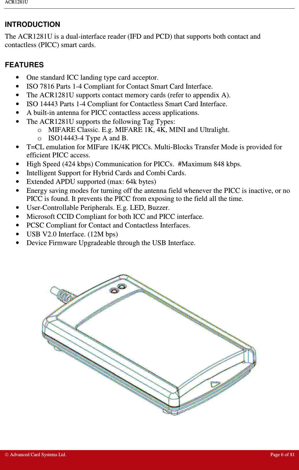
ACR1281U User Manual
Users Manual
Navigation menu
Upload a User Manual
Namespaces
Wiki Guide
HTML
PDF
Info
Views
User Manual
Discussion / Help
Navigation
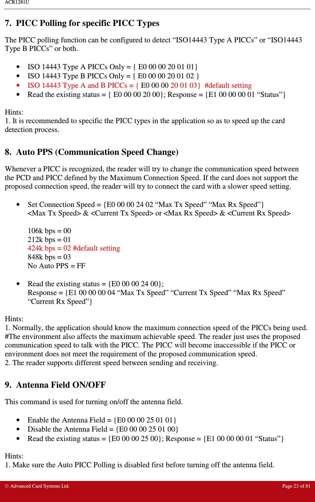
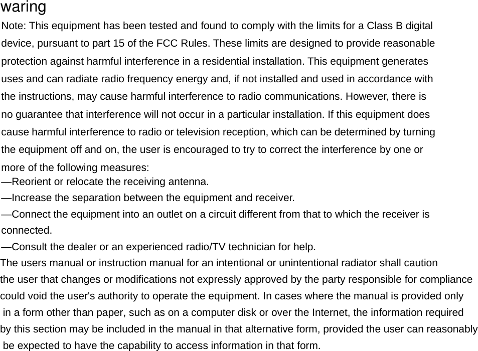
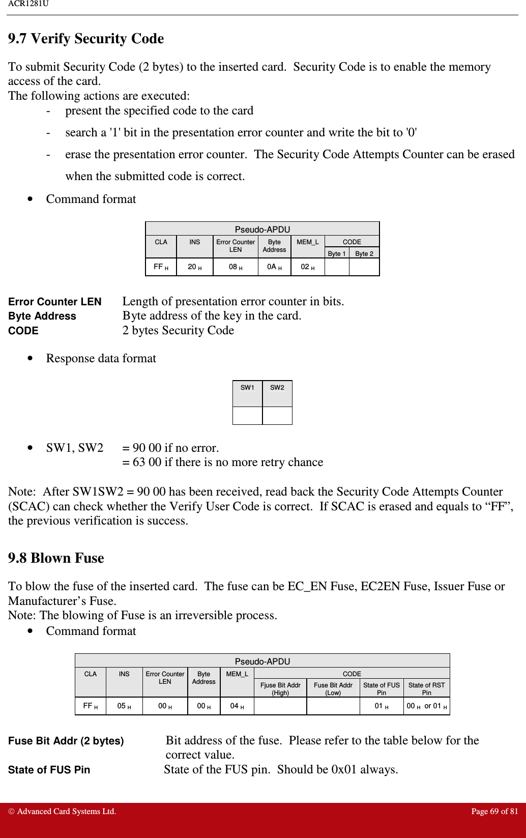
![ACR1281U Advanced Card Systems Ltd. Page 26 of 81 PICC INTERFACE DESCRIPTION 1. ATR Generation If the reader detects a PICC, an ATR will be sent to the PCSC driver for identifying the PICC. 1.1 ATR format for ISO 14443 Part 3 PICCs. Byte Value (Hex) Designation Description 0 3B Initial Header 1 8N T0 Higher nibble 8 means: no TA1, TB1, TC1 only TD1 is following. Lower nibble N is the number of historical bytes (HistByte 0 to HistByte N-1) 2 80 TD1 Higher nibble 8 means: no TA2, TB2, TC2 only TD2 is following. Lower nibble 0 means T = 0 3 01 TD2 Higher nibble 0 means no TA3, TB3, TC3, TD3 following. Lower nibble 1 means T = 1 80 T1 Category indicator byte, 80 means A status indicator may be present in an optional COMPACT-TLV data object 4F Application identifier Presence Indicator 0C Length RID Registered Application Provider Identifier (RID) # A0 00 00 03 06 SS Byte for standard C0 .. C1 Tk Bytes for card name 4 To 3+N 00 00 00 00 RFU RFU # 00 00 00 00 4+N UU TCK Exclusive-oring of all the bytes T0 to Tk e.g. ATR for MIFare 1K = {3B 8F 80 01 80 4F 0C A0 00 00 03 06 03 00 01 00 00 00 00 6A} Length (YY) = 0x0C RID = {A0 00 00 03 06} (PC/SC Workgroup) Standard (SS) = 03 (ISO14443A, Part 3) Card Name (C0 .. C1) = {00 01} (MIFare 1K) Card Name (C0 .. C1) 00 01: Mifare 1K 00 02: Mifare 4K 00 03: Mifare Ultralight 00 26: Mifare Mini FF 28: JCOP 30 FF [SAK]: undefined tags](https://usermanual.wiki/Advanced-Card-Systems/ACR1281U/User-Guide-1410644-Page-23.png)
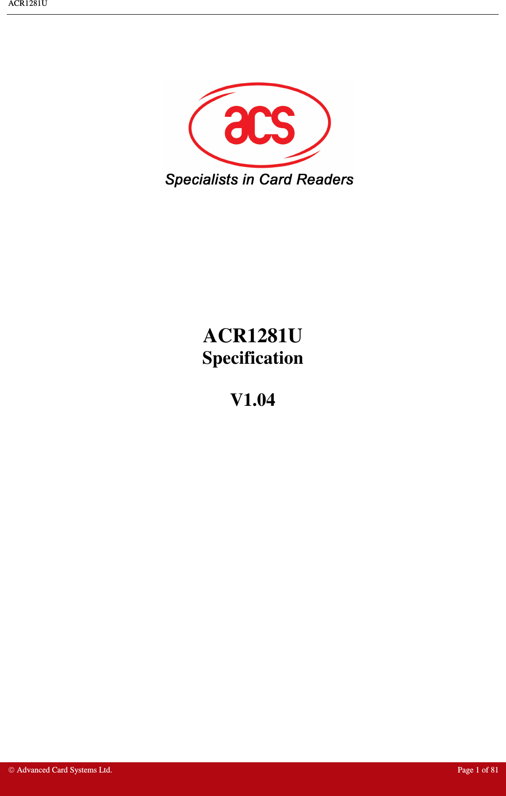
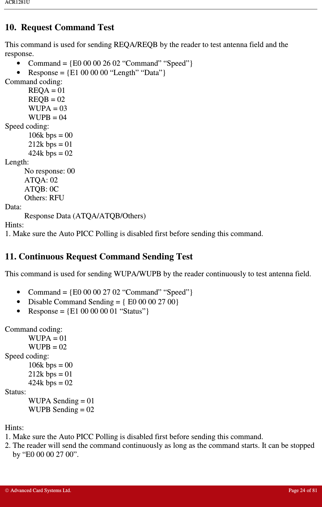
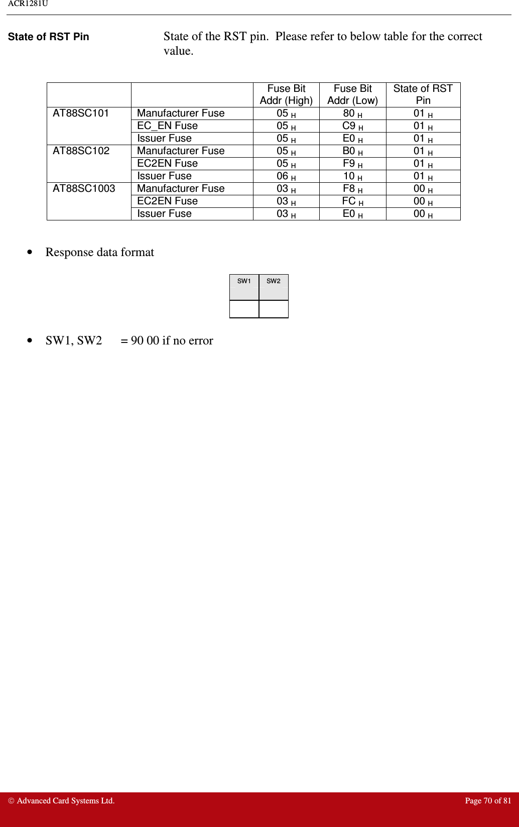
![ACR1281U Advanced Card Systems Ltd. Page 28 of 81 PICC COMMANDS FOR GENERAL PURPOSES 1. Get Data The “Get Data command” will return the serial number or ATS of the “connected PICC”. Table 1.1-1a: Get UID APDU Format (5 Bytes) Command Class INS P1 P2 Le Get Data FF CA 00 01 00 00 (Max Length) Table 2.1-1b: Get UID Response Format (UID + 2 Bytes) if P1 = 0x00 Response Data Out Result UID (LSB) UID (MSB) SW1 SW2 Table 2.1-1c: Get ATS of a ISO 14443 A card (ATS + 2 Bytes) if P1 = 0x01 Response Data Out Result ATS SW1 SW2 Table 2.1-1d: Response Codes Results SW1 SW2 Meaning Success 90 00 The operation is completed successfully. Warning 62 82 End of UID/ATS reached before Le bytes (Le is greater than UID Length). Error 6C XX Wrong length (wrong number Le: ‘XX’ encodes the exact number) if Le is less than the available UID length. Error 63 00 The operation is failed. Error 6A 81 Function not supported Examples: // To get the serial number of the “connected PICC” UINT8 GET_UID[5]={0xFF, 0xCA, 0x00, 0x00, 0x00}; // To get the ATS of the “connected ISO 14443 A PICC” UINT8 GET_ATS[5]={0xFF, 0xCA, 0x01, 0x00, 0x00};](https://usermanual.wiki/Advanced-Card-Systems/ACR1281U/User-Guide-1410644-Page-25.png)
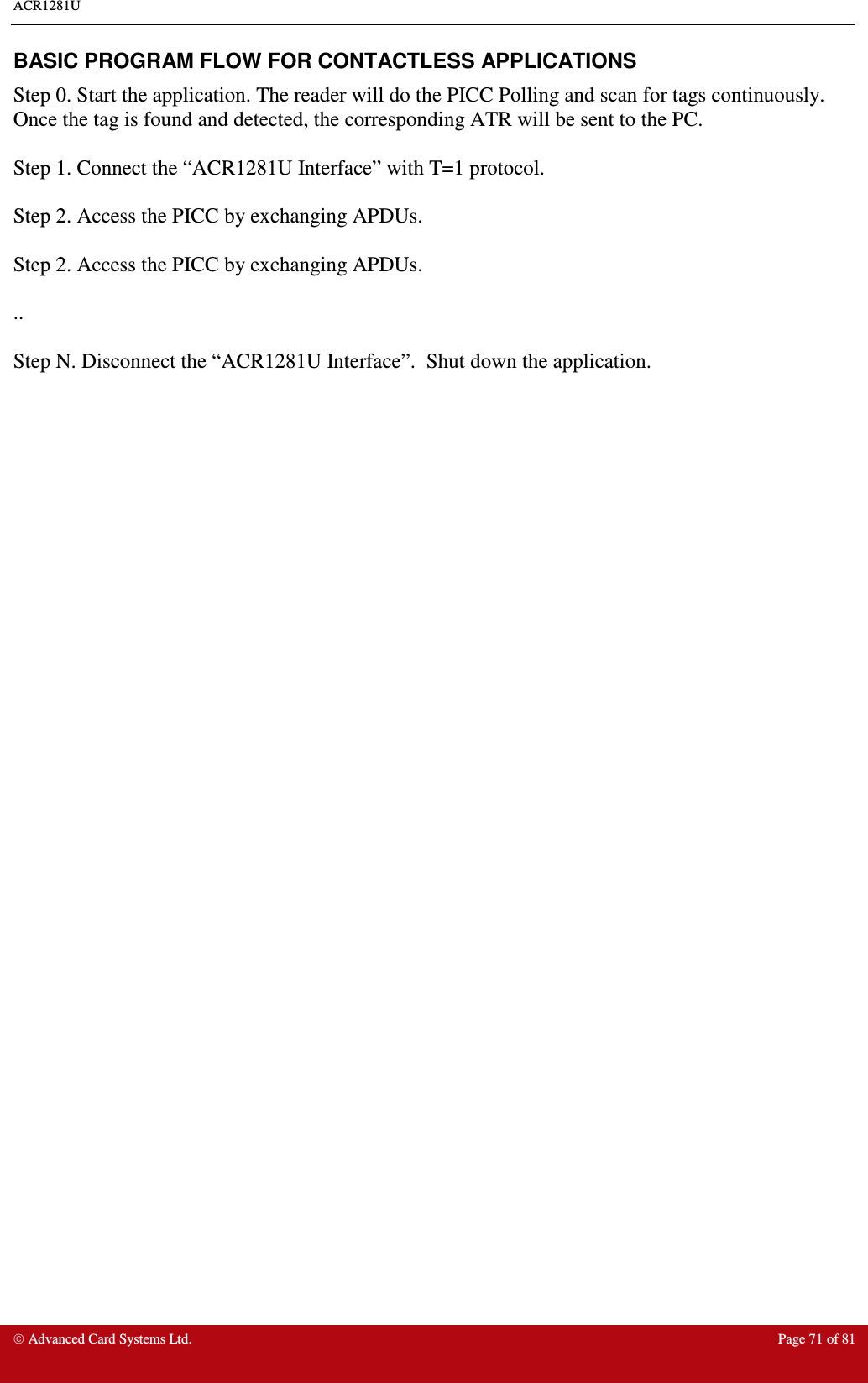
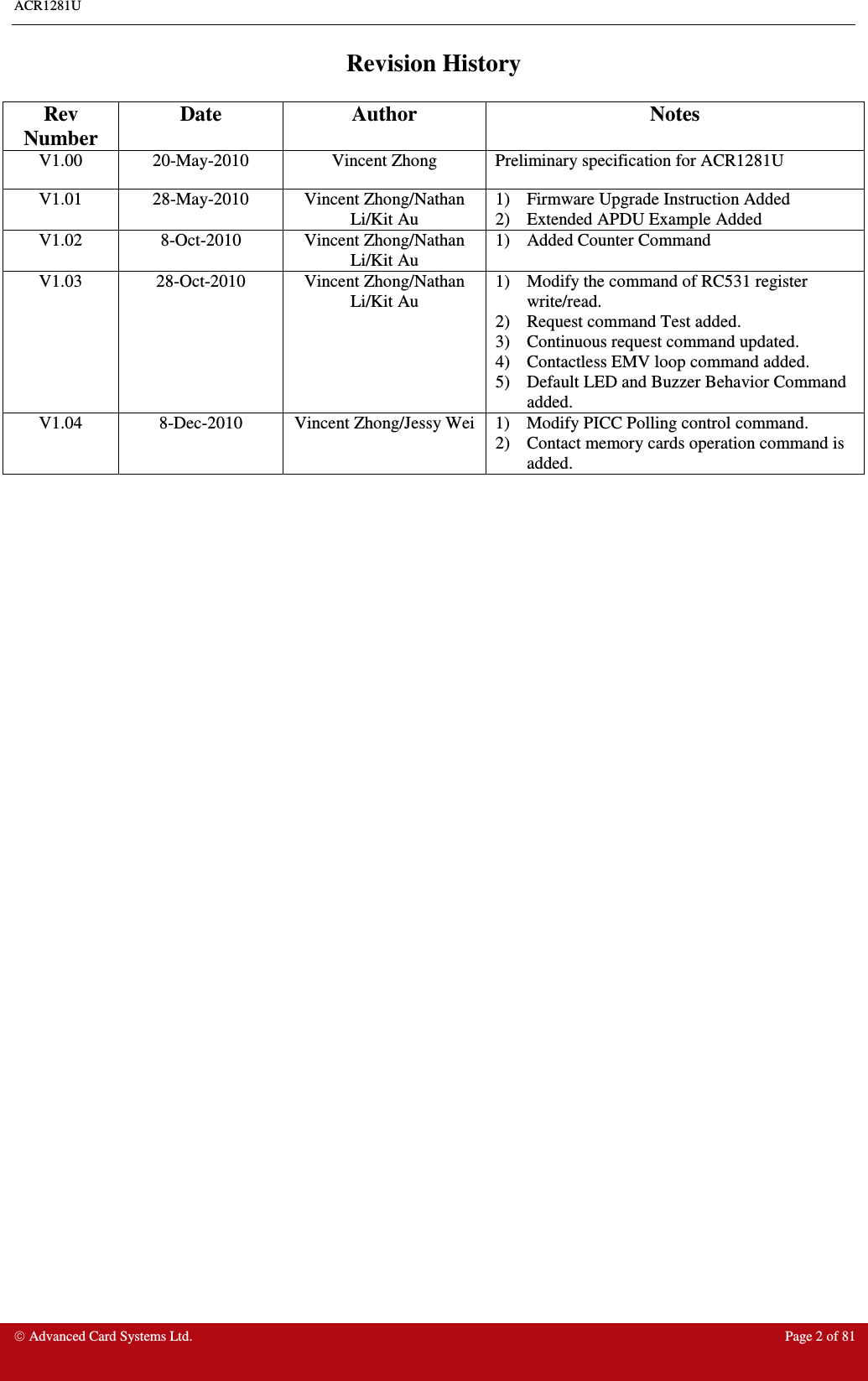
![ACR1281U Advanced Card Systems Ltd. Page 73 of 81 Typical sequence may be: - Present the Tag and Connect the PICC Interface - Read / Update the memory of the tag Step 1) Connect the Tag Step 2) Send an APDU, Get Challenge. << 00 84 00 00 08 >> D1 04 32 5A 9C E9 FF 0D [90 00] Hint: For ISO14443-4 Type A tags, the ATS can be obtained by using the APDU “FF CA 01 00 00”](https://usermanual.wiki/Advanced-Card-Systems/ACR1281U/User-Guide-1410644-Page-70.png)
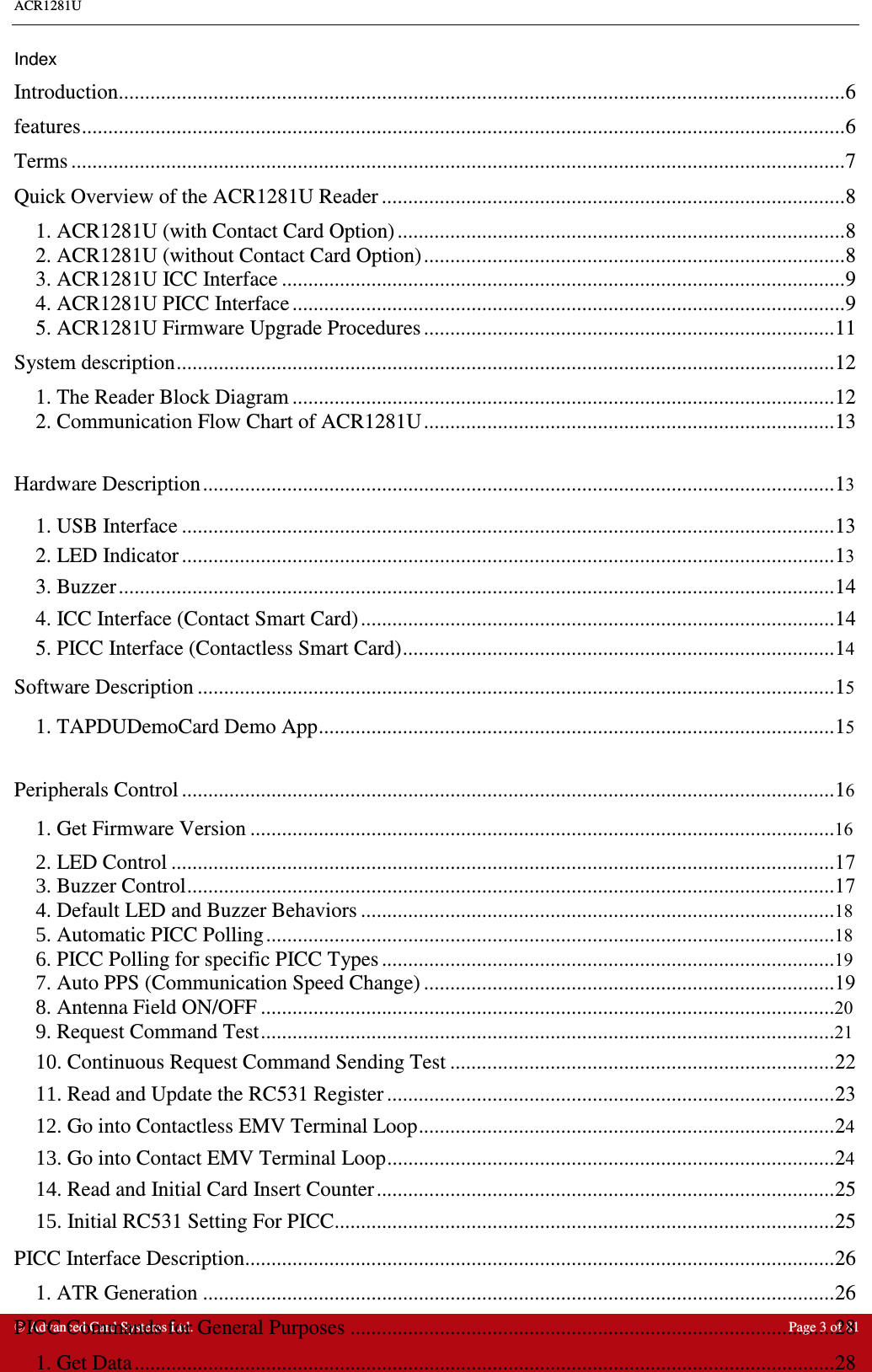
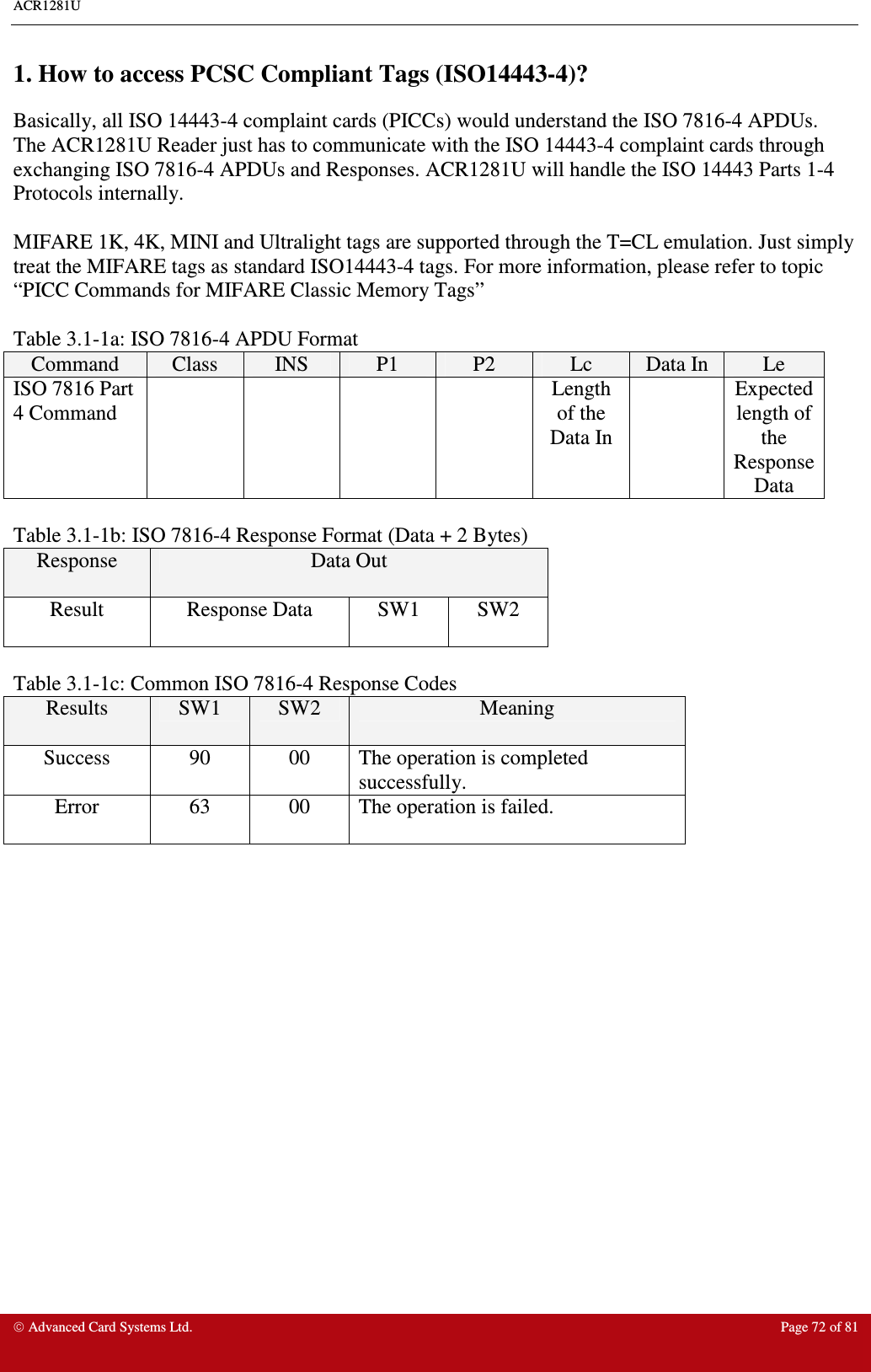
![ACR1281U Advanced Card Systems Ltd. Page 74 of 81 For Example: ISO7816-4 APDU // To read 8 bytes from an ISO 14443-4 Type B PICC (ST19XR08E) APDU ={80 B2 80 00 08} Class = 0x80 INS = 0xB2 P1 = 0x80 P2 = 0x00 Lc = None Data In = None Le = 0x08 Answer: 01 02 03 04 05 06 07 08 [$9000]](https://usermanual.wiki/Advanced-Card-Systems/ACR1281U/User-Guide-1410644-Page-71.png)
![ACR1281U Advanced Card Systems Ltd. Page 75 of 81 2. How to access DESFIRE Tags (ISO14443-4)? The DESFIRE supports ISO7816-4 APDU Wrapping and Native modes. Once the DESFire Tag is activated, the first APDU sent to the DESFire Tag will determine the “Command Mode”. If the first APDU is “Native Mode”, the rest of the APDUs must be in “Native Mode” format. Similarly, If the first APDU is “ISO7816-4 APDU Wrapping Mode”, the rest of the APDUs must be in “ISO7816-4 APDU Wrapping Mode” format. Example 1: DESFIRE ISO7816-4 APDU Wrapping. // To read 8 bytes random number from an ISO 14443-4 Type A PICC (DESFIRE) APDU = {90 0A 00 00 01 00 00} Class = 0x90; INS = 0x0A (DESFire Instruction); P1 = 0x00; P2 = 0x00 Lc = 0x01; Data In = 0x00; Le = 0x00 (Le = 0x00 for maximum length) Answer: 1A 29 06 2D 0D C4 00 A6 [$91AF] # Status Code{91 AF} is defined in DESFIRE specification. Please refer to the DESFIRE specification for more details.](https://usermanual.wiki/Advanced-Card-Systems/ACR1281U/User-Guide-1410644-Page-72.png)
![ACR1281U Advanced Card Systems Ltd. Page 76 of 81 Example 2: DESFIRE Frame Level Chaining (ISO 7816 wrapping mode) // In this example, the application has to do the “Frame Level Chaining”. // To get the version of the DESFIRE card. Step 1: Send an APDU {90 60 00 00 00} to get the first frame. INS=0x60 Answer: 04 01 01 00 02 18 05 91 AF [$91AF] Step 2: Send an APDU {90 AF 00 00 00} to get the second frame. INS=0xAF Answer: 04 01 01 00 06 18 05 91 AF [$91AF] Step 3: Send an APDU {90 AF 00 00 00} to get the last frame. INS=0xAF Answer: 04 52 5A 19 B2 1B 80 8E 36 54 4D 40 26 04 91 00 [$9100] Example 3: DESFIRE Native Command. // We can send Native DESFire Commands to the reader without ISO7816 wrapping if we find that the Native DESFire Commands are more easier to handle. // To read 8 bytes random number from an ISO 14443-4 Type A PICC (DESFIRE) APDU = {0A 00} Answer: AF DC E3 4F 26 1D 2D 51 49 [$5149] In which, the first byte “AF” is the status code returned by the DESFire Card. The Data inside the blanket [$5149]can simply be ignored by the application.](https://usermanual.wiki/Advanced-Card-Systems/ACR1281U/User-Guide-1410644-Page-73.png)
![ACR1281U Advanced Card Systems Ltd. Page 77 of 81 Example 4: DESFIRE Frame Level Chaining (Native Mode) // In this example, the application has to do the “Frame Level Chaining”. // To get the version of the DESFIRE card. Step 1: Send an APDU {60} to get the first frame. INS=0x60 Answer: AF 04 01 01 00 02 18 05[$1805] Step 2: Send an APDU {AF} to get the second frame. INS=0xAF Answer: AF 04 01 01 00 06 18 05[$1805] Step 3: Send an APDU {AF} to get the last frame. INS=0xAF Answer: 00 04 52 5A 19 B2 1B 80 8E 36 54 4D 40 26 04[$2604] Hints: In DESFIRE Native Mode, the status code [90 00] will not be added to the response if the response length is greater than 1. If the response length is less than 2, the status code [90 00] will be added in order to meet the requirement of PCSC. The minimum response length is 2.](https://usermanual.wiki/Advanced-Card-Systems/ACR1281U/User-Guide-1410644-Page-74.png)