Advanced Card Systems ACR122L Contactless Smart Card Reader and Writer User Manual
Advanced Card Systems Limited Contactless Smart Card Reader and Writer Users Manual
UserManual.wiki
>
Advanced Card Systems
>
ACR122L User Manual
Users Manual
Navigation menu
Upload a User Manual
Namespaces
Wiki Guide
HTML
PDF
Info
Views
User Manual
Discussion / Help
Navigation

![ACR122L-ACS Design Specification Version 0.03 19/05/2010 Page 10 of 50 ACR122L-ACSRDR = ACR122L; HOST = Host Controller. HOST_to_RDR = Host Controller -> ACR122L RDR_to_HOST = ACR122L -> Host Controller Protocol Flow Examples(Use SAM Interface 1 as Example) 1) Activate a SAM HOST RDR 1. HOST sends a frame 02 62 00 00 00 00 00 01 01 00 00 [Checksum] 03 2. RDR sends back a positive status frame immediately 02 00 00 03 (positive status frame) .. After some processing delay... 3. RDR sends back the response of the command 02 80 0D 00 00 00 00 01 00 00 00 3B 2A 00 80 65 24 B0 00 02 00 82 90 00 [Checksum] 03 2) Activate a SAM (Incorrect Checksum, HOST) HOST RDR 1. HOST sends a corrupted frame 02 62 00 00 00 00 00 01 01 00 00 [Incorrect Checksum] 03 2. RDR sends back a negative status frame immediately 02 FF FF 03 (negative status frame) 3. HOST sends the frame again. 02 62 00 00 00 00 00 01 01 00 00 [Checksum] 03 4. RDR sends back a positive status frame immediately 02 00 00 03 (positive status frame) .. After some processing delay... 5. RDR sends back the response of the command 02 80 0D 00 00 00 00 01 00 00 00 3B 2A 00 80 65 24 B0 00 02 00 82 90 00 [Checksum] 03 ](https://usermanual.wiki/Advanced-Card-Systems/ACR122L/User-Guide-1354295-Page-10.png)
![ACR122L-ACS Design Specification Version 0.03 19/05/2010 Page 11 of 50 ACR122L-ACS 3) Activate a SAM (Incorrect Checksum, RDR) HOST RDR 1. HOST sends a frame 02 62 00 00 00 00 00 01 01 00 00 [Checksum] 03 2. RDR sends back a positive status frame immediately 02 00 00 03 (positive status frame) .. After some processing delay... 3. RDR sends back the response (corrupted) of the command 4. HOST sends a NAK frame to get the response again. 5. RDR sends back the response of the command 02 80 0D 00 00 00 00 01 00 00 00 3B 2A 00 80 65 24 B0 00 02 00 82 90 00 [Incorrect Checksum] 03 02 00 00 00 00 00 00 00 00 00 00 00 03 (NAK) 02 80 0D 00 00 00 00 01 00 00 00 3B 2A 00 80 65 24 B0 00 02 00 82 90 00 [Checksum] 03 Remarks: If the frame sent by the HOST is correctly received by the RDR, a positive status frame = {02 00 00 03} will be sent to the HOST immediately to inform the HOST the frame is correctly received. The HOST has to wait for the response of the command. The RDR will not receive any more frames while the command is being processed. In case of errors, a negative status frame will be sent to the HOST to indicate the frame is either corrupted or wrong formatted. - CheckSum Error Frame = {02 FF FF 03} - Length Error Frame = {02 FE FE 03}. The length “dDwLength” is greater than 0x0105 bytes. - ETX Error Frame = {02 FD FD 03}. The last byte is not equal to ETX “0x03”. - TimeOut Error Frame = {02 FC FC 03}. Not Complete Package Received. The NAK Frame is only used by the HOST to get the last response. {02 00 00 00 00 00 00 00 00 00 00 00 03} // 11 zeros](https://usermanual.wiki/Advanced-Card-Systems/ACR122L/User-Guide-1354295-Page-11.png)
![ACR122L-ACS Design Specification Version 0.03 19/05/2010 Page 13 of 50 ACR122L-ACSRDR_to_HOST_DataBlock Format Offset Field Size Value Description 0 bMessageType 1 80h Indicates that a data block is being sent from the ACR122L 1 dwLength <LSB .. MSB> 4 N Size of abData field. (N Bytes) 5 bSlot 1 Same as Bulk-OUT Identifies the slot number for this command 6 bSeq 1 Same as Bulk-OUT Sequence number for corresponding command 7 bStatus 1 8 bError 1 9 bChainParameter 1 Example1. To activate the SAM Interface 1 slot 0 (default), sequence number = 1, 5V card. HOST -> 02 62 00 00 00 00 00 01 01 00 00 [Checksum] 03 RDR -> 02 00 00 03 RDR -> 02 80 0D 00 00 00 00 01 00 00 00 3B 2A 00 80 65 24 B0 00 02 00 82 90 00 [Checksum] 03 The ATR = 3B 2A 00 80 65 24 B0 00 02 00 82; SW1 SW2 = 90 00 Example2. To activate the SAM Interface 2 slot 0 (default), sequence number = 1, 5V card. HOST -> 12 62 00 00 00 00 00 01 01 00 00 [Checksum] 13 RDR -> 12 00 00 13 RDR -> 12 80 0D 00 00 00 00 01 00 00 00 3B 2A 00 80 65 24 B0 00 02 00 82 90 00 [Checksum] 13 The ATR = 3B 2A 00 80 65 24 B0 00 02 00 82; SW1 SW2 = 90 00 Example3. To activate the SAM Interface 3 slot 0 (default), sequence number = 1, 5V card. HOST -> 22 62 00 00 00 00 00 01 01 00 00 [Checksum] 23 RDR -> 22 00 00 23 RDR -> 22 80 0D 00 00 00 00 01 00 00 00 3B 2A 00 80 65 24 B0 00 02 00 82 90 00 [Checksum] 23 The ATR = 3B 2A 00 80 65 24 B0 00 02 00 82; SW1 SW2 = 90 00](https://usermanual.wiki/Advanced-Card-Systems/ACR122L/User-Guide-1354295-Page-13.png)
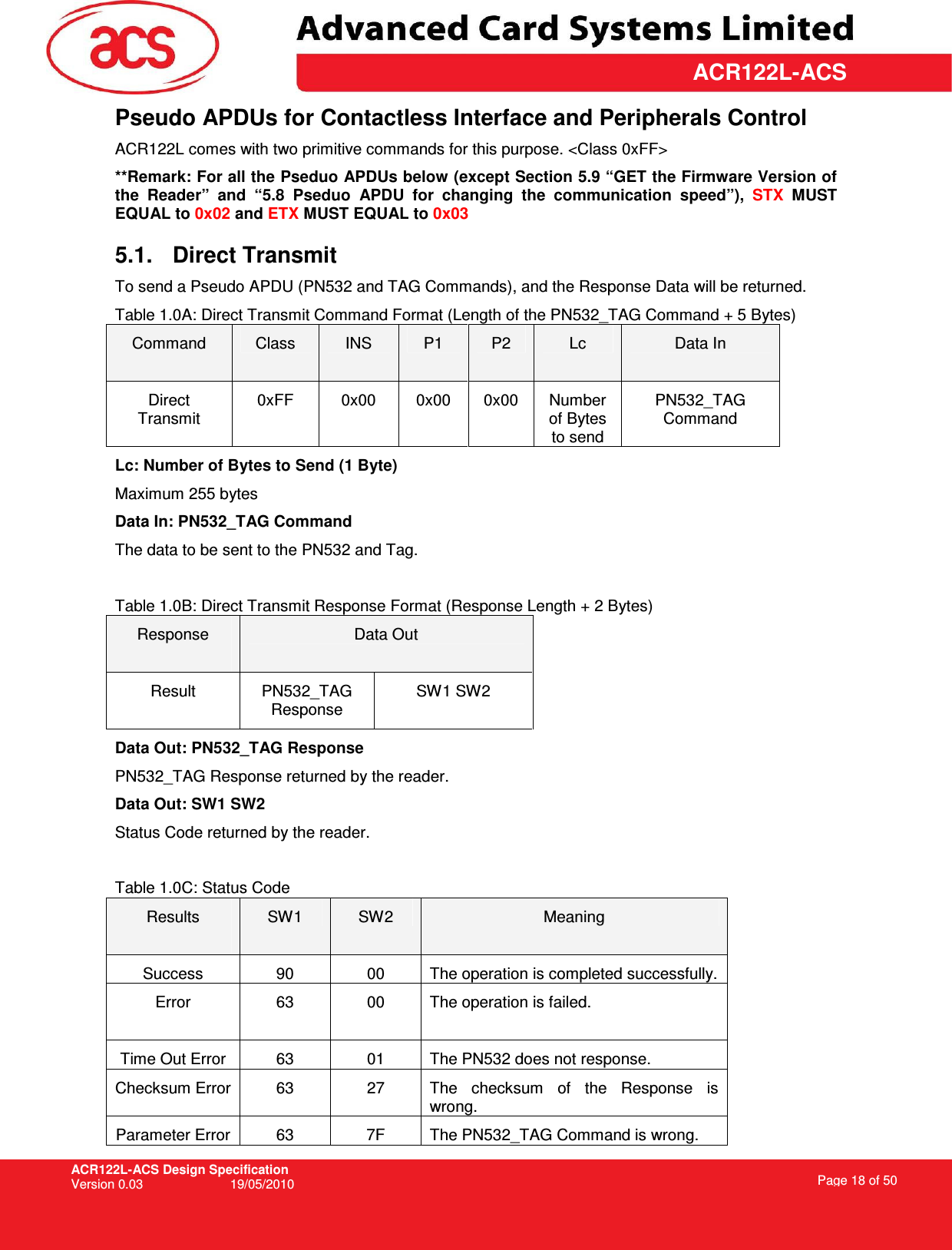
![ACR122L-ACS Design Specification Version 0.03 19/05/2010 Page 15 of 50 ACR122L-ACSExample1. To deactivate the SAM Interface 1 slot 0 (default), sequence number = 2. HOST -> 02 63 00 00 00 00 00 02 00 00 00 [Checksum] 03 RDR -> 02 00 00 03 RDR -> 02 81 00 00 00 00 00 02 00 00 00 [Checksum] 03 Example2. To deactivate the SAM Interface 2 slot 0 (default), sequence number = 2. HOST -> 12 63 00 00 00 00 00 02 00 00 00 [Checksum] 13 RDR -> 12 00 00 13 RDR -> 12 81 00 00 00 00 00 02 00 00 00 [Checksum] 13 Example3. To deactivate the SAM Interface 3 slot 0 (default), sequence number = 2. HOST -> 22 63 00 00 00 00 00 02 00 00 00 [Checksum] 23 RDR -> 22 00 00 23 RDR -> 22 81 00 00 00 00 00 02 00 00 00 [Checksum] 23 To do data-exchange through the SAM Interface ACR122L Command Frame Format STX Bulk-OUT Header (HOST_to_RDR_XfrBlock) Parameters Checksum ETX 1 Byte 10 Bytes M Byte 1 Byte 1 Byte For SAM Interface 1, STX = 0x02 and ETX = 0x03 For SAM Interface 2, STX = 0x12 and ETX = 0x13 For SAM Interface 3, STX = 0x22 and ETX = 0x23 HOST_to_RDR_XfrBlock Format Offset Field Size Value Description 0 bMessageType 1 6Fh 1 dDwLength <LSB .. MSB> 4 M Message-specific data length 5 bSlot 1 00-FFh Identifies the slot number for this command. Default=00h 6 bSeq 1 00-FFh Sequence number for command 7 bBWI 1 00-FFh Used to extend the Block Waiting Timeout. 8 wLevelParameter 2 0000h](https://usermanual.wiki/Advanced-Card-Systems/ACR122L/User-Guide-1354295-Page-15.png)
![ACR122L-ACS Design Specification Version 0.03 19/05/2010 Page 16 of 50 ACR122L-ACS ACR122L Response Frame Format STX Bulk-IN Header (RDR_to_HOST_DataBlock) abData Checksum ETX 1 Byte 10 Bytes N Bytes (ATR) 1 Byte 1 Byte For SAM Interface 1, STX = 0x02 and ETX = 0x03 For SAM Interface 2, STX = 0x12 and ETX = 0x13 For SAM Interface 3, STX = 0x22 and ETX = 0x23 RDR_to_HOST_DataBlock Format Offset Field Size Value Description 0 bMessageType 1 80h Indicates that a data block is being sent from the ACR122L 1 dwLength <LSB .. MSB> 4 N Size of abData field. (N Bytes) 5 bSlot 1 Same as Bulk-OUT Identifies the slot number for this command 6 bSeq 1 Same as Bulk-OUT Sequence number for corresponding command 7 bStatus 1 8 bError 1 9 bChainParameter 1 Example1. To send an APDU “80 84 00 00 08” to the SAM Interface 1 slot 0 (default), sequence number = 3. HOST -> 02 6F 05 00 00 00 00 03 00 00 00 80 84 00 00 08 [Checksum] 03 RDR -> 02 00 00 03 RDR -> 02 80 0A 00 00 00 00 03 00 00 00 E3 51 B0 FC 88 AA 2D 18 90 00 [Checksum] 03 Response = E3 51 B0 FC 88 AA 2D 18; SW1 SW2 = 90 00 Example2. To send an APDU “80 84 00 00 08” to the SAM Interface 2 slot 0 (default), sequence number = 3. HOST -> 12 6F 05 00 00 00 00 03 00 00 00 80 84 00 00 08 [Checksum] 13 RDR -> 12 00 00 13 RDR -> 12 80 0A 00 00 00 00 03 00 00 00 E3 51 B0 FC 88 AA 2D 18 90 00 [Checksum] 13 Response = E3 51 B0 FC 88 AA 2D 18; SW1 SW2 = 90 00](https://usermanual.wiki/Advanced-Card-Systems/ACR122L/User-Guide-1354295-Page-16.png)
![ACR122L-ACS Design Specification Version 0.03 19/05/2010 Page 17 of 50 ACR122L-ACSExample3. To send an APDU “80 84 00 00 08” to the SAM Interface 3 slot 0 (default), sequence number = 3. HOST -> 22 6F 05 00 00 00 00 03 00 00 00 80 84 00 00 08 [Checksum] 23 RDR -> 22 00 00 23 RDR -> 22 80 0A 00 00 00 00 03 00 00 00 E3 51 B0 FC 88 AA 2D 18 90 00 [Checksum] 23 Response = E3 51 B0 FC 88 AA 2D 18; SW1 SW2 = 90 00](https://usermanual.wiki/Advanced-Card-Systems/ACR122L/User-Guide-1354295-Page-17.png)
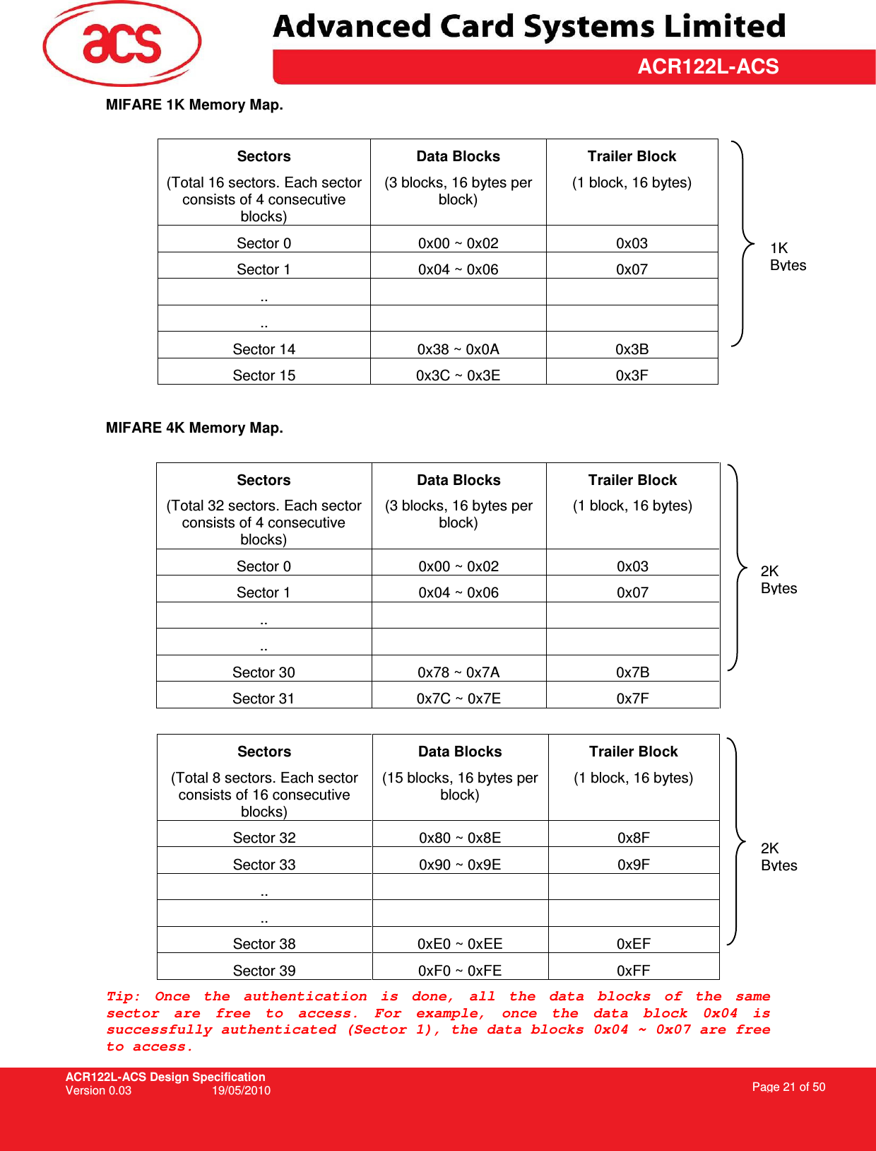
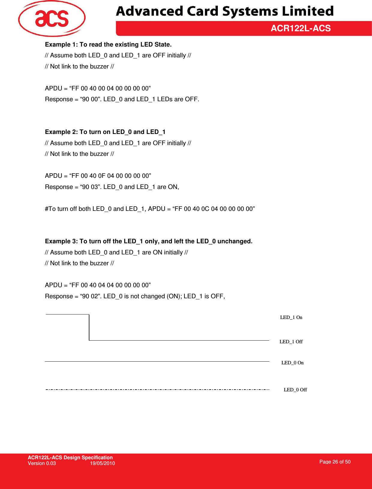
![ACR122L-ACS Design Specification Version 0.03 19/05/2010 Page 19 of 50 ACR122L-ACS Example 1. How to access MIFARE Classic Tags? Typical sequence may be: - Scanning the tags in the field (Polling) - Authentication - Read / Write the memory of the tag - Halt the tag (optional) Step 1) Polling for the MIFARE 1K/4K Tags, 106 kbps << 02 6F 09 00 00 00 00 01 00 00 00 FF 00 00 00 04 D4 4A 01 00 [Checksum] 03 >> 02 00 00 03 >> 02 80 0E 00 00 00 00 01 01 00 00 D5 4B 01 01 00 02 18 04 F6 8E 2A 99 90 00 [Checksum] 03 In which, Number of Tag found = [01]; Target number = 01 SENS_RES = 00 02; SEL_RES = 18, Length of the UID = 4; UID = F6 8E 2A 99 Operation Finished = 90 00 Tip: The tag type can be determined by recognizing the SEL_RES. SEL_RES of some common tag types. 00 = MIFARE Ultralight 08 = MIFARE 1K 09 = MIFARE MINI 18 = MIFARE 4K 20 = MIFARE DESFIRE 28 = JCOP30 98 = Gemplus MPCOS Step 2) KEY A Authentication, Block 04, KEY = FF FF FF FF FF FF, UID = F6 8E 2A 99 << 02 6F 14 00 00 00 00 00 01 00 00 00 FF 00 00 00 0F D4 40 01 60 04 FF FF FF FF FF FF F6 8E 2A 99 [Checksum] 03 >> 02 00 00 03 >> 02 80 05 00 00 00 00 01 01 00 00 D5 41 [00] 90 00 [Checksum] 03](https://usermanual.wiki/Advanced-Card-Systems/ACR122L/User-Guide-1354295-Page-19.png)
![ACR122L-ACS Design Specification Version 0.03 19/05/2010 Page 20 of 50 ACR122L-ACS Tip: If the authentication failed, the error code [XX] will be returned. [00] = Valid, other = Error. Please refer to Error Codes Table for more details. Tip: For KEY B Authentication << 02 6F 14 00 00 00 00 00 01 00 00 00 FF 00 00 00 0F D4 40 01 61 04 FF FF FF FF FF FF F6 8E 2A 99 [Checksum] 03 Step 3) Read the content of Block 04 << 02 6F 0A 00 00 00 00 01 00 00 00 FF 00 00 00 05 D4 40 01 30 04 [Checksum] 03 >> 02 00 00 03 >> 02 80 05 00 00 00 00 01 01 00 00 D5 41 [00] 01 02 03 04 05 06 07 08 09 10 11 12 13 14 15 16 90 00 [Checksum] 03 In which, Block Data = 01 02 03 04 05 06 07 08 09 10 11 12 13 14 15 16 Step 4) Update the content of Block 04 << 02 6F 1A 00 00 00 00 01 00 00 00 FF 00 00 00 15 D4 40 01 A0 04 01 02 03 04 05 06 07 08 09 0A 0B 0C 0D 0E 0F 10 [Checksum] 03 >> 02 00 00 03 >> 02 6F 0A 00 00 00 00 01 00 00 00 FF 00 00 00 05 D5 41 [00] 90 00 [Checksum] 03 Step 5) Halt the tag (optional) << 02 6F 08 00 00 00 00 01 00 00 00 FF 00 00 00 03 D4 44 01 [Checksum] 03 >> 02 00 00 03 >> 02 80 05 00 00 00 00 01 01 00 00 D5 45 [00] 90 00 [Checksum] 03](https://usermanual.wiki/Advanced-Card-Systems/ACR122L/User-Guide-1354295-Page-20.png)
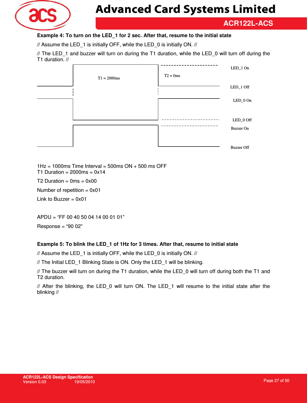
![ACR122L-ACS Design Specification Version 0.03 19/05/2010 Page 22 of 50 ACR122L-ACS Example 2. How to handle Value Blocks of MIFARE 1K/4K Tag? The value blocks are used for performing electronic purse functions. E.g. Increment, Decrement, Restore and Transfer .. etc. The value blocks have a fixed data format which permits error detection and correction and a backup management. Byte Number 0 1 2 3 4 5 6 7 8 9 10 11 12 13 14 15 Description Value ______ Value Value Adr ___ Adr Adr ___ Adr Value: A signed 4-Byte value. The lowest significant byte off a value is stored in the lowest address byte. Negative values are stored in standard 2’s complement format. Adr: 1-Byte address, which can be used to save the storage address of a block. (optional) e.g. Value 100 (decimal) = 64 (Hex), assume Block = 0x05 The formatted value block = 64 00 00 00 9B FF FF FF 64 00 00 00 05 FA 05 FA Step 1) Update the content of Block 05 with a value 100 (dec) << 02 6F 1A 00 00 00 00 01 00 00 00 FF 00 00 00 15 D4 40 01 A0 05 64 00 00 00 9B FF FF FF 64 00 00 00 05 FA 05 FA [Checksum] 03 >> 02 6F 0A 00 00 00 00 01 00 00 00 FF 00 00 00 05 D5 41 [00] 90 00 [Checksum] 03 Step 2) Increment the value of Block 05 by 1 (dec) << 02 6F 0E 00 00 00 00 01 00 00 00 FF 00 00 00 09 D4 40 01 C1 05 01 00 00 00 [Checksum] 03 >> 02 6F 0A 00 00 00 00 01 00 00 00 FF 00 00 00 05 D5 41 [00] 90 00 [Checksum] 03 Tip: Decrement the value of Block 05 by 1 (dec) << 02 6F 0E 00 00 00 00 01 00 00 00 FF 00 00 00 09 D4 40 01 C0 05 01 00 00 00 [Checksum] 03 Step 3) Transfer the prior calculated value of Block 05 (dec) << 02 6F 0A 00 00 00 00 01 00 00 00 FF 00 00 00 05 D4 40 01 B0 05 [Checksum] 03](https://usermanual.wiki/Advanced-Card-Systems/ACR122L/User-Guide-1354295-Page-22.png)
![ACR122L-ACS Design Specification Version 0.03 19/05/2010 Page 23 of 50 ACR122L-ACS>> 02 6F 0A 00 00 00 00 01 00 00 00 FF 00 00 00 05 D5 41 [00] 90 00 [Checksum] 03 Tip: Restore the value of Block 05 (cancel the prior Increment or Decrement operation) << 02 6F 0A 00 00 00 00 01 00 00 00 FF 00 00 00 05 D4 40 01 C2 05 [Checksum] 03 Step 4) Read the content of Block 05 << 02 6F 0A 00 00 00 00 01 00 00 00 FF 00 00 00 05 D4 40 01 30 05 [Checksum] 03 >> 02 6F 1A 00 00 00 00 01 00 00 00 FF 00 00 00 05 D5 41 [00] 65 00 00 00 9A FF FF FF 65 00 00 00 05 FA 05 FA 90 00 [Checksum] 03 In which, the value = 101 (dec) Step 5) Copy the value of Block 05 to Block 06 (dec) << 02 6F 0A 00 00 00 00 01 00 00 00 FF 00 00 00 05 D4 40 01 C2 05 [Checksum] 03 >> 02 6F 0A 00 00 00 00 01 00 00 00 FF 00 00 00 05 D5 41 [00] 90 00 [Checksum] 03 << 02 6F 0A 00 00 00 00 01 00 00 00 FF 00 00 00 05 D4 40 01 B0 06 [Checksum] 03 >> 02 6F 0A 00 00 00 00 01 00 00 00 FF 00 00 00 05 D5 41 [00] 90 00 [Checksum] 03 Step 6) Read the content of Block 06 << 02 6F 0A 00 00 00 00 01 00 00 00 FF 00 00 00 05 D4 40 01 30 06 [Checksum] 03 >> 02 6F 1A 00 00 00 00 01 00 00 00 FF 00 00 00 15 D5 41 [00] 65 00 00 00 9A FF FF FF 65 00 00 00 05 FA 05 FA 90 00 [Checksum] 03 In which, the value = 101 (dec). The Adr “05 FA 05 FA” tells us the value is copied from Block 05.](https://usermanual.wiki/Advanced-Card-Systems/ACR122L/User-Guide-1354295-Page-23.png)
![ACR122L-ACS Design Specification Version 0.03 19/05/2010 Page 42 of 50 ACR122L-ACSExample 1: To initialize a FeliCa Tag (Tag Polling) Step 1: Issue a “Direct Transmit” APDU. The APDU Command should be “FF 00 00 00 09 D4 4A 01 01 00 FF FF 01 00” #In which, Direct Transmit APDU = “FF 00 00 00” Length of the PN532_Tag Command = “09” PN532 Command (InListPassiveTarget 212Kbps) = “D4 4A 01 01” Tag Command (System Code Request) = “00 FF FF 01 00” To send an APDU to the slot 0 (default), sequence number = 1. HOST -> 02 6F 0E 00 00 00 00 01 00 00 00 FF 00 00 00 09 D4 4A 01 01 00 FF FF 01 00 [Checksum] 03 RDR -> 02 00 00 03 RDR -> 02 81 1A 00 00 00 00 01 00 00 00 D5 4B 01 01 14 01 01 01 05 01 86 04 02 02 03 00 4B 02 4F 49 8A 8A 80 08 90 00 [Checksum] 03 The APDU Response is “D5 4B 01 01 14 01 01 01 05 01 86 04 02 02 03 00 4B 02 4F 49 8A 8A 80 08 90 00” #In which, Response returned by the PN532 = “D5 4B 01 01 14 01 01 01 05 01 86 04 02 02 03 00 4B 02 4F 49 8A 8A 80 08” NFCID2t of the FeliCa Tag = “01 01 05 01 86 04 02 02” Status Code returned by the reader = “90 00”](https://usermanual.wiki/Advanced-Card-Systems/ACR122L/User-Guide-1354295-Page-42.png)
![ACR122L-ACS Design Specification Version 0.03 19/05/2010 Page 43 of 50 ACR122L-ACSExample 2: To write 16 bytes data to the FeliCa Tag (Tag Write) Step 1: Issue a “Direct Transmit” APDU. The APDU Command should be “FF 00 00 00 23 D4 40 01 20 08 01 01 05 01 86 04 02 02 01 09 01 01 80 00 00 AA 55 AA 55 AA 55 AA 55 AA 55 AA 55 AA 55 AA” #In which, Direct Transmit APDU = “FF 00 00 00” Length of the PN532_Tag Command = “23” PN532 Command (InDataExchange) = “D4 40 01” Tag Command (Write Data) = “20 08 01 01 05 01 86 04 02 02 01 09 01 01 80 00 00 AA 55 AA 55 AA 55 AA 55 AA 55 AA 55 AA 55 AA”. To send an APDU to the slot 0 (default), sequence number = 2. HOST -> 02 6F 28 00 00 00 00 02 00 00 00 FF 00 00 00 00 23 D4 40 01 20 08 01 01 05 01 86 04 02 02 01 09 01 01 80 00 00 AA 55 AA 55 AA 55 AA 55 AA 55 AA 55 AA [Checksum] 03 RDR -> 02 00 00 03 RDR -> 02 81 11 00 00 00 00 02 00 00 00 D5 41 00 0C 09 01 01 05 01 86 04 02 02 00 00 90 00 [Checksum] 03 The APDU Response would be “D5 41 00 0C 09 01 01 05 01 86 04 02 02 00 00 90 00” #In which, Response returned by the PN532 = “D5 41” Response returned by the FeliCa Tag = “00 0C 09 01 01 05 01 86 04 02 02 00 00” Status Code returned by the reader = “90 00”](https://usermanual.wiki/Advanced-Card-Systems/ACR122L/User-Guide-1354295-Page-43.png)
![ACR122L-ACS Design Specification Version 0.03 19/05/2010 Page 44 of 50 ACR122L-ACSExample 3: To read 16 bytes data from the FeliCa Tag (Tag Write) Step 1: Issue a “Direct Transmit” APDU. The APDU Command should be “FF 00 00 00 13 D4 40 01 10 06 01 01 05 01 86 04 02 02 01 09 01 01 80 00” #In which, Direct Transmit APDU = “FF 00 00 00” Length of the PN532_Tag Command = “13” PN532 Command (InDataExchange) = “D4 40 01” Tag Command (Read Data) = “10 06 01 01 05 01 86 04 02 02 01 09 01 01 80 00” To send an APDU to the slot 0 (default), sequence number = 3. HOST -> 02 6F 18 00 00 00 00 03 00 00 00 FF 00 00 00 13 D4 40 01 10 06 01 01 05 01 86 04 02 02 01 09 01 01 80 00 FF [Checksum] 03 RDR -> 02 00 00 03 RDR -> 02 81 22 00 00 00 00 03 00 00 00 D5 41 00 1D 07 01 01 05 01 86 04 02 02 00 00 01 00 AA 55 AA 55 AA 55 AA 55 AA 55 AA 55 AA 55 AA 90 00 [Checksum] 03 The APDU Response would be “D5 41 00 1D 07 01 01 05 01 86 04 02 02 00 00 01 00 AA 55 AA 55 AA 55 AA 55 AA 55 AA 55 AA 55 AA 90 00” #In which, Response returned by the PN532 = “D5 41” Response returned by the FeliCa Tag = “00 1D 07 01 01 05 01 86 04 02 02 00 00 01 00 AA 55 AA 55 AA 55 AA 55 AA 55 AA 55 AA 55 AA” Status Code returned by the reader = “90 00”](https://usermanual.wiki/Advanced-Card-Systems/ACR122L/User-Guide-1354295-Page-44.png)
![ACR122L-ACS Design Specification Version 0.03 19/05/2010 Page 45 of 50 ACR122L-ACSExample 4: To initialize an ISO 14443-4 Type B Tag (Tag Polling) Step 1: Issue a “Direct Transmit” APDU. The APDU Command should be “FF 00 00 00 05 D4 4A 01 03 00” #In which, Direct Transmit APDU = “FF 00 00 00” Length of the PN532_Tag Command = “05” PN532 Command (InListPassiveTarget Type B 106Kbps) = “D4 4A 01 03 00” To send an APDU to the slot 0 (default), sequence number = 4. HOST -> 02 6F 0A 00 00 00 00 04 00 00 00 FF 00 00 00 05 D4 4A 01 03 00 [Checksum] 03 RDR -> 02 00 00 03 RDR -> 02 81 14 00 00 00 00 04 00 00 00 D5 41 01 01 50 00 01 32 F4 00 00 00 00 33 81 81 01 21 90 00 [Checksum] 03 The APDU Response is “D5 4B 01 01 50 00 01 32 F4 00 00 00 00 33 81 81 01 21 90 00” #In which, Response returned by the PN532 = “D5 4B 01 01” ATQB of the Type B Tag = “50 00 01 32 F4 00 00 00 00 33 81 81” CRC-B = “01 21” Status Code returned by the reader = “90 00”](https://usermanual.wiki/Advanced-Card-Systems/ACR122L/User-Guide-1354295-Page-45.png)
![ACR122L-ACS Design Specification Version 0.03 19/05/2010 Page 46 of 50 ACR122L-ACSExample 5: To send an APDU to an ISO 14443-4 Type B Tag (Data Exchange) Step 1: Issue a “Direct Transmit” APDU. The USER APDU Command should be “00 84 00 00 08” The Composed APDU Command should be “FF 00 00 00 08 D4 40 01 00 84 00 00 08” #In which, Direct Transmit APDU = “FF 00 00 00” Length of the PN532_Tag Command = “08” PN532 Command (InDataExchange) = “D4 40 01” Tag Command (Get Challenge) = “00 84 00 00 08” To send an APDU to the slot 0 (default), sequence number = 5. HOST -> 02 6F 0D 00 00 00 00 05 00 00 00 FF 00 00 00 08 D4 40 01 00 84 00 00 08 [Checksum] 03 RDR -> 02 00 00 03 RDR -> 02 81 0F 00 00 00 00 05 00 00 00 D5 41 00 01 02 03 04 05 06 07 08 90 00 90 00 [Checksum] 03 The APDU Response is “D5 41 00 0B 01 02 03 04 05 06 07 08 90 00” #In which, Response returned by the PN532 = “D5 41 00” Response from the Type B Tag = “01 02 03 04 05 06 07 08 90 00” Status Code returned by the reader = “90 00”](https://usermanual.wiki/Advanced-Card-Systems/ACR122L/User-Guide-1354295-Page-46.png)